EP1811650A1 - Method for finely tuning the frequency of a radio signal - Google Patents
Method for finely tuning the frequency of a radio signal Download PDFInfo
- Publication number
- EP1811650A1 EP1811650A1 EP06290067A EP06290067A EP1811650A1 EP 1811650 A1 EP1811650 A1 EP 1811650A1 EP 06290067 A EP06290067 A EP 06290067A EP 06290067 A EP06290067 A EP 06290067A EP 1811650 A1 EP1811650 A1 EP 1811650A1
- Authority
- EP
- European Patent Office
- Prior art keywords
- signal
- frequency
- analogue
- modulator
- step size
- Prior art date
- Legal status (The legal status is an assumption and is not a legal conclusion. Google has not performed a legal analysis and makes no representation as to the accuracy of the status listed.)
- Withdrawn
Links
- 238000000034 method Methods 0.000 title claims abstract description 17
- 238000001228 spectrum Methods 0.000 description 3
- 230000015556 catabolic process Effects 0.000 description 2
- 238000006731 degradation reaction Methods 0.000 description 2
- 230000001413 cellular effect Effects 0.000 description 1
- 238000006243 chemical reaction Methods 0.000 description 1
- 230000001419 dependent effect Effects 0.000 description 1
- 230000006866 deterioration Effects 0.000 description 1
Images


Classifications
-
- H—ELECTRICITY
- H03—ELECTRONIC CIRCUITRY
- H03D—DEMODULATION OR TRANSFERENCE OF MODULATION FROM ONE CARRIER TO ANOTHER
- H03D7/00—Transference of modulation from one carrier to another, e.g. frequency-changing
- H03D7/16—Multiple-frequency-changing
- H03D7/165—Multiple-frequency-changing at least two frequency changers being located in different paths, e.g. in two paths with carriers in quadrature
- H03D7/166—Multiple-frequency-changing at least two frequency changers being located in different paths, e.g. in two paths with carriers in quadrature using two or more quadrature frequency translation stages
Definitions
- the invention relates to the field of telecommunication, and more particularly to oscillator components in telecommunication systems.
- a baseband signal carrying information has to be modulated to a radio frequency (RF) band prior to broadcasting it into free space.
- RF radio frequency
- the RF band has a predefined bandwidth, e.g. 60 MHz in the case of UMTS.
- the base stations and users may be distinguished by different radio frequencies.
- the channel width is 5 MHz, and the channels have to be placed within a channel raster of 200 kHz. As a consequence, a transmitter or a receiver must be able to tune the frequency in steps of 200 kHz.
- integer-N PLL synthesizer It is known to use an integer-N PLL synthesizer for the above-mentioned purposes.
- the integer-N PLL synthesizer provides a good signal quality, albeit with a high phase noise.
- a method for converting a digital baseband signal into an analogue RF signal is provided.
- This method is carried out with a device which will be called up-converter within this description.
- the up-converter can be an I/Q modulator and a mixer or, as it will be described in the following, a complex modulator and an I/Q modulator. For sake of brevity only the latter possibility will be described in more detail below.
- the input of the modulator is thus the in-phase signal I and the quadrature component Q of the baseband signal, and its output is a modulated in-phase signal I 1 and a modulated quadrature component Q 1 .
- the modulator is a complex modulator working in the digital domain. It shifts the frequency spectrum of the baseband signal to a frequency called the intermediate frequency.
- the output signals of the complex modulator are transferred into analogue signals by means of digital-to-analogue converters.
- the analogue signals are then inputted into an I/Q modulator.
- This I/Q modulator works in the analogue domain and mixes the analogue signals with a frequency provided by a local oscillator.
- the output of the I/Q modulator is then the output of the up-converter.
- the frequency f Complex Modulator which feeds the complex modulator is adjusted with a smaller frequency step size than the frequency f I / Q Modulator which feeds the analogue I/Q modulator.
- This has the consequence that the precise adjustment of f Complex Modulator is responsible for finely tuning the frequency of the analogue RF signal with frequency f RF signal .
- the coarse adjustment of f I / Q Modulator is responsible for coarsely tuning the frequency of the analogue RF signal.
- the analogue RF signal is finely tuned, whereby the stepping of the tuning of the up-converter is determined by the the frequency step size chosen for adjusting the frequency f Complex Modulator feeding the complex modulator.
- An advantage associated with this embodiment is that the signal quality is very good.
- the signal has a particularly low phase noise and has no spurious emissions.
- the reason is that the embodiment reduces the requirements for adjusting the frequency in the I/Q modulator. This leads to less phase noise in the local oscillator feeding the I/Q modulator and thus improves the signal quality of the output signal. This is particularly true when the I/Q modulator is driven by an integer PLL working with large frequency steps.
- the frequency stepping in the analogue domain can be made wider, e.g. 30 MHz, as a fine tuning of the frequency can be established in the complex modulator.
- analogue RF signals are converted into a digital baseband signal.
- the RF signal is, as a first step, mixed with the (analogue) signal provided by a local oscillator. The resulting signal is then converted into a digital signal. In the digital domain the frequency spectrum is shifted from an intermediate frequency to baseband. Thereby, a digital baseband signal of high quality is obtained.
- the frequency step size in the digital domain is chosen to be smaller than the frequency step size in the analogue domain. This means that the mixing carried out in the I/Q modulator coarsely tunes the frequency of the baseband signal, and that the shifting in the complex modulator finely tunes the frequency of the baseband signal.
- the output frequency of the up-converter may be in the GHz region, and is preferably between about 0.4 GHz and about 5 GHz.
- the RF output signal can then be used by transmitters and receivers for wireless communication systems such as GSM systems, UMTS systems, WiMAX systems or the like.
- the method according to claim 2 can be used by an electronic receiver to receive analogue RF signals and to convert them into a digital baseband signal.
- the method of claim 1 can be used by an electronic transmitter processing digital baseband signals and transmitting them as analogue RF signals over the air interface.
- the receiver and the transmitter may be part of a base station of a wireless telecommunication system, e.g. a cellular system, or of a terminal device serviced by a base station of such a telecommunication system.
- the terminal device may be a mobile terminal device such as a mobile phone, a laptop, a notebook, a digital portable assistant (PDA) or other suitable electronic devices which can be serviced by a base station in a wireless fashion.
- PDA digital portable assistant
- the oscillator feeding the complex modulator can be implemented as a NCO (numerically controlled oscillator) or as a CORDIC module. With a CORDIC module the accuracy can be arbitrarily accurate.
- the local oscillator feeding the analogue I/Q modulator can be implemented as an Integer-N PLL.
- Fig. 1 shows an embodiment of an up-converter 1 within a TX-frontend 2.
- On the lefthand side input ports 3 and 4 serve to input the in-phase signal I and the quadrature component Q of the digital baseband signal.
- the I signal and the Q signal serve as an input for the complex modulator 5.
- the complex modulator 5 comprises a NCO 6, two adders 7, 7' and four mixers 8, 8', 8" and 8"'.
- the complex modulator 5 shifts the digital frequency spectrum of the complex input signal by a fixed frequency set in the NCO 6. The functioning of this complex modulator is well known to the man skilled in the art and thus not discussed any further.
- the output I 1 and Q 1 of complex modulator 5 are inputted into two digital-to-analogue converters 9 and 9' respectively.
- Analogue I/Q modulator 10 mixes complex analogue signals A 1 and A 2 with the radio frequency of a local oscillator 15.
- the local oscillator may be a Integer-N PLL, and may provide a frequency in the range of of 0.4 GHz to 5 GHz.
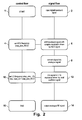
- Fig. 2 shows a flowchart illustrating the way in which a digital baseband signal is converted into an analogue RF signal, and the processing of the signal flow by the up-converter 1 of Fig. 1.
- the method starts with step 1.
- step 2 a digital baseband signal is inputted into the device.
- step 4 the frequency step size of the NCO 6 driving the complex modulator 5 is chosen. This frequency step size is called step_size_NCO.
- step 6 the frequency of the digital baseband signal is shifted with complex modulator 5, whereby the complex modulator 5 is driven by the signal outputted by NCO 6.
- step 8 the intermediate signal is converted into the analogue domain by means of digital-to-analogue converters 9, 9'.
- step 10 In the analogue domain the frequency step size of the LO 15 is set in step 10. This frequency step size is called step_size_LO and is chosen to be larger than step_size_NCO. Hence step_size_LO > step_size_NCO.
- step 12 the analogue signals A 1, A 2 are mixed with the signal of LO 15. This is done in analogue I/Q modulator 10.
- step 14 an analogue RF signal is outputted at port 16, such that the method ends with step 16.
- Steps 2, 6, 8, 12, 14 are steps carried out by the device according to Fig. 1 when processing the signal flow.
- Steps 4 and 10 are settings decided upon by the user of the up-converter, and are in many cases adjusted only once. As a matter of fact, the settings in steps 4 and 10 can each be carried out earlier than just described.
- Fig. 3 shows a flowchart illustrating the way in which an analogue RF signal is converted into a digital baseband signal.
- an analogue RF signal is inputted.
- the frequency step size of an LO driving an I/Q demodulator is chosen. This frequency step size is called step_size_LO.
- the received RF signal is mixed with the signal provided by the LO
- the signal thus obtained is converted into the digital domain by means of two analogue-to-digital converters.
- step 30 the frequency step size of an NCO is set in step 30.
- This frequency step size is called step_size_NCO and is chosen to be smaller than step_size_LO.
- step_size_LO > step_size_NCO.
- step 32 the digital signals are shifted with the signal provided by the NCO. This is done in a complex modulator with a frequency step size step_size_NCO.
- step 34 a digital baseband signal is outputted such that the method ends with step 36.
- Steps 22, 26, 28, 32, 34 are steps carried out by the down-converter when processing the signal flow.
- Steps 24 and 30 are settings decided upon by the user of the up-converter, and are in many cases adjusted only once. As a matter of fact, the settings in steps 24 and 30 can each be carried out earlier than just described.
Landscapes
- Engineering & Computer Science (AREA)
- Power Engineering (AREA)
- Digital Transmission Methods That Use Modulated Carrier Waves (AREA)
Abstract
The invention relates to a method for converting a digital baseband signal into an a-nalogue RF signal or vice versa.
If a digital baseband signal is converted into an analogue RF signal the phase noise and spurious emissions are limiting factors as far as the signal quality is concerned.
It is an object to achieve a signal with low phase noise and no spurious emissions.
It is suggested to convert the signal in the digital domain by a complex modulator and in the analogue domain by an I/Q modulator. As an example, the frequency step size of an NCO driving the complex modulator may be chosen to be smaller than the frequency step size of an LO driving the I/Q modulator.
Description
- The invention relates to the field of telecommunication, and more particularly to oscillator components in telecommunication systems.
- In the framework of wireless telecommunications, and in particular digital wireless communication systems, a baseband signal carrying information has to be modulated to a radio frequency (RF) band prior to broadcasting it into free space.
- The RF band has a predefined bandwidth, e.g. 60 MHz in the case of UMTS. Depending on the broadcasting standard the base stations and users may be distinguished by different radio frequencies. In the case of UMTS the channel width is 5 MHz, and the channels have to be placed within a channel raster of 200 kHz. As a consequence, a transmitter or a receiver must be able to tune the frequency in steps of 200 kHz.
- It is known to use an integer-N PLL synthesizer for the above-mentioned purposes. The integer-N PLL synthesizer provides a good signal quality, albeit with a high phase noise.
- It is further known to substitute the above-mentioned integer-N PLL synthesizer by a fractional-N PLL synthesizer to reduce the phase noise. However, a fractional-N PLL synthesizer shows spurious emissions such that the overall signal quality is worse than in the case of an integer-N PLL.
- It is an object of the invention to provide a method for converting a digital baseband signal into a finely tuned analogue RF signal, whereby the RF signal has a high signal quality. Furthermore, it is an object to provide a method with which an analogue RF signal can be converted into a high-quality digital baseband signal.
- This object and other objects are solved by the features of the independent claims. Preferred embodiments of the invention are described by the features of the dependent claims. It should be emphasized that any reference signs in the claims shall not be construed as limiting the scope of the invention.
- According to a first aspect of the invention a method for converting a digital baseband signal into an analogue RF signal is provided. This method is carried out with a device which will be called up-converter within this description. The up-converter can be an I/Q modulator and a mixer or, as it will be described in the following, a complex modulator and an I/Q modulator. For sake of brevity only the latter possibility will be described in more detail below.
- The up-converter comprises a complex modulator for modulating the digital baseband signal into an intermediate digital baseband signal (low IF-signal; IF=intermediate frequency). The input of the modulator is thus the in-phase signal I and the quadrature component Q of the baseband signal, and its output is a modulated in-phase signal I1 and a modulated quadrature component Q1. The modulator is a complex modulator working in the digital domain. It shifts the frequency spectrum of the baseband signal to a frequency called the intermediate frequency.
- The output signals of the complex modulator are transferred into analogue signals by means of digital-to-analogue converters.
- The analogue signals are then inputted into an I/Q modulator. This I/Q modulator works in the analogue domain and mixes the analogue signals with a frequency provided by a local oscillator. The output of the I/Q modulator is then the output of the up-converter.
- The frequency of the output signal is the sum of the intermediate frequency feeding the complex modulator and of the LO frequency feeding the I/Q modulator:

- The frequency fComplex Modulator which feeds the complex modulator is adjusted with a smaller frequency step size than the frequency f I/Q Modulator which feeds the analogue I/Q modulator. This has the consequence that the precise adjustment of fComplex Modulator is responsible for finely tuning the frequency of the analogue RF signal with frequency fRF signal. Correspondingly, the coarse adjustment of f I/Q Modulator is responsible for coarsely tuning the frequency of the analogue RF signal. As a result the analogue RF signal is finely tuned, whereby the stepping of the tuning of the up-converter is determined by the the frequency step size chosen for adjusting the frequency fComplex Modulator feeding the complex modulator.
- An advantage associated with this embodiment is that the signal quality is very good. The signal has a particularly low phase noise and has no spurious emissions. The reason is that the embodiment reduces the requirements for adjusting the frequency in the I/Q modulator. This leads to less phase noise in the local oscillator feeding the I/Q modulator and thus improves the signal quality of the output signal. This is particularly true when the I/Q modulator is driven by an integer PLL working with large frequency steps.
- In numerical terms the above-mentioned advantage depends on the choice of the local oscillator being part of the I/Q modulator, such that this advantage shall be further explained by assuming that the local oscillator is an Integer-N PLL. If the frequency of the output is 2170 MHz and if a frequency stepping of 200 kHz is desired, the frequency range of 2170 MHz is divided 2170 MHz / 200 kHz = 10.850. This will lead to a degradation in the phase noise of 20 dB * log (10.850) = 80.7 dB inside the PLL loop bandwidth. The signal quality of the Integer-N PLL can be regarded to be good as it has no spurious emissions in contrast to fractional-N PLL's. With the present invention the frequency stepping in the analogue domain can be made wider, e.g. 30 MHz, as a fine tuning of the frequency can be established in the complex modulator. With steps of 30 MHz the degradation of the phase noise is only 20 dB * log (72.3) = 37.2 dB which amounts to an improvement of 43.5 dB in the phase noise without a deterioration of the signal quality.
- It is also possible to modify the steps of the above embodiment and to do the steps of the above embodiment in reverse order, such that a down-conversion is carried out. In this way analogue RF signals are converted into a digital baseband signal. In this second aspect of the invention the RF signal is, as a first step, mixed with the (analogue) signal provided by a local oscillator. The resulting signal is then converted into a digital signal. In the digital domain the frequency spectrum is shifted from an intermediate frequency to baseband. Thereby, a digital baseband signal of high quality is obtained.
- As in the first embodiment, the frequency step size in the digital domain is chosen to be smaller than the frequency step size in the analogue domain. This means that the mixing carried out in the I/Q modulator coarsely tunes the frequency of the baseband signal, and that the shifting in the complex modulator finely tunes the frequency of the baseband signal.
- The output frequency of the up-converter may be in the GHz region, and is preferably between about 0.4 GHz and about 5 GHz. The RF output signal can then be used by transmitters and receivers for wireless communication systems such as GSM systems, UMTS systems, WiMAX systems or the like.
- The method according to
claim 2 can be used by an electronic receiver to receive analogue RF signals and to convert them into a digital baseband signal. Correspondingly, the method ofclaim 1 can be used by an electronic transmitter processing digital baseband signals and transmitting them as analogue RF signals over the air interface. The receiver and the transmitter may be part of a base station of a wireless telecommunication system, e.g. a cellular system, or of a terminal device serviced by a base station of such a telecommunication system. The terminal device may be a mobile terminal device such as a mobile phone, a laptop, a notebook, a digital portable assistant (PDA) or other suitable electronic devices which can be serviced by a base station in a wireless fashion. - The oscillator feeding the complex modulator can be implemented as a NCO (numerically controlled oscillator) or as a CORDIC module. With a CORDIC module the accuracy can be arbitrarily accurate. The local oscillator feeding the analogue I/Q modulator can be implemented as an Integer-N PLL.
- These and other aspects of the invention will be apparent from and elucidated with reference to the embodiments thereafter. It should be noted that the use of reference signs shall not be construed as limiting the scope of the invention.
-
- Fig. 1
- shows an up-converter for converting a digital baseband signal into an analogue signal according to an embodiment of the invention,
- Fig. 2
- shows a flowchart illustrating the way in which a digital baseband signal is, with the help of the device according to Fig. 1, converted into an analogue RF signal,
- Fig. 3
- shows a flowchart illustrating the way in which an analogue RF signal is, with the help of the device according to Fig. 1, converted into a digital baseband signal.
- Fig. 1 shows an embodiment of an up-
converter 1 within a TX-frontend 2. On the lefthandside input ports complex modulator 5. Thecomplex modulator 5 comprises aNCO 6, twoadders 7, 7' and fourmixers complex modulator 5 shifts the digital frequency spectrum of the complex input signal by a fixed frequency set in theNCO 6. The functioning of this complex modulator is well known to the man skilled in the art and thus not discussed any further. - The output I1 and Q1 of
complex modulator 5 are inputted into two digital-to-analogue converters 9 and 9' respectively. - The corresponding analogue signals A1 and A2 are transferred as an input for the analogue I/
Q modulator 10 after passing low pass filters 11 and 11' respectively. I/Q modulator has twomixers 12 and 12', aphase shifter 13 and anadder 14. The functioning of the analogue I/Q modulator 10 is known to the man skilled in the art and thus does not need further explanation. Analogue I/Q modulator 10 mixes complex analogue signals A1 and A2 with the radio frequency of alocal oscillator 15. The local oscillator may be a Integer-N PLL, and may provide a frequency in the range of of 0.4 GHz to 5 GHz. - Fig. 2 shows a flowchart illustrating the way in which a digital baseband signal is converted into an analogue RF signal, and the processing of the signal flow by the up-
converter 1 of Fig. 1. The method starts withstep 1. In step 2 a digital baseband signal is inputted into the device. Instep 4 the frequency step size of theNCO 6 driving thecomplex modulator 5 is chosen. This frequency step size is called step_size_NCO. Instep 6 the frequency of the digital baseband signal is shifted withcomplex modulator 5, whereby thecomplex modulator 5 is driven by the signal outputted byNCO 6. Instep 8 the intermediate signal is converted into the analogue domain by means of digital-to-analogue converters 9, 9'. - In the analogue domain the frequency step size of the
LO 15 is set instep 10. This frequency step size is called step_size_LO and is chosen to be larger than step_size_NCO. Hence step_size_LO > step_size_NCO. Instep 12 the analogue signals A1, A2 are mixed with the signal ofLO 15. This is done in analogue I/Q modulator 10. Instep 14 an analogue RF signal is outputted atport 16, such that the method ends withstep 16. -
Steps Steps steps - Fig. 3 shows a flowchart illustrating the way in which an analogue RF signal is converted into a digital baseband signal. In
step 22 an analogue RF signal is inputted. Instep 24 the frequency step size of an LO driving an I/Q demodulator is chosen. This frequency step size is called step_size_LO. Instep 26 the received RF signal is mixed with the signal provided by the LO Instep 28 the signal thus obtained is converted into the digital domain by means of two analogue-to-digital converters. - In the digital domain the frequency step size of an NCO is set in
step 30. This frequency step size is called step_size_NCO and is chosen to be smaller than step_size_LO. Hence step_size_LO > step_size_NCO. Instep 32 the digital signals are shifted with the signal provided by the NCO. This is done in a complex modulator with a frequency step size step_size_NCO. In step 34 a digital baseband signal is outputted such that the method ends withstep 36. -
Steps Steps steps -
- 01
- Up-converter
- 02
- TX-frontend
- 03
- Input port
- 04
- Input port
- 05
- Complex modulator
- 06
- NCO
- 07
- Adder
- 07'
- Adder
- 08
- Mixer
- 08'
- Mixer
- 08"
- Mixer
- 08"'
- Mixer
- 09
- DAC
- 09'
- DAC
- 10
- I/Q modulator
- 11
- Low pass filter
- 11'
- Low pass filter
- 12
- Mixer
- 12'
- Mixer
- 13
- 90° phase shifter
- 14
- Adder
- 15
- Local oscillator
- 16
- Output port
Claims (4)
- Method of finely tuning the frequency of an analogue radio frequency (RF) signal, the method comprising the following steps:a) shifting the frequency of a baseband signal to an intermediate frequency,b) converting the resulting signal into an analogue signal,c) mixing the analogue signal with a signal provided by a local oscillator (LO), thereby obtaining the RF signal,d) whereby the frequency step size in step a) is chosen to be smaller than the frequency step size in step c).
- Method of finely tuning a radio frequency (RF) signal to a digital baseband signal, the method comprising the following steps:a) mixing an analogue RF signal with the signal provided by a local oscillator,b) converting the resulting signal into a digital signal,c) shifting the frequency of the digital signal from an intermediate frequency to baseband,d) whereby the frequency step size in step c) is chosen to be smaller than the frequency step size in step a).
- Method according to claim 1 or 2, wherein the step size of the intermediate frequency is chosen to be smaller than the frequency step size of the LO.
- Method according to claim 3, wherein the step size of the intermediate frequency is in the kHz region, and whereby the step size of the frequency provided by the local oscillator is in the MHz region.
Priority Applications (1)
| Application Number | Priority Date | Filing Date | Title |
|---|---|---|---|
| EP06290067A EP1811650A1 (en) | 2006-01-10 | 2006-01-10 | Method for finely tuning the frequency of a radio signal |
Applications Claiming Priority (1)
| Application Number | Priority Date | Filing Date | Title |
|---|---|---|---|
| EP06290067A EP1811650A1 (en) | 2006-01-10 | 2006-01-10 | Method for finely tuning the frequency of a radio signal |
Publications (1)
| Publication Number | Publication Date |
|---|---|
| EP1811650A1 true EP1811650A1 (en) | 2007-07-25 |
Family
ID=36681151
Family Applications (1)
| Application Number | Title | Priority Date | Filing Date |
|---|---|---|---|
| EP06290067A Withdrawn EP1811650A1 (en) | 2006-01-10 | 2006-01-10 | Method for finely tuning the frequency of a radio signal |
Country Status (1)
| Country | Link |
|---|---|
| EP (1) | EP1811650A1 (en) |
Cited By (1)
| Publication number | Priority date | Publication date | Assignee | Title |
|---|---|---|---|---|
| EP2388909A1 (en) * | 2010-05-18 | 2011-11-23 | Rohde & Schwarz GmbH & Co. KG | Signal generator with digital intermediate frequency and digital frequency adjustment |
Citations (4)
| Publication number | Priority date | Publication date | Assignee | Title |
|---|---|---|---|---|
| US5548244A (en) * | 1994-11-14 | 1996-08-20 | Hughes Aircraft Company | Method and apparatus for eliminating DC offset for digital I/Q demodulators |
| US20020048325A1 (en) * | 2000-09-21 | 2002-04-25 | Samsung Electronics Co., Ltd. | Digital down-converter |
| EP1213830A1 (en) * | 2000-12-07 | 2002-06-12 | Motorola, Inc. | Multi-mode radio communications device using a common reference oscillator |
| US20020150169A1 (en) * | 2001-04-16 | 2002-10-17 | Samsung Electronics Co., Ltd. | Apparatus and method for measuring propagation delay in an NB-TDD CDMA mobile communication system |
-
2006
- 2006-01-10 EP EP06290067A patent/EP1811650A1/en not_active Withdrawn
Patent Citations (4)
| Publication number | Priority date | Publication date | Assignee | Title |
|---|---|---|---|---|
| US5548244A (en) * | 1994-11-14 | 1996-08-20 | Hughes Aircraft Company | Method and apparatus for eliminating DC offset for digital I/Q demodulators |
| US20020048325A1 (en) * | 2000-09-21 | 2002-04-25 | Samsung Electronics Co., Ltd. | Digital down-converter |
| EP1213830A1 (en) * | 2000-12-07 | 2002-06-12 | Motorola, Inc. | Multi-mode radio communications device using a common reference oscillator |
| US20020150169A1 (en) * | 2001-04-16 | 2002-10-17 | Samsung Electronics Co., Ltd. | Apparatus and method for measuring propagation delay in an NB-TDD CDMA mobile communication system |
Non-Patent Citations (1)
| Title |
|---|
| CROLS J ET AL: "A SINGLE-CHIP 900 MHZ CMOS RECEIVER FRONT-END WITH A HIGH PERFORMANCE LOW-IF TOPOLOGY", IEEE JOURNAL OF SOLID-STATE CIRCUITS, IEEE SERVICE CENTER, PISCATAWAY, NJ, US, vol. 30, no. 12, December 1995 (1995-12-01), pages 1483 - 1492, XP000557254, ISSN: 0018-9200 * |
Cited By (2)
| Publication number | Priority date | Publication date | Assignee | Title |
|---|---|---|---|---|
| EP2388909A1 (en) * | 2010-05-18 | 2011-11-23 | Rohde & Schwarz GmbH & Co. KG | Signal generator with digital intermediate frequency and digital frequency adjustment |
| DE102010027566A1 (en) * | 2010-05-18 | 2011-11-24 | Rohde & Schwarz Gmbh & Co. Kg | Signal generator with digital intermediate frequency and digital fine tuning |
Similar Documents
| Publication | Publication Date | Title |
|---|---|---|
| US6091780A (en) | Transmitting and receiving radio signals | |
| US7327993B2 (en) | Low leakage local oscillator system | |
| US10911087B2 (en) | Receiver and receiving method of receiver | |
| US5983081A (en) | Method for generating frequencies in a direct conversion transceiver of a dual band radio communication system, a direct conversion transceiver of a dual band radio communication system and the use of this method and apparatus in a mobile station | |
| US6658237B1 (en) | Multi-Band transceiver utilizing direct conversion receiver | |
| US20080233892A1 (en) | Method and system for an integrated vco and local oscillator architecture for an integrated fm transmitter and fm receiver | |
| US6828863B2 (en) | Multi-band frequency synthesizer for mobile terminals | |
| US7424271B2 (en) | Multi-mode and multi-band RF transceiver and related communications method | |
| CN101316105A (en) | Multi-standard multi-module wireless transceiver | |
| KR100458715B1 (en) | Arrangement in a communication system | |
| US6816021B2 (en) | Multiple band local oscillator frequency generation circuit | |
| US20020054627A1 (en) | Synthesizer arrangement and a method for generating signals, particularly for a multimode radio telephone device | |
| US6308050B1 (en) | Dual band mobile phone using the same intermediate frequency for both bands | |
| US6850745B2 (en) | Method and apparatus for generating a self-correcting local oscillation | |
| US20030064699A1 (en) | Down-converting multiple received radio frequency signals | |
| EP2371058B1 (en) | Radio receiver | |
| US20080125060A1 (en) | Radio Frequency Transceiver | |
| US6347121B1 (en) | Transmitting and receiving radio signals | |
| US7398074B2 (en) | Integrated transceiver circuit with low interference production and sensitivity | |
| EP1811650A1 (en) | Method for finely tuning the frequency of a radio signal | |
| US6968159B2 (en) | Frequency converter and communication device | |
| GB2427517A (en) | Zero IF (ZIF) dual-conversion receiver | |
| EP1881608A1 (en) | Radio frequency transceiver | |
| HK1104689A (en) | Digital noise coupling reduction and variable intermediate frequency generation in mixed signal circuits |
Legal Events
| Date | Code | Title | Description |
|---|---|---|---|
| PUAI | Public reference made under article 153(3) epc to a published international application that has entered the european phase |
Free format text: ORIGINAL CODE: 0009012 |
|
| AK | Designated contracting states |
Kind code of ref document: A1 Designated state(s): AT BE BG CH CY CZ DE DK EE ES FI FR GB GR HU IE IS IT LI LT LU LV MC NL PL PT RO SE SI SK TR |
|
| AX | Request for extension of the european patent |
Extension state: AL BA HR MK YU |
|
| AKX | Designation fees paid | ||
| STAA | Information on the status of an ep patent application or granted ep patent |
Free format text: STATUS: THE APPLICATION IS DEEMED TO BE WITHDRAWN |
|
| 18D | Application deemed to be withdrawn |
Effective date: 20080126 |
|
| REG | Reference to a national code |
Ref country code: DE Ref legal event code: 8566 |