EP1811564A1 - Electrical fuse device based on a phase-change memory element and corresponding programming method - Google Patents
Electrical fuse device based on a phase-change memory element and corresponding programming method Download PDFInfo
- Publication number
- EP1811564A1 EP1811564A1 EP06425025A EP06425025A EP1811564A1 EP 1811564 A1 EP1811564 A1 EP 1811564A1 EP 06425025 A EP06425025 A EP 06425025A EP 06425025 A EP06425025 A EP 06425025A EP 1811564 A1 EP1811564 A1 EP 1811564A1
- Authority
- EP
- European Patent Office
- Prior art keywords
- terminal
- region
- programming
- fuse
- fuse device
- Prior art date
- Legal status (The legal status is an assumption and is not a legal conclusion. Google has not performed a legal analysis and makes no representation as to the accuracy of the status listed.)
- Granted
Links
Images




Classifications
-
- H—ELECTRICITY
- H10—SEMICONDUCTOR DEVICES; ELECTRIC SOLID-STATE DEVICES NOT OTHERWISE PROVIDED FOR
- H10W—GENERIC PACKAGES, INTERCONNECTIONS, CONNECTORS OR OTHER CONSTRUCTIONAL DETAILS OF DEVICES COVERED BY CLASS H10
- H10W20/00—Interconnections in chips, wafers or substrates
- H10W20/40—Interconnections external to wafers or substrates, e.g. back-end-of-line [BEOL] metallisations or vias connecting to gate electrodes
- H10W20/49—Adaptable interconnections, e.g. fuses or antifuses
- H10W20/493—Fuses, i.e. interconnections changeable from conductive to non-conductive
-
- G—PHYSICS
- G11—INFORMATION STORAGE
- G11C—STATIC STORES
- G11C17/00—Read-only memories programmable only once; Semi-permanent stores, e.g. manually-replaceable information cards
- G11C17/14—Read-only memories programmable only once; Semi-permanent stores, e.g. manually-replaceable information cards in which contents are determined by selectively establishing, breaking or modifying connecting links by permanently altering the state of coupling elements, e.g. PROM
- G11C17/16—Read-only memories programmable only once; Semi-permanent stores, e.g. manually-replaceable information cards in which contents are determined by selectively establishing, breaking or modifying connecting links by permanently altering the state of coupling elements, e.g. PROM using electrically-fusible links
-
- H—ELECTRICITY
- H10—SEMICONDUCTOR DEVICES; ELECTRIC SOLID-STATE DEVICES NOT OTHERWISE PROVIDED FOR
- H10B—ELECTRONIC MEMORY DEVICES
- H10B63/00—Resistance change memory devices, e.g. resistive RAM [ReRAM] devices
- H10B63/30—Resistance change memory devices, e.g. resistive RAM [ReRAM] devices comprising selection components having three or more electrodes, e.g. transistors
-
- H—ELECTRICITY
- H10—SEMICONDUCTOR DEVICES; ELECTRIC SOLID-STATE DEVICES NOT OTHERWISE PROVIDED FOR
- H10N—ELECTRIC SOLID-STATE DEVICES NOT OTHERWISE PROVIDED FOR
- H10N70/00—Solid-state devices having no potential barriers, and specially adapted for rectifying, amplifying, oscillating or switching
- H10N70/20—Multistable switching devices, e.g. memristors
- H10N70/231—Multistable switching devices, e.g. memristors based on solid-state phase change, e.g. between amorphous and crystalline phases, Ovshinsky effect
-
- H—ELECTRICITY
- H10—SEMICONDUCTOR DEVICES; ELECTRIC SOLID-STATE DEVICES NOT OTHERWISE PROVIDED FOR
- H10N—ELECTRIC SOLID-STATE DEVICES NOT OTHERWISE PROVIDED FOR
- H10N70/00—Solid-state devices having no potential barriers, and specially adapted for rectifying, amplifying, oscillating or switching
- H10N70/801—Constructional details of multistable switching devices
- H10N70/821—Device geometry
- H10N70/826—Device geometry adapted for essentially vertical current flow, e.g. sandwich or pillar type devices
-
- H—ELECTRICITY
- H10—SEMICONDUCTOR DEVICES; ELECTRIC SOLID-STATE DEVICES NOT OTHERWISE PROVIDED FOR
- H10N—ELECTRIC SOLID-STATE DEVICES NOT OTHERWISE PROVIDED FOR
- H10N70/00—Solid-state devices having no potential barriers, and specially adapted for rectifying, amplifying, oscillating or switching
- H10N70/801—Constructional details of multistable switching devices
- H10N70/841—Electrodes
- H10N70/8413—Electrodes adapted for resistive heating
-
- H—ELECTRICITY
- H10—SEMICONDUCTOR DEVICES; ELECTRIC SOLID-STATE DEVICES NOT OTHERWISE PROVIDED FOR
- H10N—ELECTRIC SOLID-STATE DEVICES NOT OTHERWISE PROVIDED FOR
- H10N70/00—Solid-state devices having no potential barriers, and specially adapted for rectifying, amplifying, oscillating or switching
- H10N70/801—Constructional details of multistable switching devices
- H10N70/881—Switching materials
- H10N70/882—Compounds of sulfur, selenium or tellurium, e.g. chalcogenides
- H10N70/8828—Tellurides, e.g. GeSbTe
-
- G—PHYSICS
- G11—INFORMATION STORAGE
- G11C—STATIC STORES
- G11C13/00—Digital stores characterised by the use of storage elements not covered by groups G11C11/00, G11C23/00, or G11C25/00
- G11C13/0002—Digital stores characterised by the use of storage elements not covered by groups G11C11/00, G11C23/00, or G11C25/00 using resistive RAM [RRAM] elements
- G11C13/0004—Digital stores characterised by the use of storage elements not covered by groups G11C11/00, G11C23/00, or G11C25/00 using resistive RAM [RRAM] elements comprising amorphous/crystalline phase transition cells
Definitions
- the present invention relates to an electrical fuse device based on a phase-change memory element and to a corresponding programming method, in particular for a read-only memory (ROM) of the one-time-programmable (OTP) type, to which the following description will make reference, without this implying any loss in generality.
- ROM read-only memory
- OTP one-time-programmable
- one-time-programmable ROMs find a wide range of applications for permanent storage of information, or for forming permanent connections within integrated circuits.
- these memories can be used for programming redundant elements in order to replace identical elements that have proven faulty during an electrical testing (operation known as EWS - Electrical Wafer Sorting), prior to carrying out packaging or soldering of the integrated circuits on the board, or else for storage of basic information regarding the integrated circuit, such as identifier codes or calibration information.
- EWS - Electrical Wafer Sorting operation known as EWS - Electrical Wafer Sorting
- the aforesaid information must be stored in a permanent way in order to be recovered after the packaging or soldering operations.
- E 2 PROM devices require oxide layers having a large thickness (for example, 7 nm) to prevent high leakage currents and sustain a charge stored on a corresponding floating terminal.
- the scales of integration required by modern integrated circuits do not always enable use of such large oxide thicknesses.
- the use of E 2 PROM devices in any case involves a high area occupation.
- the fuse devices commonly used for the applications referred to above are programmed using a laser, which is used to cut a connection after the fuse device has been manufactured.
- Laser programming entails an additional process step, extraneous to semiconductor technology, and moreover calls for a perfect alignment of the laser with respect to the fuse device to be programmed.
- Anti-fuse devices are typically based on the perforation of metal-insulator-metal structures to obtain low-resistance paths. Said devices require high programming voltages, and consequently involve high breaking voltages of the programming circuits associated thereto. Furthermore, said devices are generally of a horizontal type and involve a high area occupation.
- Phase-change memories are moreover known, which exploit, for storage of information, the characteristics of materials that have the property of switching between phases having different electrical characteristics. For example, said materials can switch between a disorderly, amorphous phase and an orderly, crystalline or polycrystalline phase, and the two phases are associated to resistivities having considerably different values, and consequently to different values of a stored datum.
- the elements of Group VI of the periodic table such as tellurium (Te), selenium (Se), or antimony (Sb), referred to as calcogenides or calcogenic materials, may advantageously be used to obtain phase-change memory cells.
- the currently most promising calcogenide is formed by an alloy of Ge, Sb and Te, generically referred to as GST (for example, Ge 2 Sb 2 Te 5 ) .
- phase changes are obtained by locally increasing the temperature of the cells of calcogenic material by means of resistive electrodes (generally known as heaters) set in contact with the region of calcogenic material.
- a selection device for example, a MOSFET or a bipolar transistor, is connected to the heater and is configured to enable passage of a programming electrical current through the heater. Said electrical current, by the Joule effect, generates the temperatures necessary for phase change.
- the heaters generally have sublithographic sections (i.e., dimensions smaller than the dimensions that can be achieved with current lithographic techniques, for example smaller than 100 nm, down to approximately 5-20 nm).
- phase-change memory cells A wide range of manufacturing processes have been proposed to obtain phase-change memory cells, and the configurations of the resulting memory cells are different, in particular as regards coupling between the heater and a corresponding calcogenic region.
- a microtrench architecture is described in US 6,891,747
- a lance-shaped or ring-shaped tubular architecture is described in the patent application No. EP 05102811.6, filed on April 8, 2005 .
- PCMs cannot be used in the applications described above.
- the high temperatures that are generated during the processes of packaging or soldering on the board can lead to the change of state of previously programmed memory cells and the consequent loss of the stored information.
- the possibility exists that memory cells in the amorphous state will switch to the crystalline state on account of said high temperatures.
- the aim of the present invention is to provide fuse devices (in particular for one-time-programmable memory elements) that will enable the aforesaid disadvantages and problems to be overcome.
- a fuse device and a method for programming a fuse device are consequently provided, as defined in claims 1 and 15, respectively.
- An aspect of the present invention envisages use of a phase-change memory element to provide a semiconductor fuse device.
- the phase-change memory element is programmed for this purpose in two stable states: a low-resistivity closed state (for example corresponding to a "1"), and an open state (for example corresponding to a "0").
- the open state is obtained by physical breaking of a region of calcogenic material of the phase-change memory element, via application of a given electrical quantity (in particular, via the passage of a high electrical current).
- the information associated to both states are stable and not modifiable, for example by soldering or packaging of a corresponding integrated circuit.
- a fuse device 1 comprises a fuse element 2 (as will be clarified hereinafter, based on a phase-change memory element), and a selector element 3, which is electrically connected to the fuse element 2 and is configured to enable programming of the fuse element 2.
- the selector element 3 illustrated in Figure 1 is an N-channel MOSFET of a planar type. It is clear, however, that other selector elements could be used in an altogether equivalent way, for example any FET (vertical MOSFET, JFET, FinFET, etc.), or else a BJT or a BiFET.
- Figure 1 and the following figures illustrate a phase-change memory element having a microtrench architecture. Once again, it is clear that other structures could be used in an altogether equivalent way, for example of the wall or tubular type.
- the selector element 3 is provided with: a first current-conduction region (in particular, a current-input region), in the example a drain region 4, and a second current-conduction region (in particular, a current-output region), in the example a source region 5, which are formed, in a known way, within a substrate 6 of semiconductor material (in particular silicon); and a control region, in the example, a gate region 7, set above the substrate 6 between the drain region 4 and source region 5, and partially overlapping them.
- a first current-conduction region in particular, a current-input region
- a drain region 4 in the example a drain region 4
- a second current-conduction region in particular, a current-output region
- the aforesaid regions are coated with a respective silicidation region 8, and contact elements 9a, 9b, in particular plugs, made, for example, of tungsten surrounded by a Ti/TiN multilayer, extend vertically with respect to the substrate 6, from the drain region 4 and the source region 5, respectively.
- the fuse element 2 has a vertical structure and comprises a bottom electrode 10, made, for example, of tungsten (W), surrounded by first barrier regions 11, for example constituted by a Ti/TiN multilayer.
- the bottom electrode 10 is made by an end portion of a contact element 9a associated to the drain region 4 of the selector element 3, preferably a contact element arranged in a central position with respect to the drain region 4 so that the fuse element 2 is set above the drain region.
- a heater 12 is placed on, and in contact with, the bottom electrode 10.
- the heater 12, as may be seen in Figure 1, extends along the periphery of an approximately rectangular area, and has a first long portion 12a and a second long portion 12b, and a first short portion 12c and a second short portion 12d, said long portions and short portions being orthogonal to one another.
- Each of said portions 12a-12d (as illustrated for example in the next Figure 10) has a channel-shaped structure, and is made by a metallic coating, for example of TiSiN, which forms respective side walls and a respective bottom surface, and by a dielectric filling material.
- Contact between the bottom electrode 10 and the bottom wall of the heater 12 occurs at a central area of the first long portion 12a of the heater 12.
- the second long portion 12b is instead set outside the drain region 5.
- a phase-change memory element 13 (referred to in what follows as PCM element 13) is set above the heater 12, in particular above the first long portion 12a thereof, in a position vertically corresponding to the bottom electrode 10.
- the PCM element 13 comprises a calcogenic region 15, made of phase-change material, for example GST (Ge 2 Sb 2 Te 5 ), and a second barrier region, made, for example, of Ti/TiN, on the calcogenic region 15.
- the second barrier region constitutes a top electrode 16 of the fuse element 2.
- the PCM element 13 extends longitudinally on an approximately rectangular area (approximately parallel to the first and second short portions 12c, 12d of the heating element 12) crossing the long portion 12a of the heating element 12.
- the PCM element 13 is formed (in a known way) with the microtrench technique, and the calcogenic region 15 contacts the walls of the central area of the first long portion 12a of the heater 12 only at a central depression having a cross section with sublithographic dimensions.
- the area of contact is a storage area 15a (and, as will be clarified hereinafter, an electrically breakable area) of the fuse device 1.
- an insulation region 19 surrounds and electrically insulates the fuse element 2.
- the top electrode 16 is connected to a high-voltage line V cc , for example to the supply line of the fuse device 1, and the source region 5, via the corresponding contact elements 9b, is connected to a reference-voltage line GND of the fuse device 1.
- V cc high-voltage line
- GND reference-voltage line
- the open state of the fuse element 2 is programmed by applying a current and a voltage having a value such as to cause physical breaking of the storage area 15a.
- a programming pulse is applied having a duration, for example, of between 100 ns and 1 ⁇ s, with a current of, for example, 2.5 mA, and a voltage of, for example, 2.5 V.
- said programming pulse causes breaking of the storage area 15a, and creation of a void 20, which interrupts the electrical connection between the top electrode 16 and the bottom electrode 10 of the fuse element 2 (creating the open state, or high-resistance state).
- the void 20 extends in part in the calcogenic region 15 and in part in the heater 12.
- breaking of the storage area 15a is obtained using voltages having a value of between approximately 2 V and 3 V (preferably 2.5 V), and currents having a value of between approximately 2 A and 3 A (preferably 2.5 A).
- the closed state of the fuse element 2 is instead programmed by applying to the storage area 15a a triangular voltage pulse (Figure 6), for example having a duration of 1 ⁇ s and an amplitude of 700 ⁇ A.
- Said pulse causes melting of the calcogenic material (at a temperature of approximately 600°C) and subsequent slow cooling thereof, which leads to its crystallization.
- a single crystallization pulse can be applied, or else a sequence of pulses having decreasing amplitudes.
- the crystallization procedure has a duration of between 1 and 10 ⁇ s.
- ballast effect leads to a greater uniformity of the current distribution, and occurs as the resistance increases along the path of the current.
- the PCM element 13 is arranged above the second long portion 12b of the heater 12 at a distance from the contact elements 9a associated to the drain region 4.
- the electrical contact with the PCM element 13, and in particular with the storage area 15a, is in any case guaranteed by the presence of metallic material on the side walls and on the bottom surface of the heater 12, and by its continuity.
- the heating element represents a series resistance to the passage of the programming current.
- the series resistance in the path of the programming current, and hence the aforesaid ballast effect can be further increased by removing the silicidation regions 8 on the source and drain regions (thus creating an additional series resistance on both the source and drain contacts), and possibly moving the contact elements 9a of the drain region 4 away from the gate region 7 (as indicated by the arrow in the figure).
- the configuration of the fuse device 1 previously described envisages the passage of the programming current in the fuse element 2 from the top electrode 16 to the bottom one 10.
- Experimental tests conducted by the applicant have, however, demonstrated an even better repeatability of the programming operations of the fuse element when the direction of the flow of the programming current is reversed.
- alternative configurations of the fuse device 1 are proposed, which share the feature of envisaging a flow of the programming current from the bottom electrode 10 to the top electrode 16 of the fuse element 2.
- a second embodiment, illustrated in Figures 9 and 10 envisages again the use of a selector element 3 of the planar N-channel MOSFET type, but in this case the bottom electrode 10 of the fuse element 2 is connected to the source region 5 of the selector element 3.
- the selector element 3 has an active area 22, having P-type conductivity, made within the substrate 6 (having a P - doping) and isolated by means of isolation trenches 23, for example using the Shallow-Trench Isolation (STI) technique.
- the drain region 4 and the source region 5 are provided within the active area 22; in detail, the drain region 4 comprises a first drain strip 4a and a second drain strip 4b, which extend in a first direction x parallel to one another, and the source region 5 comprises a source strip extending in the first direction x between the drain strips 4a, 4b.
- electrical contacts 24 illustrated in Figure 9) contact the drain strips 4a, 4b.
- the gate region 7 is constituted by a polysilicon rectangular ring structure, which has long portions set between the drain region and the source region, and short portions, which extend in a second direction y, orthogonal to the first direction x, and are set outside the active area 22, where they are contacted by electrical gate contacts.
- the fuse device 1 comprises two pairs of "dummy" elements 25, arranged laterally to the fuse element 2. Each "dummy" element has the same structure as the fuse element 2, but is not electrically connected and is hence not crossed by current during the programming steps. The presence of the dummy elements 25, however, enables uniform operation of the fuse element 2.
- a contact element 9a associated to the drain region 4, for example a line of tungsten extending in the first direction x, is electrically connected, via the electrical contacts 24, to the high-voltage line V cc (in a way not illustrated), while a contact element 9b, similar to the contact element 9a and associated to the source region 5, is connected to the heater 12 of the fuse element 2 (thus constituting its bottom electrode 10).
- the heater 12 has a rectangular shape, contained in the direction y by the long portions of the gate region 7, and is again constituted by a metallic coating 26, for example of TiSiN, forming respective side walls and a respective bottom surface, and by a dielectric filling material 27.
- the PCM element 13 is set above the heater 12, and has a rectangular shape extending in the second direction y, starting from a central area of the heater 12 towards the second drain strip 4b, overstepping the gate region 7.
- Contact plugs (so-called "vias 0") 28 electrically connect the top electrode 16 to a first metallization 29 (level-1 metal) that runs in the second direction y over the entire active area 22.
- the first metallization 29 is also connected to the reference-voltage line GND of the fuse device 1.
- the programming current flows from the supply line V cc to the drain region 4, and then to the source region 5. From the source region 5 it flows to the bottom electrode 10, and then through the PCM element 13 (and in particular the storage area 15a) to the top electrode 16, up to the reference-voltage line GND.
- the bottom electrode 10 is set at a potential higher than that of the top electrode 16, and, as desired, the current flows from the bottom electrode to the top one.
- Said arrangement is therefore advantageous for improving the repeatability of the programming operations, but feels, however, the body effect occurring in the N-channel MOSFET, due to the voltage increase of the source region 5.
- a third embodiment envisages a configuration substantially similar to the one described with reference to Figures 9-10, with the difference that a P-channel planar MOSFET is used for the selector element 3.
- the active area is constituted by a well 30 of N type within a substrate of P - type, and the drain region 4 and source region 5 are also doped with a P-type doping.
- Said solution has the advantage of not feeling the body effect; however, as is known, the use of P-channel transistors, given the same area occupation, entails the generation of currents of lower value as compared to the use of N-channel transistors.
- a fourth embodiment envisages again the use of a selector element 3 of an N-channel MOSFET type, and at the same time enables elimination of the body effect.
- the drain region 4 and the source region 5 are in this case constituted by respective strips extending in the first direction x, and the gate region 7 is also constituted by a strip, which is set between the source and drain regions and carries respective gate contacts at its ends, outside the active area 22.
- a contact element 9b associated to the source region 5 is connected, via a first plug 32, for example made of tungsten surrounded by a Ti/TiN multilayer, to a first metallization 29, connected in turn to the reference-voltage line GND.
- a contact element 9a associated to the drain region 4 is instead connected, via a second plug 34, to a second metallization 35 (constituting an internal node).
- the second metallization 35 extends in the first direction x, until it reaches the top electrode 16 of the fuse element 2, to which it is connected via a third plug 36 (so-called "via 0").
- connection line 38 for example made of tungsten
- a fourth plug 39 connects the connection line 38 (which also extends in the first direction x) to a third metallization 40, connected to the high-voltage line V cc .
- the programming current flows from the supply line V cc to the connection line 38 (the bottom electrode of the fuse element), then through the PCM element 13 (and in particular the storage area 15a) and the top electrode 16; from this it flows through the second metallization 35 to the drain region 4, then to the source region 5, and finally to the reference-voltage line GND.
- the current flows advantageously from the bottom electrode 10 to the top electrode 16.
- the fuse element 2 is not vertically aligned to one of the current-conduction regions of the selector element 3, as in the preceding solutions, but is shifted laterally (in the second direction y). Said configuration consequently entails a greater area occupation as compared to the preceding solutions. At the same time, it does not feel the body effect, in so far as the source region 5 is connected to the reference-voltage line GND.
- the fuse device 1 can advantageously be used as a memory element of a one-time-programmable ROM storage device 50.
- the ROM storage device 50 comprises a bank of programmable fuses 52 comprising a plurality of fuse devices (each made as described previously), and a purposely provided programming circuit 54, coupled to the bank of programmable fuses 52 to carry out programming thereof.
- the fuse device has reduced costs and area occupation, and small programming times (less than 10 ⁇ s, if both "0" and “1" data are programmed; less than 100 ns if only the "0" datum is programmed, as described hereinafter). Furthermore, it does not require either additional process steps with respect to the classic steps of the semiconductor industry (as, instead, is required for example by the laser-programmed fuses), or thick oxide layers (as, instead, is required by the E 2 PROMs).
- the described structures also have a vertical structure, and a small overall encumbrance.
- the electrical alteration of the fuse device is highly repeatable, thanks to the fact that the area of contact between the PCM element and the heater has small (i.e., sublithographic) dimensions, which are controllable with extreme precision. Said repeatability is further increased in the arrangements envisaging a flow of current in the fuse element 2 from the bottom electrode 10 to the top electrode 16.
- breaking currents and voltages will follow the same scaling law as PCM memory cells (described, for example, in “ Scaling Analysis of Phase-Change Memory Technology", Pirovano et al., IEDM Tech. Dig., pp. 699-702, 2003 ).
- the breaking voltage will remain practically constant, whilst the programming current will decrease linearly as the scale of integration used in the manufacturing process decreases.
- this will enable fuse devices (inclusive of the fuse element and the corresponding selector element) to be made that are increasingly compact with scaling-down of the technology used.
- the programming of the closed state (corresponding to the "1" value) is not strictly necessary in so far as, as is known, storage elements made of virgin calcogenic material are already crystalline (low-resistivity state), and remain crystalline even after operations such as on-board packaging and soldering (consequently, the information associated to the crystalline state is stable).
- programming of the fuse element 2 can be achieved via selector elements different from the ones illustrated (for example using BJTs).
Landscapes
- Design And Manufacture Of Integrated Circuits (AREA)
- Semiconductor Memories (AREA)
Abstract
Description
- The present invention relates to an electrical fuse device based on a phase-change memory element and to a corresponding programming method, in particular for a read-only memory (ROM) of the one-time-programmable (OTP) type, to which the following description will make reference, without this implying any loss in generality.
- As is known, in the manufacturing process of integrated circuits, one-time-programmable ROMs find a wide range of applications for permanent storage of information, or for forming permanent connections within integrated circuits. For example, these memories can be used for programming redundant elements in order to replace identical elements that have proven faulty during an electrical testing (operation known as EWS - Electrical Wafer Sorting), prior to carrying out packaging or soldering of the integrated circuits on the board, or else for storage of basic information regarding the integrated circuit, such as identifier codes or calibration information. In particular, the aforesaid information must be stored in a permanent way in order to be recovered after the packaging or soldering operations.
- In order to produce the aforesaid memories using semiconductor technology, the use of E2PROM (Electrically Erasable Programmable Read-Only Memory) devices, fuse devices and anti-fuse devices has been proposed. However, for reasons that will be briefly set forth, the solutions referred to have some problems that do not make their use totally satisfactory within modern integrated devices.
- In particular, E2PROM devices require oxide layers having a large thickness (for example, 7 nm) to prevent high leakage currents and sustain a charge stored on a corresponding floating terminal. The scales of integration required by modern integrated circuits do not always enable use of such large oxide thicknesses. Furthermore, the use of E2PROM devices in any case involves a high area occupation.
- The fuse devices commonly used for the applications referred to above are programmed using a laser, which is used to cut a connection after the fuse device has been manufactured. Laser programming entails an additional process step, extraneous to semiconductor technology, and moreover calls for a perfect alignment of the laser with respect to the fuse device to be programmed.
- Anti-fuse devices are typically based on the perforation of metal-insulator-metal structures to obtain low-resistance paths. Said devices require high programming voltages, and consequently involve high breaking voltages of the programming circuits associated thereto. Furthermore, said devices are generally of a horizontal type and involve a high area occupation.
- Other types of semiconductor fuse devices that can be electrically altered, for example based on polysilicon resistors, have been proposed, for example in the patent No.
US 6,337.507 and in the patent application No.US 2003/0218492 . However, none of said devices is optimized in terms of costs, manufacturing times, and programming times (which should be as short as possible). - Phase-change memories (PCMs) are moreover known, which exploit, for storage of information, the characteristics of materials that have the property of switching between phases having different electrical characteristics. For example, said materials can switch between a disorderly, amorphous phase and an orderly, crystalline or polycrystalline phase, and the two phases are associated to resistivities having considerably different values, and consequently to different values of a stored datum. Currently, the elements of Group VI of the periodic table, such as tellurium (Te), selenium (Se), or antimony (Sb), referred to as calcogenides or calcogenic materials, may advantageously be used to obtain phase-change memory cells. The currently most promising calcogenide is formed by an alloy of Ge, Sb and Te, generically referred to as GST (for example, Ge2Sb2Te5) .
- The phase changes are obtained by locally increasing the temperature of the cells of calcogenic material by means of resistive electrodes (generally known as heaters) set in contact with the region of calcogenic material. A selection device (for example, a MOSFET or a bipolar transistor), is connected to the heater and is configured to enable passage of a programming electrical current through the heater. Said electrical current, by the Joule effect, generates the temperatures necessary for phase change. In particular, since the minimization of the area of contact between the heater and the region of calcogenic material is a primary requisite in such devices, in order to ensure repeatability of the programming operations, the heaters generally have sublithographic sections (i.e., dimensions smaller than the dimensions that can be achieved with current lithographic techniques, for example smaller than 100 nm, down to approximately 5-20 nm).
- A wide range of manufacturing processes have been proposed to obtain phase-change memory cells, and the configurations of the resulting memory cells are different, in particular as regards coupling between the heater and a corresponding calcogenic region. For example, a microtrench architecture is described in
US 6,891,747 , while a lance-shaped or ring-shaped tubular architecture is described in the patent application No.EP 05102811.6, filed on April 8, 2005 - Although advantageous as regards performance and manufacturing costs, PCMs cannot be used in the applications described above. In fact, the high temperatures that are generated during the processes of packaging or soldering on the board can lead to the change of state of previously programmed memory cells and the consequent loss of the stored information. In particular, the possibility exists that memory cells in the amorphous state will switch to the crystalline state on account of said high temperatures.
- The aim of the present invention is to provide fuse devices (in particular for one-time-programmable memory elements) that will enable the aforesaid disadvantages and problems to be overcome.
- According to the present invention, a fuse device and a method for programming a fuse device are consequently provided, as defined in
claims - For a better understanding of the present invention, preferred embodiments thereof are now described, purely by way of nonlimiting example and with reference to the attached plate of drawings, wherein:
- Figure 1 is a schematic top plan view of a semiconductor fuse device according to a first embodiment of the present invention, with parts removed for greater clarity;
- Figure 2 is a cross-sectional view of a portion of the fuse device of Figure 1 taken along the line II-II, in which a phase-change fuse element is illustrated, in a first operating condition;
- Figure 3 is a view similar to that of Figure 2 regarding a second operating condition of the phase-change fuse element;
- Figures 4-6 show graphs regarding electrical quantities associated to the fuse element of Figures 2 and 3;
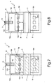
- Figure 7 is a view similar to that of Figure 1, illustrating a variant of the fuse device;
- Figure 8 is a view similar to that of Figure 7, illustrating a further variant of the fuse device;
- Figure 9 is a top-plan view of a second embodiment of the fuse device; and
- Figure 10 is a cross-sectional view of the fuse device of Figure 9, taken along the line X-X;
- Figure 11 is a top-plan view of a third embodiment of the fuse device;
- Figure 12 shows a cross-sectional view of the fuse device of Figure 11, taken along the line XII-XII ;
- Figure 13 is a top-plan view of a fourth embodiment of the fuse device;
- Figure 14 shows a cross-sectional view of the fuse device of Figure 13, taken along the line XIV-XIV; and
- Figure 15 shows a simplified block diagram of a one-time-programmable storage device.
- An aspect of the present invention envisages use of a phase-change memory element to provide a semiconductor fuse device. The phase-change memory element is programmed for this purpose in two stable states: a low-resistivity closed state (for example corresponding to a "1"), and an open state (for example corresponding to a "0"). In particular, the open state is obtained by physical breaking of a region of calcogenic material of the phase-change memory element, via application of a given electrical quantity (in particular, via the passage of a high electrical current). In this manner, the information associated to both states are stable and not modifiable, for example by soldering or packaging of a corresponding integrated circuit.
- In detail, and as illustrated in Figures 1 and 2, a
fuse device 1 according to a first embodiment of the present invention, comprises a fuse element 2 (as will be clarified hereinafter, based on a phase-change memory element), and aselector element 3, which is electrically connected to thefuse element 2 and is configured to enable programming of thefuse element 2. In particular, by way of example, theselector element 3 illustrated in Figure 1 is an N-channel MOSFET of a planar type. It is clear, however, that other selector elements could be used in an altogether equivalent way, for example any FET (vertical MOSFET, JFET, FinFET, etc.), or else a BJT or a BiFET. Furthermore, Figure 1 and the following figures illustrate a phase-change memory element having a microtrench architecture. Once again, it is clear that other structures could be used in an altogether equivalent way, for example of the wall or tubular type. - In detail, the
selector element 3 is provided with: a first current-conduction region (in particular, a current-input region), in the example adrain region 4, and a second current-conduction region (in particular, a current-output region), in the example asource region 5, which are formed, in a known way, within asubstrate 6 of semiconductor material (in particular silicon); and a control region, in the example, agate region 7, set above thesubstrate 6 between thedrain region 4 andsource region 5, and partially overlapping them. The aforesaid regions are coated with arespective silicidation region 8, andcontact elements substrate 6, from thedrain region 4 and thesource region 5, respectively. - As illustrated in detail in Figure 2, the
fuse element 2 has a vertical structure and comprises abottom electrode 10, made, for example, of tungsten (W), surrounded byfirst barrier regions 11, for example constituted by a Ti/TiN multilayer. In particular, thebottom electrode 10 is made by an end portion of acontact element 9a associated to thedrain region 4 of theselector element 3, preferably a contact element arranged in a central position with respect to thedrain region 4 so that thefuse element 2 is set above the drain region. - A
heater 12 is placed on, and in contact with, thebottom electrode 10. Theheater 12, as may be seen in Figure 1, extends along the periphery of an approximately rectangular area, and has a firstlong portion 12a and a secondlong portion 12b, and a firstshort portion 12c and a secondshort portion 12d, said long portions and short portions being orthogonal to one another. Each of saidportions 12a-12d (as illustrated for example in the next Figure 10) has a channel-shaped structure, and is made by a metallic coating, for example of TiSiN, which forms respective side walls and a respective bottom surface, and by a dielectric filling material. Contact between thebottom electrode 10 and the bottom wall of theheater 12 occurs at a central area of the firstlong portion 12a of theheater 12. The secondlong portion 12b is instead set outside thedrain region 5. - A phase-change memory element 13 (referred to in what follows as PCM element 13) is set above the
heater 12, in particular above the firstlong portion 12a thereof, in a position vertically corresponding to thebottom electrode 10. In detail, thePCM element 13 comprises acalcogenic region 15, made of phase-change material, for example GST (Ge2Sb2Te5), and a second barrier region, made, for example, of Ti/TiN, on thecalcogenic region 15. In particular, the second barrier region constitutes atop electrode 16 of thefuse element 2. ThePCM element 13 extends longitudinally on an approximately rectangular area (approximately parallel to the first and secondshort portions long portion 12a of theheating element 12. Moreover, thePCM element 13 is formed (in a known way) with the microtrench technique, and thecalcogenic region 15 contacts the walls of the central area of the firstlong portion 12a of theheater 12 only at a central depression having a cross section with sublithographic dimensions. The area of contact is astorage area 15a (and, as will be clarified hereinafter, an electrically breakable area) of thefuse device 1. Aclosing region 17, made, for example, of silicon nitride, surrounds thePCM element 13 and covers theheater 12 at the top. In addition, aninsulation region 19 surrounds and electrically insulates thefuse element 2. - In use, via purposely provided electrical contacts (not illustrated), the
top electrode 16 is connected to a high-voltage line Vcc, for example to the supply line of thefuse device 1, and thesource region 5, via thecorresponding contact elements 9b, is connected to a reference-voltage line GND of thefuse device 1. When enabled by a control signal supplied to thegate region 7, a programming current consequently passes through thefuse element 2 from thetop electrode 16 to thebottom electrode 10, traversing thecalcogenic region 15 and thestorage area 15a, and then flows through theselector element 3 from thedrain region 4 to thesource region 5. - According to an aspect of the present invention, the open state of the
fuse element 2 is programmed by applying a current and a voltage having a value such as to cause physical breaking of thestorage area 15a. For this purpose, a programming pulse is applied having a duration, for example, of between 100 ns and 1 µs, with a current of, for example, 2.5 mA, and a voltage of, for example, 2.5 V. As illustrated in Figure 3, said programming pulse causes breaking of thestorage area 15a, and creation of a void 20, which interrupts the electrical connection between thetop electrode 16 and thebottom electrode 10 of the fuse element 2 (creating the open state, or high-resistance state). In detail, the void 20 extends in part in thecalcogenic region 15 and in part in theheater 12. As illustrated in Figures 4 and 5, relating to experimental tests conducted by the applicant with afuse device 1 built with a 180-nm technology and with programming pulses of 300 ns, breaking of thestorage area 15a is obtained using voltages having a value of between approximately 2 V and 3 V (preferably 2.5 V), and currents having a value of between approximately 2 A and 3 A (preferably 2.5 A). - The closed state of the
fuse element 2 is instead programmed by applying to thestorage area 15a a triangular voltage pulse (Figure 6), for example having a duration of 1 µs and an amplitude of 700 µA. Said pulse causes melting of the calcogenic material (at a temperature of approximately 600°C) and subsequent slow cooling thereof, which leads to its crystallization. Alternatively, a single crystallization pulse can be applied, or else a sequence of pulses having decreasing amplitudes. Typically, the crystallization procedure has a duration of between 1 and 10 µs. - Given the high values of current required in the breaking operations of the
fuse device 1, a further aspect of the present invention envisages exploitation of the so-called "ballast" effect to prevent the known effects of "crowding" of the current and of thermal "run-away" of theselector element 3. In a per se known manner, the ballast effect leads to a greater uniformity of the current distribution, and occurs as the resistance increases along the path of the current. - For the above purpose (see Figure 7), according to a first variant, the
PCM element 13 is arranged above the secondlong portion 12b of theheater 12 at a distance from thecontact elements 9a associated to thedrain region 4. The electrical contact with thePCM element 13, and in particular with thestorage area 15a, is in any case guaranteed by the presence of metallic material on the side walls and on the bottom surface of theheater 12, and by its continuity. However, advantageously, the heating element represents a series resistance to the passage of the programming current. - According to a further variant (illustrated in Figure 8), the series resistance in the path of the programming current, and hence the aforesaid ballast effect, can be further increased by removing the
silicidation regions 8 on the source and drain regions (thus creating an additional series resistance on both the source and drain contacts), and possibly moving thecontact elements 9a of thedrain region 4 away from the gate region 7 (as indicated by the arrow in the figure). - In any case, the configuration of the
fuse device 1 previously described envisages the passage of the programming current in thefuse element 2 from thetop electrode 16 to thebottom one 10. Experimental tests conducted by the applicant have, however, demonstrated an even better repeatability of the programming operations of the fuse element when the direction of the flow of the programming current is reversed. For this purpose, according to further embodiments of the present invention, alternative configurations of thefuse device 1 are proposed, which share the feature of envisaging a flow of the programming current from thebottom electrode 10 to thetop electrode 16 of thefuse element 2. - A second embodiment, illustrated in Figures 9 and 10, envisages again the use of a
selector element 3 of the planar N-channel MOSFET type, but in this case thebottom electrode 10 of thefuse element 2 is connected to thesource region 5 of theselector element 3. - In detail, the
selector element 3 has anactive area 22, having P-type conductivity, made within the substrate 6 (having a P- doping) and isolated by means ofisolation trenches 23, for example using the Shallow-Trench Isolation (STI) technique. Thedrain region 4 and thesource region 5 are provided within theactive area 22; in detail, thedrain region 4 comprises afirst drain strip 4a and asecond drain strip 4b, which extend in a first direction x parallel to one another, and thesource region 5 comprises a source strip extending in the first direction x between the drain strips 4a, 4b. In addition, electrical contacts 24 (illustrated in Figure 9) contact the drain strips 4a, 4b. Thegate region 7 is constituted by a polysilicon rectangular ring structure, which has long portions set between the drain region and the source region, and short portions, which extend in a second direction y, orthogonal to the first direction x, and are set outside theactive area 22, where they are contacted by electrical gate contacts. In addition to thefuse element 2, thefuse device 1 comprises two pairs of "dummy"elements 25, arranged laterally to thefuse element 2. Each "dummy" element has the same structure as thefuse element 2, but is not electrically connected and is hence not crossed by current during the programming steps. The presence of thedummy elements 25, however, enables uniform operation of thefuse element 2. - With reference in particular to Figure 10, a
contact element 9a, associated to thedrain region 4, for example a line of tungsten extending in the first direction x, is electrically connected, via theelectrical contacts 24, to the high-voltage line Vcc (in a way not illustrated), while acontact element 9b, similar to thecontact element 9a and associated to thesource region 5, is connected to theheater 12 of the fuse element 2 (thus constituting its bottom electrode 10). In particular, theheater 12 has a rectangular shape, contained in the direction y by the long portions of thegate region 7, and is again constituted by ametallic coating 26, for example of TiSiN, forming respective side walls and a respective bottom surface, and by adielectric filling material 27. ThePCM element 13 is set above theheater 12, and has a rectangular shape extending in the second direction y, starting from a central area of theheater 12 towards thesecond drain strip 4b, overstepping thegate region 7. Contact plugs (so-called "vias 0") 28 electrically connect thetop electrode 16 to a first metallization 29 (level-1 metal) that runs in the second direction y over the entireactive area 22. Thefirst metallization 29 is also connected to the reference-voltage line GND of thefuse device 1. - In use, the programming current flows from the supply line Vcc to the
drain region 4, and then to thesource region 5. From thesource region 5 it flows to thebottom electrode 10, and then through the PCM element 13 (and in particular thestorage area 15a) to thetop electrode 16, up to the reference-voltage line GND. In particular, thebottom electrode 10 is set at a potential higher than that of thetop electrode 16, and, as desired, the current flows from the bottom electrode to the top one. - Said arrangement is therefore advantageous for improving the repeatability of the programming operations, but feels, however, the body effect occurring in the N-channel MOSFET, due to the voltage increase of the
source region 5. - To solve the above problem, a third embodiment (Figures 11-12), envisages a configuration substantially similar to the one described with reference to Figures 9-10, with the difference that a P-channel planar MOSFET is used for the
selector element 3. In this case, the active area is constituted by a well 30 of N type within a substrate of P- type, and thedrain region 4 andsource region 5 are also doped with a P-type doping. Said solution has the advantage of not feeling the body effect; however, as is known, the use of P-channel transistors, given the same area occupation, entails the generation of currents of lower value as compared to the use of N-channel transistors. - A fourth embodiment (illustrated in Figures 13-14) envisages again the use of a
selector element 3 of an N-channel MOSFET type, and at the same time enables elimination of the body effect. - In detail, the
drain region 4 and thesource region 5 are in this case constituted by respective strips extending in the first direction x, and thegate region 7 is also constituted by a strip, which is set between the source and drain regions and carries respective gate contacts at its ends, outside theactive area 22. - As illustrated in detail in Figure 14, a
contact element 9b associated to thesource region 5 is connected, via afirst plug 32, for example made of tungsten surrounded by a Ti/TiN multilayer, to afirst metallization 29, connected in turn to the reference-voltage line GND. Acontact element 9a associated to thedrain region 4 is instead connected, via asecond plug 34, to a second metallization 35 (constituting an internal node). Thesecond metallization 35 extends in the first direction x, until it reaches thetop electrode 16 of thefuse element 2, to which it is connected via a third plug 36 (so-called "via 0"). The bottom electrode of thefuse element 2 is instead connected to aconnection line 38, for example made of tungsten, provided above thesubstrate 6, in a position corresponding to anisolation trench 23. Afourth plug 39 connects the connection line 38 (which also extends in the first direction x) to athird metallization 40, connected to the high-voltage line Vcc. - In use, the programming current flows from the supply line Vcc to the connection line 38 (the bottom electrode of the fuse element), then through the PCM element 13 (and in particular the
storage area 15a) and thetop electrode 16; from this it flows through thesecond metallization 35 to thedrain region 4, then to thesource region 5, and finally to the reference-voltage line GND. In particular, also in this case, the current flows advantageously from thebottom electrode 10 to thetop electrode 16. - According to said configuration, the
fuse element 2 is not vertically aligned to one of the current-conduction regions of theselector element 3, as in the preceding solutions, but is shifted laterally (in the second direction y). Said configuration consequently entails a greater area occupation as compared to the preceding solutions. At the same time, it does not feel the body effect, in so far as thesource region 5 is connected to the reference-voltage line GND. - As illustrated in Figure 15, the
fuse device 1 can advantageously be used as a memory element of a one-time-programmableROM storage device 50. In particular, theROM storage device 50 comprises a bank ofprogrammable fuses 52 comprising a plurality of fuse devices (each made as described previously), and a purposely providedprogramming circuit 54, coupled to the bank ofprogrammable fuses 52 to carry out programming thereof. - The advantages of the fuse device and of the corresponding programming method are clear from the foregoing description.
- In any case, it is emphasized that the fuse device has reduced costs and area occupation, and small programming times (less than 10 µs, if both "0" and "1" data are programmed; less than 100 ns if only the "0" datum is programmed, as described hereinafter). Furthermore, it does not require either additional process steps with respect to the classic steps of the semiconductor industry (as, instead, is required for example by the laser-programmed fuses), or thick oxide layers (as, instead, is required by the E2PROMs). The described structures also have a vertical structure, and a small overall encumbrance.
- The electrical alteration of the fuse device is highly repeatable, thanks to the fact that the area of contact between the PCM element and the heater has small (i.e., sublithographic) dimensions, which are controllable with extreme precision. Said repeatability is further increased in the arrangements envisaging a flow of current in the
fuse element 2 from thebottom electrode 10 to thetop electrode 16. - Amongst the various embodiments described, particularly advantageous is the one that envisages the use of a P-channel selector transistor.
- Furthermore, tests conducted by the applicant have demonstrated the capability of the fuse device to maintain the programmed data, even after baking at 250°C for 24 hours.
- In addition, it is reasonable to expect that the breaking currents and voltages will follow the same scaling law as PCM memory cells (described, for example, in "Scaling Analysis of Phase-Change Memory Technology", Pirovano et al., IEDM Tech. Dig., pp. 699-702, 2003). In particular, the breaking voltage will remain practically constant, whilst the programming current will decrease linearly as the scale of integration used in the manufacturing process decreases. Advantageously, this will enable fuse devices (inclusive of the fuse element and the corresponding selector element) to be made that are increasingly compact with scaling-down of the technology used.
- Finally, it is clear that modifications and variations can be made to what is described and illustrated herein, without thereby departing from the scope of the present invention, as defined in the annexed claims.
- In particular, the programming of the closed state (corresponding to the "1" value) is not strictly necessary in so far as, as is known, storage elements made of virgin calcogenic material are already crystalline (low-resistivity state), and remain crystalline even after operations such as on-board packaging and soldering (consequently, the information associated to the crystalline state is stable). However, it may be advantageous to program, as described previously, also the closed state, to obtain higher values of conductivity (and so facilitate the operations of reading, for example using sense amplifiers).
- Finally, it is emphasized that programming of the
fuse element 2 can be achieved via selector elements different from the ones illustrated (for example using BJTs).
Claims (19)
- A fuse device (1) comprising a fuse element (2) having a first terminal (10) and a second terminal (16), and an electrically breakable region (15a) arranged between said first and second terminals (10, 16) and configured to undergo breaking as a result of the supply of a programming electrical quantity,
characterized in that said electrically breakable region (15a) comprises phase-change material. - The fuse device according to claim 1, wherein said phase-change material is a calcogenic material, in particular GST.
- The fuse device according to claim 1 or 2, wherein said fuse element (2) comprises a heating element (12) of conductive material in contact with said first terminal (10), and a phase-change region (15) arranged between said heating element (12) and said second terminal (16); said electrically breakable region (15a) being arranged at the area of contact between said heating element (12) and said phase-change region (15).
- The fuse device according to claim 3, further comprising a selector element (3) electrically connected to said fuse element (2) and configured to enable the supply of said programming electrical quantity to said fuse element (2); in particular, said selector element (3) being a transistor element having a current input terminal (4) and a current output terminal (5) .
- The fuse device according to claim 4, wherein said selector element (3) is configured to enable supply to said electrically breakable region (15a) of a programming pulse with a current comprised between 2 A and 3 A, a voltage comprised between 2 V and 3 V, and a duration comprised between 100 ns and 1 µs.
- The fuse device according to claim 4 or 5, wherein said heating element (12) has a rectangular ring shape having a first long side (12a) and a second long side (12b) including conductive material, said first long side (12a) being arranged above said selector element (3) and said second long side (12b) being arranged outside said selector element (3); and wherein said electrically breakable region (15a) is in contact with said second long side (12b), and said current input terminal (4) is connected to said first long side (12a).
- The fuse device according to claim 4 or 5, wherein said first terminal (10) is connected to said current output terminal (5), said second terminal (16) is connected to a first line (GND) set at a first potential, and said current input terminal (4) is connected to a second line (Vcc) set at a second potential, higher than said first potential.
- The fuse device according to claim 7, wherein said selector element (3) is a P-channel planar MOSFET.
- The fuse device according to claim 4 or 5, wherein said current input terminal (4) is connected to said second terminal (16), said current output terminal (5) is connected to a first line (GND) set at a first potential, and said first terminal (10) is connected to a second line (Vcc) set at a second potential, higher than said first potential.
- The fuse device according to claim 9, wherein said selector element (3) is formed in a substrate (6) of semiconductor material, and said first terminal (10) is in contact with a first connection line (38) provided above said substrate (6), further comprising: first contact elements (34) connecting said current input terminal (4) to a second connection line (35) of conductive material; second contact elements (36) connecting said second connection line (35) to said second terminal (16); and third contact elements (39) connecting said first connection line (38) to said second line (Vcc).
- The fuse device according to any one of the preceding claims, wherein said fuse element (2) has a vertical structure, and said electrically breakable region (15a) has a cross section with sublithographic dimensions.
- The fuse device according to any one of the preceding claims, wherein, in at least one operating condition, said first terminal (10) has a voltage higher than that of said second terminal (16), and said programming electrical quantity comprises a programming current flowing from said first terminal (10) to said second terminal (16).
- A one-time-programmable storage device (50), comprising at least one fuse device (1) according to any one of the preceding claims.
- The storage device according to claim 13, further comprising a programming circuit (54) configured to supply to said fuse device (1) said programming electrical quantity.
- A method for programming a fuse device (1) provided with a fuse element (2) having a first terminal (10) and a second terminal (16), and an electrically breakable region (15a) arranged between said first and second terminals (10, 16), comprising breaking said electrically breakable region (15a),
characterized in that said electrically breakable region (15a) comprises phase-change material, and breaking of said electrically breakable region (15a) comprises supplying to said phase-change material a programming electrical quantity such as to cause breaking thereof. - The method according to claim 15, wherein supplying a programming electrical quantity comprises supplying to said phase-change region (15a) a programming pulse with a current comprised between 2 A and 3 A, a voltage comprised between 2 V and 3 V, and a duration comprised between 100 ns and 1 µs.
- The method according to claim 15 or 16, wherein said fuse element (2) comprises a heating element (12) of conductive material in contact with said first terminal (10), and a phase-change region (15) arranged between said heating element (12) and said second terminal (16), said electrically breakable region (15a) being arranged at the area of contact between said heating element (12) and said phase-change region (15); and wherein supplying a programming electrical quantity comprises supplying a programming current flowing from said first terminal (10) to said second terminal (16) so as to form a void (20) in said electrically breakable region (15a).
- The method according to any one of claims 15-17, further comprising programming said electrically breakable region (15a) in a first low-resistivity operating condition, so as to electrically connect said first and second terminals (10, 16), and programming said electrically breakable region (15a) in a second high-resistivity operating condition, so as to electrically disconnect said first terminal (10) from said second terminal (16); programming in said second high-resistivity operating condition comprising said step of breaking said electrically breakable region (15a).
- A process for manufacturing a fuse device (1), comprising:- forming a first terminal (10) and a second terminal (16); and- forming an electrically breakable region (15a) between said first terminal (10) and said second terminal (16),characterized in that forming an electrically breakable region (15a) comprises forming a region of phase-change material.
Priority Applications (4)
| Application Number | Priority Date | Filing Date | Title |
|---|---|---|---|
| DE602006012793T DE602006012793D1 (en) | 2006-01-20 | 2006-01-20 | Electric fuse structure based on a phase change memory element and corresponding programming method |
| EP06425025A EP1811564B1 (en) | 2006-01-20 | 2006-01-20 | Electrical fuse device based on a phase-change memory element and corresponding programming method |
| US11/625,178 US20070189053A1 (en) | 2006-01-20 | 2007-01-19 | Electrical fuse device based on a phase-change memory element and corresponding programming method |
| US13/212,080 US8410527B2 (en) | 2006-01-20 | 2011-08-17 | Electrical fuse device based on a phase-change memory element and corresponding programming method |
Applications Claiming Priority (1)
| Application Number | Priority Date | Filing Date | Title |
|---|---|---|---|
| EP06425025A EP1811564B1 (en) | 2006-01-20 | 2006-01-20 | Electrical fuse device based on a phase-change memory element and corresponding programming method |
Publications (2)
| Publication Number | Publication Date |
|---|---|
| EP1811564A1 true EP1811564A1 (en) | 2007-07-25 |
| EP1811564B1 EP1811564B1 (en) | 2010-03-10 |
Family
ID=36581783
Family Applications (1)
| Application Number | Title | Priority Date | Filing Date |
|---|---|---|---|
| EP06425025A Expired - Lifetime EP1811564B1 (en) | 2006-01-20 | 2006-01-20 | Electrical fuse device based on a phase-change memory element and corresponding programming method |
Country Status (3)
| Country | Link |
|---|---|
| US (2) | US20070189053A1 (en) |
| EP (1) | EP1811564B1 (en) |
| DE (1) | DE602006012793D1 (en) |
Cited By (2)
| Publication number | Priority date | Publication date | Assignee | Title |
|---|---|---|---|---|
| EP2045814A1 (en) * | 2007-10-03 | 2009-04-08 | STMicroelectronics S.r.l. | Method and device for irreversibly programming and reading nonvolatile memory cells |
| US9263218B2 (en) | 2014-05-23 | 2016-02-16 | Nuvoton Technology Corporation | Variable resistance memory cell based electrically resettable fuse device |
Families Citing this family (23)
| Publication number | Priority date | Publication date | Assignee | Title |
|---|---|---|---|---|
| KR100875165B1 (en) * | 2007-07-04 | 2008-12-22 | 주식회사 동부하이텍 | Semiconductor device and manufacturing method |
| KR20090084531A (en) | 2008-02-01 | 2009-08-05 | 삼성전자주식회사 | Fuse circuit and semiconductor memory device including same |
| KR100985184B1 (en) * | 2008-07-23 | 2010-10-05 | 삼성전자주식회사 | Electrical element and its formation method |
| US8558654B2 (en) | 2008-09-17 | 2013-10-15 | Stmicroelectronics (Grenoble 2) Sas | Vialess integration for dual thin films—thin film resistor and heater |
| US8242876B2 (en) * | 2008-09-17 | 2012-08-14 | Stmicroelectronics, Inc. | Dual thin film precision resistance trimming |
| US8786396B2 (en) | 2008-09-17 | 2014-07-22 | Stmicroelectronics Pte. Ltd. | Heater design for heat-trimmed thin film resistors |
| US8569734B2 (en) | 2010-08-04 | 2013-10-29 | Micron Technology, Inc. | Forming resistive random access memories together with fuse arrays |
| US8659085B2 (en) | 2010-08-24 | 2014-02-25 | Stmicroelectronics Pte Ltd. | Lateral connection for a via-less thin film resistor |
| US8400257B2 (en) | 2010-08-24 | 2013-03-19 | Stmicroelectronics Pte Ltd | Via-less thin film resistor with a dielectric cap |
| US8436426B2 (en) | 2010-08-24 | 2013-05-07 | Stmicroelectronics Pte Ltd. | Multi-layer via-less thin film resistor |
| US8927909B2 (en) | 2010-10-11 | 2015-01-06 | Stmicroelectronics, Inc. | Closed loop temperature controlled circuit to improve device stability |
| US8809861B2 (en) | 2010-12-29 | 2014-08-19 | Stmicroelectronics Pte Ltd. | Thin film metal-dielectric-metal transistor |
| US9159413B2 (en) | 2010-12-29 | 2015-10-13 | Stmicroelectronics Pte Ltd. | Thermo programmable resistor based ROM |
| US8981527B2 (en) * | 2011-08-23 | 2015-03-17 | United Microelectronics Corp. | Resistor and manufacturing method thereof |
| US8526214B2 (en) | 2011-11-15 | 2013-09-03 | Stmicroelectronics Pte Ltd. | Resistor thin film MTP memory |
| US9001550B2 (en) * | 2012-04-27 | 2015-04-07 | Macronix International Co., Ltd. | Blocking current leakage in a memory array |
| US8923666B2 (en) | 2012-05-16 | 2014-12-30 | International Business Machines Corporation | Electrically controlled optical fuse and method of fabrication |
| DE102012210124A1 (en) * | 2012-06-15 | 2013-12-19 | Robert Bosch Gmbh | Composite component and method for producing a composite component |
| US9129964B2 (en) | 2013-04-26 | 2015-09-08 | International Business Machines Corporation | Programmable electrical fuse |
| US9793378B2 (en) | 2013-05-31 | 2017-10-17 | Stmicroelectronics, Inc. | Fin field effect transistor device with reduced overlap capacitance and enhanced mechanical stability |
| US9337143B2 (en) | 2014-01-27 | 2016-05-10 | Globalfoundries Inc. | E-fuse structure with methods of fusing the same and monitoring material leakage |
| WO2018183883A1 (en) * | 2017-03-30 | 2018-10-04 | Massachusetts Institute Of Technology | Gsst and applications in optical devices |
| EP3746843A4 (en) | 2018-01-31 | 2022-02-23 | Massachusetts Institute of Technology | METHODS AND APPARATUS FOR MODULATING LIGHT WITH PHASE CHANGE MATERIALS |
Citations (4)
| Publication number | Priority date | Publication date | Assignee | Title |
|---|---|---|---|---|
| WO2003021675A2 (en) * | 2001-08-30 | 2003-03-13 | Bae Systems Information And Electronics Systems Integration Inc. | Method for manufacturing a programmable chalcogenide fuse within a semiconductor device |
| US6579760B1 (en) * | 2002-03-28 | 2003-06-17 | Macronix International Co., Ltd. | Self-aligned, programmable phase change memory |
| WO2004030033A2 (en) * | 2002-09-25 | 2004-04-08 | Ovonyx, Inc. | Method of operating programmable resistant element |
| WO2006031503A1 (en) * | 2004-09-10 | 2006-03-23 | Intel Corporation | One time programmable phase change memory |
Family Cites Families (9)
| Publication number | Priority date | Publication date | Assignee | Title |
|---|---|---|---|---|
| US6337507B1 (en) * | 1995-09-29 | 2002-01-08 | Intel Corporation | Silicide agglomeration fuse device with notches to enhance programmability |
| US6545903B1 (en) * | 2001-12-17 | 2003-04-08 | Texas Instruments Incorporated | Self-aligned resistive plugs for forming memory cell with phase change material |
| DE60137788D1 (en) * | 2001-12-27 | 2009-04-09 | St Microelectronics Srl | Architecture of a non-volatile phase change memory matrix |
| US6891747B2 (en) * | 2002-02-20 | 2005-05-10 | Stmicroelectronics S.R.L. | Phase change memory cell and manufacturing method thereof using minitrenches |
| KR100437458B1 (en) * | 2002-05-07 | 2004-06-23 | 삼성전자주식회사 | Phase change memory cells and methods of fabricating the same |
| US6903598B2 (en) * | 2002-05-24 | 2005-06-07 | Intel Corporation | Static, low-voltage fuse-based cell with high-voltage programming |
| US6744088B1 (en) * | 2002-12-13 | 2004-06-01 | Intel Corporation | Phase change memory device on a planar composite layer |
| KR100733147B1 (en) * | 2004-02-25 | 2007-06-27 | 삼성전자주식회사 | Phase change memory device and manufacturing method thereof |
| EP1710807B1 (en) * | 2005-04-08 | 2008-11-26 | STMicroelectronics S.r.l. | Phase change memory cell with tubular heater and manufacturing method thereof |
-
2006
- 2006-01-20 EP EP06425025A patent/EP1811564B1/en not_active Expired - Lifetime
- 2006-01-20 DE DE602006012793T patent/DE602006012793D1/en not_active Expired - Lifetime
-
2007
- 2007-01-19 US US11/625,178 patent/US20070189053A1/en not_active Abandoned
-
2011
- 2011-08-17 US US13/212,080 patent/US8410527B2/en not_active Expired - Fee Related
Patent Citations (4)
| Publication number | Priority date | Publication date | Assignee | Title |
|---|---|---|---|---|
| WO2003021675A2 (en) * | 2001-08-30 | 2003-03-13 | Bae Systems Information And Electronics Systems Integration Inc. | Method for manufacturing a programmable chalcogenide fuse within a semiconductor device |
| US6579760B1 (en) * | 2002-03-28 | 2003-06-17 | Macronix International Co., Ltd. | Self-aligned, programmable phase change memory |
| WO2004030033A2 (en) * | 2002-09-25 | 2004-04-08 | Ovonyx, Inc. | Method of operating programmable resistant element |
| WO2006031503A1 (en) * | 2004-09-10 | 2006-03-23 | Intel Corporation | One time programmable phase change memory |
Cited By (3)
| Publication number | Priority date | Publication date | Assignee | Title |
|---|---|---|---|---|
| EP2045814A1 (en) * | 2007-10-03 | 2009-04-08 | STMicroelectronics S.r.l. | Method and device for irreversibly programming and reading nonvolatile memory cells |
| KR101564905B1 (en) | 2007-10-03 | 2015-11-02 | 에스티마이크로일렉트로닉스 에스.알.엘. | Method and apparatus for steadily programming and reading non-volatile memory cells |
| US9263218B2 (en) | 2014-05-23 | 2016-02-16 | Nuvoton Technology Corporation | Variable resistance memory cell based electrically resettable fuse device |
Also Published As
| Publication number | Publication date |
|---|---|
| US20110298087A1 (en) | 2011-12-08 |
| US8410527B2 (en) | 2013-04-02 |
| EP1811564B1 (en) | 2010-03-10 |
| US20070189053A1 (en) | 2007-08-16 |
| DE602006012793D1 (en) | 2010-04-22 |
Similar Documents
| Publication | Publication Date | Title |
|---|---|---|
| US8410527B2 (en) | Electrical fuse device based on a phase-change memory element and corresponding programming method | |
| US20100163833A1 (en) | Electrical fuse device based on a phase-change memory element and corresponding programming method | |
| KR100676451B1 (en) | Solid electrolyte switching element, FPA, memory element, and method for manufacturing solid electrolyte switching element using same | |
| CN101241926B (en) | Programmable phase change material structure and method of forming the same | |
| CN101383337B (en) | Programmable phase change material structure and method of forming the same | |
| US7755075B2 (en) | Phase-change memory device with minimized reduction in thermal efficiency and method of manufacturing the same | |
| US9570169B1 (en) | Resistive memory device | |
| CN101689402B (en) | Electric device comprising phase change material and heating element | |
| US20060034116A1 (en) | Cross point array cell with series connected semiconductor diode and phase change storage media | |
| CN102376888B (en) | Forming resistive random access memories together with fuse arrays | |
| US7368802B2 (en) | Phase-change memory device and method of manufacturing same | |
| EP3745402A1 (en) | Memory cell | |
| JPH023278A (en) | Electrically programmable low impedance non-fusible device | |
| KR20130042022A (en) | Phase change memory structures and methods | |
| CN103258569A (en) | Multilayered phase change memory | |
| US11653579B2 (en) | Phase-change memory cell | |
| US20120146710A1 (en) | Fuse Device | |
| US9142763B2 (en) | Electronic component, and a method of manufacturing an electronic component | |
| CN222941178U (en) | Phase change memory cell and memory device | |
| KR20070087549A (en) | NOR and NAD memory devices of resistive memory elements | |
| KR101355622B1 (en) | Vertically stacked ReRAM device and manufacturing of the same | |
| EP3327724B1 (en) | Circuit and system of using junction diode as program selector for one-time programmable devices | |
| US20070200202A1 (en) | Phase change memory structure having an electrically formed constriction | |
| US12520738B2 (en) | Phase-change memory cell with asymmetric structure, a memory device including the phase-change memory cell, and a method for manufacturing the phase-change memory cell | |
| US20240422992A1 (en) | Memory circuit comprising electronic cells and a control circuit |
Legal Events
| Date | Code | Title | Description |
|---|---|---|---|
| PUAI | Public reference made under article 153(3) epc to a published international application that has entered the european phase |
Free format text: ORIGINAL CODE: 0009012 |
|
| AK | Designated contracting states |
Kind code of ref document: A1 Designated state(s): AT BE BG CH CY CZ DE DK EE ES FI FR GB GR HU IE IS IT LI LT LU LV MC NL PL PT RO SE SI SK TR |
|
| AX | Request for extension of the european patent |
Extension state: AL BA HR MK YU |
|
| 17P | Request for examination filed |
Effective date: 20080124 |
|
| 17Q | First examination report despatched |
Effective date: 20080221 |
|
| AKX | Designation fees paid |
Designated state(s): DE FR GB IT |
|
| GRAP | Despatch of communication of intention to grant a patent |
Free format text: ORIGINAL CODE: EPIDOSNIGR1 |
|
| RIC1 | Information provided on ipc code assigned before grant |
Ipc: G11C 17/16 20060101ALI20090730BHEP Ipc: H01L 27/24 20060101ALI20090730BHEP Ipc: H01L 45/00 20060101AFI20090730BHEP Ipc: H01L 23/525 20060101ALI20090730BHEP |
|
| RIN1 | Information on inventor provided before grant (corrected) |
Inventor name: BEZ, ROBERTO Inventor name: TORTORELLI, INNOCENZO Inventor name: PIROVANO, AGOSTINO Inventor name: PELLIZZER, FABIO |
|
| GRAS | Grant fee paid |
Free format text: ORIGINAL CODE: EPIDOSNIGR3 |
|
| GRAA | (expected) grant |
Free format text: ORIGINAL CODE: 0009210 |
|
| AK | Designated contracting states |
Kind code of ref document: B1 Designated state(s): DE FR GB IT |
|
| REG | Reference to a national code |
Ref country code: GB Ref legal event code: FG4D |
|
| RAP2 | Party data changed (patent owner data changed or rights of a patent transferred) |
Owner name: STMICROELECTRONICS SRL |
|
| REF | Corresponds to: |
Ref document number: 602006012793 Country of ref document: DE Date of ref document: 20100422 Kind code of ref document: P |
|
| PLBE | No opposition filed within time limit |
Free format text: ORIGINAL CODE: 0009261 |
|
| STAA | Information on the status of an ep patent application or granted ep patent |
Free format text: STATUS: NO OPPOSITION FILED WITHIN TIME LIMIT |
|
| 26N | No opposition filed |
Effective date: 20101213 |
|
| PGFP | Annual fee paid to national office [announced via postgrant information from national office to epo] |
Ref country code: GB Payment date: 20101230 Year of fee payment: 6 Ref country code: IT Payment date: 20101227 Year of fee payment: 6 |
|
| PGFP | Annual fee paid to national office [announced via postgrant information from national office to epo] |
Ref country code: FR Payment date: 20110216 Year of fee payment: 6 |
|
| GBPC | Gb: european patent ceased through non-payment of renewal fee |
Effective date: 20120120 |
|
| REG | Reference to a national code |
Ref country code: FR Ref legal event code: ST Effective date: 20120928 |
|
| PG25 | Lapsed in a contracting state [announced via postgrant information from national office to epo] |
Ref country code: GB Free format text: LAPSE BECAUSE OF NON-PAYMENT OF DUE FEES Effective date: 20120120 |
|
| PG25 | Lapsed in a contracting state [announced via postgrant information from national office to epo] |
Ref country code: IT Free format text: LAPSE BECAUSE OF NON-PAYMENT OF DUE FEES Effective date: 20120120 |
|
| PG25 | Lapsed in a contracting state [announced via postgrant information from national office to epo] |
Ref country code: FR Free format text: LAPSE BECAUSE OF NON-PAYMENT OF DUE FEES Effective date: 20120131 |
|
| PGFP | Annual fee paid to national office [announced via postgrant information from national office to epo] |
Ref country code: DE Payment date: 20121226 Year of fee payment: 8 |
|
| REG | Reference to a national code |
Ref country code: DE Ref legal event code: R119 Ref document number: 602006012793 Country of ref document: DE |
|
| REG | Reference to a national code |
Ref country code: DE Ref legal event code: R119 Ref document number: 602006012793 Country of ref document: DE Effective date: 20140801 |
|
| PG25 | Lapsed in a contracting state [announced via postgrant information from national office to epo] |
Ref country code: DE Free format text: LAPSE BECAUSE OF NON-PAYMENT OF DUE FEES Effective date: 20140801 |