EP1811562A1 - Semiconductor storage device and method for manufacturing the same - Google Patents
Semiconductor storage device and method for manufacturing the same Download PDFInfo
- Publication number
- EP1811562A1 EP1811562A1 EP05787588A EP05787588A EP1811562A1 EP 1811562 A1 EP1811562 A1 EP 1811562A1 EP 05787588 A EP05787588 A EP 05787588A EP 05787588 A EP05787588 A EP 05787588A EP 1811562 A1 EP1811562 A1 EP 1811562A1
- Authority
- EP
- European Patent Office
- Prior art keywords
- gas
- insulating film
- semiconductor substrate
- gate insulating
- oxynitriding
- Prior art date
- Legal status (The legal status is an assumption and is not a legal conclusion. Google has not performed a legal analysis and makes no representation as to the accuracy of the status listed.)
- Ceased
Links
Images




Classifications
-
- H—ELECTRICITY
- H10—SEMICONDUCTOR DEVICES; ELECTRIC SOLID-STATE DEVICES NOT OTHERWISE PROVIDED FOR
- H10B—ELECTRONIC MEMORY DEVICES
- H10B41/00—Electrically erasable-and-programmable ROM [EEPROM] devices comprising floating gates
- H10B41/30—Electrically erasable-and-programmable ROM [EEPROM] devices comprising floating gates characterised by the memory core region
-
- H—ELECTRICITY
- H10—SEMICONDUCTOR DEVICES; ELECTRIC SOLID-STATE DEVICES NOT OTHERWISE PROVIDED FOR
- H10D—INORGANIC ELECTRIC SEMICONDUCTOR DEVICES
- H10D30/00—Field-effect transistors [FET]
- H10D30/60—Insulated-gate field-effect transistors [IGFET]
- H10D30/69—IGFETs having charge trapping gate insulators, e.g. MNOS transistors
-
- H—ELECTRICITY
- H10—SEMICONDUCTOR DEVICES; ELECTRIC SOLID-STATE DEVICES NOT OTHERWISE PROVIDED FOR
- H10D—INORGANIC ELECTRIC SEMICONDUCTOR DEVICES
- H10D64/00—Electrodes of devices having potential barriers
- H10D64/01—Manufacture or treatment
- H10D64/013—Manufacture or treatment of electrodes having a conductor capacitively coupled to a semiconductor by an insulator
- H10D64/01302—Manufacture or treatment of electrodes having a conductor capacitively coupled to a semiconductor by an insulator the insulator being formed after the semiconductor body, the semiconductor being silicon
- H10D64/01332—Making the insulator
- H10D64/01336—Making the insulator on single crystalline silicon, e.g. chemical oxidation using a liquid
- H10D64/01344—Making the insulator on single crystalline silicon, e.g. chemical oxidation using a liquid in a nitrogen-containing ambient, e.g. N2O oxidation
-
- H—ELECTRICITY
- H10—SEMICONDUCTOR DEVICES; ELECTRIC SOLID-STATE DEVICES NOT OTHERWISE PROVIDED FOR
- H10D—INORGANIC ELECTRIC SEMICONDUCTOR DEVICES
- H10D64/00—Electrodes of devices having potential barriers
- H10D64/01—Manufacture or treatment
- H10D64/031—Manufacture or treatment of data-storage electrodes
- H10D64/035—Manufacture or treatment of data-storage electrodes comprising conductor-insulator-conductor-insulator-semiconductor structures
-
- H—ELECTRICITY
- H10—SEMICONDUCTOR DEVICES; ELECTRIC SOLID-STATE DEVICES NOT OTHERWISE PROVIDED FOR
- H10D—INORGANIC ELECTRIC SEMICONDUCTOR DEVICES
- H10D64/00—Electrodes of devices having potential barriers
- H10D64/60—Electrodes characterised by their materials
- H10D64/66—Electrodes having a conductor capacitively coupled to a semiconductor by an insulator, e.g. MIS electrodes
- H10D64/68—Electrodes having a conductor capacitively coupled to a semiconductor by an insulator, e.g. MIS electrodes characterised by the insulator, e.g. by the gate insulator
- H10D64/681—Electrodes having a conductor capacitively coupled to a semiconductor by an insulator, e.g. MIS electrodes characterised by the insulator, e.g. by the gate insulator having a compositional variation, e.g. multilayered
- H10D64/685—Electrodes having a conductor capacitively coupled to a semiconductor by an insulator, e.g. MIS electrodes characterised by the insulator, e.g. by the gate insulator having a compositional variation, e.g. multilayered being perpendicular to the channel plane
Definitions
- the present invention relates to a semiconductor storage element (flash memory, EEPROM or the like) which operates by transferring a charge through an insulating film, and relates particularly to an improved method of forming a gate insulating film for placement between a semiconductor substrate and a gate electrode.
- flash memory flash memory, EEPROM or the like
- a semiconductor device fabricating method is a method for fabricating a semiconductor storage device that operates by transferring a charge through a gate insulating film formed between a semiconductor substrate and a gate electrode, which includes a step of introducing an oxynitriding species previously diluted by plasma excitation gas, into a plasma processing apparatus to form an oxynitride film on the semiconductor substrate as the gate insulating film, wherein a ratio of oxygen gas to NO gas (O:NO) in the oxynitriding species is within a range from 1:0.000003 to 1:0.003.
- O:NO oxygen gas to NO gas
- a semiconductor device fabricating method is a method for fabricating a semiconductor storage device that operates by transferring a charge through a gate insulating film formed between a semiconductor substrate and a gate electrode, which includes a step of introducing an oxynitriding species previously diluted by plasma excitation gas, into a plasma processing apparatus to form an oxynitride film on the semiconductor substrate as the gate insulating film, wherein an absolute flow rate of the NO gas in the oxynitriding species is within a range from 0.0001 to 0.01 (sccm).
- a ninth aspect of the present invention is a manufacturing system for a semiconductor storage device that operates by transferring a charge through a gate insulating film formed between a semiconductor substrate and a gate electrode, comprising: a plasma processing apparatus which performs plasma processing on a semiconductor wafer on which the semiconductor storage device is formed; a gas supply device which introduces the gas used in the plasma processing into the plasma processing apparatus; and a controller which controls at least the gas mixing ratio in the gas supply device.
- the gas supply device introduces an oxynitriding species previously diluted by plasma excitation gas into the plasma processing apparatus, thereby forming an oxynitride film on the semiconductor substrate as the gate insulating film.
- the gas supply device operates in such a manner that an absolute flow rate of the NO gas in the oxynitriding species is within a range from 0.0001 to 0.01 (sccm).
- FIG. 3 is a graph showing the variation in nitrogen concentration for different ratios of NO gas to the total volume of gas introduced into the plasma processing apparatus. It is apparent from the graph that when two step processing is performed and when the NO gas mixing ratio (dilution ratio) is 0.0001% or less, a favorable nitrogen concentration (0.5 atomic% or less) is obtained at the interface.
Landscapes
- Semiconductor Memories (AREA)
- Formation Of Insulating Films (AREA)
- Insulated Gate Type Field-Effect Transistor (AREA)
- Non-Volatile Memory (AREA)
Abstract
Description
- The present invention relates to a semiconductor storage element (flash memory, EEPROM or the like) which operates by transferring a charge through an insulating film, and relates particularly to an improved method of forming a gate insulating film for placement between a semiconductor substrate and a gate electrode.
- In relation to the electrical characteristics (write/erase characteristics) of a semiconductor storage device, the nitrogen concentration profile of the gate insulating film is of great significance. Conventionally, a thermal oxynitridation process is carried out to oxide films. However, this causes deterioration in transistor characteristics, and causes a nitrogen peak to form only at the interface between the oxide film and the substrate, thus it is difficult to form an appropriate nitrogen concentration profile. In other words, when thermal oxynitridation is performed, nitrogen peaks are formed at specific locations with a specific concentration, and the formation of these nitrogen peaks is difficult to control.
- In
Japanese Unexamined Patent Publication No. 2003-60198 - [Patent document 1]
Japanese Unexamined Patent Publication No. 2003-60198 - However, the purpose of the invention disclosed in
Japanese Unexamined Patent Publication No. 2003-60198 - Accordingly, an object of the present invention is to provide a method for fabricating a semiconductor storage device with excellent electrical characteristics (write/erase characteristics) by means of a favorable nitrogen concentration profile of a gate insulating film.
- Another object is to provide a semiconductor storage device with excellent electrical characteristics (write/erase characteristics) by means of a favorable nitrogen concentration profile of a gate insulating film.
- In order to achieve the above object, a semiconductor device fabricating method according to a first aspect of the present invention is a method for fabricating a semiconductor storage device that operates by transferring a charge through a gate insulating film formed between a semiconductor substrate and a gate electrode, which includes a step of introducing an oxynitriding species previously diluted by plasma excitation gas, into a plasma processing apparatus to form an oxynitride film on the semiconductor substrate as the gate insulating film, wherein the oxynitriding species contains NO gas at a ratio of 0.00001 to 0.01% to the total volume of gas introduced into the plasma processing apparatus.
- A semiconductor device fabricating method according to a second aspect of the present invention is a method for fabricating a semiconductor storage device that operates by transferring a charge through a gate insulating film formed between a semiconductor substrate and a gate electrode, which includes a step of introducing an oxynitriding species previously diluted by plasma excitation gas, into a plasma processing apparatus to form an oxynitride film on the semiconductor substrate as the gate insulating film, wherein a ratio of oxygen gas to NO gas (O:NO) in the oxynitriding species is within a range from 1:0.000003 to 1:0.003.
- A semiconductor device fabricating method according to a third aspect of the present invention is a method for fabricating a semiconductor storage device that operates by transferring a charge through a gate insulating film formed between a semiconductor substrate and a gate electrode, which includes a step of introducing an oxynitriding species previously diluted by plasma excitation gas, into a plasma processing apparatus to form an oxynitride film on the semiconductor substrate as the gate insulating film, wherein an absolute flow rate of the NO gas in the oxynitriding species is within a range from 0.0001 to 0.01 (sccm).
- In the methods of manufacturing a semiconductor storage devices according to the first through third aspects of the present invention, preferably nitrogen peaks of 0.02 to 0.5 atomic% are formed at a first interface of the gate insulating film with the semiconductor substrate, and a second interface with the gate electrode.
- A semiconductor storage device according to a fourth aspect of the present invention comprises: a semiconductor substrate; a gate electrode formed on the semiconductor substrate; and a gate insulating film formed between the semiconductor substrate and the gate electrode, wherein the gate insulating film has nitrogen peaks of 0.02 to 0.5 atomic% at a first interface with the semiconductor substrate and a second interface with the gate electrode.
- A fifth aspect of the present invention is a system for manufacturing a semiconductor storage device that operates by transferring a charge through a gate insulating film formed between a semiconductor substrate and a gate electrode, comprising: a plasma processing apparatus which performs plasma processing on a semiconductor wafer on which the semiconductor storage device is formed; a gas supply device which introduces the gas used in the plasma processing into the plasma processing apparatus; and a controller which controls at least a gas mixing ratio in the gas supply device. Under the control of the controller, the gas supply device introduces an oxynitriding species previously diluted by plasma excitation gas, into the plasma processing apparatus, thereby forming an oxynitride film on the semiconductor substrate as the gate insulating film. Furthermore, under the control of the controller, the gas supply device operates in such a manner that the oxynitriding species contains NO gas at a ratio of 0.00001 to 0.01% to the total volume of gas introduced into the plasma processing apparatus.
- A sixth aspect of the present invention is a recording medium recorded with a method used to manufacture a semiconductor storage device that operates by transferring a charge through a gate insulating film formed between a semiconductor substrate and a gate electrode, on which is recorded: a setting for introducing an oxynitriding species previously diluted by plasma excitation gas, into the plasma processing apparatus to form an oxynitride film on the semiconductor substrate as the gate insulating film; and a condition setting for ensuring that the oxynitriding species contains NO gas at a ratio of 0.00001 to 0.01% to the total volume of gas introduced into the plasma processing apparatus.
- A seventh aspect of the present invention is a manufacturing system for a semiconductor storage device that operates by transferring a charge through a gate insulating film formed between a semiconductor substrate and a gate electrode, comprising: a plasma processing apparatus which performs plasma processing on a semiconductor wafer on which the semiconductor storage device is formed; a gas supply device which introduces the gas used in the plasma processing into the plasma processing apparatus; and a controller which controls at least a gas mixing ratio in the gas supply device. Under the control of the controller, the gas supply device introduces an oxynitriding species previously diluted by plasma excitation gas into the plasma processing apparatus, thereby forming an oxynitride film on the semiconductor substrate as the gate insulating film. Furthermore, under the control of the controller, the gas supply device operates in such a manner that the ratio of oxygen gas to NO gas (O : NO) in the oxynitriding species is within a range from 1:0.000003 to 1:0.003.
- An eighth aspect of the present invention is a recording medium which records a method used to manufacture a semiconductor storage device that operates by transferring a charge through a gate insulating film formed between a semiconductor substrate and a gate electrode, comprising: a setting for forming an oxynitride film on the semiconductor substrate as the gate insulating film by introducing an oxynitriding species previously diluted by plasma excitation gas, into a plasma processing apparatus; and a condition setting for ensuring that a ratio of oxygen gas to NO gas (O:NO) in the oxynitriding species is within a range from 1:0.000003 to 1:0.003.
- A ninth aspect of the present invention is a manufacturing system for a semiconductor storage device that operates by transferring a charge through a gate insulating film formed between a semiconductor substrate and a gate electrode, comprising: a plasma processing apparatus which performs plasma processing on a semiconductor wafer on which the semiconductor storage device is formed; a gas supply device which introduces the gas used in the plasma processing into the plasma processing apparatus; and a controller which controls at least the gas mixing ratio in the gas supply device. Under the control of the controller, the gas supply device introduces an oxynitriding species previously diluted by plasma excitation gas into the plasma processing apparatus, thereby forming an oxynitride film on the semiconductor substrate as the gate insulating film. Furthermore, under the control of the controller, the gas supply device operates in such a manner that an absolute flow rate of the NO gas in the oxynitriding species is within a range from 0.0001 to 0.01 (sccm).
- A tenth aspect of the present invention is a recording medium which records a method used to manufacture a semiconductor storage device that operates by transferring a charge through a gate insulating film formed between a semiconductor substrate and a gate electrode, containing: a setting for forming an oxynitride film on the semiconductor substrate as the gate insulating film by introducing an oxynitriding species previously diluted by plasma excitation gas, into a plasma processing apparatus; and a condition setting for ensuring that an absolute flow rate of the NO gas in the oxynitriding species is within a range from 0.0001 to 0.01 (sccm).
- Defective bond of Si-O is typically present at the interface with the oxide film, and this can cause degradation of the electrical characteristics. Nitrogen is thought to repair this bond. However, when the nitrogen concentration peak is 0.02 atomic% or less, the reparative effect is insufficient. On the other hand, when the nitrogen concentration peak is 0.5 atomic% or greater, excessive nitrogen is introduced, which is also thought to produce defective bond of Si-O.
- In a semiconductor storage device, such as flash memory or EEPROM, which operates by transferring a charge through an insulating film, electrical stress generated by the charge transfer is applied to the insulating film from both the substrate side and surface side (gate electrode side). For this reason, the insulating film, which has nitrogen peaks at both interfaces, suppresses SILC (Stress-Induced Leakage Current) generation (see FIG. 8 and FIG. 9), thereby improving the characteristics of the semiconductor storage element. According to the present invention, nitrogen peaks can be formed simultaneously on the surface and interface sides of the gate insulating film of the semiconductor storage device (flash memory) (see FIG. 4). If the concentration of the nitrogen peaks formed at each interface of the gate insulating film is 0.5 atomic% or less, excellent electrical characteristics can be obtained.
- The present invention is applicable to a semiconductor storage device (flash memory, EEPROM or the like) which operates by transferring a charge through an insulating film.
- FIG. 1 is an explanatory diagram showing examples of write and erase operations in flash memory, representing an application of the present invention. During a write operation, a charge flows from a silicon substrate to a gate electrode (FG: Floating Gate) through a tunnel insulating film. On the other hand, during an erase operation, a charge flows from the gate electrode (FG) to the silicon substrate through the tunnel insulating film. The present invention is characterized by the structure (nitrogen concentration profile) of the tunnel insulating film (gate insulating film).
- To avoid damaging the gate insulating film, plasma processing of the film is performed using an RLSA (Radial Line Slot Antenna) microwave plasma processing apparatus, which produces a high density plasma with a low electron-temperature. As a method of forming a gate insulating film which has nitrogen peaks within a range from 0.02 to 0.5 atomic% at the interfaces (on the Si substrate side and gate electrode side), a microwave-based RLSA (Radial Line Slot Antenna) plasma processing apparatus is used, and the nitride (oxynitride) species is diluted by plasma excitation gas at the position where this is introduced into the plasma processing apparatus.
An 8 inch substrate (wafer) is subjected to processing under the following conditions: - Microwave power: 3,500 W; preferred range 2000 to 4000 W
- Processing pressure: 1 Torr; preferred range 50 mTorr to 10 Torr
- Processing temperature: 400°C; preferred range room temperature to 500°C
- Oxynitriding species: NO; preferably a gas containing no hydrogen (such as N2O, NO2, N2)
- Gas flow rate: Kr:02 = 1000:30 sccm; preferred range 500 to 5000:10 to 500 sccm
- Here, it is important that the volume of NO gas conforms to one of the following:
- (1) NO gas mixing ratio relative to total volume of gas introduced into plasma processing apparatus:
- 0.00001 to 0.01%
- More preferably, the NO gas mixing ratio is 0.001% or less.
- (2) NO gas mixing ratio relative to oxygen gas:
- 1:0.000003 to 1:0.003
- (3) Absolute flow rate of NO gas: 0.0001 to 0.1 sccm
- During actual plasma oxynitridation processing, the oxynitriding species (gas for oxynitriding species) is diluted by a plasma excitation gas or noble gas before being introduced into the apparatus. The semiconductor substrate is subjected to direct plasma oxynitridation processing to form an oxynitride insulating film on the semiconductor substrate surface. Alternatively, to enhance the controllability of the low nitrogen peak in the insulating film, the semiconductor substrate can be pre-oxidized, and the insulating film can be subsequently formed by plasma oxynitridation processing (two-step processing). To deposit a thin film, the substrate can be processed with an oxynitriding species formed by remote plasma and diluted only by noble gases.
- FIG. 2 is a graph showing the relationship in the gate insulating film, between the NO gas mixing ratio and the nitrogen concentration of the interface with the oxynitride film. It is apparent from the graph that when two step processing is performed and when the NO gas mixing ratio (dilution ratio) is 0.0001% or less, a favorable nitrogen concentration (0.5 atomic% or less) is obtained at the interface.
- FIG. 3 is a graph showing the variation in nitrogen concentration for different ratios of NO gas to the total volume of gas introduced into the plasma processing apparatus. It is apparent from the graph that when two step processing is performed and when the NO gas mixing ratio (dilution ratio) is 0.0001% or less, a favorable nitrogen concentration (0.5 atomic% or less) is obtained at the interface.
- [Correcting for atomic peaks of 0.5 atomic% or less on the surface side]
The oxynitride film formed by the process described above is subjected to nitriding under the following conditions, again using an RLSA (Radial Line Slot Antenna) microwave plasma processing apparatus: - An 8 inch substrate (wafer) is used.
- Microwave power: 1,600 W; preferred range 1000 to 4000 W
- Processing pressure: 950 mTorr; preferred range 50 mTorr to 10 Torr
- Processing temperature: 400°C; preferred range room temperature to 500°C
- Nitride species: N2, or a gas that contains no oxygen (such as NH3)
- Gas flow rate: Xe:N2 = 1000:40 sccm; preferred range 3000 to 500: 10 to 200 sccm
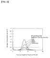
- FIG. 4 is a diagram that describes the action of the present invention, by showing stepwise how the nitrogen concentration peak is formed. In the figure, in case (1) where only plasma oxynitridation is performed on the gate insulating film, a large peak is formed on the semiconductor substrate side, and a small peak is formed on the gate electrode side. Similarly, in case (2) where the gate insulting film is subjected to plasma processing to form a base oxidation film, and then subjected to plasma oxynitridation, a large peak is formed on the semiconductor substrate side, and a small peak is formed on the gate electrode side. On the other hand, in case (3) where plasma nitridation processing is performed in addition to the steps in case (2), the nitrogen peak on the gate electrode side can be controlled.
- FIG. 5 (A), (B) are schematic illustrations showing substrate injection stress (write operation) and gate injection stress (erase operation). FIG. 6 is a graph showing the relationship (trap characteristics) between the injection charge and the gate voltage fluctuation during a write operation (substrate injection stress). FIG. 7 is a graph showing the relationship (SILC characteristics) between the injection charge and the leakage current during a write operation (substrate injection stress). FIG. 8 is a graph showing the relationship (SILC characteristics) between the injection charge and the leakage current during an erase operation (gate injection stress).
- [Evaluation of electrical characteristics using a capacitor (MOS-CAP)] (see FIG. 6 through FIG. 8)
- (1) Trap characteristics: From FIG. 6, it is apparent that an oxynitriding species (NH3) that contains hydrogen increases the number of electron traps and is therefore unsuitable. Electron traps cause a deterioration of the write/erase characteristics of flash memory. On the other hand, it is apparent that introducing NO gas reduces the number of electron traps, and diluting the NO gas yields further improvement.
-
- (2) SILC characteristics: SILC (Stress Introduced Leakage Current) is an electrical characteristic that reflects the data retention characteristics of the flash memory. When the leakage current is large, a greater amount of stored charge is leaked, causing deterioration in memory characteristics. Introducing NO gas reduces leakage current, but as shown in FIG. 7 and FIG. 8, diluting the NO gas yields further improvements to leakage current in both stress directions. Moreover, performing oxynitridation processing with a gas containing hydrogen produces nitric acid (HNO3), which can corrode the device.
- In a semiconductor storage device, such as flash memory or EEPROM, which operates by transferring a charge through an insulating film, electrical stress generated by the charge transfer is applied to the insulating film from both the substrate side and surface side. For this reason, the insulating film, which has nitrogen peaks at both interfaces, suppresses SILC (Stress-Induced Leakage Current) generation (see FIG. 7 and FIG. 8), thereby improving the characteristics of the semiconductor storage element.
- According to the present invention, nitrogen peaks can be formed simultaneously on the surface and interface sides of the gate insulating film of the semiconductor storage device (flash memory) (see FIG. 4). In this case, the use of an oxynitriding species (a gas for oxynitriding species) previously diluted by plasma excitation gas is preferred. If the concentration of the nitrogen peaks formed at each interface of the gate insulating film is 0.5 atomic% or less, excellent electrical characteristics can be obtained. Furthermore, it was confirmed that by performing plasma processing in the absence of hydrogen, electron capture characteristics are improved, and the write/erase characteristics of flash memory are also improved.
- FIG. 9 shows a configuration example of a plasma processing system for implementing the present invention. A
plasma processing system 10 has aprocessing vessel 11 which comprises asubstrate holder 12 that holds a silicon wafer W serving as the substrate to be processed. Gas inside theprocessing vessel 11 is discharged from anexhaust port 11B through an exhaust pump not shown in the figure. - An opening is formed in the device above the
processing vessel 11 at a position corresponding to the silicon wafer W placed on thesubstrate holder 12. This opening is covered by adielectric plate 13 made of quartz and substances such as A1203, A1N, and Si3N4. A planar antenna, here a RLSA (radial line slot antenna) 16, is positioned on top of the dielectric plate 13 (on the outside of the processing vessel 11). In thisantenna 16, a plurality of slots are formed through which electromagnetic waves are supplied from a waveguide can pass. The waveguide is disposed above (on the outside of) theantenna 16. - In the internal wall of the
processing vessel 11, a gas supply port 11A is provided for introducing gas during plasma processing. From this gas supply port 11A, gas pre-mixed in agas supply source 24 is introduced into theprocessing vessel 11. Though not shown in the figure, the flow rate of the gas can be controlled by using a flow regulating valve or the like at the mixing stage. - The
plasma processing system 10 used in the present invention comprises a microwave supply source 20 (electromagnetic wave generator) which, to excite the plasma, generates electromagnetic waves at several gigahertz, for example 2.45 GHz. The microwaves generated by themicrowave supply source 20 propagate through the waveguide and are introduced uniformly into theprocessing vessel 11 through theantenna 16. - The
microwave supply source 20 and thegas supply source 24 are controlled by a controller 27. Specifically, in thegas supply source 24, the mixing ratio and absolute flow rate of the NO gas contained in the oxynitriding species (gas of oxynitriding species) is adjusted according to the settings described earlier. For example, thegas supply source 24 operates such that the ratio (O:NO) of oxygen gas to NO gas is within a range from 1:0.000003 to 1:0.003. Alternatively, thegas supply source 24 operates such that the absolute flow rate of the NO gas contained in the oxynitriding species (gas of oxynitriding species) is within a range from 0.0001 to 0.01 (sccm). In another alternative, thegas supply source 24 operates such that the oxynitriding species contains 0.00001 to 0.01% NO gas relative to the total volume of gas introduced into theplasma processing vessel 11. - Control of the NO gas mixing ratio or absolute flow rate in the
gas supply source 24 can be implemented by a program (settings) stored in thecontroller 22. Moreover, control programs related to gas flow rates and mixing ratios can be stored on a storage device external to thecontroller 22. For example, the relevant program (settings) can be stored in advance on a recording medium such as CD-ROM, DVD, MO, floppy disk, HD, or memory, and either installed from that medium or loaded directly from the medium. There are no restrictions on the method used to record the program, and any optical, magnetic, opto-magnetic or other method can be used. - While preferred embodiments of the invention have been described above, the invention is not to be considered as being limited by the foregoing description, and is only limited by the scope of the appended claims.
-
- FIG. 1 is an explanatory diagram showing write and erase operations in a semiconductor storage device (flash memory), representing an application of the present invention.
- FIG. 2 is a graph showing the relationship in the gate insulating film, between the NO gas mixing ratio and the nitrogen concentration of the interface with the oxynitride film.
- FIG. 3 is a graph showing the variation in nitrogen concentration for different ratios of NO gas to the total volume of gas.
- FIG. 4 is a diagram that describes the action of the present invention, by showing stepwise how the nitrogen concentration peak is formed.
- FIG. 5 (A), (B) are schematic illustrations of substrate injection stress (write operation) and gate injection stress (erase operation).
- FIG. 6 is a graph showing the relationship (trap characteristics) between the injection charge and the gate voltage fluctuation during a write operation (substrate injection stress).
- FIG. 7 is a graph showing the relationship (SILC characteristics) between the injection charge and the leakage current during a write operation (substrate injection stress).
- FIG. 8 is a graph showing the relationship (SILC characteristics) between the injection charge and the leakage current during an erase operation (gate injection stress).
- FIG. 9 is an explanatory diagram (combined cross-sectional and block diagram) showing a configuration of a plasma processing system for implementing the present invention.
Claims (40)
- A method for fabricating a semiconductor storage device that operates by transferring a charge through a gate insulating film formed between a semiconductor substrate and a gate electrode, which is characterized by comprising:a step of introducing an oxynitriding species previously diluted by plasma excitation gas, into a plasma processing apparatus, generating an oxynitriding species by means of a plasma, and forming an oxynitride film on said semiconductor substrate as said gate insulating film,wherein said oxynitriding species contains NO gas at a ratio of 0.00001 to 0.01% to the total volume of gas introduced into said plasma processing apparatus.
- A fabricating method according to claim 1, wherein
said gate insulating film has nitrogen peaks of 0.02 to 0.5 atomic% at a first interface with said semiconductor substrate, and a second interface with said gate electrode. - A fabricating method according to either one of claims 1 and 2, wherein
said oxynitriding species contains NO gas at a ratio of 0.00001 to 0.01% to the total volume of gas introduced into said plasma processing apparatus. - A fabricating method according to claim 1, further comprising:a step for forming an oxide film on said semiconductor substrate prior to forming said oxynitride film.
- A fabricating method according to either one of claims 1 and 4, further comprising:a step for performing plasma nitridation processing on said gate insulating film, after forming said oxynitride film.
- A method for fabricating a semiconductor storage device that operates by transferring a charge through a gate insulating film formed between a semiconductor substrate and a gate electrode, which is
characterized by comprising:a step of introducing an oxynitriding species previously diluted by plasma excitation gas, into a plasma processing apparatus, generating an oxynitriding species by means of a plasma, and forming an oxynitride film on said semiconductor substrate as said gate insulating film,wherein a ratio of oxygen gas to NO gas (O:NO) in said oxynitriding species is within a range from 1:0.000003 to 1:0.003. - A method according to claim 6, wherein said gate insulating film has nitrogen peaks of 0.02 to 0.5 atomic% at a first interface with said semiconductor substrate, and a second interface with said gate electrode.
- A fabricating method according to either one of claims 6 and 7, further comprising a step for forming an oxide film on said semiconductor substrate prior to forming said oxynitride film.
- A fabricating method according to either one of claims 6 and 8, further comprising a step for performing plasma nitridation processing on said gate insulating film, after forming said oxynitride film.
- A method for fabricating a semiconductor storage device that operates by transferring a charge through a gate insulating film formed between a semiconductor substrate and a gate electrode, which is characterized by comprising:a step of introducing an oxynitriding species previously diluted by plasma excitation gas, into a plasma processing apparatus, generating an oxynitriding species by means of a plasma, and forming an oxynitride film on said semiconductor substrate as said gate insulating film,wherein an absolute flow rate of the NO gas in said oxynitriding species is within a range from 0.0001 to 0.01 (sccm).
- A fabricating method according to claim 10, wherein said gate insulating film has nitrogen peaks of 0.02 to 0.5 atomic% at a first interface with said semiconductor substrate, and a second interface with said gate electrode.
- A fabricating method according to claim 10, further comprising a step for forming an oxide film on said semiconductor substrate prior to forming said oxynitride film.
- A fabricating method according to either one of claims 10 and 12, further comprising a step for performing plasma nitridation processing on said gate insulating film, after forming said oxynitride film.
- A semiconductor storage device comprising a semiconductor substrate, a gate electrode formed on said semiconductor substrate, and a gate insulating film formed between said semiconductor substrate and the gate electrode,
wherein said gate insulating film has nitrogen peaks of 0.02 to 0.5 atomic% at a first interface with said semiconductor substrate and a second interface with said gate electrode. - A system for manufacturing a semiconductor storage device that operates by transferring a charge through a gate insulating film formed between a semiconductor substrate and a gate electrode, which is characterized by comprising:a plasma processing apparatus which performs plasma processing on a semiconductor wafer on which said semiconductor storage device is formed;a gas supply device which introduces the gas used in the plasma processing into said plasma processing apparatus; anda controller which controls at least a gas mixing ratio in said gas supply device,wherein the construction is such that under the control of said controller, said gas supply device introduces an oxynitriding species previously diluted by plasma excitation gas, into said plasma processing apparatus, thereby forming an oxynitride film on said semiconductor substrate as said gate insulating film,and under the control of said controller, said gas supply device operates in such a manner that said oxynitriding species contains NO gas at a ratio of 0.00001 to 0.01% to the total volume of gas introduced into said plasma processing apparatus.
- A system according to claim 15, wherein said controller controls so that said gate insulating film has nitrogen peaks of 0.02 to 0.5 atomic% at a first interface with said semiconductor substrate, and a second interface with said gate electrode.
- A system according to either one of claims 15 and 16, wherein said controller controls so that said oxynitriding species contains NO gas at a ratio of 0.00001 to 0.01% to the total volume of gas introduced into said plasma processing apparatus.
- A system according to any one of claims 15, 16 and 17, wherein said controller controls so as to form an oxide film on said semiconductor substrate prior to forming said oxynitride film.
- A system according to any one of claims 15, 16, 17 and 18, wherein
said controller controls so as to perform plasma nitridation processing on said gate insulating film, after forming said oxynitride film. - A recording medium storing a method used to fabricate a semiconductor storage device that operates by transferring a charge through a gate insulating film formed between a semiconductor substrate and a gate electrode, on which is recorded:a setting for introducing an oxynitriding species previously diluted by plasma excitation gas, into said plasma processing apparatus to form an oxynitride film on said semiconductor substrate as said gate insulating film; anda condition setting for ensuring that said oxynitriding species contains NO gas at a ratio of 0.00001 to 0.01% to the total volume of gas introduced into said plasma processing apparatus.
- A recording medium according to claim 20, recorded with a condition setting such that said gate insulating film has nitrogen peaks of 0.02 to 0.5 atomic% at a first interface with said semiconductor substrate, and a second interface with said gate electrode.
- A recording medium according to either one of claims 20 and 21, recorded with a condition setting such that said oxynitriding species contains NO gas at a ratio of 0.00001 to 0.01% to the total volume of gas introduced into said plasma processing apparatus.
- A recording medium according to any one of claims 20, 21 and 22, recorded with a setting for forming an oxide film on said semiconductor substrate prior to forming said oxynitride film.
- A recording medium according to any one of claims 20, 21, 22 and 23, recorded with a setting for performing plasma nitridation processing on said gate insulating film, after forming said oxynitride film.
- A system for manufacturing a semiconductor storage device that operates by transferring a charge through a gate insulating film formed between a semiconductor substrate and a gate electrode, which is
characterized by comprising:a plasma processing apparatus which performs plasma processing on a semiconductor wafer on which said semiconductor storage device is formed;a gas supply device which introduces the gas used in the plasma processing into said plasma processing apparatus; anda controller which controls at least a gas mixing ratio in said gas supply device,wherein the construction is such that under the control of said controller, said gas supply device introduces an oxynitriding species previously diluted by plasma excitation gas, into said plasma processing apparatus, thereby forming an oxynitride film on said semiconductor substrate as said gate insulating film,and under the control of said controller, said gas supply device operates in such a manner that a ratio of oxygen gas to NO gas (O:NO) in said oxynitriding species is within a range from 1:0.000003 to 1:0.003. - A system according to claim 25, wherein said controller controls so that said gate insulating film has nitrogen peaks of 0.02 to 0.5 atomic% at a first interface with said semiconductor substrate, and a second interface with said gate electrode.
- A system according to either one of claim 25 and claim 26, wherein said controller controls so as to form an oxide film on said semiconductor substrate prior to forming said oxynitride film.
- A system according to any one of claims 25, 26 and 27, wherein said controller controls so as to perform plasma nitridation processing on said gate insulating film, after forming said oxynitride film.
- A recording medium recorded with a method used to manufacture a semiconductor storage device that operates by transferring a charge through a gate insulating film formed between a semiconductor substrate and a gate electrode, on which is recorded:a setting for introducing an oxynitriding species previously diluted by plasma excitation gas, into said plasma processing apparatus to form an oxynitride film on said semiconductor substrate as said gate insulating film; anda condition setting for ensuring that a ratio of oxygen gas to NO gas (O:NO) in said oxynitriding species is within a range from 1:0.000003 to 1:0.003.
- A recording medium according to claim 29, recorded with a condition setting such that said gate insulating film has nitrogen peaks of 0.02 to 0.5 atomic% at a first interface with said semiconductor substrate, and a second interface with said gate electrode.
- A recording medium according to either one of claims 29 and 30, recorded with a setting for forming an oxide film on said semiconductor substrate prior to forming said oxynitride film.
- A recording medium according to any one of claims 29, 30 and 31, recorded with a setting for performing plasma nitridation processing on said gate insulating film, after forming said oxynitride film.
- A system for manufacturing a semiconductor storage device that operates by transferring a charge through a gate insulating film formed between a semiconductor substrate and a gate electrode, which is
characterized by comprising:a plasma processing apparatus which performs plasma processing on a semiconductor wafer on which said semiconductor storage device is formed;a gas supply device which introduces the gas used in the plasma processing into said plasma processing apparatus; anda controller which controls at least a gas mixing ratio in said gas supply device,wherein the construction is such that under the control of said controller, said gas supply device introduces an oxynitriding species previously diluted by plasma excitation gas, into said plasma processing apparatus, thereby forming an oxynitride film on said semiconductor substrate as said gate insulating film,and under the control of said controller, said gas supply device operates in such a manner that an absolute flow rate of the NO gas in said oxynitriding species is within a range from 0.0001 to 0.01 (sccm).. - A system according to claim 33, wherein said controller controls so that said gate insulating film has nitrogen peaks of 0.02 to 0.5 atomic% at a first interface with said semiconductor substrate, and a second interface with said gate electrode.
- A system according to either one of claims 33 and 34, wherein said controller controls so as to form an oxide film on said semiconductor substrate prior to forming said oxynitride film.
- A system according to any one of claims 33, 34 and 35, wherein said controller controls so as to perform plasma nitridation processing on said gate insulating film, after forming said oxynitride film.
- A recording medium recorded with a method used to manufacture a semiconductor storage device that operates by transferring a charge through a gate insulating film formed between a semiconductor substrate and a gate electrode, on which is recorded:a setting for introducing an oxynitriding species previously diluted by plasma excitation gas, into said plasma processing apparatus to form an oxynitride film on said semiconductor substrate as said gate insulating film; anda condition setting for ensuring that an absolute flow rate of the NO gas in said oxynitriding species is within a range from 0.0001 to 0.01 (sccm)..
- A recording medium according to claim 37, recorded with a condition setting such that said gate insulating film has nitrogen peaks of 0.02 to 0.5 atomic% at a first interface with said semiconductor substrate, and a second interface with said gate electrode.
- A recording medium according to either one of claims 37 and 38, recorded with a setting for forming an oxide film on said semiconductor substrate prior to forming said oxynitride film.
- A recording medium according to any one of claims 37, 38 and 39, recorded with a setting for performing plasma nitridation processing on said gate insulating film, after forming said oxynitride film.
Applications Claiming Priority (2)
| Application Number | Priority Date | Filing Date | Title |
|---|---|---|---|
| JP2004290768A JP4579637B2 (en) | 2004-10-01 | 2004-10-01 | Semiconductor memory device and manufacturing method thereof |
| PCT/JP2005/018179 WO2006038566A1 (en) | 2004-10-01 | 2005-09-30 | Semiconductor storage device and method for manufacturing the same |
Publications (2)
| Publication Number | Publication Date |
|---|---|
| EP1811562A1 true EP1811562A1 (en) | 2007-07-25 |
| EP1811562A4 EP1811562A4 (en) | 2008-11-19 |
Family
ID=36142640
Family Applications (1)
| Application Number | Title | Priority Date | Filing Date |
|---|---|---|---|
| EP05787588A Ceased EP1811562A4 (en) | 2004-10-01 | 2005-09-30 | SEMICONDUCTOR STORAGE DEVICE AND METHOD FOR MANUFACTURING THE SAME |
Country Status (7)
| Country | Link |
|---|---|
| US (1) | US8067809B2 (en) |
| EP (1) | EP1811562A4 (en) |
| JP (1) | JP4579637B2 (en) |
| KR (1) | KR100923715B1 (en) |
| CN (1) | CN100559567C (en) |
| TW (1) | TWI397153B (en) |
| WO (1) | WO2006038566A1 (en) |
Cited By (1)
| Publication number | Priority date | Publication date | Assignee | Title |
|---|---|---|---|---|
| US7855153B2 (en) | 2008-02-08 | 2010-12-21 | Semiconductor Energy Laboratory Co., Ltd. | Method for manufacturing semiconductor device |
Families Citing this family (5)
| Publication number | Priority date | Publication date | Assignee | Title |
|---|---|---|---|---|
| JP5232425B2 (en) * | 2007-09-10 | 2013-07-10 | ルネサスエレクトロニクス株式会社 | Nonvolatile semiconductor memory device and manufacturing method thereof |
| CN102263021B (en) * | 2010-05-28 | 2013-06-19 | 中芯国际集成电路制造(上海)有限公司 | Method for preparing low voltage gate oxide |
| JP5931611B2 (en) * | 2012-07-03 | 2016-06-08 | ルネサスエレクトロニクス株式会社 | Manufacturing method of semiconductor device |
| JP6086933B2 (en) * | 2015-01-06 | 2017-03-01 | 株式会社日立国際電気 | Semiconductor device manufacturing method, substrate processing apparatus, and program |
| WO2017119424A1 (en) * | 2016-01-08 | 2017-07-13 | 日本ゼオン株式会社 | Nitrile rubber composition, crosslinkable nitrile rubber composition and crosslinked rubber article |
Family Cites Families (21)
| Publication number | Priority date | Publication date | Assignee | Title |
|---|---|---|---|---|
| JP3133480B2 (en) | 1992-04-15 | 2001-02-05 | 昭和シェル石油株式会社 | Method for producing optically active halogen-containing alcohol |
| JP3288796B2 (en) * | 1993-03-15 | 2002-06-04 | 株式会社東芝 | Semiconductor device |
| US5464792A (en) * | 1993-06-07 | 1995-11-07 | Motorola, Inc. | Process to incorporate nitrogen at an interface of a dielectric layer in a semiconductor device |
| JP3072000B2 (en) * | 1994-06-23 | 2000-07-31 | 株式会社半導体エネルギー研究所 | Method for manufacturing semiconductor device |
| JP3600326B2 (en) * | 1994-09-29 | 2004-12-15 | 旺宏電子股▲ふん▼有限公司 | Nonvolatile semiconductor memory device and manufacturing method thereof |
| JP3222404B2 (en) * | 1997-06-20 | 2001-10-29 | 科学技術振興事業団 | Method and apparatus for forming insulating film on semiconductor substrate surface |
| US6559007B1 (en) | 2000-04-06 | 2003-05-06 | Micron Technology, Inc. | Method for forming flash memory device having a tunnel dielectric comprising nitrided oxide |
| JP5068402B2 (en) * | 2000-12-28 | 2012-11-07 | 公益財団法人国際科学振興財団 | Dielectric film and method for forming the same, semiconductor device, nonvolatile semiconductor memory device, and method for manufacturing semiconductor device |
| US6773999B2 (en) * | 2001-07-18 | 2004-08-10 | Matsushita Electric Industrial Co., Ltd. | Method for treating thick and thin gate insulating film with nitrogen plasma |
| JP2003060198A (en) | 2001-08-10 | 2003-02-28 | Matsushita Electric Ind Co Ltd | Semiconductor device and manufacturing method thereof |
| US6548422B1 (en) | 2001-09-27 | 2003-04-15 | Agere Systems, Inc. | Method and structure for oxide/silicon nitride interface substructure improvements |
| US6960537B2 (en) | 2001-10-02 | 2005-11-01 | Asm America, Inc. | Incorporation of nitrogen into high k dielectric film |
| SG152910A1 (en) * | 2001-12-07 | 2009-06-29 | Tokyo Electron Ltd | Nitriding method for insulation film, semiconductor device and production method for semiconductor device, substrate treating device and substrate treating method |
| US6555485B1 (en) * | 2002-01-28 | 2003-04-29 | United Microelectronics Corp. | Method for fabricating a gate dielectric layer |
| KR20030077436A (en) * | 2002-03-26 | 2003-10-01 | 가부시키가이샤 히다치 고쿠사이 덴키 | Method for manufacturing a semiconductor device and apparatus for manufacturing a semiconductor |
| TWI225668B (en) * | 2002-05-13 | 2004-12-21 | Tokyo Electron Ltd | Substrate processing method |
| US6716705B1 (en) * | 2002-06-03 | 2004-04-06 | Lattice Semiconductor Corporation | EEPROM device having a retrograde program junction region and process for fabricating the device |
| DE10239429A1 (en) | 2002-08-28 | 2004-03-11 | Robert Bosch Gmbh | Fuel injection device for an internal combustion engine |
| KR100470941B1 (en) | 2002-12-26 | 2005-03-10 | 주식회사 하이닉스반도체 | Method of forming oxynitride film |
| US6797650B1 (en) * | 2003-01-14 | 2004-09-28 | Advanced Micro Devices, Inc. | Flash memory devices with oxynitride dielectric as the charge storage media |
| WO2004070816A1 (en) * | 2003-02-06 | 2004-08-19 | Tokyo Electron Limited | Plasma processing method, semiconductor substrate and plasma processing system |
-
2004
- 2004-10-01 JP JP2004290768A patent/JP4579637B2/en not_active Expired - Fee Related
-
2005
- 2005-09-30 TW TW094134323A patent/TWI397153B/en not_active IP Right Cessation
- 2005-09-30 KR KR1020077002546A patent/KR100923715B1/en not_active Expired - Fee Related
- 2005-09-30 US US11/576,499 patent/US8067809B2/en not_active Expired - Fee Related
- 2005-09-30 CN CNB2005800333121A patent/CN100559567C/en not_active Expired - Fee Related
- 2005-09-30 EP EP05787588A patent/EP1811562A4/en not_active Ceased
- 2005-09-30 WO PCT/JP2005/018179 patent/WO2006038566A1/en not_active Ceased
Cited By (2)
| Publication number | Priority date | Publication date | Assignee | Title |
|---|---|---|---|---|
| US7855153B2 (en) | 2008-02-08 | 2010-12-21 | Semiconductor Energy Laboratory Co., Ltd. | Method for manufacturing semiconductor device |
| US8324699B2 (en) | 2008-02-08 | 2012-12-04 | Semiconductor Energy Laboratory Co., Ltd. | Method for manufacturing semiconductor device |
Also Published As
| Publication number | Publication date |
|---|---|
| TWI397153B (en) | 2013-05-21 |
| CN101032020A (en) | 2007-09-05 |
| KR100923715B1 (en) | 2009-10-27 |
| US8067809B2 (en) | 2011-11-29 |
| JP4579637B2 (en) | 2010-11-10 |
| US20090072327A1 (en) | 2009-03-19 |
| TW200629483A (en) | 2006-08-16 |
| JP2006324264A (en) | 2006-11-30 |
| WO2006038566A1 (en) | 2006-04-13 |
| EP1811562A4 (en) | 2008-11-19 |
| KR20070088468A (en) | 2007-08-29 |
| CN100559567C (en) | 2009-11-11 |
Similar Documents
| Publication | Publication Date | Title |
|---|---|---|
| JP5706946B2 (en) | Plasma etching method and plasma etching apparatus | |
| CN100429753C (en) | Plasma processing method, semiconductor substrate, and plasma processing apparatus | |
| US20180076063A1 (en) | Substrate processing apparatus | |
| US10128258B2 (en) | Oxide formation in a plasma process | |
| EP1900001A2 (en) | Methods and apparatus for incorporating nitrogen in oxide films | |
| US8067809B2 (en) | Semiconductor storage device including a gate insulating film with a favorable nitrogen concentration profile and method for manufacturing the same | |
| CN108834429B (en) | Method for manufacturing semiconductor device, recording medium, and substrate processing apparatus | |
| CN100587922C (en) | Method for forming silicon oxide film and method for manufacturing semiconductor device | |
| US7205217B2 (en) | Method for forming trench gate dielectric layer | |
| US20060024864A1 (en) | Substrate processing method | |
| KR101153310B1 (en) | Method for manufacturing a mos semiconductor memory device, and plasma cvd device | |
| US7858509B2 (en) | High-dielectric film substrate processing method | |
| CN101120437B (en) | Dielectric film and method for forming same | |
| JP2008187180A (en) | Manufacturing method of flash memory | |
| JP2011165743A (en) | Method of manufacturing semiconductor-device | |
| CN122028432A (en) | Preparation method of ONO structure of nonvolatile memory with low chlorine content | |
| CN100433271C (en) | Method for manufacturing inter-polysilicon dielectric layer | |
| CN121152210A (en) | Methods to improve thin film stability in semiconductor devices | |
| CN120786893A (en) | Method for forming semiconductor structure | |
| WO2003073492A1 (en) | Method for processing substrate | |
| CN120199684A (en) | A kind of ONO structure and its preparation method and application | |
| KR20090010604A (en) | Manufacturing method of nonvolatile memory device |
Legal Events
| Date | Code | Title | Description |
|---|---|---|---|
| PUAI | Public reference made under article 153(3) epc to a published international application that has entered the european phase |
Free format text: ORIGINAL CODE: 0009012 |
|
| 17P | Request for examination filed |
Effective date: 20070425 |
|
| AK | Designated contracting states |
Kind code of ref document: A1 Designated state(s): BE DE FR IT NL |
|
| DAX | Request for extension of the european patent (deleted) | ||
| RBV | Designated contracting states (corrected) |
Designated state(s): BE DE FR IT NL |
|
| A4 | Supplementary search report drawn up and despatched |
Effective date: 20081020 |
|
| RIC1 | Information provided on ipc code assigned before grant |
Ipc: H01L 21/8247 20060101AFI20060929BHEP Ipc: H01L 27/115 20060101ALI20081014BHEP Ipc: H01L 29/792 20060101ALI20081014BHEP Ipc: H01L 29/51 20060101ALI20081014BHEP Ipc: H01L 29/788 20060101ALI20081014BHEP Ipc: H01L 21/318 20060101ALI20081014BHEP |
|
| 17Q | First examination report despatched |
Effective date: 20090126 |
|
| REG | Reference to a national code |
Ref country code: DE Ref legal event code: R003 |
|
| STAA | Information on the status of an ep patent application or granted ep patent |
Free format text: STATUS: THE APPLICATION HAS BEEN REFUSED |
|
| 18R | Application refused |
Effective date: 20140427 |