EP1808912A2 - Electron transport compound and organic light emitting device comprising the same - Google Patents
Electron transport compound and organic light emitting device comprising the same Download PDFInfo
- Publication number
- EP1808912A2 EP1808912A2 EP07000776A EP07000776A EP1808912A2 EP 1808912 A2 EP1808912 A2 EP 1808912A2 EP 07000776 A EP07000776 A EP 07000776A EP 07000776 A EP07000776 A EP 07000776A EP 1808912 A2 EP1808912 A2 EP 1808912A2
- Authority
- EP
- European Patent Office
- Prior art keywords
- light emitting
- layer
- electron
- substituted
- organic light
- Prior art date
- Legal status (The legal status is an assumption and is not a legal conclusion. Google has not performed a legal analysis and makes no representation as to the accuracy of the status listed.)
- Granted
Links
Classifications
-
- H—ELECTRICITY
- H10—SEMICONDUCTOR DEVICES; ELECTRIC SOLID-STATE DEVICES NOT OTHERWISE PROVIDED FOR
- H10K—ORGANIC ELECTRIC SOLID-STATE DEVICES
- H10K85/00—Organic materials used in the body or electrodes of devices covered by this subclass
- H10K85/60—Organic compounds having low molecular weight
- H10K85/615—Polycyclic condensed aromatic hydrocarbons, e.g. anthracene
- H10K85/622—Polycyclic condensed aromatic hydrocarbons, e.g. anthracene containing four rings, e.g. pyrene
-
- H—ELECTRICITY
- H10—SEMICONDUCTOR DEVICES; ELECTRIC SOLID-STATE DEVICES NOT OTHERWISE PROVIDED FOR
- H10K—ORGANIC ELECTRIC SOLID-STATE DEVICES
- H10K85/00—Organic materials used in the body or electrodes of devices covered by this subclass
- H10K85/60—Organic compounds having low molecular weight
- H10K85/649—Aromatic compounds comprising a hetero atom
- H10K85/654—Aromatic compounds comprising a hetero atom comprising only nitrogen as heteroatom
-
- H—ELECTRICITY
- H10—SEMICONDUCTOR DEVICES; ELECTRIC SOLID-STATE DEVICES NOT OTHERWISE PROVIDED FOR
- H10K—ORGANIC ELECTRIC SOLID-STATE DEVICES
- H10K50/00—Organic light-emitting devices
- H10K50/10—OLEDs or polymer light-emitting diodes [PLED]
- H10K50/14—Carrier transporting layers
-
- H—ELECTRICITY
- H10—SEMICONDUCTOR DEVICES; ELECTRIC SOLID-STATE DEVICES NOT OTHERWISE PROVIDED FOR
- H10K—ORGANIC ELECTRIC SOLID-STATE DEVICES
- H10K85/00—Organic materials used in the body or electrodes of devices covered by this subclass
- H10K85/30—Coordination compounds
- H10K85/321—Metal complexes comprising a group IIIA element, e.g. Tris (8-hydroxyquinoline) gallium [Gaq3]
- H10K85/324—Metal complexes comprising a group IIIA element, e.g. Tris (8-hydroxyquinoline) gallium [Gaq3] comprising aluminium, e.g. Alq3
-
- Y—GENERAL TAGGING OF NEW TECHNOLOGICAL DEVELOPMENTS; GENERAL TAGGING OF CROSS-SECTIONAL TECHNOLOGIES SPANNING OVER SEVERAL SECTIONS OF THE IPC; TECHNICAL SUBJECTS COVERED BY FORMER USPC CROSS-REFERENCE ART COLLECTIONS [XRACs] AND DIGESTS
- Y10—TECHNICAL SUBJECTS COVERED BY FORMER USPC
- Y10S—TECHNICAL SUBJECTS COVERED BY FORMER USPC CROSS-REFERENCE ART COLLECTIONS [XRACs] AND DIGESTS
- Y10S428/00—Stock material or miscellaneous articles
- Y10S428/917—Electroluminescent
Definitions
- This document relates to an electron transport compound and an organic light emitting device comprising the same.
- an organic light emitting display is a self-emitting display for emitting light by electrically exciting a fluorescent compound and has been spotlighted as a future generation display that can solve problems of a liquid crystal display as it can be driven in a low voltage, easily reduce a thickness, have a wide viewing angle and a fast response speed, etc.
- the organic light emitting device comprises an organic emitting layer between an anode and a cathode.
- the organic light emitting device forms an exciton, which is a hole-electron pair, by coupling a hole received from the anode and an electron received from the cathode within the organic light emitting layer and emits light by generating energy when the exciton returns to a ground level.
- the organic light emitting device further comprises a hole(electron) injecting layer and/or a hole(electron) transporting layer between the anode or the cathode and the emitting layer.
- a process of manufacturing organic light emitting device is as follows.
- an anode is formed on a transparent substrate.
- ITO Indium Tin Oxide
- HIL hole injecting layer
- CuPc copper phthalocyanine
- HTL hole transport layer
- NPB 4,4'-bis[N-(1-naphthyl)-N-phenthylamino]-biphenyl
- the organic emitting layer may comprise a host and a dopant.
- a host and a dopant.
- tris(8-hydroxy-quinolatealuminum (Alq 3 ) as the host is deposited in a thickness of about 30 to 60nm and as a dopant, N-Methylquinacridone (MQD) is doped in the host.
- Alq 3 tris(8-hydroxy-quinolatealuminum
- MQD N-Methylquinacridone
- An electron transport layer (ETL) and an electron injecting layer (EIL) are consecutively formed or one electron injecting and transport layer is formed on the organic emitting layer.
- ETL electron transport layer
- EIL electron injecting layer
- an electron transport compound for an electron injecting layer or an electron transport layer has problems of low electron transport efficiency in using for a display device and difficulty of deposition. Further, a conventional electron transport compound has a problem of a short lifetime due to high possibility of crystallization and deterioration.
- An object of this document is to provide an organic light emitting device having a pyrene based electron transport compound and an electron injecting and transport layer comprising the electron transport compound.
- Another object of this document is to provide an electron transport compound that has high electron transport efficiency, and good deposition characteristics, prevents crystallization, and has no influence on a lifetime of organic light emitting device.
- Another object of this document is to provide an organic light emitting device having high brightness, high efficiency, and a long lifetime using an electron transport compound.
- this document provides a pyrene based electron transport compound having chemical formula 1.
- Pyrene based compound of chemical formula 1-1 is a very important compound among hydrocarbons.
- carbons are numbered clockwise starting with a carbon having a substituent A-C.
- an electron transport compound according to an embodiment of this document comprises a pyrene based compound in which A-C is bonded to carbon 1 and 6, and B is bonded to carbon 3 and 8.
- the substituents A, B, and C may be substituted or not substituted.
- the electron transport compound is a compound that injects an electron from a cathode to other layer or transports an injected electron to other layers.
- an electron transport compound is a compound that may be a material of an electron injecting layer, an electron transport layer, or an electron injecting and transport layer in which the electron injecting layer and the electron transport layer are mixed.
- the electron injecting and transport layer is used to generally designate layers, which are related to injecting and transporting of an electron, such as an electron injecting layer, an electron transport layer, or an electron injecting and transport layer in which the electron injecting layer and the electron transport layer are mixed.
- a that is substituted or is not substituted may be selected from a group consisting of pyridinyl, quinolinyl, isoquinolinyl, quinoxalinyl, bipyridinyl, terpyridinyl, and phenanthrolinyl.
- B and C that are substituted or are not substituted may be selected from a group consisting of phenyl, biphenyl, naphthyl, fluorenyl, terphenyl, phenanthrolinyl, phenanthryl, and anthryl.
- a substituent of the A, B, and C may be selected from a group consisting of aryl, alkyl, aryloxy, alkoxy, allylamino, alkylamino, halogen, and cyano.
- a substituent of the A, B, and C may be selected from a group consisting of phenyl, biphenyl, triphenylmethyl, phenylethylidene, diphenylethylidene, phenylmethylidyne, phenoxy, tolyoxy, methyl, ethyl, propyl, i-propyl, t-butyl, cyclohexyl, diphenylamino, morpholine, methoxy, ethoxy, propoxy, butoxy, dimethylamino, diphenylamino, fluorine, and chlorine.
- R1, R2, R3, R4, R5, and R6 is CH3, and the remaining ones are H.
- electron transport compounds can be formed by combining the pyrene based electron transport compound of chemical formula 1-1 with substituents of chemical formulas 1-2 to 1-4.
- the electron transport compounds can be easily selected by those skilled in the art according to necessity of brightness, color purity, or a driving voltage.
- the electron injecting and transport layer may be one or both of an electron injecting layer or an electron transport layer.
- the electron injecting and transport layer may be formed between an organic light emitting layer and a cathode.
- the electron injecting and transport layer may have a different layer position when participating in injecting and transporting of an electron as described above.
- 1,5-di(4-(3'-pyridine)phenyl)-3,6-diphenylpyrene among electron transport compounds of an electron injecting and transport layer of organic light emitting device according to a first embodiment of this document is synthesized as follows.
- reaction mixture was extracted using dichloromethane and water and distilled under a reduced pressure, then the distilled mixture was purified by passing through a silica gel column. The purified mixture was distilled under a reduced pressure again. The purified and distilled mixture was recrystallized using dichloromethane and methanol and filtered. Then 1,5-di(4-(3'-pyridine)-phenyl)pyrene was obtained.
- 1,5-di(4-(3'-pyridine)-phenyl)pyrene was put in 80mL of acetic acid and they were stirred in a dried three neck round bottom flask. After 1.9g (0.0118mol) of bromine (Br 2 ) was added to the reaction mixture at a room temperature and when a reaction was ended, filtering was performed. By washing and then drying the reaction mixture with excessive distilled water, 3,6-dibromo-1,5-di(4-(3'-pyridine)-phenyl)pyrene was obtained.
- reaction mixture was extracted using dichloromethane and water and distilled under a reduced pressure.
- the distilled mixture was purified by passing through a silica gel column, then distilled under a reduced pressure again.
- the purified and distilled mixture was recrystallized using dichloromethane and methanol and filtered. Then, 1,5-di(4-(3'-pyridine)phenyl)-3,6-diphenylpyrene, which is a final product was obtained.
- organic light emitting device was manufactured using the electron transport compound synthesized in the synthesis example and conventional organic light emitting device was manufactured using a conventional material in the electron injecting and transport layer. Then brightness, color purity, and a driving voltage thereof were measured under the same condition.
- an organic light emitting device manufactured using other pyrene based electron transport compound of chemical formula 1-1 may show the same or similar result as examples. The result may be expected by those skilled in the art and thus descriptions of other compounds will be omitted.
- a comparative example Conventional organic light emitting device
- ITO glass was washed after being patterned so that a light emitting area thereof became 3mm X 3mm.
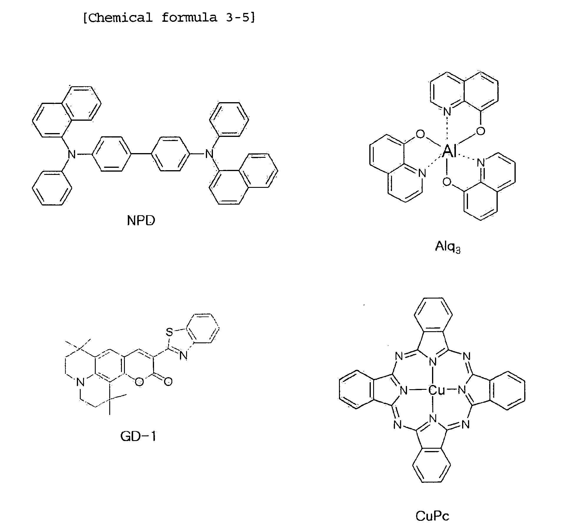
- a hole injecting layer/a hole transport layer/a green organic emitting layer (host+dopant)/an electron injecting and transport layer/cathode (CuPc (650 ⁇ ) /NPD(400 ⁇ ) /Alq 3 (200 ⁇ ) +GD-1(1%)(50 ⁇ )/Alq 3 (350 ⁇ )/LiF(5 ⁇ )/Al(1000 ⁇ )) were formed on ITO in 1.0X10 -6 torr.
- ITO glass was washed after being patterned so that a light emitting area thereof became 3mm X 3mm.
- a hole injecting layer/a hole transport layer/a green organic emitting layer (host+dopant)/an electron injecting and transport layer/cathode (CuPc(650 ⁇ ) /NPD(400 ⁇ ) /Alq 3 (200 ⁇ ) +GD-1 (1%) (50 ⁇ ) /PA-1(350 ⁇ )/LiF(5 ⁇ )/Al(1000 ⁇ )) were formed on ITO in 1.0X10 -6 torr.
- PA-1 is a pyrene based electron transport compound of chemical formula 1-6.
- ITO glass was washed after being patterned so that a light emitting area thereof became 3mm X 3mm.
- PA-2 is a pyrene based electron transport compound of chemical formula 1-7.
- ITO glass was washed after being patterned so that a light emitting area thereof became 3mm X 3mm.
- a hole injecting layer/a hole transport layer/a green organic emitting layer (host+dopant)/an electron injecting and transport layer/cathode (CuPc(650 ⁇ )/NPD(400 ⁇ )/Alq 3 (200 ⁇ )+GD-1(1%) (50 ⁇ )/PB-1(350 ⁇ )/LiF(5 ⁇ )/A1(1000 ⁇ )) were formed on ITO in 1.0X10 -6 torr.
- PB-1 is a pyrene based electron transport compound of chemical formula 1-8.
- ITO glass was washed after being patterned so that a light emitting area thereof became 3mm X 3mm.
- a hole injecting layer/a hole transport layer/a green organic emitting layer (host+dopant)/an electron injecting and transport layer/cathode (CuPc (650 ⁇ ) /NPD (400 ⁇ ) /Alq 3 (200 ⁇ ) +GD-1 (1%) (50 ⁇ ) /PC-1(350 ⁇ )/LiF(5 ⁇ )/Al(1000 ⁇ )) were formed on ITO in 1.0X10 -6 torr PC-1 is a pyrene based electron transport compound of chemical formula 1-9.
- ITO glass was washed after being patterned so that a light emitting area thereof became 3mm X 3mm.
- a hole injecting layer/a hole transport layer/a green organic emitting layer (host+dopant)/an electron injecting and transport layer/cathode (CuPc(650 ⁇ )/NPD(400 ⁇ )/Alq 3 (200 ⁇ ) +GD-1(1%) (50 ⁇ ) /PE-1(350 ⁇ )/LiF(5 ⁇ )/Al(1000 ⁇ )) were formed on ITO in 1.0X10 -6 torr.
- PE-1 is a pyrene based electron transport compound of chemical formula 1-10.
- Example 6 - Organic light emitting device according to a sixth embodiment of this document
- ITO glass was washed after being patterned so that a light emitting area thereof became 3mm X 3mm.
- a hole injecting layer/a hole transport layer/a green organic emitting layer (host+dopant)/an electron injecting and transport layer/cathode (CuPc(650 ⁇ ) /NPD(400 ⁇ ) /Alq 3 (200 ⁇ ) +GD-1 (1%) (50 ⁇ ) /PF-1(350 ⁇ )/LiF(5 ⁇ )/Al(1000 ⁇ )) were formed on ITO in 1.0X10 -6 torr.
- PF-1 is a pyrene based electron transport compound of chemical formula 1-11.
- Example 7 - Organic light emitting device according to a seventh embodiment of this document
- ITO glass was washed after being patterned so that a light emitting area thereof became 3mm X 3mm.
- a hole injecting layer/a hole transport layer/a green organic emitting layer (host+dopant)/an electron injecting and transport layer/cathode (CuPc (650 ⁇ ) /NPD(400 ⁇ ) /Alq 3 (200 ⁇ ) +GD-1 (1%) (50 ⁇ ) /PK-1(350 ⁇ )/LiF(5 ⁇ )/Al(1000 ⁇ )) were formed on ITO in 1.0X10 -6 torr.
- PK-1 is a pyrene based electron transport compound of chemical formula 1-12.
- organic light emitting device comprise pyrene based electron transport compound of chemical formula 1-1 described above in an electron injecting and transport layer
- brightness of organic light emitting device according to embodiments of this document improves by minimum 77.2% (the sixth embodiment) and maximum 26% (the seventh embodiment), compared to brightness of conventional organic light emitting device. It can be seen that a driving voltage of organic light emitting device according to embodiments of this document was decreased to 4.7V to 5.5V, compared to a driving voltage of conventional organic light emitting device.
- this document provides a pyrene based electron transport compound having chemical formula 2-1.
- Pyrene based compound of chemical formula 2-1 is a very important compound among hydrocarbons.
- carbons are numbered clockwise starting with a carbon having a substituent A-C.
- an electron transport compound according to an embodiment of this document comprises a pyrene based compound in which A-C is bonded to carbon 1 and B is bonded to carbon 3, 6 and 8.
- the substituents A, B, and C may be substituted or not substituted.
- the electron transport compound is a compound that injects an electron from a cathode to other layer or transports an injected electron to other layers.
- an electron transport compound is a compound that may be a material of an electron injecting layer, an electron transport layer, or an electron injecting and transport layer in which the electron injecting layer and the electron transport layer are mixed.
- the electron injecting and transport layer is used to generally designate layers, which are related to injecting and transporting of an electron, such as an electron injecting layer, an electron transport layer, or an electron injecting and transport layer in which the electron injecting layer and the electron transport layer are mixed.
- a that is substituted or is not substituted may be selected from a group consisting of pyridinyl, quinolinyl, isoquinolinyl, quinoxalinyl, bipyridinyl, terpyridinyl, and phenanthrolinyl.
- B and C that are substituted or are not substituted may be selected from a group consisting of phenyl, biphenyl, naphthyl, fluorenyl, terphenyl, phenanthrolinyl, phenanthryl, and anthryl.
- a substituent of the A, B, and C may be selected from a group consisting of aryl, alkyl, aryloxy, alkoxy, allylamino, alkylamino, halogen, and cyano.
- a substituent of the A, B, and C may be selected from a group consisting of phenyl, biphenyl, triphenylmethyl, phenylethylidene, diphenylethylidene, phenylmethylidyne, phenoxy, tolyoxy, methyl, ethyl, propyl, i-propyl, t-butyl, cyclohexyl, diphenylamino, morpholine, methoxy, ethoxy, propoxy, butoxy, dimethylamino, diphenylamino, fluorine, and chlorine.
- R1, R2, R3, R4, R5, and R6 is CH3, and the remaining ones are H.
- electron transport compounds can be formed by combining the pyrene based electron transport compound of chemical formula 2-1 with substituents of chemical formulas 2-2 to 2-4.
- the electron transport compounds can be easily selected from organic light emitting device such as organic light emitting device by those skilled in the art according to necessity of brightness, color purity, or a driving voltage.
- the electron injecting and transport layer may be one or both of an electron injecting layer or an electron transport layer.
- the electron injecting and transport layer may be formed between an organic or inorganic light emitting layer and a cathode.
- the electron injecting and transport layer may have a different layer position when participating in injecting and transporting of an electron as described above.
- reaction mixture was extracted using dichloromethane and water and distilled under a reduced pressure then the distilled mixture was purified by passing through a silica gel column. The purified mixture was distilled under a reduced pressure again. The purified and distilled mixture was recrystallized using dichloromethane and methanol and filtered. Then 1-(4-(3'-pyridine)-phenyl)pyrene was obtained.
- reaction mixture was extracted using dichloromethane and water and distilled under a reduced pressure then the distilled mixture was purified by passing through a silica gel column. The purified mixture was distilled under a reduced pressure again. The purified and distilled mixture was recrystallized using dichloromethane and methanol and filtered. Then 1-(4-(3'-pyridine)-phenyl)-3,6,8-triphenylenepyrene was obtained.
- organic light emitting device was manufactured using the electron transport compound synthesized in the synthesis example and conventional organic light emitting device was manufactured using a conventional material in the electron injecting and transport layer. Then brightness, color purity, and a driving voltage thereof were measured under the same condition.
- an organic light emitting device manufactured using other pyrene based electron transport compound of chemical formula 1-1 may show the same or similar result as examples. The result may be expected by those skilled in the art and thus descriptions of other compounds will be omitted.
- a comparative example Conventional organic light emitting device
- ITO glass was washed after being patterned so that a light emitting area thereof became 3mm X 3mm.
- a hole injecting layer/a hole transport layer/a green organic emitting layer (host+dopant)/an electron injecting and transport layer/cathode (CuPc(650 ⁇ ) /NPD(400 ⁇ ) /Alq 3 (200 ⁇ ) +GD-1(1%) (50 ⁇ )/Alq 3 (350 ⁇ )/LiF(5 ⁇ )/Al(1000 ⁇ )) were formed on ITO in 1.0X10 -6 torr.
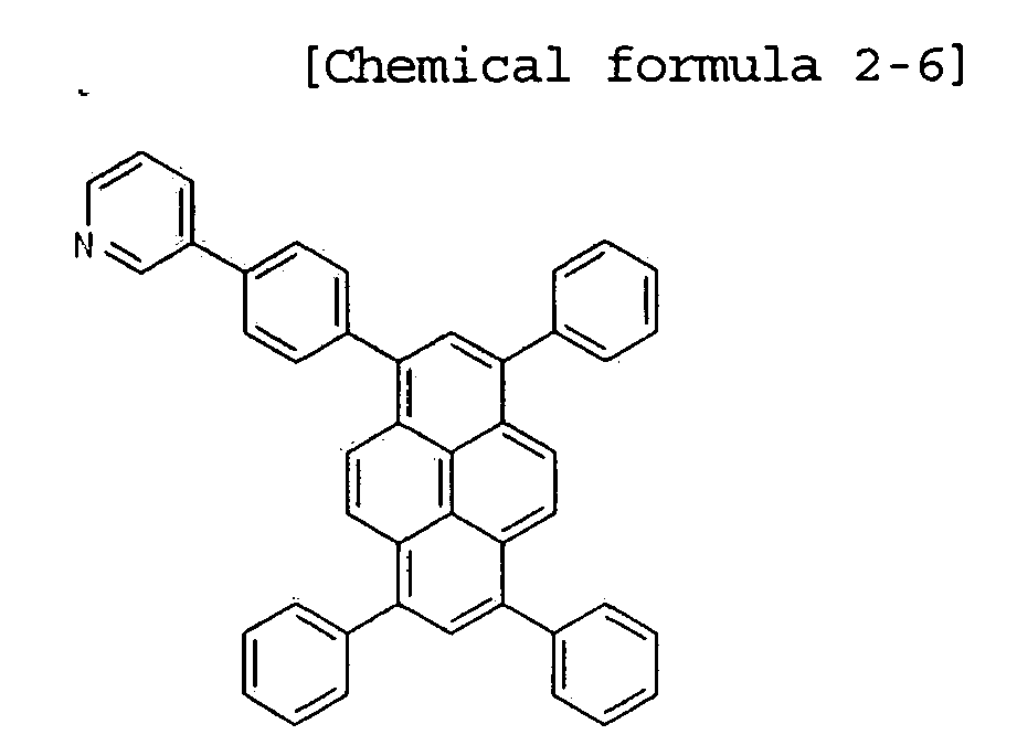
- TPA-1 is an electron transport compound of 1-(4-(3'-pyridine)phenyl)-3,6,8-trhenylpyrene of chemical formula 2-6 in which A is pyridine and B and C are phenyl.
- ITO glass was washed after being patterned so that a light emitting area thereof became 3mm X 3mm.
- a hole injecting layer/a hole transport layer/a green organic emitting layer (host+dopant)/an electron injecting and transport layer/cathode CuPc(650 ⁇ ) /NPD (400 ⁇ ) /Alq 3 (200 ⁇ ) +GD-1 (1%) (50 ⁇ ) /TPB-1(350 ⁇ )/LiF(5 ⁇ )/Al(1000 ⁇ )were formed on ITO in 1.0X10 -6 torr.
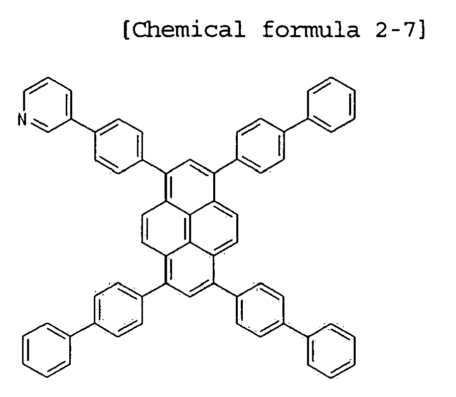
- TPB-8 is a pyrene based electron transport compound of chemical formula 2-7 in which A is pyridine, B is biphenyl and C is phenyl.
- ITO glass was washed after being patterned so that a light emitting area thereof became 3mm X 3mm.
- a hole injecting layer/a hole transport layer/a green organic emitting layer (host+dopant)/an electron injecting and transport layer/cathode (CuPc (650 ⁇ ) /NPD (400 ⁇ ) /Alq 3 (200 ⁇ ) +GD-1 (1%) (50 ⁇ ) /TPC-1(350 ⁇ )/LiF(5 ⁇ )/Al(1000 ⁇ )) were formed on ITO in 1.0X10 -6 torr.
- TPC-1 is a pyrene based electron transport compound of chemical formula 2-8.
- ITO glass was washed after being patterned so that a light emitting area thereof became 3mm X 3mm.
- a hole injecting layer/a hole transport layer/a green organic emitting layer (host+dopant)/an electron injecting and transport layer/cathode (CuPc (650 ⁇ ) /NPD (400 ⁇ ) /Alq 3 (200 ⁇ ) +GD-1 (1%) (50 ⁇ ) /TPE-1(350 ⁇ )/LiF(5 ⁇ )/Al(1000 ⁇ )) were formed on ITO in 1.0X10 -6 torr TPE-1 is a pyrene based electron transport compound of chemical formula 2-9.
- ITO glass was washed after being patterned so that a light emitting area thereof became 3mm X 3mm.
- a hole injecting layer/a hole transport layer/a green organic emitting layer (host+dopant)/an electron injecting and transport layer/cathode (CuPc(650 ⁇ )/NPD(400 ⁇ )/Alq 3 (200 ⁇ ) +GD-1 (1%) (50 ⁇ ) /TPF-1(350 ⁇ )/LiF(5 ⁇ )/Al(1000 ⁇ )) were formed on ITO in 1.0X10 -6 torr.
- TPF-1 is a pyrene based electron transport compound of chemical formula 2-10.
- ITO glass was washed after being patterned so that a light emitting area thereof became 3mm X 3mm.
- a hole injecting layer/a hole transport layer/a green organic emitting layer (host+dopant)/an electron injecting and transport layer/cathode (CuPc(650 ⁇ ) /NPD(400 ⁇ ) /Alq 3 (200 ⁇ ) +GD-1(1%) (50 ⁇ ) /TPK-1(350 ⁇ )/LiF(5 ⁇ )/Al(1000 ⁇ )) were formed on ITO in 1.0X10 -6 torr.
- TPK-1 is a pyrene based electron transport compound of chemical formula 2-11.
- this document provides a pyrene based electron transport compound having chemical formula 3-1.
- Pyrene based compound of chemical formula 3-1 is a very important compound among hydrocarbons.
- carbons are numbered clockwise starting with a carbon having a substituent A.
- an electron transport compound according to an embodiment of this document comprises a pyrene based compound in which A is bonded to carbon 1, and B is bonded to carbon 3,6 and 8.
- the substituents A and B may be substituted or not substituted.
- the electron transport compound is a compound that injects an electron from a cathode to other layer or transports an injected electron to other layers.
- an electron transport compound is a compound that may be a material of an electron injecting layer, an electron transport layer, or an electron injecting and transport layer in which the electron injecting layer and the electron transport layer are mixed.
- an electron injecting and transport layer is used to generally designate layers, which are related to injecting and transporting of an electron, such as an electron injecting layer, an electron transport layer, or an electron injecting and transport layer in which the electron injecting layer and the electron transport layer are mixed.
- a that is substituted or is not substituted may be selected from a group consisting of pyridinyl, quinolinyl, isoquinolinyl, quinoxalinyl, bipyridinyl, terpyridinyl, and phenanthrolinyl.
- B and C that are substituted or are not substituted may be selected from a group consisting of phenyl, biphenyl, naphthyl, fluorenyl, terphenyl, methyl, ethyl, propyl, i-propyl, halogen, phenanthrolinyl, phenanthryl, and anthryl.
- a substituent of the A and B may be selected from a group consisting of aryl, alkyl, aryloxy, alkoxy, allylamino, alkylamino, halogen, and cyano.
- a substituent of the A and B may be selected from a group consisting of phenyl, biphenyl, triphenylmethyl, phenylethylidene, diphenylethylidene, phenylmethylidyne, phenoxy, tolyoxy, methyl, ethyl, propyl, i-propyl, t-butyl, cyclohexyl, diphenylamino, morpholine, methoxy, ethoxy, propoxy, butoxy, dimethylamino, diphenylamino, fluorine, and chlorine.
- R1, R2, R3, R4, R5, and R6 is CH3, and the remaining ones are H.
- electron transport compounds can be formed by combining the pyrene based electron transport compound of chemical formula 3-1 with substituents of chemical formulas 3-2 to 3-4.
- the electron transport compounds can be easily selected by those skilled in the art according to necessity of brightness, color purity, or a driving voltage.
- the electron injecting and transport layer may be one or both of an electron injecting layer or an electron transport layer.
- the electron injecting and transport layer may be formed between an organic or inorganic light emitting layer and a cathode.
- the electron injecting and transport layer may have a different layer position when participating in injecting and transporting of an electron as described above.
- reaction mixture was extracted using dichloromethane and water and distilled under a reduced pressure, then the distilled mixture was purified by passing through a silica gel column. The purified mixture was distilled under a reduced pressure again. The purified and distilled mixture was recrystallized using dichloromethane and methanol and filtered. Then 1-(3'-pyridine)pyrene was obtained.
- reaction mixture was extracted using dichloromethane and water and distilled under a reduced pressure, then distilled mixture was purified by passing through a silica gel column. The purified mixture was distilled under a reduced pressure again. The purified and distilled mixture was recrystallized using dichloromethane and methanol and filtered. 1-(3'-pyridine)-3,6,8-triphenyl-pyrene, which is a final product was obtained.
- organic light emitting device was manufactured using the electron transport compound synthesized in the synthesis example and conventional organic light emitting device was manufactured using a conventional material in the electron injecting and transport layer. Then brightness, color purity, and a driving voltage thereof were measured under the same condition.
- an organic light emitting device manufactured using other pyrene based electron transport compound of chemical formula 1-1 may show the same or similar result as examples. The result may be expected by those skilled in the art and thus descriptions of other compounds will be omitted.
- a comparative example Conventional organic light emitting device
- ITO glass was washed after being patterned so that a light emitting area thereof became 3mm X 3mm.
- ITO glass was washed after being patterned so that a light emitting area thereof became 3mm X 3mm.
- a hole injecting layer/a hole transport layer/a green organic emitting layer (host+dopant)/an electron injecting and transport layer/cathode (CuPc(650 ⁇ ) /NPD(400 ⁇ ) /Alq 3 (200 ⁇ ) +GD-1(1%) (50 ⁇ ) /TA-8(350 ⁇ )/LiF(5 ⁇ )/Al(1000 ⁇ )) were formed on ITO in 1.0X10 -6 torr.
- TA-8 is an electron transport compound of 1-(3'-pyridine)-3,6,8-triphenyl-pyrene of chemical formula 3-6 in which A is pyridine and B and C are phenyl.
- ITO glass was washed after being patterned so that a light emitting area thereof became 3mm X 3mm.
- a hole injecting layer/a hole transport layer/a green organic emitting layer (host+dopant)/an electron injecting and transport layer/cathode (CuPc(650 ⁇ )/NPD(400 ⁇ )/Alq 3 (200 ⁇ )+GD-1(1%) (50 ⁇ )/TB-8(350 ⁇ )/LiF(5 ⁇ )/Al(1000 ⁇ )) were formed on ITO in 1.0X10 -6 torr.
- TB-8 is a pyrene based electron transport compound of chemical formula 3-7 in which A is pyridine and B and C are phenyl.
- ITO glass was washed after being patterned so that a light emitting area thereof became 3mm X 3mm.
- a hole injecting layer/a hole transport layer/a green organic emitting layer (host+dopant)/an electron injecting and transport layer/cathode (CuPc(650 ⁇ ) / NPD(400 ⁇ ) / Alq 3 (200 ⁇ )+GD-1(1%) (50 ⁇ ) / TB-7(350 ⁇ )/LiF(5 ⁇ )/Al(1000 ⁇ )) were formed on ITO in 1.0X10 -6 torr.
- TB-7 is a pyrene based electron transport compound of chemical formula 3-8 in which A is pyridine and B is phenyl.
- ITO glass was washed after being patterned so that a light emitting area thereof became 3mm X 3mm.
- a hole injecting layer/a hole transport layer/a green organic emitting layer (host+dopant)/an electron injecting and transport layer/cathode (CuPc (650 ⁇ ) /NPD (400 ⁇ ) /Alq 3 (200 ⁇ ) +GD-1 (1%) (50 ⁇ ) /TC-8(350 ⁇ )/LiF(5 ⁇ )/Al(1000 ⁇ )) were formed on ITO in 1.0X10 -6 torr.
- TC-8 is a pyrene based electron transport compound of chemical formula 3-9.
- ITO glass was washed after being patterned so that a light emitting area thereof became 3mm X 3mm.
- a hole injecting layer/a hole transport layer/a green organic emitting layer (host+dopant)/an electron injecting and transport layer/cathode (CuPc (650 ⁇ ) /NPD (400 ⁇ ) /Alq 3 (200 ⁇ ) +GD-1 (1%) (50 ⁇ ) /TD-8(350 ⁇ )/LiF(5 ⁇ )/Al(1000 ⁇ )) were formed on ITO in 1.0X10 -6 torr.
- TD-8 is a pyrene based electron transport compound of chemical formula 3-10.
- ITO glass was washed after being patterned so that a light emitting area thereof became 3mm X 3mm.
- a hole injecting layer/a hole transport layer/a green organic emitting layer (host+dopant)/an electron injecting and transport layer/cathode (CuPc (650 ⁇ ) /NPD (400 ⁇ ) /Alq 3 (200 ⁇ ) +GD-1 (1%) (50 ⁇ )/TE-8(350 ⁇ )/LiF(5 ⁇ )/Al(1000 ⁇ )) were formed on ITO in 1.0X10 -6 torr.
- TE-8 is a pyrene based electron transport compound of chemical formula 3-11.
- ITO glass was washed after being patterned so that a light emitting area thereof became 3mm X 3mm.
- a hole injecting layer/a hole transport layer/a green organic emitting layer (host+dopant)/an electron injecting and transport layer/cathode (CuPc (650 ⁇ ) /NPD(400 ⁇ ) /Alq 3 (200 ⁇ ) +GD-1(1%)(50 ⁇ ) /TF-8(350 ⁇ )/LiF(5 ⁇ )/Al(1000 ⁇ )) were formed on ITO in 1.0X10 -6 torr.
- TF-8 is a pyrene based electron transport compound of chemical formula 3-12.
- ITO glass was washed after being patterned so that a light emitting area thereof became 3mm X 3mm.
- a hole injecting layer/a hole transport layer/a green organic emitting layer (host+dopant)/an electron injecting and transport layer/cathode (CuPc (650 ⁇ ) /NPD(400 ⁇ ) /Alq 3 (200 ⁇ ) +GD-1 (1%) (50 ⁇ ) /TG-8(350 ⁇ )/LiF(5 ⁇ )/Al(1000 ⁇ )) were formed on ITO in 1.0X10 -6 torr.
- TG-8 is a pyrene based electron transport compound of chemical formula 3-13.
- ITO glass was washed after being patterned so that a light emitting area thereof became 3mm X 3mm.
- a hole injecting layer/a hole transport layer/a green organic emitting layer (host+dopant)/an electron injecting and transport layer/cathode (CuPc(650 ⁇ )/NPD(400 ⁇ )/Alq 3 (200 ⁇ )+GD-1 (1%) (50 ⁇ )/TJ-8(350 ⁇ )/LiF(5 ⁇ )/Al(1000 ⁇ )) were formed on ITO in 1.0X10 -6 torr.
- TJ-8 is a pyrene based electron transport compound of chemical formula 3-14.
- organic light emitting devices according to embodiments of this document comprise the pyrene based electron transport compound of chemical formula 3-1 described above in an electron injecting and transport layer
- brightness of organic light emitting device according to embodiments of this document improves by minimum 67.5% (the eighth embodiment) and maximum 135% (the ninth embodiment), compared to brightness of conventional organic light emitting device. It can be seen that a driving voltage of organic light emitting device according to embodiments of this document was decreased to 5.4V to 5.8V, compared to a driving voltage of conventional organic light emitting device.
- this document can provide an electron transport compound that has high electron transport efficiency and good deposition characteristics, prevents crystallization, and has no influence on a lifetime of diodes.
- organic light emitting device can have improved brightness and a considerably low driving voltage while performing a function as an electron injecting and transport layer, compared to conventional organic light emitting device.
Landscapes
- Physics & Mathematics (AREA)
- Spectroscopy & Molecular Physics (AREA)
- Chemical & Material Sciences (AREA)
- Engineering & Computer Science (AREA)
- Materials Engineering (AREA)
- Electroluminescent Light Sources (AREA)
Abstract
Description
- This document relates to an electron transport compound and an organic light emitting device comprising the same.
- In general, an organic light emitting display is a self-emitting display for emitting light by electrically exciting a fluorescent compound and has been spotlighted as a future generation display that can solve problems of a liquid crystal display as it can be driven in a low voltage, easily reduce a thickness, have a wide viewing angle and a fast response speed, etc.
- The organic light emitting device comprises an organic emitting layer between an anode and a cathode. The organic light emitting device forms an exciton, which is a hole-electron pair, by coupling a hole received from the anode and an electron received from the cathode within the organic light emitting layer and emits light by generating energy when the exciton returns to a ground level. The organic light emitting device further comprises a hole(electron) injecting layer and/or a hole(electron) transporting layer between the anode or the cathode and the emitting layer.
- A process of manufacturing organic light emitting device is as follows.
- (1) First, an anode is formed on a transparent substrate. As the material for anode, Indium Tin Oxide (ITO) is generally used.
- (2) A hole injecting layer (HIL) is formed on the anode. As the HIL, copper phthalocyanine (CuPc) is generally used and the thickness of the HIL is 10nm to 30nm.
- (3) Next, a hole transport layer (HTL) is formed on the HIL. As the hole transport layer, 4,4'-bis[N-(1-naphthyl)-N-phenthylamino]-biphenyl (NPB) is generally used and the thickness of the HTL is 30nm to 60nm.
- (4) An organic emitting layer is formed on the HTL. The organic emitting layer may comprise a host and a dopant. In a case of green light emitting layer, tris(8-hydroxy-quinolatealuminum (Alq3) as the host is deposited in a thickness of about 30 to 60nm and as a dopant, N-Methylquinacridone (MQD) is doped in the host.
- (5) An electron transport layer (ETL) and an electron injecting layer (EIL) are consecutively formed or one electron injecting and transport layer is formed on the organic emitting layer. In a case of green light emitting layer, because Alq3 of (4) has good electron transport ability, an electron injecting/transport layer may not be separately used.
- (6) Next, a cathode is formed and finally a protective layer is stacked.
- However, conventional organic light emitting device, particularly, an electron transport compound for an electron injecting layer or an electron transport layer has problems of low electron transport efficiency in using for a display device and difficulty of deposition. Further, a conventional electron transport compound has a problem of a short lifetime due to high possibility of crystallization and deterioration.
- An object of this document is to provide an organic light emitting device having a pyrene based electron transport compound and an electron injecting and transport layer comprising the electron transport compound.
- Another object of this document is to provide an electron transport compound that has high electron transport efficiency, and good deposition characteristics, prevents crystallization, and has no influence on a lifetime of organic light emitting device.
- Another object of this document is to provide an organic light emitting device having high brightness, high efficiency, and a long lifetime using an electron transport compound.
- Hereinafter, embodiments are described in detail.
- Embodiment 1
- In order to achieve the object, this document provides a pyrene based electron transport compound having chemical formula 1.
-

- Pyrene based compound of chemical formula 1-1 is a very important compound among hydrocarbons. In the pyrene based compound, carbons are numbered clockwise starting with a carbon having a substituent A-C. Accordingly, an electron transport compound according to an embodiment of this document comprises a pyrene based compound in which A-C is bonded to carbon 1 and 6, and B is bonded to carbon 3 and 8. The substituents A, B, and C may be substituted or not substituted.
- The electron transport compound is a compound that injects an electron from a cathode to other layer or transports an injected electron to other layers. For example, in organic light emitting device, an electron transport compound is a compound that may be a material of an electron injecting layer, an electron transport layer, or an electron injecting and transport layer in which the electron injecting layer and the electron transport layer are mixed.
- In this document, the electron injecting and transport layer is used to generally designate layers, which are related to injecting and transporting of an electron, such as an electron injecting layer, an electron transport layer, or an electron injecting and transport layer in which the electron injecting layer and the electron transport layer are mixed.
- A that is substituted or is not substituted may be selected from a group consisting of pyridinyl, quinolinyl, isoquinolinyl, quinoxalinyl, bipyridinyl, terpyridinyl, and phenanthrolinyl.
- Further, B and C that are substituted or are not substituted may be selected from a group consisting of phenyl, biphenyl, naphthyl, fluorenyl, terphenyl, phenanthrolinyl, phenanthryl, and anthryl.
- When the A, B, and C are substituted, a substituent of the A, B, and C may be selected from a group consisting of aryl, alkyl, aryloxy, alkoxy, allylamino, alkylamino, halogen, and cyano.
- Further, when the A, B, and C are substituted, a substituent of the A, B, and C may be selected from a group consisting of phenyl, biphenyl, triphenylmethyl, phenylethylidene, diphenylethylidene, phenylmethylidyne, phenoxy, tolyoxy, methyl, ethyl, propyl, i-propyl, t-butyl, cyclohexyl, diphenylamino, morpholine, methoxy, ethoxy, propoxy, butoxy, dimethylamino, diphenylamino, fluorine, and chlorine.
- The A that is substituted or is not substituted is given by chemical formulas 1-2 and 1-3.
-
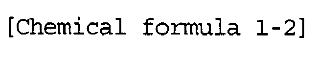

- where any one of R1, R2, R3, R4, R5, and R6 is CH3, and the remaining ones are H.
-

- Similarly, the B and C that are substituted or not substituted are given by chemical formula 1-4.
- [Chemical formula 1-4]

- Various forms of electron transport compounds can be formed by combining the pyrene based electron transport compound of chemical formula 1-1 with substituents of chemical formulas 1-2 to 1-4. The electron transport compounds can be easily selected by those skilled in the art according to necessity of brightness, color purity, or a driving voltage.
- This document provides organic light emitting device having the electron injecting and transport layer comprising the electron transport compound described above. The electron injecting and transport layer may be one or both of an electron injecting layer or an electron transport layer. The electron injecting and transport layer may be formed between an organic light emitting layer and a cathode. The electron injecting and transport layer may have a different layer position when participating in injecting and transporting of an electron as described above.
- Below, synthesis examples of some compounds of the pyrene based electron transport compounds of chemical formula 1-1 are described. Only synthesis examples of some compounds are described, but synthesis examples of other pyrene based electron transport compounds of chemical formula 1-1 are similar to these synthesis examples, the synthesis examples can be easily executed by those skilled in the art, and thus descriptions thereof will be omitted.
- [Synthesis Example]
- 1,5-di(4-(3'-pyridine)phenyl)-3,6-diphenylpyrene among electron transport compounds of an electron injecting and transport layer of organic light emitting device according to a first embodiment of this document is synthesized as follows.
- (1) Synthesis of 1,5-di(4-(3'-pyridine)-phenyl)pyrene
-

- 8.3g (0.0416mol) of 4-(3'-pyridine)phenyl boronic acid and 5g (0.0139mol) of 1,5-dibromopyrene were put in 100mL of anhydrous THF and they were stirred in a dried three neck round bottom flask.
- 1.0g of tetrakis(triphenylphosphine)palladium(0) and 15g of potassium carbonate were melted in 100mL of H2O and added to the flask. Then they were stirred for 24 hours in a bath of 100□ and when a reaction was ended, THF was removed from a reaction mixture.
- Thereafter, the reaction mixture was extracted using dichloromethane and water and distilled under a reduced pressure, then the distilled mixture was purified by passing through a silica gel column. The purified mixture was distilled under a reduced pressure again. The purified and distilled mixture was recrystallized using dichloromethane and methanol and filtered. Then 1,5-di(4-(3'-pyridine)-phenyl)pyrene was obtained.
- (2) Synthesis of 3,6-dibromo-1,5-di(4-(3'-pyridine)-phenyl)pyrene
-

- 1,5-di(4-(3'-pyridine)-phenyl)pyrene was put in 80mL of acetic acid and they were stirred in a dried three neck round bottom flask. After 1.9g (0.0118mol) of bromine (Br2) was added to the reaction mixture at a room temperature and when a reaction was ended, filtering was performed. By washing and then drying the reaction mixture with excessive distilled water, 3,6-dibromo-1,5-di(4-(3'-pyridine)-phenyl)pyrene was obtained.
- (3) Synthesis of 1,5-di(4-(3'-pyridine)phenyl)-3,6-diphenylpyrene
-
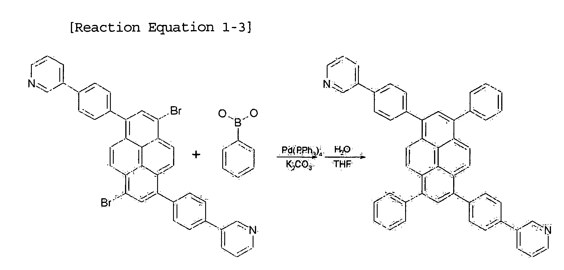
- 3g (0.0045mol) of 3,6-dibromo-1,5-di(4-(3'-pyridine)-phenyl)pyrene and 1.65g (0.0135mol) of phenyl boronic acid were put in 80mL of anhydrous THF and they are stirred in a dried three neck round bottom flask.
- 0.4g of tetrakis(triphenylphosphine)palladium(0) and 10g of potassium carbonate were melted in 80mL of H2O and added to the three neck round bottom flask. Then the reaction mixture was stirred for 24 hours in a bath of 100□ and when a reaction was ended, THF was removed from the reaction mixture.
- Thereafter, the reaction mixture was extracted using dichloromethane and water and distilled under a reduced pressure. The distilled mixture was purified by passing through a silica gel column, then distilled under a reduced pressure again. The purified and distilled mixture was recrystallized using dichloromethane and methanol and filtered. Then, 1,5-di(4-(3'-pyridine)phenyl)-3,6-diphenylpyrene, which is a final product was obtained.
- [Brightness, color purity and driving voltage test 1]
- In order to confirm brightness characteristic and color purity of organic light emitting device according to an embodiment of this document, conventional organic light emitting device and organic light emitting device according to an embodiment of this document were manufactured and brightness, color purity, and a driving voltage thereof were measured under the same condition.
- In other words, organic light emitting device according to an embodiment of this document was manufactured using the electron transport compound synthesized in the synthesis example and conventional organic light emitting device was manufactured using a conventional material in the electron injecting and transport layer. Then brightness, color purity, and a driving voltage thereof were measured under the same condition.
- In examples, although some electron transport compounds according to embodiments of this document are described, an organic light emitting device manufactured using other pyrene based electron transport compound of chemical formula 1-1 may show the same or similar result as examples. The result may be expected by those skilled in the art and thus descriptions of other compounds will be omitted.
- (1) A comparative example: Conventional organic light emitting device
- ITO glass was washed after being patterned so that a light emitting area thereof became 3mm X 3mm. After the substrate was mounted in a vacuum chamber, a hole injecting layer/a hole transport layer/a green organic emitting layer (host+dopant)/an electron injecting and transport layer/cathode (CuPc (650Å) /NPD(400Å) /Alq3(200Å) +GD-1(1%)(50Å)/Alq3(350Å)/LiF(5Å)/Al(1000Å)) were formed on ITO in 1.0X10⁻⁶torr.
- When current of 0.9mA was applied to the device, brightness was 1251cd/m2, a driving voltage was 6.5V, and a value of a color coordinate CIE was x = 0.307 and y = 0.612.
-


- (2) Example 1
- ITO glass was washed after being patterned so that a light emitting area thereof became 3mm X 3mm. After the substrate was mounted in a vacuum chamber, a hole injecting layer/a hole transport layer/a green organic emitting layer (host+dopant)/an electron injecting and transport layer/cathode (CuPc(650Å) /NPD(400Å) /Alq3 (200Å) +GD-1 (1%) (50Å) /PA-1(350Å)/LiF(5Å)/Al(1000Å)) were formed on ITO in 1.0X10⁻⁶ torr. PA-1 is a pyrene based electron transport compound of chemical formula 1-6.
- When current of 0.9mA was applied to the device, brightness was 2452cd/m2, a driving voltage was 4.7V, and a value of a color coordinate CIE was x = 0.301 and y = 0.606.
-

- (3) Example 2
- ITO glass was washed after being patterned so that a light emitting area thereof became 3mm X 3mm. After the substrate was mounted in a vacuum chamber, a hole injecting layer/a hole transport layer/a green organic emitting layer (host+dopant)/an electron injecting and transport layer/cathode CuPc (650Å) /NPD (400Å) /Alq3(200Å) +GD-1 (1%) (50Å) /PA-2(350Å)/LiF(5Å)/Al(1000Å) were formed on ITO in 1.0X10⁻⁶torr. PA-2 is a pyrene based electron transport compound of chemical formula 1-7.
- When current of 0.9mA was applied to the device, brightness was 2328cd/m2, a driving voltage was 5.0V, and a value of a color coordinate CIE was x = 0.302 and y = 0.612.
-

- (4) Example 3
- ITO glass was washed after being patterned so that a light emitting area thereof became 3mm X 3mm. After the substrate was mounted in a vacuum chamber, a hole injecting layer/a hole transport layer/a green organic emitting layer (host+dopant)/an electron injecting and transport layer/cathode (CuPc(650Å)/NPD(400Å)/Alq3(200Å)+GD-1(1%) (50Å)/PB-1(350Å)/LiF(5Å)/A1(1000Å)) were formed on ITO in 1.0X10⁻⁶torr. PB-1 is a pyrene based electron transport compound of chemical formula 1-8.
-

- When current of 0.9mA was applied to the device, brightness was 2751cd/m2, a driving voltage was 5.1V, and a value of a color coordinate CIE was x = 0.298 and y = 0.610.
- (5) Example 4
- ITO glass was washed after being patterned so that a light emitting area thereof became 3mm X 3mm. After the substrate was mounted in a vacuum chamber, a hole injecting layer/a hole transport layer/a green organic emitting layer (host+dopant)/an electron injecting and transport layer/cathode (CuPc (650Å) /NPD (400Å) /Alq3 (200Å) +GD-1 (1%) (50Å) /PC-1(350Å)/LiF(5Å)/Al(1000Å)) were formed on ITO in 1.0X10⁻⁶torr PC-1 is a pyrene based electron transport compound of chemical formula 1-9.
-

- When current of 0.9mA was applied to the device, brightness was 2617cd/m2, a driving voltage was 5.3V, and a value of a color coordinate CIE was x = 0.307 and y = 0.612.
- (6) Example 5
- ITO glass was washed after being patterned so that a light emitting area thereof became 3mm X 3mm. After the substrate was mounted in a vacuum chamber, a hole injecting layer/a hole transport layer/a green organic emitting layer (host+dopant)/an electron injecting and transport layer/cathode (CuPc(650Å)/NPD(400Å)/Alq3(200Å) +GD-1(1%) (50Å) /PE-1(350Å)/LiF(5Å)/Al(1000Å)) were formed on ITO in 1.0X10⁻⁶torr. PE-1 is a pyrene based electron transport compound of chemical formula 1-10.
-

- When current of 0.9mA was applied to the device, brightness was 2472cd/m2, a driving voltage was 5.4V, and a value of a color coordinate CIE was x = 0.31 and y = 0.614.
- (7) Example 6 - Organic light emitting device according to a sixth embodiment of this document
- ITO glass was washed after being patterned so that a light emitting area thereof became 3mm X 3mm. After the substrate was mounted in a vacuum chamber, a hole injecting layer/a hole transport layer/a green organic emitting layer (host+dopant)/an electron injecting and transport layer/cathode (CuPc(650Å) /NPD(400Å) /Alq3 (200Å) +GD-1 (1%) (50Å) /PF-1(350Å)/LiF(5Å)/Al(1000Å)) were formed on ITO in 1.0X10⁻⁶ torr. PF-1 is a pyrene based electron transport compound of chemical formula 1-11.
-

- When current of 0. 9mA was applied to the device, brightness was 2217cd/m2, a driving voltage was 5.5V, and a value of a color coordinate CIE was x = 0.302 and y = 0.610.
- (8) Example 7 - Organic light emitting device according to a seventh embodiment of this document
- ITO glass was washed after being patterned so that a light emitting area thereof became 3mm X 3mm. After the substrate was mounted in a vacuum chamber, a hole injecting layer/a hole transport layer/a green organic emitting layer (host+dopant)/an electron injecting and transport layer/cathode (CuPc (650Å) /NPD(400Å) /Alq3(200Å) +GD-1 (1%) (50Å) /PK-1(350Å)/LiF(5Å)/Al(1000Å)) were formed on ITO in 1.0X10⁻⁶torr. PK-1 is a pyrene based electron transport compound of chemical formula 1-12.
-

- When current of 0.9mA was applied to the device, brightness was 2830cd/m2, a driving voltage was 5.0V, and a value of a color coordinate CIE was x = 0.297 and y = 0.609.
- As can be seen in the comparative example and examples, when organic light emitting device according to embodiments of this document comprise pyrene based electron transport compound of chemical formula 1-1 described above in an electron injecting and transport layer, a value of a color coordinate CIE was x = 0.397 to 0.307 and y = 0.606 to 0.612, and thus it can be seen that an electron injecting and transport layer performs its own function very effectively.
- Referring to Table 1, brightness of organic light emitting device according to embodiments of this document improves by minimum 77.2% (the sixth embodiment) and maximum 26% (the seventh embodiment), compared to brightness of conventional organic light emitting device. It can be seen that a driving voltage of organic light emitting device according to embodiments of this document was decreased to 4.7V to 5.5V, compared to a driving voltage of conventional organic light emitting device.
-
[Table 1] brightness driving voltage Comparative example 1251cd/m2 6.5V Example 1 2452cd/m2 4.7V Example 2 2328cd/m2 5.0V Example 3 2751cd/m2 5.1V Example 4 2617cd/m2 5.3V Example 5 2472cd/m2 5.4V Example 6 2217cd/m2 5.5V Example 7 2830cd/m2 5.0V - Embodiment 2
- In order to achieve the object, this document provides a pyrene based electron transport compound having chemical formula 2-1.
-

- Pyrene based compound of chemical formula 2-1 is a very important compound among hydrocarbons. In the pyrene based compound, carbons are numbered clockwise starting with a carbon having a substituent A-C. Accordingly, an electron transport compound according to an embodiment of this document comprises a pyrene based compound in which A-C is bonded to carbon 1 and B is bonded to carbon 3, 6 and 8. The substituents A, B, and C may be substituted or not substituted.
- The electron transport compound is a compound that injects an electron from a cathode to other layer or transports an injected electron to other layers. For example, in organic light emitting device, an electron transport compound is a compound that may be a material of an electron injecting layer, an electron transport layer, or an electron injecting and transport layer in which the electron injecting layer and the electron transport layer are mixed.
- In this document, the electron injecting and transport layer is used to generally designate layers, which are related to injecting and transporting of an electron, such as an electron injecting layer, an electron transport layer, or an electron injecting and transport layer in which the electron injecting layer and the electron transport layer are mixed.
- A that is substituted or is not substituted may be selected from a group consisting of pyridinyl, quinolinyl, isoquinolinyl, quinoxalinyl, bipyridinyl, terpyridinyl, and phenanthrolinyl.
- Further, B and C that are substituted or are not substituted may be selected from a group consisting of phenyl, biphenyl, naphthyl, fluorenyl, terphenyl, phenanthrolinyl, phenanthryl, and anthryl.
- When the A, B, and C are substituted, a substituent of the A, B, and C may be selected from a group consisting of aryl, alkyl, aryloxy, alkoxy, allylamino, alkylamino, halogen, and cyano.
- Further, when the A, B, and C are substituted, a substituent of the A, B, and C may be selected from a group consisting of phenyl, biphenyl, triphenylmethyl, phenylethylidene, diphenylethylidene, phenylmethylidyne, phenoxy, tolyoxy, methyl, ethyl, propyl, i-propyl, t-butyl, cyclohexyl, diphenylamino, morpholine, methoxy, ethoxy, propoxy, butoxy, dimethylamino, diphenylamino, fluorine, and chlorine.
- The A that is substituted or is not substituted is given by chemical formulas 2-2 and 2-3.
-


- where any one of R1, R2, R3, R4, R5, and R6 is CH3, and the remaining ones are H.
-

- Similarly, the B and C that are substituted or not substituted are given by chemical formula 2-4.
- [Chemical formula 2-4]

- Various forms of electron transport compounds can be formed by combining the pyrene based electron transport compound of chemical formula 2-1 with substituents of chemical formulas 2-2 to 2-4. The electron transport compounds can be easily selected from organic light emitting device such as organic light emitting device by those skilled in the art according to necessity of brightness, color purity, or a driving voltage.
- This document provides organic light emitting device having the electron injecting and transport layer comprising the electron transport compound described above. The electron injecting and transport layer may be one or both of an electron injecting layer or an electron transport layer. The electron injecting and transport layer may be formed between an organic or inorganic light emitting layer and a cathode. The electron injecting and transport layer may have a different layer position when participating in injecting and transporting of an electron as described above.
- Below, synthesis examples of some compounds of the pyrene based electron transport compounds of chemical formula 2-1 are described. Only synthesis examples of some compounds are described, but synthesis examples of other pyrene based electron transport compounds of chemical formula 2-1 are similar to these synthesis examples, the synthesis examples can be executed by those skilled in the art, and thus descriptions thereof will be omitted.
- [Synthesis Example]
- 1-(4-(3'-pyridine)phenyl)-3,6,8-triphenylpyrene among electron transport compounds of an electron injecting and transport layer of organic light emitting device according to an embodiment of this document is synthesized as follows.
- (1) Synthesis of 1-(4-(3'-pyridine)phenyl)pyrene
-

- 5.31g (0.0267mol) of 4-(3'-pyridine) phenyl boronic acid and 5g (0.0178mol) of 1-bromopyrene were put in 100mL of anhydrous THF and they were stirred in a dried three neck round bottom flask.
- 1.0g of tetrakis(triphenylphosphine)palladium(0) and 15g of potassium carbonate were melted in 100mL of H2O and added to the flask. Then they were stirred for 24 hours in a bath of 100□ . When a reaction was ended, THF was removed from a reaction mixture.
- Thereafter, the reaction mixture was extracted using dichloromethane and water and distilled under a reduced pressure then the distilled mixture was purified by passing through a silica gel column. The purified mixture was distilled under a reduced pressure again. The purified and distilled mixture was recrystallized using dichloromethane and methanol and filtered. Then 1-(4-(3'-pyridine)-phenyl)pyrene was obtained.
- (2) Synthesis of 1-(4-(3'-pyridine)-phenyl)-3,6,8-tribromopyrene
-

- 3g (0.0084mol) of 1-(4-(3'-pyridine)-phenyl)pyrene was put in 80mL of acetic acid and they were stirred in a dried three neck round bottom flask. After 4.0g (0.0252mol) of bromine (Br2) was added to the reaction mixture at a room temperature and when a reaction was ended, filtering was performed. By washing and then drying the reaction mixture with excessive distilled water, 1-(4-(3'-pyridine)-phenyl)-3,6,8-tribrmopyrene was obtained.
- (3) Synthesis of 1-(4-(3'-pyridine)phenyl)-3,6,8-triphenylpyrene
-

- 3g (0.00506mol) of 1-(4-(3'-pyridine)-phenyl)-3,6,8-tribromophylene and 2.47g (0.0202mol) of phenyl boronic acid were put in 80mL of anhydrous THF and they were stirred in a dried three neck round bottom flask.
- 0.4g of (tetrakis(triphenylphosphine)palladium)(0) and 10g of potassium carbonate were melted in 80mL of H2O and added to the flask. Then they were stirred for 24 hours in a bath of 100□ . When a reaction was ended, THF was removed from a reaction mixture.
- Thereafter, the reaction mixture was extracted using dichloromethane and water and distilled under a reduced pressure then the distilled mixture was purified by passing through a silica gel column. The purified mixture was distilled under a reduced pressure again. The purified and distilled mixture was recrystallized using dichloromethane and methanol and filtered. Then 1-(4-(3'-pyridine)-phenyl)-3,6,8-triphenylenepyrene was obtained.
- [Brightness, color purity and driving voltage test 2]
- In order to confirm brightness characteristic and color purity of organic light emitting device according to an embodiment of this document, conventional organic light emitting device and organic light emitting device according to an embodiment of this document were manufactured and brightness, color purity, and a driving voltage thereof were measured under the same condition.
- In other words, organic light emitting device according to an embodiment of this document was manufactured using the electron transport compound synthesized in the synthesis example and conventional organic light emitting device was manufactured using a conventional material in the electron injecting and transport layer. Then brightness, color purity, and a driving voltage thereof were measured under the same condition.
- In examples, although some electron transport compounds according to embodiments of this document are described, an organic light emitting device manufactured using other pyrene based electron transport compound of chemical formula 1-1 may show the same or similar result as examples. The result may be expected by those skilled in the art and thus descriptions of other compounds will be omitted.
- (1) A comparative example: Conventional organic light emitting device
- ITO glass was washed after being patterned so that a light emitting area thereof became 3mm X 3mm. After the substrate was mounted in a vacuum chamber, a hole injecting layer/a hole transport layer/a green organic emitting layer (host+dopant)/an electron injecting and transport layer/cathode (CuPc(650Å) /NPD(400Å) /Alq3(200Å) +GD-1(1%) (50Å)/Alq3(350Å)/LiF(5Å)/Al(1000Å)) were formed on ITO in 1.0X10⁻⁶torr.
- When current of 0.9mA was applied to the device, brightness was 1251cd/m2, a driving voltage was 6.5V, and a value of a color coordinate CIE was x = 0.307 and y = 0.612.
-


- (2) Example 1
- ITO glass was washed after being patterned so that a light emitting area thereof became 3mm X 3mm. After the substrate was mounted in a vacuum chamber, a hole injecting layer/a hole transport layer/a green organic emitting layer (host+dopant)/an electron injecting and transport layer/cathode (CuPc (650Å) /NPD (400Å) /Alq3 (200Å) +GD-1 (1%) (50Å) /TPA-1(350Å)/LiF(5Å)/Al(1000Å)) were formed on ITO in 1.0X10⁻⁶torr. TPA-1 is an electron transport compound of 1-(4-(3'-pyridine)phenyl)-3,6,8-trhenylpyrene of chemical formula 2-6 in which A is pyridine and B and C are phenyl.
- When current of 0.9mA was applied to the device, brightness was 2511/m2, a driving voltage was 5.1V, and a value of a color coordinate CIE was x = 0.301 and y = 0.610.
-
- (3) Example 2
- ITO glass was washed after being patterned so that a light emitting area thereof became 3mm X 3mm. After the substrate was mounted in a vacuum chamber, a hole injecting layer/a hole transport layer/a green organic emitting layer (host+dopant)/an electron injecting and transport layer/cathode CuPc(650Å) /NPD (400Å) /Alq3(200Å) +GD-1 (1%) (50Å) /TPB-1(350Å)/LiF(5Å)/Al(1000Å)were formed on ITO in 1.0X10⁻⁶torr. TPB-8 is a pyrene based electron transport compound of chemical formula 2-7 in which A is pyridine, B is biphenyl and C is phenyl.
- When current of 0.9mA was applied to the device, brightness was 2830cd/m2, a driving voltage was 5.1V, and a value of a color coordinate CIE was x = 0.300 and y = 0.607.
-
- (4) Example 3
- ITO glass was washed after being patterned so that a light emitting area thereof became 3mm X 3mm. After the substrate was mounted in a vacuum chamber, a hole injecting layer/a hole transport layer/a green organic emitting layer (host+dopant)/an electron injecting and transport layer/cathode (CuPc (650Å) /NPD (400Å) /Alq3 (200Å) +GD-1 (1%) (50Å) /TPC-1(350Å)/LiF(5Å)/Al(1000Å)) were formed on ITO in 1.0X10⁻⁶torr. TPC-1 is a pyrene based electron transport compound of chemical formula 2-8.
-

- When current of 0.9mA was applied to the device, brightness was 2770cd/m2, a driving voltage was 5.3V, and a value of a color coordinate CIE was x = 0.302 and y = 0.611.
- (5) Example 4
- ITO glass was washed after being patterned so that a light emitting area thereof became 3mm X 3mm. After the substrate was mounted in a vacuum chamber, a hole injecting layer/a hole transport layer/a green organic emitting layer (host+dopant)/an electron injecting and transport layer/cathode (CuPc (650Å) /NPD (400Å) /Alq3 (200Å) +GD-1 (1%) (50Å) /TPE-1(350Å)/LiF(5Å)/Al(1000Å)) were formed on ITO in 1.0X10⁻⁶torr TPE-1 is a pyrene based electron transport compound of chemical formula 2-9.
-
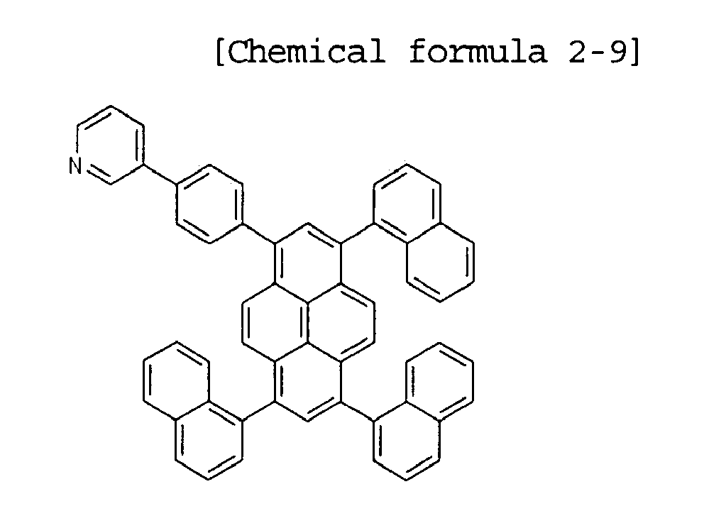
- When current of 0.9mA was applied to the device, brightness was 2069cd/m2, a driving voltage was 5.5V, and a value of a color coordinate CIE was x = 0.304 and y = 0.614.
- (6) Example 5
- ITO glass was washed after being patterned so that a light emitting area thereof became 3mm X 3mm. After the substrate was mounted in a vacuum chamber, a hole injecting layer/a hole transport layer/a green organic emitting layer (host+dopant)/an electron injecting and transport layer/cathode (CuPc(650Å)/NPD(400Å)/Alq3(200Å) +GD-1 (1%) (50Å) /TPF-1(350Å)/LiF(5Å)/Al(1000Å)) were formed on ITO in 1.0X10⁻⁶torr. TPF-1 is a pyrene based electron transport compound of chemical formula 2-10.
-
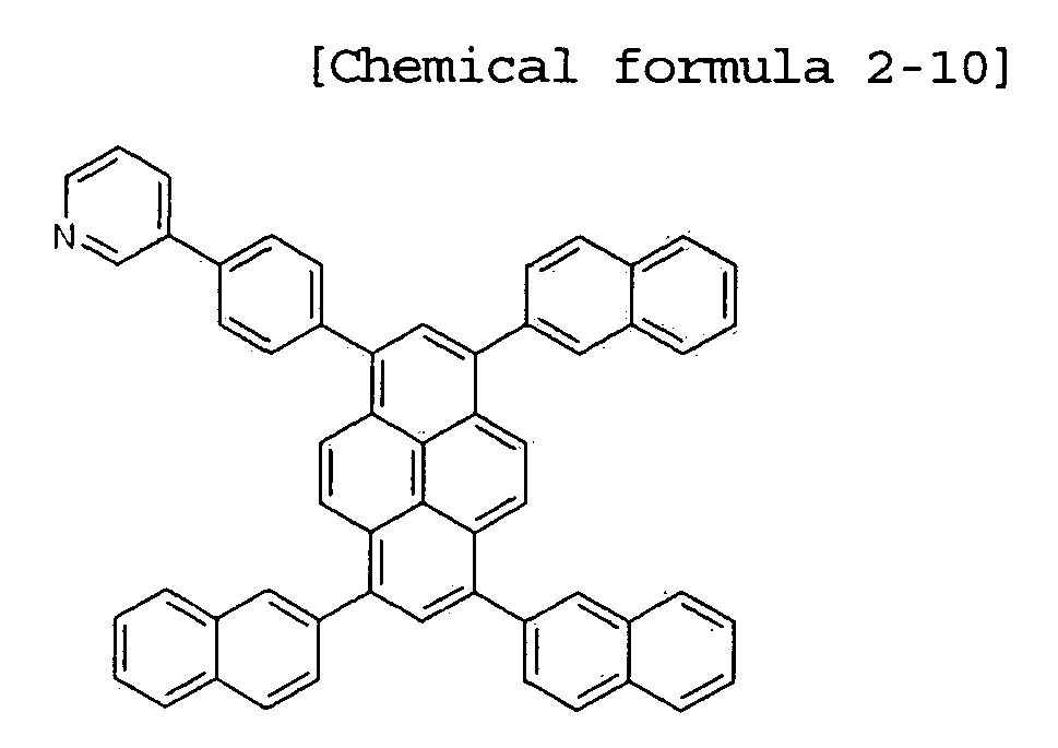
- When current of 0.9mA was applied to the device, brightness was 2466cd/m2, a driving voltage was 5.7V, and a value of a color coordinate CIE was x = 0.300 and y = 0.610.
- (7) Example 6
- ITO glass was washed after being patterned so that a light emitting area thereof became 3mm X 3mm. After the substrate was mounted in a vacuum chamber, a hole injecting layer/a hole transport layer/a green organic emitting layer (host+dopant)/an electron injecting and transport layer/cathode (CuPc(650Å) /NPD(400Å) /Alq3 (200Å) +GD-1(1%) (50Å) /TPK-1(350Å)/LiF(5Å)/Al(1000Å)) were formed on ITO in 1.0X10⁻⁶ torr. TPK-1 is a pyrene based electron transport compound of chemical formula 2-11.
-
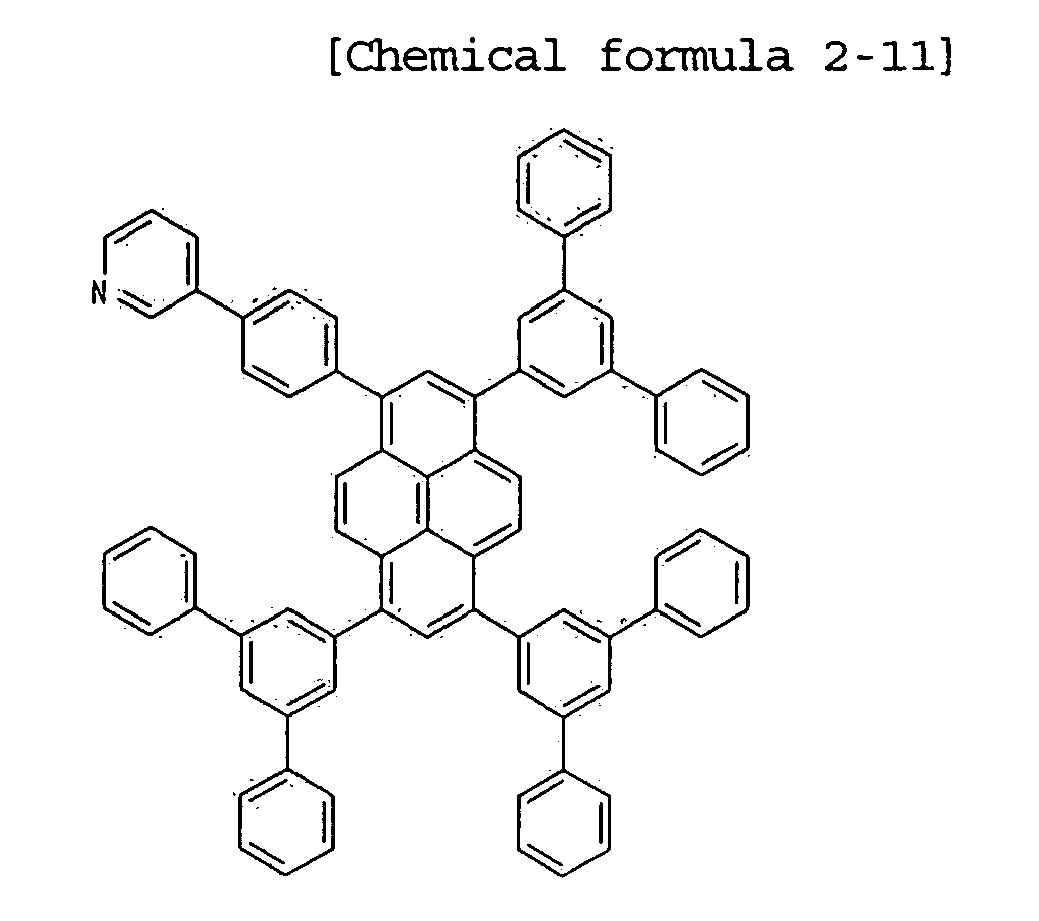
- When current of 0.9mA was applied to the device, brightness was 2750cd/m2, a driving voltage was 5.2V, and a value of a color coordinate CIE was x = 0.302 and y = 0.610.
- As can be seen in a comparative experiment example, when organic light emitting device according to embodiments of this document use the pyrene based electron transport compound of chemical formula 2-1 described above in an electron injecting and transport layer, a value of a color coordinate CIE was x = 0.300 to 0.307 and y = 0.607 to 0.614, and thus it can be seen that an electron injecting and transport layer performs its own function.
- As can be seen in Table 2, brightness of organic light emitting device according to embodiments of this document improves by minimum 77.2% (the sixth embodiment) and maximum 26% (the seventh embodiment), compared to brightness of conventional organic light emitting device. It can be seen that a driving voltage of organic light emitting device according to embodiments of this document was decreased to 5.1V to 5.7V.
- [Table 2]
brightness driving voltage Comparative example 1251cd/m2 6.5V Example 1 2511cd/m2 5.1V Example 2 2830cd/m2 5.1V Example 3 2770cd/m2 5.3V Example 4 2069cd/m2 5.5V Example 5 2466cd/m2 5.7V Example 6 2750cd/m2 5.2V - Embodiment 3
- In order to achieve the object, this document provides a pyrene based electron transport compound having chemical formula 3-1.
-

- Pyrene based compound of chemical formula 3-1 is a very important compound among hydrocarbons. In the pyrene based compound, carbons are numbered clockwise starting with a carbon having a substituent A. Accordingly, an electron transport compound according to an embodiment of this document comprises a pyrene based compound in which A is bonded to carbon 1, and B is bonded to carbon 3,6 and 8. The substituents A and B may be substituted or not substituted.
- The electron transport compound is a compound that injects an electron from a cathode to other layer or transports an injected electron to other layers. For example, in organic light emitting device, an electron transport compound is a compound that may be a material of an electron injecting layer, an electron transport layer, or an electron injecting and transport layer in which the electron injecting layer and the electron transport layer are mixed.
- In this document, an electron injecting and transport layer is used to generally designate layers, which are related to injecting and transporting of an electron, such as an electron injecting layer, an electron transport layer, or an electron injecting and transport layer in which the electron injecting layer and the electron transport layer are mixed.
- A that is substituted or is not substituted may be selected from a group consisting of pyridinyl, quinolinyl, isoquinolinyl, quinoxalinyl, bipyridinyl, terpyridinyl, and phenanthrolinyl.
- Further, B and C that are substituted or are not substituted may be selected from a group consisting of phenyl, biphenyl, naphthyl, fluorenyl, terphenyl, methyl, ethyl, propyl, i-propyl, halogen, phenanthrolinyl, phenanthryl, and anthryl.
- When the A and B are substituted, a substituent of the A and B may be selected from a group consisting of aryl, alkyl, aryloxy, alkoxy, allylamino, alkylamino, halogen, and cyano.
- Further, when the A and B are substituted, a substituent of the A and B may be selected from a group consisting of phenyl, biphenyl, triphenylmethyl, phenylethylidene, diphenylethylidene, phenylmethylidyne, phenoxy, tolyoxy, methyl, ethyl, propyl, i-propyl, t-butyl, cyclohexyl, diphenylamino, morpholine, methoxy, ethoxy, propoxy, butoxy, dimethylamino, diphenylamino, fluorine, and chlorine.
- The A that is substituted or is not substituted is given by chemical formulas 3-2 and 3-3.
-


- where any one of R1, R2, R3, R4, R5, and R6 is CH3, and the remaining ones are H.
-

- Similarly, the B that is substituted or not substituted is given by chemical formula 3-4.
-


- Various forms of electron transport compounds can be formed by combining the pyrene based electron transport compound of chemical formula 3-1 with substituents of chemical formulas 3-2 to 3-4. The electron transport compounds can be easily selected by those skilled in the art according to necessity of brightness, color purity, or a driving voltage.
- This document provides organic light emitting device having the electron injecting and transport layer comprising the electron transport compound described above. The electron injecting and transport layer may be one or both of an electron injecting layer or an electron transport layer. The electron injecting and transport layer may be formed between an organic or inorganic light emitting layer and a cathode. The electron injecting and transport layer may have a different layer position when participating in injecting and transporting of an electron as described above.
- Below, synthesis examples of some compounds of the pyrene based electron transport compounds of chemical formula 3-1 are described. Only synthesis examples of some compounds are described, but synthesis examples of other pyrene based electron transport compounds of chemical formula 3-1 are similar to these synthesis examples, the synthesis examples can be executed by those skilled in the art, and thus descriptions thereof will be omitted.
- [Synthesis Example]
- 1-(3'-pyridine)-3,6,8-triphenyl-pyrene among electron transport compounds of an electron injecting and transport layer of organic light emitting device according to an embodiment of this document is synthesized as follows.
- Synthesis of 1-(3'-pyridine)pyrene
-

- 6.56g (0.053mol) of pyridinyl boronic acid and 5g (0.0178mol) of 1-bromopyrene were put in 100mL of anhydrous THF and they were stirred in a dried three neck round bottom flask.
- 0.9g of (tetrakis (triphenylphosphine) palladium) (0) and 15g of potassium carbonate were melted in 100mL of H2O added to the flask. Then they were stirred for 24 hours in a bath of 100□ and then when a reaction was ended, THF was removed from the reaction mixture.
- Thereafter, the reaction mixture was extracted using dichloromethane and water and distilled under a reduced pressure, then the distilled mixture was purified by passing through a silica gel column. The purified mixture was distilled under a reduced pressure again. The purified and distilled mixture was recrystallized using dichloromethane and methanol and filtered. Then 1-(3'-pyridine)pyrene was obtained.
- (2) Synthesis of 1-(3'-pyridine)-3,4,6-tribromopyrene
-

- 3g (0.0107mol) of 1-(3'-pyridine)pyrene was put in 80mL of acetic acid and was stirred in a dried three neck round bottom flask. After 5.15g (0.0322mol) of bromine (Br2) was added to the reaction mixture at a room temperature and when a reaction was ended, filtering was performed. By washing and then drying the reaction mixture with excessive distilled water, 1-(3'-pyridine)-3,6,8,-tribromopyrene was obtained.
- (3) Synthesis of 1-(3'-pyridine)-3,6,8,-triphenyl-pyrene
-

- 3g (0.00581mol) of 1-(3'-pyridine)-3,6,8,-tribromopyrene and 2.83g (0.0232mol) of phenyl boronic acid were put in 80mL of anhydrous THF and they were stirred in a dried three neck round bottom flask.
- 0.5g of (tetrakis(triphenylphosphine) palladium) (0) and 10g of potassium carbonate were melted in 80mL of H2O and H2O and added to the flask. Then they were stirred for 24 hours in a bath of 100□ and when a reaction was ended, THF was removed from the reaction mixture.
- Thereafter, the reaction mixture was extracted using dichloromethane and water and distilled under a reduced pressure, then distilled mixture was purified by passing through a silica gel column. The purified mixture was distilled under a reduced pressure again. The purified and distilled mixture was recrystallized using dichloromethane and methanol and filtered. 1-(3'-pyridine)-3,6,8-triphenyl-pyrene, which is a final product was obtained.
- [Brightness, color purity and driving voltage test 3]
- In order to confirm brightness characteristic and color purity of organic light emitting device according to an embodiment of this document, conventional organic light emitting device and organic light emitting device according to an embodiment of this document were manufactured and brightness, color purity, and a driving voltage thereof were measured under the same condition.
- In other words, organic light emitting device according to an embodiment of this document was manufactured using the electron transport compound synthesized in the synthesis example and conventional organic light emitting device was manufactured using a conventional material in the electron injecting and transport layer. Then brightness, color purity, and a driving voltage thereof were measured under the same condition.
- In examples, although some electron transport compounds according to embodiments of this document are described, an organic light emitting device manufactured using other pyrene based electron transport compound of chemical formula 1-1 may show the same or similar result as examples. The result may be expected by those skilled in the art and thus descriptions of other compounds will be omitted.
- (1) A comparative example: Conventional organic light emitting device
- ITO glass was washed after being patterned so that a light emitting area thereof became 3mm X 3mm. After the substrate was mounted in a vacuum chamber, a hole injecting layer/hole transport layer/green color organic emitting layer (host+dopant)/electron injecting and transport layer/cathode (CuPc(650Å)/NPD(400Å)/Alq3(200Å)+GD- 1(1%)(50Å)/Alq3(350Å)/LiF(5Å)/Al(1000Å)) was formed on ITO in 1.0X10⁻⁶torr.
- When current of 0.9mA was applied to the device, brightness was 1251cd/m2, a driving voltage was 6.5V, and a value of a color coordinate CIE was x = 0.307 and y = 0.612.
-
- (2) Example 1
- ITO glass was washed after being patterned so that a light emitting area thereof became 3mm X 3mm. After the substrate was mounted in a vacuum chamber, a hole injecting layer/a hole transport layer/a green organic emitting layer (host+dopant)/an electron injecting and transport layer/cathode (CuPc(650Å) /NPD(400Å) /Alq3(200Å) +GD-1(1%) (50Å) /TA-8(350Å)/LiF(5Å)/Al(1000Å)) were formed on ITO in 1.0X10⁻⁶torr. TA-8 is an electron transport compound of 1-(3'-pyridine)-3,6,8-triphenyl-pyrene of chemical formula 3-6 in which A is pyridine and B and C are phenyl.
- When current of 0.9mA was applied to the device, brightness was 2403cd/m2, a driving voltage was 5.87V, and a value of a color coordinate CIE was x = 0.301 and y = 0.621.
-

- (3) Example 2
- ITO glass was washed after being patterned so that a light emitting area thereof became 3mm X 3mm. After the substrate was mounted in a vacuum chamber, , a hole injecting layer/a hole transport layer/a green organic emitting layer (host+dopant)/an electron injecting and transport layer/cathode (CuPc(650Å)/NPD(400Å)/Alq3(200Å)+GD-1(1%) (50Å)/TB-8(350Å)/LiF(5Å)/Al(1000Å)) were formed on ITO in 1.0X10⁻⁶torr. TB-8 is a pyrene based electron transport compound of chemical formula 3-7 in which A is pyridine and B and C are phenyl.
- When current of 0.9mA was applied to the device, brightness was 2511cd/m2, a driving voltage was 5.7V, and a value of a color coordinate CIE was x = 0.301 and y = 0.607.
-

- (4) Example 3
- ITO glass was washed after being patterned so that a light emitting area thereof became 3mm X 3mm. After the substrate was mounted in a vacuum chamber, a hole injecting layer/a hole transport layer/a green organic emitting layer (host+dopant)/an electron injecting and transport layer/cathode (CuPc(650Å) / NPD(400Å) / Alq3(200Å)+GD-1(1%) (50Å) / TB-7(350Å)/LiF(5Å)/Al(1000Å)) were formed on ITO in 1.0X10⁻⁶ torr. TB-7 is a pyrene based electron transport compound of chemical formula 3-8 in which A is pyridine and B is phenyl.
-


- When current of 0.9mA was applied to the device, brightness was 2398cd/m2, a driving voltage was 5.3V, and a value of a color coordinate CIE was x = 0.304 and y = 0.630.
- (5) Example 4
- ITO glass was washed after being patterned so that a light emitting area thereof became 3mm X 3mm. After the substrate was mounted in a vacuum chamber, , a hole injecting layer/a hole transport layer/a green organic emitting layer (host+dopant)/an electron injecting and transport layer/cathode (CuPc (650Å) /NPD (400Å) /Alq3 (200Å) +GD-1 (1%) (50Å) /TC-8(350Å)/LiF(5Å)/Al(1000Å)) were formed on ITO in 1.0X10⁻⁶torr. TC-8 is a pyrene based electron transport compound of chemical formula 3-9.
-

- When current of 0.9mA was applied to the device, brightness was 2382cd/m2, a driving voltage was 5.6V, and a value of a color coordinate CIE was x = 0.299 and y = 0.617.
- (6) Example 5
- ITO glass was washed after being patterned so that a light emitting area thereof became 3mm X 3mm. After the substrate was mounted in a vacuum chamber, a hole injecting layer/a hole transport layer/a green organic emitting layer (host+dopant)/an electron injecting and transport layer/cathode (CuPc (650Å) /NPD (400Å) /Alq3(200Å) +GD-1 (1%) (50Å) /TD-8(350Å)/LiF(5Å)/Al(1000Å)) were formed on ITO in 1.0X10⁻⁶ torr. TD-8 is a pyrene based electron transport compound of chemical formula 3-10.
-

- When current of 0.9mA was applied to the device, brightness was 2698cd/m2, a driving voltage was 5.5V, and a value of a color coordinate CIE was x = 0.300 and y = 0.638.
- (7) Example 6
- ITO glass was washed after being patterned so that a light emitting area thereof became 3mm X 3mm. After the substrate was mounted in a vacuum chamber, a hole injecting layer/a hole transport layer/a green organic emitting layer (host+dopant)/an electron injecting and transport layer/cathode (CuPc (650Å) /NPD (400Å) /Alq3(200Å) +GD-1 (1%) (50Å)/TE-8(350Å)/LiF(5Å)/Al(1000Å)) were formed on ITO in 1.0X10⁻⁶torr. TE-8 is a pyrene based electron transport compound of chemical formula 3-11.
-

- When current of 0.9mA was applied to the device, brightness was 2732cd/m2, a driving voltage was 5.4V, and a value of a color coordinate CIE was x = 0.300 and y = 0.610.
- (8) Example 7
- ITO glass was washed after being patterned so that a light emitting area thereof became 3mm X 3mm. After the substrate was mounted in a vacuum chamber, a hole injecting layer/a hole transport layer/a green organic emitting layer (host+dopant)/an electron injecting and transport layer/cathode (CuPc (650Å) /NPD(400Å) /Alq3(200Å) +GD-1(1%)(50Å) /TF-8(350Å)/LiF(5Å)/Al(1000Å)) were formed on ITO in 1.0X10⁻⁶torr. TF-8 is a pyrene based electron transport compound of chemical formula 3-12.
-

- When current of 0.9mA was applied to the device, brightness was 2287cd/m2, a driving voltage was 5.5V, and a value of a color coordinate CIE was x = 0.300 and y = 0.618.
- (9) Example 8
- ITO glass was washed after being patterned so that a light emitting area thereof became 3mm X 3mm. After the substrate was mounted in a vacuum chamber a hole injecting layer/a hole transport layer/a green organic emitting layer (host+dopant)/an electron injecting and transport layer/cathode (CuPc (650Å) /NPD(400Å) /Alq3 (200Å) +GD-1 (1%) (50Å) /TG-8(350Å)/LiF(5Å)/Al(1000Å)) were formed on ITO in 1.0X10⁻⁶torr. TG-8 is a pyrene based electron transport compound of chemical formula 3-13.
-


- When current of 0.9mA was applied to the device, brightness was 2096cd/m2, a driving voltage was 5.7V, and a value of a color coordinate CIE was x = 0.304 and y = 0.629.
- (10) Example 9
- ITO glass was washed after being patterned so that a light emitting area thereof became 3mm X 3mm. After the substrate was mounted in a vacuum chamber, a hole injecting layer/a hole transport layer/a green organic emitting layer (host+dopant)/an electron injecting and transport layer/cathode (CuPc(650Å)/NPD(400Å)/Alq3(200Å)+GD-1 (1%) (50Å)/TJ-8(350Å)/LiF(5Å)/Al(1000Å)) were formed on ITO in 1.0X10⁻⁶torr. TJ-8 is a pyrene based electron transport compound of chemical formula 3-14.
-

- When current of 0.9mA was applied to the device, brightness was 2937cd/m2, a driving voltage was 6.1V, and a value of a color coordinate CIE was x = 0.307 and y = 0.609.
- As can be seen in the comparative example and examples, when organic light emitting devices according to embodiments of this document comprise the pyrene based electron transport compound of chemical formula 3-1 described above in an electron injecting and transport layer, a value of a color coordinate CIE was x = 0.300 to 0.307 and y = 0.600 to 0.630, and thus it can be seen that an electron injecting and transport layer performs its own function.
- Referring to Table 3, brightness of organic light emitting device according to embodiments of this document improves by minimum 67.5% (the eighth embodiment) and maximum 135% (the ninth embodiment), compared to brightness of conventional organic light emitting device. It can be seen that a driving voltage of organic light emitting device according to embodiments of this document was decreased to 5.4V to 5.8V, compared to a driving voltage of conventional organic light emitting device.
-
[Table 3] brightness driving voltage Comparative example 1251cd/m2 6.5V Example 1 2403cd/m2 5.8V Example 2 2511cd/m2 5.7V Example 3 2398cd/m2 5.3V Example 4 2382cd/m2 5.6V Example 5 2698cd/m2 5.5V Example 6 2732cd/m2 5.4V Example 7 2287cd/m2 5.5V Example 8 2096cd/m2 5.7V Example 9 2937cd/m2 6.1V - As described above, this document can provide an electron transport compound that has high electron transport efficiency and good deposition characteristics, prevents crystallization, and has no influence on a lifetime of diodes.
- As a result, organic light emitting device according to embodiments of this document can have improved brightness and a considerably low driving voltage while performing a function as an electron injecting and transport layer, compared to conventional organic light emitting device.
- Embodiments are described, but this document is not limited thereto.
- The invention being thus described, it will be obvious that the same may be varied in many ways. Such variations are not to be regarded as a departure from the spirit and scope of the invention, and all such modifications as would be obvious to one skilled in the art are intended to be comprised within the scope of the following claims.
Claims (18)
- An electron transport compound, having the following chemical formula,
wherein A that is substituted or is not substituted is selected from a group consisting of pyridinyl, quinolinyl, isoquinolinyl, quinoxalinyl, bipyridinyl, terpyridinyl, and phenanthrolinyl, and
B and C that are substituted or are not substituted are selected from a group consisting of phenyl, biphenyl, naphthyl, fluorenyl, terphenyl, phenanthrolinyl, phenanthryl, and anthryl.
- The electron transport compound of claim 1, wherein when the A, B, and C are substituted, a substituent of the A, B, and C is selected from a group consisting of aryl, alkyl, aryloxy, alkoxy, allylamino, alkylamino, halogen, and cyano.
- The electron transport compound of claim 1, wherein when the A, B, and C are substituted, a substituent of the A, B, and C is selected from a group consisting of phenyl, biphenyl, triphenylmethyl, phenylethylidene, diphenylethylidene, phenylmethylidyne, phenoxy, tolyoxy, methyl, ethyl, propyl, i-propyl, t-butyl, cyclohexyl, diphenylamino, morpholine, methoxy, ethoxy, propoxy, butoxy, dimethylamino, diphenylamino, fluorine, and chlorine.
- An organic light emitting device having an electron injecting and transport layer comprising the electron transport compound of Claim 1.
- The organic light emitting device of claim 4, wherein the electron injecting and transport layer is one or both of an electron injecting layer or an electron transport layer.
- The organic light emitting device of claim 5, wherein the organic light emitting device comprises an anode, an emitting layer comprising an organic material and a cathode,
wherein the electron injecting and transport layer is formed between the emitting layer and a cathode. - An electron transport compound, having the following chemical formula,
wherein A that is substituted or is not substituted is selected from a group consisting of pyridinyl, quinolinyl, isoquinolinyl, quinoxalinyl, bipyridinyl, terpyridinyl, and phenanthrolinyl, and
B and C that are substituted or are not substituted are selected from a group consisting of phenyl, biphenyl, naphthyl, fluorenyl, terphenyl, phenanthrolinyl, phenanthryl, and anthryl.
- The electron transport compound of claim 7, wherein when the A, B, and C are substituted, a substituent of the A, B, and C is selected from a group consisting of aryl, alkyl, aryloxy, alkoxy, allylamino, alkylamino, halogen, and cyano.
- The electron transport compound of claim 7, wherein when the A, B, and C are substituted, a substituent of the A, B, and C is selected from a group consisting of phenyl, biphenyl, triphenylmethyl, phenylethylidene, diphenylethylidene, phenylmethylidyne, phenoxy, tolyoxy, methyl, ethyl, propyl, i-propyl, t-butyl, cyclohexyl, diphenylamino, morpholine, methoxy, ethoxy, propoxy, butoxy, dimethylamino, diphenylamino, fluorine, and chlorine.
- An organic light emitting device having an electron injecting and transport layer comprising the electron transport compound of Claim 7.
- The organic light emitting device of claim 10,
wherein the electron injecting and transport layer is one or both of an electron injecting layer or an electron transport layer. - The organic light emitting device of claim 11,
wherein the organic light emitting device comprises an anode, an emitting layer comprising an organic material and a cathode,
wherein the electron injecting and transport layer is formed between the emitting layer and a cathode. - An electron transport compound, having the following chemical formula,
wherein A that is substituted or is not substituted is selected from a group consisting of pyridinyl, quinolinyl, isoquinolinyl, quinoxalinyl, bipyridinyl, terpyridinyl, and phenanthrolinyl, and
B and C that are substituted or are not substituted are selected from a group consisting of phenyl, biphenyl, naphthyl, fluorenyl, terphenyl, methyl, ethyl, propyl, i-propyl, halogen, phenanthrolinyl, phenanthryl, and anthryl.
- The electron transport compound of claim 13, wherein when the A and B are substituted, a substituent of the A and B is selected from a group consisting of aryl, alkyl, aryloxy, alkoxy, allylamino, alkylamino, halogen, and cyano.
- The electron transport compound of claim 13, wherein when the A and B are substituted, a substituent of the A and B is selected from a group consisting of phenyl, biphenyl, triphenylmethyl, phenylethylidene, diphenylethylidene, phenylmethylidyne, phenoxy, tolyoxy, methyl, ethyl, propyl, i-propyl, t-butyl, cyclohexyl, diphenylamino, morpholine, methoxy, ethoxy, propoxy, butoxy, dimethylamino, diphenylamino, fluorine, and chlorine.
- An organic light emitting device having an electron injecting and transport layer comprising the electron transport compound of Claim 13.
- The organic light emitting device of claim 16,
wherein the electron injecting and transport layer is one or both of an electron injecting layer or an electron transport layer. - The organic light emitting device of claim 17,
wherein the organic light emitting device comprises an anode, an emitting layer comprising an organic material and a cathode, wherein the electron injecting and transport layer is formed between the emitting layer and a cathode.
Applications Claiming Priority (3)
| Application Number | Priority Date | Filing Date | Title |
|---|---|---|---|
| KR1020060004689A KR100681026B1 (en) | 2006-01-16 | 2006-01-16 | Electroluminescent Devices and Electron Transfer Compounds |
| KR1020060004687A KR100681027B1 (en) | 2006-01-16 | 2006-01-16 | Electroluminescent Devices and Electron Transfer Compounds |
| KR1020060004688A KR100681025B1 (en) | 2006-01-16 | 2006-01-16 | Electroluminescent Devices and Electron Transfer Compounds |
Publications (3)
| Publication Number | Publication Date |
|---|---|
| EP1808912A2 true EP1808912A2 (en) | 2007-07-18 |
| EP1808912A3 EP1808912A3 (en) | 2010-08-11 |
| EP1808912B1 EP1808912B1 (en) | 2012-08-15 |
Family
ID=37898323
Family Applications (1)
| Application Number | Title | Priority Date | Filing Date |
|---|---|---|---|
| EP07000776A Active EP1808912B1 (en) | 2006-01-16 | 2007-01-16 | Electron transport compound and organic light emitting device comprising the same |
Country Status (2)
| Country | Link |
|---|---|
| US (1) | US7811681B2 (en) |
| EP (1) | EP1808912B1 (en) |
Cited By (5)
| Publication number | Priority date | Publication date | Assignee | Title |
|---|---|---|---|---|
| WO2010113743A1 (en) | 2009-03-30 | 2010-10-07 | 東レ株式会社 | Light-emitting element material and light-emitting element |
| EP2525424A1 (en) * | 2011-05-17 | 2012-11-21 | Samsung Display Co., Ltd. | Organic light emitting diode device |
| WO2012173013A1 (en) * | 2011-06-16 | 2012-12-20 | ユーディーシー アイルランド リミテッド | Organic electroluminescent element, material for organic electroluminescent element, and light emitting device, display device and lighting device each using organic electroluminescent element |
| KR20140075674A (en) | 2011-09-16 | 2014-06-19 | 도레이 카부시키가이샤 | Light-emitting element material and light-emitting element |
| JP2015051966A (en) * | 2013-08-07 | 2015-03-19 | Jnc株式会社 | Electron transport material and organic electroluminescent device using the same |
Families Citing this family (5)
| Publication number | Priority date | Publication date | Assignee | Title |
|---|---|---|---|---|
| JP5194623B2 (en) * | 2007-08-03 | 2013-05-08 | 三菱化学株式会社 | Tetraarylpyrene compound, charge transport material, material for organic electroluminescence device, composition for organic electroluminescence device, and organic electroluminescence device |
| KR101494789B1 (en) * | 2008-12-30 | 2015-02-24 | 엘지디스플레이 주식회사 | Organic light emitting material and organic light emitting element using the same |
| CN103664748B (en) | 2012-09-03 | 2016-05-11 | 乐金显示有限公司 | Pyrene compound and the organic light-emitting diode equipment that comprises this compound |
| KR102291896B1 (en) | 2014-10-13 | 2021-08-20 | 엘지디스플레이 주식회사 | Charge generating compound and organic light emitting diode device comprising the same |
| KR20190070586A (en) | 2017-12-13 | 2019-06-21 | 엘지디스플레이 주식회사 | Compound for electron transporting material and organic light emitting diode including the same |
Family Cites Families (4)
| Publication number | Priority date | Publication date | Assignee | Title |
|---|---|---|---|---|
| JP3841695B2 (en) * | 2002-02-06 | 2006-11-01 | 富士写真フイルム株式会社 | Organic EL element and organic EL display |
| CA2425817A1 (en) * | 2003-04-17 | 2004-10-17 | Queen's University At Kingston | Organic luminescent compounds and methods of making and using same |
| JPWO2004096945A1 (en) * | 2003-05-01 | 2006-07-13 | 富士写真フイルム株式会社 | 1,3,6,8-tetrasubstituted pyrene compound, organic EL device and organic EL display |
| JP2006176494A (en) | 2004-11-25 | 2006-07-06 | Kyoto Univ | PYRENE COMPOUND AND LIGHT EMITTING TRANSISTOR DEVICE AND ELECTROLUMINESCENT DEVICE USING THE SAME |
-
2007
- 2007-01-16 EP EP07000776A patent/EP1808912B1/en active Active
- 2007-01-16 US US11/653,243 patent/US7811681B2/en active Active
Non-Patent Citations (1)
| Title |
|---|
| None |
Cited By (9)
| Publication number | Priority date | Publication date | Assignee | Title |
|---|---|---|---|---|
| WO2010113743A1 (en) | 2009-03-30 | 2010-10-07 | 東レ株式会社 | Light-emitting element material and light-emitting element |
| US8916275B2 (en) | 2009-03-30 | 2014-12-23 | Toray Industries, Inc. | Light emitting device material and light emitting device |
| EP2525424A1 (en) * | 2011-05-17 | 2012-11-21 | Samsung Display Co., Ltd. | Organic light emitting diode device |
| US9005774B2 (en) | 2011-05-17 | 2015-04-14 | Samsung Display Co., Ltd. | Organic light emitting diode device |
| WO2012173013A1 (en) * | 2011-06-16 | 2012-12-20 | ユーディーシー アイルランド リミテッド | Organic electroluminescent element, material for organic electroluminescent element, and light emitting device, display device and lighting device each using organic electroluminescent element |
| JP2013004723A (en) * | 2011-06-16 | 2013-01-07 | Fujifilm Corp | Organic electroluminescent element, material for the element and light-emitting device using the element, display device and luminaire |
| US11844229B2 (en) | 2011-06-16 | 2023-12-12 | Udc Ireland Limited | Electroluminescent element, and light emitting device, display device and lighting device each using organic electroluminescent element |
| KR20140075674A (en) | 2011-09-16 | 2014-06-19 | 도레이 카부시키가이샤 | Light-emitting element material and light-emitting element |
| JP2015051966A (en) * | 2013-08-07 | 2015-03-19 | Jnc株式会社 | Electron transport material and organic electroluminescent device using the same |
Also Published As
| Publication number | Publication date |
|---|---|
| US20070167626A1 (en) | 2007-07-19 |
| EP1808912A3 (en) | 2010-08-11 |
| US7811681B2 (en) | 2010-10-12 |
| EP1808912B1 (en) | 2012-08-15 |
Similar Documents
| Publication | Publication Date | Title |
|---|---|---|
| EP1808912B1 (en) | Electron transport compound and organic light emitting device comprising the same | |
| JP5774267B2 (en) | Organic electroluminescent compound and light emitting diode using the same | |
| US7794858B2 (en) | Phenylphenoxazine or phenylphenothiazine- based compound and organic electroluminescent device using the same | |
| KR101111120B1 (en) | Aromatic Compounds and Organic Electroluminescent Devices Using the Same | |
| KR100850886B1 (en) | Organometallic compound for electroluminescence and display element employing it as light emitting material | |
| US20150108449A1 (en) | Organic electronic material and organic electroluminescent device | |
| KR101996651B1 (en) | Fluorene derivatives and organic light-emitting diode including the same | |
| CN101003508B (en) | Electron transport compound and organic light emitting device comprising the same | |
| US20100155706A1 (en) | Material for organic photoelectric device including electron transporting unit and hole transporting unit, and organic photoelectric device including the same | |
| KR101326668B1 (en) | Electron transporting-injection material and Organic electroluminescent device using the same | |
| KR20100066424A (en) | Anthracene derivatives and organoelectroluminescent device including the same | |
| KR20090086920A (en) | Organic electroluminescent device and compound used therein | |
| KR101914338B1 (en) | Novel organic compound and materials for organic electroluminescent devices comprising the same and organic electroluminescent devices comprising the same and | |
| KR20110041728A (en) | Aromatic Compounds and Organic Electroluminescent Devices Using the Same | |
| KR20130121597A (en) | Using triphenylamine as hole transporting mateial and organic electroluminescent device using the same | |
| KR20110034981A (en) | Aromatic Compounds and Organic Electroluminescent Devices Using the Same | |
| KR20050035569A (en) | Imidazole ring containing compound and organic electroluminescence display device | |
| KR101794796B1 (en) | Electron transporting material and Organic electroluminescent display device using the same | |
| KR102067415B1 (en) | Red Phosphorescent Host Material and Organic Electroluminescent Device Using the Same | |
| KR102028503B1 (en) | Phosphorescent material and organic light emitting diode device using the same | |
| KR20140091496A (en) | Novel organic electroluminescent compound substituted with deuterium and organic electroluminescent device comprising same | |
| KR101799033B1 (en) | Red color phosphorescent host material and Organic electroluminescent display device using the same | |
| KR101561554B1 (en) | - Electron transporting-injection material and Organic electroluminescent device using the same | |
| KR100857655B1 (en) | New organic compound and organic light emitting device using same | |
| KR100681025B1 (en) | Electroluminescent Devices and Electron Transfer Compounds |
Legal Events
| Date | Code | Title | Description |
|---|---|---|---|
| PUAI | Public reference made under article 153(3) epc to a published international application that has entered the european phase |
Free format text: ORIGINAL CODE: 0009012 |
|
| 17P | Request for examination filed |
Effective date: 20070116 |
|
| AK | Designated contracting states |
Kind code of ref document: A2 Designated state(s): AT BE BG CH CY CZ DE DK EE ES FI FR GB GR HU IE IS IT LI LT LU LV MC NL PL PT RO SE SI SK TR |
|
| AX | Request for extension of the european patent |
Extension state: AL BA HR MK YU |
|
| RAP1 | Party data changed (applicant data changed or rights of an application transferred) |
Owner name: LG DISPLAY CO., LTD. |
|
| RAP1 | Party data changed (applicant data changed or rights of an application transferred) |
Owner name: LG DISPLAY CO., LTD. |
|
| RIC1 | Information provided on ipc code assigned before grant |
Ipc: H01L 51/52 20060101ALI20100414BHEP Ipc: H01L 51/00 20060101AFI20100414BHEP |
|
| PUAL | Search report despatched |
Free format text: ORIGINAL CODE: 0009013 |
|
| AK | Designated contracting states |
Kind code of ref document: A3 Designated state(s): AT BE BG CH CY CZ DE DK EE ES FI FR GB GR HU IE IS IT LI LT LU LV MC NL PL PT RO SE SI SK TR |
|
| AX | Request for extension of the european patent |
Extension state: AL BA HR MK RS |
|
| AKX | Designation fees paid |
Designated state(s): AT BE BG CH CY CZ DE DK EE ES FI FR GB GR HU IE IS IT LI LT LU LV MC NL PL PT RO SE SI SK TR |
|
| 17Q | First examination report despatched |
Effective date: 20110727 |
|
| REG | Reference to a national code |
Ref country code: DE Ref legal event code: R079 Ref document number: 602007024696 Country of ref document: DE Free format text: PREVIOUS MAIN CLASS: H01L0051520000 Ipc: H01L0051540000 |
|
| GRAP | Despatch of communication of intention to grant a patent |
Free format text: ORIGINAL CODE: EPIDOSNIGR1 |
|
| RIC1 | Information provided on ipc code assigned before grant |
Ipc: H01L 51/54 20060101AFI20120110BHEP |
|
| GRAS | Grant fee paid |
Free format text: ORIGINAL CODE: EPIDOSNIGR3 |
|
| RIN1 | Information on inventor provided before grant (corrected) |
Inventor name: JEONG, HYUN CHEOL Inventor name: PARK, CHUNGUN Inventor name: KIM, JUNG KEUN Inventor name: SEO, JEONGDAE Inventor name: BIN, JONG KWAN |
|
| GRAA | (expected) grant |
Free format text: ORIGINAL CODE: 0009210 |
|
| AK | Designated contracting states |
Kind code of ref document: B1 Designated state(s): AT BE BG CH CY CZ DE DK EE ES FI FR GB GR HU IE IS IT LI LT LU LV MC NL PL PT RO SE SI SK TR |
|
| REG | Reference to a national code |
Ref country code: GB Ref legal event code: FG4D Ref country code: CH Ref legal event code: EP Ref country code: AT Ref legal event code: REF Ref document number: 571225 Country of ref document: AT Kind code of ref document: T Effective date: 20120815 |
|
| REG | Reference to a national code |
Ref country code: IE Ref legal event code: FG4D |
|
| REG | Reference to a national code |
Ref country code: DE Ref legal event code: R096 Ref document number: 602007024696 Country of ref document: DE Effective date: 20121018 |
|
| REG | Reference to a national code |
Ref country code: NL Ref legal event code: VDEP Effective date: 20120815 |
|
| REG | Reference to a national code |
Ref country code: AT Ref legal event code: MK05 Ref document number: 571225 Country of ref document: AT Kind code of ref document: T Effective date: 20120815 |
|
| PG25 | Lapsed in a contracting state [announced via postgrant information from national office to epo] |
Ref country code: CY Free format text: LAPSE BECAUSE OF FAILURE TO SUBMIT A TRANSLATION OF THE DESCRIPTION OR TO PAY THE FEE WITHIN THE PRESCRIBED TIME-LIMIT Effective date: 20120815 Ref country code: AT Free format text: LAPSE BECAUSE OF FAILURE TO SUBMIT A TRANSLATION OF THE DESCRIPTION OR TO PAY THE FEE WITHIN THE PRESCRIBED TIME-LIMIT Effective date: 20120815 Ref country code: LT Free format text: LAPSE BECAUSE OF FAILURE TO SUBMIT A TRANSLATION OF THE DESCRIPTION OR TO PAY THE FEE WITHIN THE PRESCRIBED TIME-LIMIT Effective date: 20120815 Ref country code: FI Free format text: LAPSE BECAUSE OF FAILURE TO SUBMIT A TRANSLATION OF THE DESCRIPTION OR TO PAY THE FEE WITHIN THE PRESCRIBED TIME-LIMIT Effective date: 20120815 Ref country code: IS Free format text: LAPSE BECAUSE OF FAILURE TO SUBMIT A TRANSLATION OF THE DESCRIPTION OR TO PAY THE FEE WITHIN THE PRESCRIBED TIME-LIMIT Effective date: 20121215 |
|
| PG25 | Lapsed in a contracting state [announced via postgrant information from national office to epo] |
Ref country code: SI Free format text: LAPSE BECAUSE OF FAILURE TO SUBMIT A TRANSLATION OF THE DESCRIPTION OR TO PAY THE FEE WITHIN THE PRESCRIBED TIME-LIMIT Effective date: 20120815 Ref country code: LV Free format text: LAPSE BECAUSE OF FAILURE TO SUBMIT A TRANSLATION OF THE DESCRIPTION OR TO PAY THE FEE WITHIN THE PRESCRIBED TIME-LIMIT Effective date: 20120815 Ref country code: PT Free format text: LAPSE BECAUSE OF FAILURE TO SUBMIT A TRANSLATION OF THE DESCRIPTION OR TO PAY THE FEE WITHIN THE PRESCRIBED TIME-LIMIT Effective date: 20121217 Ref country code: SE Free format text: LAPSE BECAUSE OF FAILURE TO SUBMIT A TRANSLATION OF THE DESCRIPTION OR TO PAY THE FEE WITHIN THE PRESCRIBED TIME-LIMIT Effective date: 20120815 Ref country code: BE Free format text: LAPSE BECAUSE OF FAILURE TO SUBMIT A TRANSLATION OF THE DESCRIPTION OR TO PAY THE FEE WITHIN THE PRESCRIBED TIME-LIMIT Effective date: 20120815 Ref country code: GR Free format text: LAPSE BECAUSE OF FAILURE TO SUBMIT A TRANSLATION OF THE DESCRIPTION OR TO PAY THE FEE WITHIN THE PRESCRIBED TIME-LIMIT Effective date: 20121116 Ref country code: PL Free format text: LAPSE BECAUSE OF FAILURE TO SUBMIT A TRANSLATION OF THE DESCRIPTION OR TO PAY THE FEE WITHIN THE PRESCRIBED TIME-LIMIT Effective date: 20120815 |
|
| PG25 | Lapsed in a contracting state [announced via postgrant information from national office to epo] |
Ref country code: NL Free format text: LAPSE BECAUSE OF FAILURE TO SUBMIT A TRANSLATION OF THE DESCRIPTION OR TO PAY THE FEE WITHIN THE PRESCRIBED TIME-LIMIT Effective date: 20120815 |
|
| PG25 | Lapsed in a contracting state [announced via postgrant information from national office to epo] |
Ref country code: RO Free format text: LAPSE BECAUSE OF FAILURE TO SUBMIT A TRANSLATION OF THE DESCRIPTION OR TO PAY THE FEE WITHIN THE PRESCRIBED TIME-LIMIT Effective date: 20120815 Ref country code: DK Free format text: LAPSE BECAUSE OF FAILURE TO SUBMIT A TRANSLATION OF THE DESCRIPTION OR TO PAY THE FEE WITHIN THE PRESCRIBED TIME-LIMIT Effective date: 20120815 Ref country code: CZ Free format text: LAPSE BECAUSE OF FAILURE TO SUBMIT A TRANSLATION OF THE DESCRIPTION OR TO PAY THE FEE WITHIN THE PRESCRIBED TIME-LIMIT Effective date: 20120815 Ref country code: ES Free format text: LAPSE BECAUSE OF FAILURE TO SUBMIT A TRANSLATION OF THE DESCRIPTION OR TO PAY THE FEE WITHIN THE PRESCRIBED TIME-LIMIT Effective date: 20121126 Ref country code: EE Free format text: LAPSE BECAUSE OF FAILURE TO SUBMIT A TRANSLATION OF THE DESCRIPTION OR TO PAY THE FEE WITHIN THE PRESCRIBED TIME-LIMIT Effective date: 20120815 |
|
| PG25 | Lapsed in a contracting state [announced via postgrant information from national office to epo] |
Ref country code: IT Free format text: LAPSE BECAUSE OF FAILURE TO SUBMIT A TRANSLATION OF THE DESCRIPTION OR TO PAY THE FEE WITHIN THE PRESCRIBED TIME-LIMIT Effective date: 20120815 Ref country code: SK Free format text: LAPSE BECAUSE OF FAILURE TO SUBMIT A TRANSLATION OF THE DESCRIPTION OR TO PAY THE FEE WITHIN THE PRESCRIBED TIME-LIMIT Effective date: 20120815 |
|
| PLBE | No opposition filed within time limit |
Free format text: ORIGINAL CODE: 0009261 |
|
| STAA | Information on the status of an ep patent application or granted ep patent |
Free format text: STATUS: NO OPPOSITION FILED WITHIN TIME LIMIT |
|
| 26N | No opposition filed |
Effective date: 20130516 |
|
| PG25 | Lapsed in a contracting state [announced via postgrant information from national office to epo] |
Ref country code: BG Free format text: LAPSE BECAUSE OF FAILURE TO SUBMIT A TRANSLATION OF THE DESCRIPTION OR TO PAY THE FEE WITHIN THE PRESCRIBED TIME-LIMIT Effective date: 20121115 |
|
| PG25 | Lapsed in a contracting state [announced via postgrant information from national office to epo] |
Ref country code: MC Free format text: LAPSE BECAUSE OF NON-PAYMENT OF DUE FEES Effective date: 20130131 |
|
| REG | Reference to a national code |
Ref country code: CH Ref legal event code: PL |
|
| REG | Reference to a national code |
Ref country code: DE Ref legal event code: R097 Ref document number: 602007024696 Country of ref document: DE Effective date: 20130516 |
|
| REG | Reference to a national code |
Ref country code: IE Ref legal event code: MM4A |
|
| PG25 | Lapsed in a contracting state [announced via postgrant information from national office to epo] |
Ref country code: LI Free format text: LAPSE BECAUSE OF NON-PAYMENT OF DUE FEES Effective date: 20130131 Ref country code: CH Free format text: LAPSE BECAUSE OF NON-PAYMENT OF DUE FEES Effective date: 20130131 |
|
| PG25 | Lapsed in a contracting state [announced via postgrant information from national office to epo] |
Ref country code: IE Free format text: LAPSE BECAUSE OF NON-PAYMENT OF DUE FEES Effective date: 20130116 |
|
| PG25 | Lapsed in a contracting state [announced via postgrant information from national office to epo] |
Ref country code: TR Free format text: LAPSE BECAUSE OF FAILURE TO SUBMIT A TRANSLATION OF THE DESCRIPTION OR TO PAY THE FEE WITHIN THE PRESCRIBED TIME-LIMIT Effective date: 20120815 |
|
| PG25 | Lapsed in a contracting state [announced via postgrant information from national office to epo] |
Ref country code: LU Free format text: LAPSE BECAUSE OF NON-PAYMENT OF DUE FEES Effective date: 20130116 Ref country code: HU Free format text: LAPSE BECAUSE OF FAILURE TO SUBMIT A TRANSLATION OF THE DESCRIPTION OR TO PAY THE FEE WITHIN THE PRESCRIBED TIME-LIMIT; INVALID AB INITIO Effective date: 20070116 |
|
| REG | Reference to a national code |
Ref country code: FR Ref legal event code: PLFP Year of fee payment: 10 |
|
| REG | Reference to a national code |
Ref country code: FR Ref legal event code: PLFP Year of fee payment: 11 |
|
| REG | Reference to a national code |
Ref country code: FR Ref legal event code: PLFP Year of fee payment: 12 |
|
| REG | Reference to a national code |
Ref country code: DE Ref legal event code: R079 Ref document number: 602007024696 Country of ref document: DE Free format text: PREVIOUS MAIN CLASS: H01L0051540000 Ipc: H10K0085000000 |
|
| PGFP | Annual fee paid to national office [announced via postgrant information from national office to epo] |
Ref country code: GB Payment date: 20251120 Year of fee payment: 20 |
|
| PGFP | Annual fee paid to national office [announced via postgrant information from national office to epo] |
Ref country code: FR Payment date: 20251125 Year of fee payment: 20 |
|
| PGFP | Annual fee paid to national office [announced via postgrant information from national office to epo] |
Ref country code: DE Payment date: 20251120 Year of fee payment: 20 |