EP1806782A2 - Method for manufacturing semiconductor device - Google Patents
Method for manufacturing semiconductor device Download PDFInfo
- Publication number
- EP1806782A2 EP1806782A2 EP06256362A EP06256362A EP1806782A2 EP 1806782 A2 EP1806782 A2 EP 1806782A2 EP 06256362 A EP06256362 A EP 06256362A EP 06256362 A EP06256362 A EP 06256362A EP 1806782 A2 EP1806782 A2 EP 1806782A2
- Authority
- EP
- European Patent Office
- Prior art keywords
- substrate
- semiconductor device
- manufacturing
- groove
- semiconductor element
- Prior art date
- Legal status (The legal status is an assumption and is not a legal conclusion. Google has not performed a legal analysis and makes no representation as to the accuracy of the status listed.)
- Granted
Links
Images





Classifications
-
- H—ELECTRICITY
- H10—SEMICONDUCTOR DEVICES; ELECTRIC SOLID-STATE DEVICES NOT OTHERWISE PROVIDED FOR
- H10H—INORGANIC LIGHT-EMITTING SEMICONDUCTOR DEVICES HAVING POTENTIAL BARRIERS
- H10H20/00—Individual inorganic light-emitting semiconductor devices having potential barriers, e.g. light-emitting diodes [LED]
- H10H20/80—Constructional details
- H10H20/85—Packages
- H10H20/8506—Containers
-
- B—PERFORMING OPERATIONS; TRANSPORTING
- B81—MICROSTRUCTURAL TECHNOLOGY
- B81B—MICROSTRUCTURAL DEVICES OR SYSTEMS, e.g. MICROMECHANICAL DEVICES
- B81B7/00—Microstructural systems ; Auxiliary parts of microstructural devices or systems
- B81B7/0032—Packages or encapsulation
- B81B7/0067—Packages or encapsulation for controlling the passage of optical signals through the package
-
- H—ELECTRICITY
- H10—SEMICONDUCTOR DEVICES; ELECTRIC SOLID-STATE DEVICES NOT OTHERWISE PROVIDED FOR
- H10W—GENERIC PACKAGES, INTERCONNECTIONS, CONNECTORS OR OTHER CONSTRUCTIONAL DETAILS OF DEVICES COVERED BY CLASS H10
- H10W90/00—Package configurations
- H10W90/701—Package configurations characterised by the relative positions of pads or connectors relative to package parts
- H10W90/721—Package configurations characterised by the relative positions of pads or connectors relative to package parts of bump connectors
- H10W90/724—Package configurations characterised by the relative positions of pads or connectors relative to package parts of bump connectors between a chip and a stacked insulating package substrate, interposer or RDL
Definitions
- the present invention relates to a method for manufacturing a semiconductor device in which a light-emitting element is mounted on a substrate.
- a method for forming plural semiconductor devices is employed in some cases.
- plural semiconductor elements are mounted on a substrate, the substrate is cut and the plural semiconductor elements are individualized, so that plural semiconductor devices are formed.
- the substrate is cut (individualization) by dicing, for example (refer to Patent Document 1).
- Dicing is a method for cutting a substrate using a blade rotating at a high speed.
- Patent Document 1 Japanese Laid-Open Patent Application No. 2005-129643
- Patent Document 2 Japanese Laid-Open Patent Application No. 2001-345289
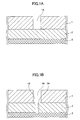
- FIGS. 1A and 1B are diagrams schematically showing that a substrate 1 and a substrate 2 that have been bonded are cut by dicing.
- FIG. 1A shows that the substrate 1 is cut by dicing from the bonded substrate 1 and substrate 2 placed on a dicing tape 3. An opening portion 1A is formed in the substrate 1.
- FIG. 1B shows that the substrate 2 is cut using a blade differing from the step of FIG. 1A and an opening portion 2A is formed when materials of the substrate 2 are different from those of the substrate 1.
- a structure in which the substrate 1 and the substrate 2 are bonded is cut and individualized.
- the corner 1B is likely to be fractured from chipping in some cases. Further, when chipping is generated in a semiconductor device, a crack or failure resulting from the chipping may be generated, so that reliability of the semiconductor device is reduced in some cases.
- Patent Document 2 Japanese Laid-Open Patent Application No. 2001-345289 discloses a method for individualizing semiconductor devices through cleavage.
- FIGS. 1A and 1B no resolution is disclosed regarding the problems of the cases where the structure in which different materials are bonded is individualized.
- a more specific object of the present invention is to provide a method for manufacturing a semiconductor device that can prevent the generation of chipping upon cutting substrates and achieve preferable reliability.
- a method for manufacturing a semiconductor device having a structure where a semiconductor element is mounted on a first substrate the method being characterized by the steps of: bonding the first substrate on which the semiconductor element is mounted and a second substrate made of a material different from a material of the first substrate so as to encapsulate the semiconductor element; forming a first groove in the first substrate and a second groove in the second substrate; and cleaving a portion between the first groove and the second groove so as to individualize the semiconductor device.
- the semiconductor element is made of an optical functional element in order to perform light emission or light reception using the semiconductor element.
- the second substrate is made of an optically transparent material in order to readily perform the light emission or the light reception using the semiconductor element.
- the first substrate and the second substrate are bonded by anodic bonding in order to encapsulate the semiconductor element in a clean manner.
- the above-mentioned method further includes the step of forming through-hole wiring so as to penetrate the first substrate and the semiconductor element is mounted so as to be connected to the through-hole wiring.
- the semiconductor element it is readily possible to connect the semiconductor element to a connection object of the semiconductor element.
- a concave portion on which the semiconductor element is mounted is formed on the first substrate and the semiconductor element is encapsulated by bonding a periphery of the concave portion to the second substrate.
- the semiconductor element is encapsulated by bonding a periphery of the concave portion to the second substrate.
- a method for manufacturing a semiconductor device having a structure where a semiconductor element is mounted on a first substrate is characterized by the steps of: bonding the first substrate on which the semiconductor element is mounted and a second substrate made of a material different from a material of the first substrate so as to encapsulate the semiconductor element; forming a first groove in the first substrate and a second groove in the second substrate; and cleaving a portion between the first groove and the second groove so as to individualize the semiconductor device.
- a first groove is formed on the first substrate, a second groove is formed on the second substrate, and then a portion between the first groove and the second groove is cleaved.
- the method for manufacturing a semiconductor device according to the present invention is capable of manufacturing various types of semiconductor devices.
- an example of an embodiment of the present invention is described with reference to the drawings.
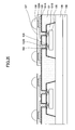
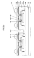
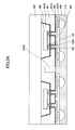
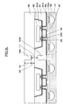
- FIGS. 2A to 2H are diagrams showing a procedure of the method for manufacturing a semiconductor device according to example 1 of the present invention.
- the same reference numerals are assigned to elements described in preceding drawings and description thereof is omitted in some cases.
- a substrate (a first substrate) 101 made of Si is prepared, for example.
- the substrate 101 may be ground so as to have a predetermined thickness (about 200 ⁇ m, for example) as appropriate.
- a step shown in FIG. 2B there are formed plural concave portions 101B for mounting (encapsulating) a semiconductor element in a later step and plural via holes 101C for penetrating each bottom of the plural concave portions 101B.
- a mask made of patterned resist is formed on the substrate 101, and then the concave portions 101B and the via holes 101C are formed by RIE (reactive ion etching), for example.
- an insulating film 101A made of a silicon oxide film is formed by oxidizing a surface of the substrate 101 including an inner wall surface of the via hole 101C.
- the oxide film 101A on a bonding surface 101a on the periphery of the concave portion, to which other substrate (glass) is bonded in a later step is removed by abrasion or the like.
- the oxide film on the bonding surface 101a may be removed in a later step.
- connection layer 102A made of Ni/Au refers to a layer in which a Au layer and a Ni layer are laminated such that the Au layer is formed on a surface (a connection surface) of the connection layer 102A.
- a seed layer (a power supply layer not shown in the drawings) is formed on a surface of the insulating film 101A, and then the via plug 102 and the connection layer 102A are formed on the seed layer by electrolytic plating, for example. Thereafter, the residual seed layer is removed by etching.
- pattern wiring 103 to be connected to the via plug 102 on a rear face of the substrate 101 (an opposite side of where the connection layer 102A is formed).
- a seed layer (not shown in the drawings) is formed on the surface of the insulating film 101A, and a resist pattern (not shown in the drawings) made through patterning is formed on the seed layer by photolithography. Thereafter, the pattern wiring 103 is formed by electrolytic plating using the resist pattern as a mask and the resist pattern is removed. Then, the seed layer exposed resulting from the removal of the resist pattern is removed by etching.
- solder resist layer 107 on the rear face of the substrate 101 such that a portion of the pattern wiring 103 is exposed.
- a connection layer 103A made of Ni/Au is formed on the exposed pattern wiring 103 by nonelectrolytic plating, for example.
- a semiconductor element 105 made of an optical functional element is flip-chip mounted on each of the plurally formed concave portions 101B such that the semiconductor element 105 is connected to the via plug 102 via the bump 104 (the connection layer 102A).
- connection pads made of Au or A1, for example, and formed on the semiconductor element 105 are bonded to the bumps 104 by ultrasonic waves.
- Examples of the optical functional element mounted as the semiconductor element 105 include a light-emitting element and a light-receiving element (a photoelectric conversion element).
- a light-emitting element a light-receiving element
- a photoelectric conversion element a light-receiving element
- an LED is used as the light-emitting element, for example, so as to reduce electric power consumption.
- a substrate (a second substrate) 106 made of an optically transparent material such as glass is bonded.
- the material of the substrate 106 is different from that of the substrate 101.
- the bonding surface 101a on the periphery of the above-mentioned concave portion 101B and the substrate 106 are bonded by anodic bonding, for example.
- the semiconductor element 105 is encapsulated in each of plural spaces (the concave portions 101B) demarcated using the substrate 101 and the substrate 106, so that plural semiconductor devices are formed.
- the substrate 106 is preferably made of an optically transparent material.
- solder ball 108 is formed on the connection layer 103A as appropriate, the forming of the solder ball 108 may be omitted.
- the bonded substrate 101 and substrate 106 made of different materials are cut and semiconductor devices are individualized.
- a dicing tape 109 (made of an adhesive resin material) is attached to an outer surface of the substrate 106 (an opposite side of where the substrate 101 is bonded).
- a groove (cutting) 101D with a depth D1 is formed by dicing from an outer surface of the substrate 101 (an opposite side of where the substrate 106 is bonded).
- the depth D1 is made to be about 150 ⁇ m, for example, and a thickness D2 of the substrate 101 without the groove 101D is made to be about 50 ⁇ m.
- the dicing tape 109 is removed.
- a dicing tape 110 is attached to an outer surface of the substrate 101.
- a groove (cutting) 106A with a depth D3 is formed by dicing from the outer surface of the substrate 106 (the opposite side of where the substrate 101 is bonded).
- the depth D3 is made to be about 150 ⁇ m, for example, and a thickness D4 of the substrate 106 without the groove 106A is made to be about 50 ⁇ m.
- a connection portion 111 made of the substrate 101 with the thickness of 50 ⁇ m and the substrate 106 with the thickness of 50 ⁇ m is formed between the groove 101D and the groove 106A.
- the dicing tape 110 is stretched by pulling or stress is applied to the substrate 106 (the substrate 101) using a rubber roller, for example.
- the connection portion 111 (the substrate 101 and the substrate 106) formed between the groove 101D and the groove 106A is cut through cleavage and semiconductor devices 100 are individualized.
- the individualized semiconductor devices 100 are removed from the dicing tape 110 using a unit such as a die picker. In this manner, it is possible to form the semiconductor devices 100 according to the present invention.
- the method for manufacturing a semiconductor device in the present example it is possible to prevent the generation of chipping that has been problematic in cutting by conventional dicing. And it is possible to prevent the generation of a crack or failure of a semiconductor device resulting from the chipping. Thus, it is possible to manufacture a semiconductor device with preferable reliability.
- a substrate made of an optically transparent material such as glass
- a material suitable for mounting such as Si is used for the substrate on which the semiconductor device is mounted, the substrate being bonded to the substrate made of the optically transparent material.
- the semiconductor device according to the present example has the structure where the substrates made of different materials are bonded and it is necessary to individualize such a structure.
- the first groove (the groove 101D) is formed on the first substrate and the second groove (the groove 106A) is formed on the second substrate. Then, the portion between the first groove and the second groove (the connection portion 111) is cleaved, so that the first substrate and the second substrate are cut.
- the generation of a difference in level resulting from a change of dicing blades is eliminated on a cut surface resulting from the cutting.
- the cut surface from cleavage is less likely to have protrusion or concavity and convexity formed thereon.
- a shape of the cut surface is preferable and chipping is less likely to be generated.
- the substrate 101 made of Si and the substrate 106 made of glass are used, so that it is possible to bond the substrate 101 and the substrate 106 by anodic bonding.
- the via plug 102 connected to the semiconductor element 105 and penetrating the substrate 101 is formed before the semiconductor element 105 is mounted, so that it is possible to manufacture a semiconductor device which readily enables connection between the semiconductor element 105 and a connection object (boards and the like).
- materials constituting the semiconductor device 100 according to the present example are not limited to the above-mentioned case and it is possible to form the semiconductor device 100 using various types of materials.
- the present invention it is possible provide a method for manufacturing a semiconductor device in which the generation of chipping when cutting substrates is prevented and a semiconductor device with preferable reliability is manufactured.
Landscapes
- Engineering & Computer Science (AREA)
- Microelectronics & Electronic Packaging (AREA)
- Computer Hardware Design (AREA)
- Dicing (AREA)
- Led Device Packages (AREA)
Abstract
Description
- The present invention relates to a method for manufacturing a semiconductor device in which a light-emitting element is mounted on a substrate.
- Upon manufacturing a semiconductor device in which a semiconductor element is mounted on a substrate, for example, a method for forming plural semiconductor devices is employed in some cases. In such cases, plural semiconductor elements are mounted on a substrate, the substrate is cut and the plural semiconductor elements are individualized, so that plural semiconductor devices are formed. Generally, the substrate is cut (individualization) by dicing, for example (refer to Patent Document 1). Dicing is a method for cutting a substrate using a blade rotating at a high speed.
- Patent Document 1:
Japanese Laid-Open Patent Application No. 2005-129643 - Patent Document 2:
Japanese Laid-Open Patent Application No. 2001-345289 - However, when the substrate is cut by dicing, a fracture referred to as chipping may be generated in the substrate since the blade rotating at a high speed is used. This is problematic in that reliability of semiconductor devices is reduced.
- In particular, when cutting a structure in which plural substrates are bonded, it is necessary to use different blades for different materials depending on the materials of the substrates in some cases. In accordance with this, a difference in level is generated in a cut surface, so that chipping is likely to be generated in some cases.
- For example, FIGS. 1A and 1B are diagrams schematically showing that a
substrate 1 and asubstrate 2 that have been bonded are cut by dicing. - First, FIG. 1A shows that the
substrate 1 is cut by dicing from thebonded substrate 1 andsubstrate 2 placed on adicing tape 3. Anopening portion 1A is formed in thesubstrate 1. - Next, FIG. 1B shows that the
substrate 2 is cut using a blade differing from the step of FIG. 1A and anopening portion 2A is formed when materials of thesubstrate 2 are different from those of thesubstrate 1. In this case, a structure in which thesubstrate 1 and thesubstrate 2 are bonded is cut and individualized. However, in a step shown in FIG. 1B, it is necessary to use a blade smaller than a width of theopening portion 1A, so that acorner 1B is formed on a bottom of theopening portion 1A. - In accordance with this, the
corner 1B is likely to be fractured from chipping in some cases. Further, when chipping is generated in a semiconductor device, a crack or failure resulting from the chipping may be generated, so that reliability of the semiconductor device is reduced in some cases. - The above-mentioned Patent Document 2 (
Japanese Laid-Open Patent Application No. 2001-345289 - It is a general object of the present invention to provide an improved and useful method for manufacturing a semiconductor device in which the above-mentioned problems are eliminated.
- A more specific object of the present invention is to provide a method for manufacturing a semiconductor device that can prevent the generation of chipping upon cutting substrates and achieve preferable reliability.
- According to the present invention, there is provided a method for manufacturing a semiconductor device having a structure where a semiconductor element is mounted on a first substrate, the method being characterized by the steps of: bonding the first substrate on which the semiconductor element is mounted and a second substrate made of a material different from a material of the first substrate so as to encapsulate the semiconductor element; forming a first groove in the first substrate and a second groove in the second substrate; and cleaving a portion between the first groove and the second groove so as to individualize the semiconductor device.
- According to the above-mentioned method for manufacturing a semiconductor device, it is possible to prevent the generation of chipping when cutting substrates and to manufacture a semiconductor device with preferable reliability.
- Preferably, the semiconductor element is made of an optical functional element in order to perform light emission or light reception using the semiconductor element.
- Preferably, the second substrate is made of an optically transparent material in order to readily perform the light emission or the light reception using the semiconductor element.
- Preferably, the first substrate and the second substrate are bonded by anodic bonding in order to encapsulate the semiconductor element in a clean manner.
- Preferably, the above-mentioned method further includes the step of forming through-hole wiring so as to penetrate the first substrate and the semiconductor element is mounted so as to be connected to the through-hole wiring. In accordance with this, it is readily possible to connect the semiconductor element to a connection object of the semiconductor element.
- Preferably, a concave portion on which the semiconductor element is mounted is formed on the first substrate and the semiconductor element is encapsulated by bonding a periphery of the concave portion to the second substrate. In accordance with this, it is readily possible to encapsulate the semiconductor device.
- According to the present invention, it is possible to prevent the generation of chipping upon cutting substrates and to manufacture a semiconductor device with preferable reliability.
- Other objects, features and advantage of the present invention will become more apparent from the following detailed description when read in conjunction with the accompanying drawings.
-
- FIG. 1A is a (first) diagram showing a conventional method for cutting substrates;
- FIG. 1B is a (second) diagram showing a conventional method for cutting substrates;
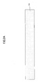
- FIG. 2A is a (first) diagram showing a method for manufacturing a semiconductor device according to example 1 of the present invention;
- FIG. 2B is a (second) diagram showing a method for manufacturing a semiconductor device according to example 1 of the present invention;
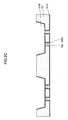
- FIG. 2C is a (third) diagram showing a method for manufacturing a semiconductor device according to example 1 of the present invention;
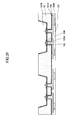
- FIG. 2D is a (fourth) diagram showing a method for manufacturing a semiconductor device according to example 1 of the present invention;
- FIG. 2E is a (fifth) diagram showing a method for manufacturing a semiconductor device according to example 1 of the present invention;
- FIG. 2F is a (sixth) diagram showing a method for manufacturing a semiconductor device according to example 1 of the present invention;
- FIG. 2G is a (seventh) diagram showing a method for manufacturing a semiconductor device according to example 1 of the present invention;
- FIG. 2H is an (eighth) diagram showing a method for manufacturing a semiconductor device according to example 1 of the present invention;
- FIG. 2I is a (ninth) diagram showing a method for manufacturing a semiconductor device according to example 1 of the present invention;
- FIG. 2J is a (tenth) diagram showing a method for manufacturing a semiconductor device according to example 1 of the present invention;
- FIG. 2K is an (eleventh) diagram showing a method for manufacturing a semiconductor device according to example 1 of the present invention;
- FIG. 2L is a (twelfth) diagram showing a method for manufacturing a semiconductor device according to example 1 of the present invention;
- FIG. 2M is a (thirteen) diagram showing a method for manufacturing a semiconductor device according to example 1 of the present invention; and
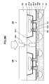
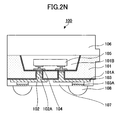
- FIG. 2N is a (fourteen) diagram showing a method for manufacturing a semiconductor device according to example 1 of the present invention.
- In the following, embodiments of the present invention will be described with reference to the accompanying drawings.
- According to the present invention, a method for manufacturing a semiconductor device having a structure where a semiconductor element is mounted on a first substrate is characterized by the steps of: bonding the first substrate on which the semiconductor element is mounted and a second substrate made of a material different from a material of the first substrate so as to encapsulate the semiconductor element; forming a first groove in the first substrate and a second groove in the second substrate; and cleaving a portion between the first groove and the second groove so as to individualize the semiconductor device.
- Conventionally, when a substrate is cut, dicing using a blade rotating at a high speed is generally employed, so that chipping is likely to be generated in the substrate. In particular, in a structure in which substrates made of different materials are bonded, it is necessary to use different blades in some cases. As a result, chipping is more likely to be generated, so that reliability of a semiconductor device may be reduced in some cases.
- By contrast, in the method for manufacturing a semiconductor device according to the present invention, when a structure in which a first substrate and a second substrate made of different materials are bonded is individualized, a first groove is formed on the first substrate, a second groove is formed on the second substrate, and then a portion between the first groove and the second groove is cleaved.
- In accordance with this, it is possible to prevent the generation of chipping on the substrates and to prevent the generation of a crack or failure resulting from the chipping. Thus, it is possible to manufacture a semiconductor device with preferable reliability.
- The method for manufacturing a semiconductor device according to the present invention is capable of manufacturing various types of semiconductor devices. In the following, an example of an embodiment of the present invention is described with reference to the drawings.
- FIGS. 2A to 2H are diagrams showing a procedure of the method for manufacturing a semiconductor device according to example 1 of the present invention. The same reference numerals are assigned to elements described in preceding drawings and description thereof is omitted in some cases.
- First, in a step shown in FIG. 2A, a substrate (a first substrate) 101 made of Si is prepared, for example. In addition, the
substrate 101 may be ground so as to have a predetermined thickness (about 200 µm, for example) as appropriate. - Next, in a step shown in FIG. 2B, there are formed plural
concave portions 101B for mounting (encapsulating) a semiconductor element in a later step and plural viaholes 101C for penetrating each bottom of the pluralconcave portions 101B. Upon forming theconcave portions 101B and the via holes 101C, a mask made of patterned resist is formed on thesubstrate 101, and then theconcave portions 101B and the via holes 101C are formed by RIE (reactive ion etching), for example. Further, an insulatingfilm 101A made of a silicon oxide film is formed by oxidizing a surface of thesubstrate 101 including an inner wall surface of the viahole 101C. Preferably, theoxide film 101A on abonding surface 101a on the periphery of the concave portion, to which other substrate (glass) is bonded in a later step is removed by abrasion or the like. Moreover, the oxide film on thebonding surface 101a may be removed in a later step. - Next, in a step shown in FIG. 2C, there are formed a via plug 102 (made of Cu) in the via
hole 101C and aconnection layer 102A made of a Ni/Au layer on the viaplug 102 through a plating method, for example. Theconnection layer 102A made of Ni/Au refers to a layer in which a Au layer and a Ni layer are laminated such that the Au layer is formed on a surface (a connection surface) of theconnection layer 102A. In the afore-mentioned plating method, a seed layer (a power supply layer not shown in the drawings) is formed on a surface of the insulatingfilm 101A, and then the viaplug 102 and theconnection layer 102A are formed on the seed layer by electrolytic plating, for example. Thereafter, the residual seed layer is removed by etching. - Next, in a step shown in FIG. 2D, there is formed
pattern wiring 103 to be connected to the viaplug 102 on a rear face of the substrate 101 (an opposite side of where theconnection layer 102A is formed). - Upon forming the
pattern wiring 103, first, a seed layer (not shown in the drawings) is formed on the surface of the insulatingfilm 101A, and a resist pattern (not shown in the drawings) made through patterning is formed on the seed layer by photolithography. Thereafter, thepattern wiring 103 is formed by electrolytic plating using the resist pattern as a mask and the resist pattern is removed. Then, the seed layer exposed resulting from the removal of the resist pattern is removed by etching. - Next, in a step shown in FIG. 2E, there is formed a solder resist
layer 107 on the rear face of thesubstrate 101 such that a portion of thepattern wiring 103 is exposed. Then, aconnection layer 103A made of Ni/Au is formed on the exposedpattern wiring 103 by nonelectrolytic plating, for example. - Next, in a step shown in FIG. 2F, a
bump 104 made of a Au bonding wire by wire bonding method, for example, is disposed on theconnection layer 102A. - Next, in a step shown in FIG. 2G, a
semiconductor element 105 made of an optical functional element is flip-chip mounted on each of the plurally formedconcave portions 101B such that thesemiconductor element 105 is connected to the viaplug 102 via the bump 104 (theconnection layer 102A). In this case, connection pads made of Au or A1, for example, and formed on thesemiconductor element 105 are bonded to thebumps 104 by ultrasonic waves. - Examples of the optical functional element mounted as the
semiconductor element 105 include a light-emitting element and a light-receiving element (a photoelectric conversion element). Preferably, an LED is used as the light-emitting element, for example, so as to reduce electric power consumption. - Next, in a step shown in FIG. 2H, a substrate (a second substrate) 106 made of an optically transparent material such as glass is bonded. The material of the
substrate 106 is different from that of thesubstrate 101. In this case, thebonding surface 101a on the periphery of the above-mentionedconcave portion 101B and thesubstrate 106 are bonded by anodic bonding, for example. In this manner, thesemiconductor element 105 is encapsulated in each of plural spaces (theconcave portions 101B) demarcated using thesubstrate 101 and thesubstrate 106, so that plural semiconductor devices are formed. Further, when thesemiconductor element 105 is made of an optical functional element such as a light-emitting element, thesubstrate 106 is preferably made of an optically transparent material. - In addition, although a
solder ball 108 is formed on theconnection layer 103A as appropriate, the forming of thesolder ball 108 may be omitted. - In steps shown in FIGS. 2I to 2N, the bonded
substrate 101 andsubstrate 106 made of different materials are cut and semiconductor devices are individualized. - First, in a step shown in FIG. 2I, a dicing tape 109 (made of an adhesive resin material) is attached to an outer surface of the substrate 106 (an opposite side of where the
substrate 101 is bonded). - Next, in a step shown in FIG. 2J, a groove (cutting) 101D with a depth D1 is formed by dicing from an outer surface of the substrate 101 (an opposite side of where the
substrate 106 is bonded). In this case, when a thickness of thesubstrate 101 is assumed to be 200 µm, the depth D1 is made to be about 150 µm, for example, and a thickness D2 of thesubstrate 101 without thegroove 101D is made to be about 50 µm. Thereafter, the dicingtape 109 is removed. - Next, in a step shown in FIG. 2K, a dicing
tape 110 is attached to an outer surface of thesubstrate 101. - Next, in a step shown in FIG. 2L, a groove (cutting) 106A with a depth D3 is formed by dicing from the outer surface of the substrate 106 (the opposite side of where the
substrate 101 is bonded). In this case, when a thickness of thesubstrate 106 is assumed to be 200 µm, the depth D3 is made to be about 150 µm, for example, and a thickness D4 of thesubstrate 106 without thegroove 106A is made to be about 50 µm. In other words, aconnection portion 111 made of thesubstrate 101 with the thickness of 50 µm and thesubstrate 106 with the thickness of 50 µm is formed between thegroove 101D and thegroove 106A. - Next, in a step shown in FIG. 2M, the dicing
tape 110 is stretched by pulling or stress is applied to the substrate 106 (the substrate 101) using a rubber roller, for example. In accordance with this, the connection portion 111 (thesubstrate 101 and the substrate 106) formed between thegroove 101D and thegroove 106A is cut through cleavage andsemiconductor devices 100 are individualized. - Next, in a step shown in FIG. 2N, the
individualized semiconductor devices 100 are removed from the dicingtape 110 using a unit such as a die picker. In this manner, it is possible to form thesemiconductor devices 100 according to the present invention. - According to the method for manufacturing a semiconductor device in the present example, it is possible to prevent the generation of chipping that has been problematic in cutting by conventional dicing. And it is possible to prevent the generation of a crack or failure of a semiconductor device resulting from the chipping. Thus, it is possible to manufacture a semiconductor device with preferable reliability.
- In particular, in a structure in which substrates made of different materials are bonded, conventional individualization methods require different blades in some cases. In accordance with this, chipping is more likely to be generated, so that reliability of a semiconductor device may be reduced in some cases.
- For example, when the semiconductor element made of an optical functional element is encapsulated as in the semiconductor device according to the present example, preferably, a substrate made of an optically transparent material such as glass is used. Further, preferably, a material suitable for mounting such as Si is used for the substrate on which the semiconductor device is mounted, the substrate being bonded to the substrate made of the optically transparent material.
- In this manner, preferably, the semiconductor device according to the present example has the structure where the substrates made of different materials are bonded and it is necessary to individualize such a structure. In view of this, in the present example, when individualizing the structure where the first substrate (the substrate 101) and the second substrate (the substrate 106) made of different materials are bonded, the first groove (the
groove 101D) is formed on the first substrate and the second groove (thegroove 106A) is formed on the second substrate. Then, the portion between the first groove and the second groove (the connection portion 111) is cleaved, so that the first substrate and the second substrate are cut. - In accordance with this, the generation of a difference in level resulting from a change of dicing blades (blade width, for example) is eliminated on a cut surface resulting from the cutting. Moreover, the cut surface from cleavage is less likely to have protrusion or concavity and convexity formed thereon. A shape of the cut surface is preferable and chipping is less likely to be generated. Thus, it is possible to prevent the generation of a crack or failure and to manufacture a semiconductor device with preferable reliability.
- Further, in the present example, when the mounted
semiconductor element 105 is encapsulated, thesubstrate 101 made of Si and thesubstrate 106 made of glass are used, so that it is possible to bond thesubstrate 101 and thesubstrate 106 by anodic bonding. In accordance with this, it is possible to maintain a space where thesemiconductor element 105 is encapsulated in a clean manner in comparison with a case where substrates are bonded using bond such as resin. And it is possible to maintain properties of the semiconductor element (optical functional element) 105 in a preferable manner. - Moreover, in the present example, the via
plug 102 connected to thesemiconductor element 105 and penetrating thesubstrate 101 is formed before thesemiconductor element 105 is mounted, so that it is possible to manufacture a semiconductor device which readily enables connection between thesemiconductor element 105 and a connection object (boards and the like). - Further, materials constituting the
semiconductor device 100 according to the present example are not limited to the above-mentioned case and it is possible to form thesemiconductor device 100 using various types of materials. - According to the present invention, it is possible provide a method for manufacturing a semiconductor device in which the generation of chipping when cutting substrates is prevented and a semiconductor device with preferable reliability is manufactured.
- The present invention is not limited to the specifically disclosed embodiment, and variations and modifications may be made without departing from the scope of the present invention.
Claims (6)
- A method for manufacturing a semiconductor device having a structure where a semiconductor element is mounted on a first substrate, the method being characterized by the steps of:bonding the first substrate on which the semiconductor element is mounted and a second substrate made of a material different from a material of the first substrate so as to encapsulate the semiconductor element;forming a first groove in the first substrate and a second groove in the second substrate; andcleaving a portion between the first groove and the second groove so as to individualize the semiconductor device.
- The method for manufacturing a semiconductor device according to claim 1, wherein
the semiconductor element is made of an optical functional element. - The method for manufacturing a semiconductor device according to claim 2, wherein
the second substrate is made of an optically transparent material. - The method for manufacturing a semiconductor device according to any one of claims 1 to 3, wherein
the first substrate and the second substrate are bonded by anodic bonding. - The method for manufacturing a semiconductor device according to any one of claims 1 to 4, being further characterized by the step of:forming through-hole wiring so as to penetrate the first substrate, whereinthe semiconductor element is mounted so as to be connected to the through-hole wiring.
- The method for manufacturing a semiconductor device according to any one of claims 1 to 5, wherein
a concave portion on which the semiconductor element is mounted is formed on the first substrate and the semiconductor element is encapsulated by bonding a periphery of the concave portion to the second substrate.
Applications Claiming Priority (1)
| Application Number | Priority Date | Filing Date | Title |
|---|---|---|---|
| JP2006001802A JP2007184426A (en) | 2006-01-06 | 2006-01-06 | Manufacturing method of semiconductor device |
Publications (3)
| Publication Number | Publication Date |
|---|---|
| EP1806782A2 true EP1806782A2 (en) | 2007-07-11 |
| EP1806782A3 EP1806782A3 (en) | 2010-03-03 |
| EP1806782B1 EP1806782B1 (en) | 2011-08-10 |
Family
ID=37876964
Family Applications (1)
| Application Number | Title | Priority Date | Filing Date |
|---|---|---|---|
| EP06256362A Not-in-force EP1806782B1 (en) | 2006-01-06 | 2006-12-14 | Method for manufacturing semiconductor device |
Country Status (5)
| Country | Link |
|---|---|
| US (1) | US7494898B2 (en) |
| EP (1) | EP1806782B1 (en) |
| JP (1) | JP2007184426A (en) |
| KR (1) | KR20070074460A (en) |
| TW (1) | TW200807751A (en) |
Cited By (4)
| Publication number | Priority date | Publication date | Assignee | Title |
|---|---|---|---|---|
| WO2009103283A1 (en) * | 2008-02-22 | 2009-08-27 | Osram Opto Semiconductors Gmbh | Method for producing a plurality of radiation emitting components and radiation emitting component |
| WO2015184245A1 (en) * | 2014-05-30 | 2015-12-03 | Cree, Inc. | Submount based light emitter components and methods |
| EP2058858B1 (en) * | 2007-10-26 | 2018-12-05 | Shinko Electric Industries Co., Ltd. | Silicon interposer and semiconductor device package and semiconductor device incorporating the same and interposer manufacture |
| US10957736B2 (en) | 2018-03-12 | 2021-03-23 | Cree, Inc. | Light emitting diode (LED) components and methods |
Families Citing this family (33)
| Publication number | Priority date | Publication date | Assignee | Title |
|---|---|---|---|---|
| JP2007184426A (en) * | 2006-01-06 | 2007-07-19 | Shinko Electric Ind Co Ltd | Manufacturing method of semiconductor device |
| US9780268B2 (en) | 2006-04-04 | 2017-10-03 | Cree, Inc. | Submount based surface mount device (SMD) light emitter components and methods |
| TW200843135A (en) * | 2007-04-23 | 2008-11-01 | Augux Co Ltd | Method of packaging light emitting diode with high heat-dissipating efficiency and the structure thereof |
| JP4809308B2 (en) * | 2007-09-21 | 2011-11-09 | 新光電気工業株式会社 | Substrate manufacturing method |
| JP5108579B2 (en) * | 2008-03-21 | 2012-12-26 | シチズンファインテックミヨタ株式会社 | Electronic component package manufacturing method and electronic component package |
| KR100992778B1 (en) | 2008-05-23 | 2010-11-05 | 엘지이노텍 주식회사 | Light emitting device package and method for manufacturing the same |
| US20100176507A1 (en) * | 2009-01-14 | 2010-07-15 | Hymite A/S | Semiconductor-based submount with electrically conductive feed-throughs |
| KR101064026B1 (en) * | 2009-02-17 | 2011-09-08 | 엘지이노텍 주식회사 | Light emitting device package and manufacturing method thereof |
| US8609512B2 (en) * | 2009-03-27 | 2013-12-17 | Electro Scientific Industries, Inc. | Method for laser singulation of chip scale packages on glass substrates |
| US7892950B2 (en) * | 2009-04-29 | 2011-02-22 | Freescale Semiconductor, Inc. | Methodology for processing a panel during semiconductor device fabrication |
| JP2011040621A (en) * | 2009-08-12 | 2011-02-24 | Renesas Electronics Corp | Method of designing semiconductor device, and method of manufacturing the same |
| JP2011222623A (en) * | 2010-04-06 | 2011-11-04 | Disco Abrasive Syst Ltd | Method for processing optical device wafer |
| JP2012186309A (en) * | 2011-03-04 | 2012-09-27 | Omron Corp | Manufacturing method of wafer level package, and wafer level package |
| US10222032B2 (en) | 2012-03-30 | 2019-03-05 | Cree, Inc. | Light emitter components and methods having improved electrical contacts |
| US9735198B2 (en) | 2012-03-30 | 2017-08-15 | Cree, Inc. | Substrate based light emitter devices, components, and related methods |
| US10134961B2 (en) | 2012-03-30 | 2018-11-20 | Cree, Inc. | Submount based surface mount device (SMD) light emitter components and methods |
| KR101524046B1 (en) * | 2013-11-21 | 2015-06-01 | 주식회사 루멘스 | Light emitting device package, backlight unit, illumination device and its manufacturing method |
| US9831407B2 (en) | 2013-11-21 | 2017-11-28 | Lumens Co., Ltd. | Light emitting device package, backlight unit, illumination apparatus, and method of manufacturing light emitting device package |
| KR101524044B1 (en) * | 2013-11-21 | 2015-06-02 | 주식회사 루멘스 | Light emitting device package, backlight unit and illumination device |
| CN104752584A (en) * | 2013-12-25 | 2015-07-01 | 苏州矩阵光电有限公司 | LED packaging structure |
| US9196592B2 (en) | 2014-01-10 | 2015-11-24 | International Business Machines Corporation | Methods of managing metal density in dicing channel and related integrated circuit structures |
| CN103822143A (en) * | 2014-02-18 | 2014-05-28 | 江苏新广联绿色照明工程有限公司 | LED (light emitting diode) street lamp light source module with silicon substrates |
| CN103887238A (en) * | 2014-04-01 | 2014-06-25 | 惠州硕贝德无线科技股份有限公司 | Cutting and classifying method for wafer after BGA package is completed |
| US12294042B2 (en) | 2015-03-31 | 2025-05-06 | Creeled, Inc. | Light emitting diodes and methods with encapsulation |
| US12364074B2 (en) | 2015-03-31 | 2025-07-15 | Creeled, Inc. | Light emitting diodes and methods |
| JP2018060988A (en) * | 2016-10-04 | 2018-04-12 | 日本特殊陶業株式会社 | Lid member, light-emitting device, and manufacturing method therefor |
| JP6866664B2 (en) * | 2017-02-06 | 2021-04-28 | 日亜化学工業株式会社 | Manufacturing method of light emitting device |
| US10347806B2 (en) * | 2017-04-12 | 2019-07-09 | Luminus, Inc. | Packaged UV-LED device with anodic bonded silica lens and no UV-degradable adhesive |
| US10672957B2 (en) | 2017-07-19 | 2020-06-02 | Cree, Inc. | LED apparatuses and methods for high lumen output density |
| EP3439050B1 (en) * | 2017-08-02 | 2020-10-28 | Lg Innotek Co. Ltd | Light emitting device package |
| KR102684757B1 (en) * | 2019-08-22 | 2024-07-16 | 삼성디스플레이 주식회사 | Display device |
| DE102020107409B4 (en) * | 2020-03-18 | 2023-11-02 | OSRAM Opto Semiconductors Gesellschaft mit beschränkter Haftung | HOUSING FOR AN OPTOELECTRONIC SEMICONDUCTOR COMPONENT AND OPTOELECTRONIC SEMICONDUCTOR COMPONENT |
| DE102024202118A1 (en) * | 2024-03-07 | 2025-09-11 | Robert Bosch Gesellschaft mit beschränkter Haftung | Process for the production and separation of MEMS components |
Family Cites Families (30)
| Publication number | Priority date | Publication date | Assignee | Title |
|---|---|---|---|---|
| JPH0611071B2 (en) * | 1983-09-07 | 1994-02-09 | 三洋電機株式会社 | Method for dividing compound semiconductor substrate |
| JPH10261808A (en) * | 1997-01-17 | 1998-09-29 | Hitachi Cable Ltd | Plastic circuit molded product for mounting photosensor element and method for manufacturing photosensor |
| TW456004B (en) * | 1998-02-10 | 2001-09-21 | Nissha Printing | Substrate sheet for semiconductor module, method and apparatus for manufacturing the same |
| US6413839B1 (en) * | 1998-10-23 | 2002-07-02 | Emcore Corporation | Semiconductor device separation using a patterned laser projection |
| US20050263854A1 (en) * | 1998-10-23 | 2005-12-01 | Shelton Bryan S | Thick laser-scribed GaN-on-sapphire optoelectronic devices |
| JP2001345289A (en) | 2000-05-31 | 2001-12-14 | Nec Corp | Method for manufacturing semiconductor device |
| JP3616872B2 (en) * | 2000-09-14 | 2005-02-02 | 住友電気工業株式会社 | Diamond wafer chip making method |
| US7307775B2 (en) * | 2000-12-07 | 2007-12-11 | Texas Instruments Incorporated | Methods for depositing, releasing and packaging micro-electromechanical devices on wafer substrates |
| US6744072B2 (en) * | 2001-10-02 | 2004-06-01 | Xerox Corporation | Substrates having increased thermal conductivity for semiconductor structures |
| US6962834B2 (en) * | 2002-03-22 | 2005-11-08 | Stark David H | Wafer-level hermetic micro-device packages |
| US6960813B2 (en) * | 2002-06-10 | 2005-11-01 | New Wave Research | Method and apparatus for cutting devices from substrates |
| US6806544B2 (en) * | 2002-11-05 | 2004-10-19 | New Wave Research | Method and apparatus for cutting devices from conductive substrates secured during cutting by vacuum pressure |
| US6580054B1 (en) * | 2002-06-10 | 2003-06-17 | New Wave Research | Scribing sapphire substrates with a solid state UV laser |
| JP4271904B2 (en) * | 2002-06-24 | 2009-06-03 | 富士フイルム株式会社 | Method for manufacturing solid-state imaging device |
| US6995032B2 (en) * | 2002-07-19 | 2006-02-07 | Cree, Inc. | Trench cut light emitting diodes and methods of fabricating same |
| US6982470B2 (en) * | 2002-11-27 | 2006-01-03 | Seiko Epson Corporation | Semiconductor device, method of manufacturing the same, cover for semiconductor device, and electronic equipment |
| DE60311678T2 (en) * | 2002-12-20 | 2007-11-22 | Cree, Inc. | METHOD FOR PRODUCING SEMICONDUCTOR DEVICES WITH MESASTRUCTURES AND MULTIPLE PASSIVATION LAYERS AND RELATED DEVICES |
| TWI248244B (en) * | 2003-02-19 | 2006-01-21 | J P Sercel Associates Inc | System and method for cutting using a variable astigmatic focal beam spot |
| US6949449B2 (en) * | 2003-07-11 | 2005-09-27 | Electro Scientific Industries, Inc. | Method of forming a scribe line on a ceramic substrate |
| JP4259979B2 (en) * | 2003-10-22 | 2009-04-30 | 新光電気工業株式会社 | Light transmissive cover, device provided with the same, and manufacturing method thereof |
| EP1681717B1 (en) * | 2003-11-07 | 2017-03-29 | Shinko Electric Industries Co., Ltd. | Electronic device |
| US7008861B2 (en) * | 2003-12-11 | 2006-03-07 | Cree, Inc. | Semiconductor substrate assemblies and methods for preparing and dicing the same |
| JP2005260154A (en) * | 2004-03-15 | 2005-09-22 | Tokyo Seimitsu Co Ltd | Method of manufacturing chip |
| US7202141B2 (en) * | 2004-03-29 | 2007-04-10 | J.P. Sercel Associates, Inc. | Method of separating layers of material |
| US7087463B2 (en) * | 2004-08-04 | 2006-08-08 | Gelcore, Llc | Laser separation of encapsulated submount |
| JP2006086516A (en) * | 2004-08-20 | 2006-03-30 | Showa Denko Kk | Manufacturing method of semiconductor light emitting device |
| TWI327340B (en) * | 2004-10-07 | 2010-07-11 | Showa Denko Kk | Production method for semiconductor device |
| US7378288B2 (en) * | 2005-01-11 | 2008-05-27 | Semileds Corporation | Systems and methods for producing light emitting diode array |
| US7306975B2 (en) * | 2005-07-01 | 2007-12-11 | Texas Instruments Incorporated | Semiconductor wafer cutting blade and method |
| JP2007184426A (en) * | 2006-01-06 | 2007-07-19 | Shinko Electric Ind Co Ltd | Manufacturing method of semiconductor device |
-
2006
- 2006-01-06 JP JP2006001802A patent/JP2007184426A/en active Pending
- 2006-12-14 EP EP06256362A patent/EP1806782B1/en not_active Not-in-force
- 2006-12-18 TW TW095147438A patent/TW200807751A/en unknown
- 2006-12-19 US US11/641,336 patent/US7494898B2/en active Active
- 2006-12-20 KR KR1020060131037A patent/KR20070074460A/en not_active Withdrawn
Non-Patent Citations (1)
| Title |
|---|
| None |
Cited By (7)
| Publication number | Priority date | Publication date | Assignee | Title |
|---|---|---|---|---|
| EP2058858B1 (en) * | 2007-10-26 | 2018-12-05 | Shinko Electric Industries Co., Ltd. | Silicon interposer and semiconductor device package and semiconductor device incorporating the same and interposer manufacture |
| WO2009103283A1 (en) * | 2008-02-22 | 2009-08-27 | Osram Opto Semiconductors Gmbh | Method for producing a plurality of radiation emitting components and radiation emitting component |
| DE102008014927A1 (en) * | 2008-02-22 | 2009-08-27 | Osram Opto Semiconductors Gmbh | Method for producing a plurality of radiation-emitting components and radiation-emitting component |
| US8790939B2 (en) | 2008-02-22 | 2014-07-29 | Osram Opto Semiconductors Gmbh | Method for producing a plurality of radiation-emitting components and radiation-emitting component |
| WO2015184245A1 (en) * | 2014-05-30 | 2015-12-03 | Cree, Inc. | Submount based light emitter components and methods |
| US9691949B2 (en) | 2014-05-30 | 2017-06-27 | Cree, Inc. | Submount based light emitter components and methods |
| US10957736B2 (en) | 2018-03-12 | 2021-03-23 | Cree, Inc. | Light emitting diode (LED) components and methods |
Also Published As
| Publication number | Publication date |
|---|---|
| US20070161211A1 (en) | 2007-07-12 |
| JP2007184426A (en) | 2007-07-19 |
| US7494898B2 (en) | 2009-02-24 |
| EP1806782B1 (en) | 2011-08-10 |
| TW200807751A (en) | 2008-02-01 |
| KR20070074460A (en) | 2007-07-12 |
| EP1806782A3 (en) | 2010-03-03 |
Similar Documents
| Publication | Publication Date | Title |
|---|---|---|
| EP1806782B1 (en) | Method for manufacturing semiconductor device | |
| CN1222024C (en) | Method for producing packaged integrated circuit devices & packaged integrated circuit devices produced thereby | |
| JP3880278B2 (en) | Solid-state imaging device and manufacturing method thereof | |
| US8952519B2 (en) | Chip package and fabrication method thereof | |
| JP5148045B2 (en) | Optocoupler and optocoupler manufacturing method | |
| JP5275642B2 (en) | Light emitting device and manufacturing method thereof | |
| JP2009064839A (en) | Optical device and manufacturing method thereof | |
| EP1898462A2 (en) | Semiconductor apparatus | |
| US9105771B2 (en) | Method for producing at least one optoelectronic semiconductor component | |
| US9196571B2 (en) | Chip device packages and fabrication methods thereof | |
| KR20040092435A (en) | Semiconductor device and manufacturing method thereof | |
| JP2008092417A (en) | Semiconductor imaging device, method for manufacturing the same, semiconductor imaging device, and semiconductor imaging module | |
| EP2040288A2 (en) | Method of forming semiconductor chip wiring pattern using alignment marks | |
| US20090095974A1 (en) | Semiconductor package and manufacturing method thereof | |
| EP1418616A1 (en) | Electronic parts packaging structure and method of manufacturing the same | |
| WO2005093829A1 (en) | Semiconductor package having an interfacial adhesive layer | |
| US20130099269A1 (en) | Electronic assembly | |
| JP2008140873A (en) | Flip chip mounted group III-V semiconductor device and method for manufacturing the same | |
| JP4537793B2 (en) | Sensor unit and manufacturing method thereof | |
| JP2002176184A (en) | Infrared data communication module and manufacturing method thereof | |
| US8110447B2 (en) | Method of making and designing lead frames for semiconductor packages | |
| US7681306B2 (en) | Method of forming an assembly to house one or more micro components | |
| JP2004020767A (en) | Photo-electric composite substrate and method of manufacturing the same | |
| KR100868616B1 (en) | Semiconductor flip-chip package component and fabricating method | |
| JP4681648B2 (en) | Resin sealing module, optical module, and resin sealing method |
Legal Events
| Date | Code | Title | Description |
|---|---|---|---|
| PUAI | Public reference made under article 153(3) epc to a published international application that has entered the european phase |
Free format text: ORIGINAL CODE: 0009012 |
|
| AK | Designated contracting states |
Kind code of ref document: A2 Designated state(s): AT BE BG CH CY CZ DE DK EE ES FI FR GB GR HU IE IS IT LI LT LU LV MC NL PL PT RO SE SI SK TR |
|
| AX | Request for extension of the european patent |
Extension state: AL BA HR MK YU |
|
| PUAL | Search report despatched |
Free format text: ORIGINAL CODE: 0009013 |
|
| AK | Designated contracting states |
Kind code of ref document: A3 Designated state(s): AT BE BG CH CY CZ DE DK EE ES FI FR GB GR HU IE IS IT LI LT LU LV MC NL PL PT RO SE SI SK TR |
|
| AX | Request for extension of the european patent |
Extension state: AL BA HR MK RS |
|
| RIC1 | Information provided on ipc code assigned before grant |
Ipc: B81B 7/00 20060101ALI20100126BHEP Ipc: H01L 23/00 20060101ALN20070404BHEP Ipc: H01L 33/00 20100101AFI20100126BHEP |
|
| 17P | Request for examination filed |
Effective date: 20100426 |
|
| AKX | Designation fees paid |
Designated state(s): DE FR |
|
| 17Q | First examination report despatched |
Effective date: 20101109 |
|
| GRAP | Despatch of communication of intention to grant a patent |
Free format text: ORIGINAL CODE: EPIDOSNIGR1 |
|
| GRAS | Grant fee paid |
Free format text: ORIGINAL CODE: EPIDOSNIGR3 |
|
| GRAA | (expected) grant |
Free format text: ORIGINAL CODE: 0009210 |
|
| RIN1 | Information on inventor provided before grant (corrected) |
Inventor name: SUNOHARA, MASAHAIRO, SHINKO ELECTRIC INDUSTRIES CO Inventor name: TAGUCHI, YUICHI, SHINKO ELECTRIC INDUSTRIES CO., Inventor name: SHIRAISHI, AKINORI, SHINKO ELECTRIC INDUSTRIES CO Inventor name: HIGASHI, MITSUTOSHI, SHINKO ELECTRIC INDUSTRIES, C Inventor name: SAKAGUCHI, HIDEAKI,SHINKO ELECTRIC INDUSTRIES., CO Inventor name: KOIZUMI, NAOYUKI, SHINKO ELECTRIC INDUSTRIES CO., Inventor name: MURAYAMA, KEI, SHINKO ELECTRIC INDUSTRIES CO., LTD |
|
| AK | Designated contracting states |
Kind code of ref document: B1 Designated state(s): DE FR |
|
| REG | Reference to a national code |
Ref country code: DE Ref legal event code: R096 Ref document number: 602006023646 Country of ref document: DE Effective date: 20111013 |
|
| PLBE | No opposition filed within time limit |
Free format text: ORIGINAL CODE: 0009261 |
|
| STAA | Information on the status of an ep patent application or granted ep patent |
Free format text: STATUS: NO OPPOSITION FILED WITHIN TIME LIMIT |
|
| 26N | No opposition filed |
Effective date: 20120511 |
|
| REG | Reference to a national code |
Ref country code: DE Ref legal event code: R097 Ref document number: 602006023646 Country of ref document: DE Effective date: 20120511 |
|
| REG | Reference to a national code |
Ref country code: FR Ref legal event code: PLFP Year of fee payment: 10 |
|
| PGFP | Annual fee paid to national office [announced via postgrant information from national office to epo] |
Ref country code: DE Payment date: 20151208 Year of fee payment: 10 |
|
| PGFP | Annual fee paid to national office [announced via postgrant information from national office to epo] |
Ref country code: FR Payment date: 20151110 Year of fee payment: 10 |
|
| REG | Reference to a national code |
Ref country code: DE Ref legal event code: R119 Ref document number: 602006023646 Country of ref document: DE |
|
| REG | Reference to a national code |
Ref country code: FR Ref legal event code: ST Effective date: 20170831 |
|
| PG25 | Lapsed in a contracting state [announced via postgrant information from national office to epo] |
Ref country code: FR Free format text: LAPSE BECAUSE OF NON-PAYMENT OF DUE FEES Effective date: 20170102 |
|
| PG25 | Lapsed in a contracting state [announced via postgrant information from national office to epo] |
Ref country code: DE Free format text: LAPSE BECAUSE OF NON-PAYMENT OF DUE FEES Effective date: 20170701 |