EP1806602A2 - Black matrix of color filter and method of manufacturing the black matrix - Google Patents
Black matrix of color filter and method of manufacturing the black matrix Download PDFInfo
- Publication number
- EP1806602A2 EP1806602A2 EP06122875A EP06122875A EP1806602A2 EP 1806602 A2 EP1806602 A2 EP 1806602A2 EP 06122875 A EP06122875 A EP 06122875A EP 06122875 A EP06122875 A EP 06122875A EP 1806602 A2 EP1806602 A2 EP 1806602A2
- Authority
- EP
- European Patent Office
- Prior art keywords
- black matrix
- ink
- grooves
- light shade
- shade layer
- Prior art date
- Legal status (The legal status is an assumption and is not a legal conclusion. Google has not performed a legal analysis and makes no representation as to the accuracy of the status listed.)
- Withdrawn
Links
Images


Classifications
-
- G—PHYSICS
- G02—OPTICS
- G02B—OPTICAL ELEMENTS, SYSTEMS OR APPARATUS
- G02B5/00—Optical elements other than lenses
- G02B5/003—Light absorbing elements
-
- B—PERFORMING OPERATIONS; TRANSPORTING
- B03—SEPARATION OF SOLID MATERIALS USING LIQUIDS OR USING PNEUMATIC TABLES OR JIGS; MAGNETIC OR ELECTROSTATIC SEPARATION OF SOLID MATERIALS FROM SOLID MATERIALS OR FLUIDS; SEPARATION BY HIGH-VOLTAGE ELECTRIC FIELDS
- B03B—SEPARATING SOLID MATERIALS USING LIQUIDS OR USING PNEUMATIC TABLES OR JIGS
- B03B4/00—Separating by pneumatic tables or by pneumatic jigs
- B03B4/02—Separating by pneumatic tables or by pneumatic jigs using swinging or shaking tables
-
- B—PERFORMING OPERATIONS; TRANSPORTING
- B03—SEPARATION OF SOLID MATERIALS USING LIQUIDS OR USING PNEUMATIC TABLES OR JIGS; MAGNETIC OR ELECTROSTATIC SEPARATION OF SOLID MATERIALS FROM SOLID MATERIALS OR FLUIDS; SEPARATION BY HIGH-VOLTAGE ELECTRIC FIELDS
- B03B—SEPARATING SOLID MATERIALS USING LIQUIDS OR USING PNEUMATIC TABLES OR JIGS
- B03B4/00—Separating by pneumatic tables or by pneumatic jigs
- B03B4/04—Separating by pneumatic tables or by pneumatic jigs using rotary tables or tables formed by travelling belts
-
- B—PERFORMING OPERATIONS; TRANSPORTING
- B03—SEPARATION OF SOLID MATERIALS USING LIQUIDS OR USING PNEUMATIC TABLES OR JIGS; MAGNETIC OR ELECTROSTATIC SEPARATION OF SOLID MATERIALS FROM SOLID MATERIALS OR FLUIDS; SEPARATION BY HIGH-VOLTAGE ELECTRIC FIELDS
- B03D—FLOTATION; DIFFERENTIAL SEDIMENTATION
- B03D1/00—Flotation
-
- G—PHYSICS
- G02—OPTICS
- G02B—OPTICAL ELEMENTS, SYSTEMS OR APPARATUS
- G02B5/00—Optical elements other than lenses
- G02B5/20—Filters
- G02B5/201—Filters in the form of arrays
-
- H—ELECTRICITY
- H01—ELECTRIC ELEMENTS
- H01J—ELECTRIC DISCHARGE TUBES OR DISCHARGE LAMPS
- H01J29/00—Details of cathode-ray tubes or of electron-beam tubes of the types covered by group H01J31/00
- H01J29/02—Electrodes; Screens; Mounting, supporting, spacing or insulating thereof
- H01J29/10—Screens on or from which an image or pattern is formed, picked up, converted or stored
- H01J29/18—Luminescent screens
- H01J29/30—Luminescent screens with luminescent material discontinuously arranged, e.g. in dots, in lines
- H01J29/32—Luminescent screens with luminescent material discontinuously arranged, e.g. in dots, in lines with adjacent dots or lines of different luminescent material, e.g. for colour television
- H01J29/327—Black matrix materials
-
- H—ELECTRICITY
- H01—ELECTRIC ELEMENTS
- H01J—ELECTRIC DISCHARGE TUBES OR DISCHARGE LAMPS
- H01J9/00—Apparatus or processes specially adapted for the manufacture, installation, removal, maintenance of electric discharge tubes, discharge lamps, or parts thereof; Recovery of material from discharge tubes or lamps
- H01J9/20—Manufacture of screens on or from which an image or pattern is formed, picked up, converted or stored; Applying coatings to the vessel
- H01J9/22—Applying luminescent coatings
- H01J9/227—Applying luminescent coatings with luminescent material discontinuously arranged, e.g. in dots or lines
- H01J9/2278—Application of light absorbing material, e.g. between the luminescent areas
Definitions
- the present invention relates to a black matrix of a color filter, and more particularly, a black matrix for color filters by which ink mixture between pixels of a color filter may be prevented and the color reproducibility and contrast ratio of the color filter may be improved, and a method of manufacturing the black matrix.
- CRT monitors have been usually used to display information from TVs and computers.
- flat panel displays such as, liquid crystal displays (LCDs), plasma display panels (PDPs), electro-luminescence (EL) displays, light emitting diodes (LEDs), or field emission displays (FEDs)
- LCDs among these flat panel displays are widely used as desk-top computer monitors, lap-top computer monitors, etc. because of low power consumption.
- General LCDs include a color filter that forms images of desired colors by transmitting white light modulated by a liquid crystal layer.
- a color filter To manufacture a color filter, first, a black matrix having a predetermined shape is formed on a transparent substrate, and then inks of predetermined colors, such as, red (R), green (G), and blue (B), are injected into pixel regions defined by the black matrix using an inkjet printing method, for example, to form pixels of the predetermined colors.
- predetermined colors such as, red (R), green (G), and blue (B)
- the color filter when an upper surface and a lateral surface of the black matrix are both ink-philic, ink injected into each pixel region may overflow onto the upper surface ink and thus color mixture between pixels may occur.
- the upper surface and the lateral surface of the black matrix are both ink-phobic, the ink mixture between pixels can be prevented, but ink coated within each pixel region cannot have a uniform thickness due to the lack of wetting of the lateral surface of the black matrix with ink. Hence, light leakage around the lateral surfaces of the black matrix may occur, consequently degrading the color reproducibility and the contrast ratio of the color filter.
- the present invention provides a black matrix for color filters by which ink mixture between pixels of a color filter may be prevented and the color reproducibility and contrast ratio of the color filter may be improved, and a method of manufacturing the black matrix.
- a black matrix for color filters that is formed on a substrate and defines a plurality of pixel regions, the black matrix including: an upper surface having a plurality of nano-sized grooves formed therein and being ink-phobic; and lateral surfaces being ink-philic.
- the black matrix may be formed of an ink-philic material.
- the black matrix may be formed of polymer-based organic resin.
- Each of the grooves may be 20-200nm in size and 1000-100000nm 2 in cross-sectional area.
- the grooves may occupy 20-50% of the upper surface.
- Each of the grooves may be 50-200nm in depth.
- a color filter including: a substrate; a black matrix formed on a substrate and defining a plurality of pixel regions; and ink of predetermined colors filled within the pixel regions.
- the black matrix include: an upper surface having a plurality of nano-sized grooves formed therein and being ink-phobic; and lateral surfaces being ink-philic.
- a method of manufacturing a black matrix for color filters comprising the operations of: forming a light shade layer of an ink-philic material on a substrate; patterning the light shade layer to define a plurality of pixel regions on the substrate; and forming a black matrix by forming nano-sized grooves on an upper surface of the patterned light shade layer using a nano-imprinting process.
- the operation of forming the light shade layer may include: coating the ink-philic material on the substrate; and soft baking the ink-philic material. After the patterning of the light shade layer, the operation of hard baking the patterned light shade layer may be further included. In this case, the nano-imprinting process may be executed during the hard baking of the patterned light shade layer.
- the operation of forming the grooves using the nano-imprinting process may include: installing a stamp over the patterned light shade layer, the stamp having nano-sized protrusions formed on its bottom; pressing the stamp down on the upper surface of the patterned light shade layer so as to form grooves having shapes depending on the shapes of the protrusions in the upper surface of the patterned light shade layer; and separating the stamp from the light shade layer.
- the stamp may be formed of a material selected from the group consisting of glass, quartz, silicon (Si), and poly(dimethylsiloxane) (PDMS).
- a black matrix for color filters that is formed on a substrate and defines a plurality of pixel regions on the substrate for receiving a predetermined ink, the black matrix comprising: an upper surface being formed such that it repels the predetermined ink; and lateral surfaces that are formed such that they do not repel the predetermined ink.
- FIG. 1 is a perspective view of a black matrix 120 of a color filter according to an embodiment of the present invention.
- FIG. 2 is a cross-section of the black matrix shown in FIG. 1.
- the black matrix 120 having a predetermined shape is formed on a substrate 100.
- a plurality of pixel regions 140 are defined on the substrate 100 by the black matrix 120.
- Each of the pixel regions 140 is filled with ink of a predetermined color, and thus pixels are formed. Consequently, a color filter made up of the pixels is formed.
- the substrate 100 is transparent, and a glass substrate or a plastic substrate may be used as the transparent substrate 100.
- the black matrix 120 is formed of an ink-philic material.
- the black matrix 120 may be formed of polymer-based organic resin.
- the black matrix 120 may have a height of about 1.5 ⁇ m and a width of about 30 ⁇ m.
- An upper surface 120a of the black matrix 120 may have a concavo-convex structure. More specifically, nano-sized grooves 130 are formed on the upper surface 120a of the black matrix 120. Although the grooves 130 having circular horizontal cross-sections are illustrated in FIG. 1, the cross-sections of the grooves 130 are not limited to circles but may have the other various cross-section shapes. In the present embodiment, the grooves 130 may occupy 10-60% of the upper surface 120a of the black matrix 120. Each of the grooves 130 may be about, 10-500nm, preferably about 20-200nm, in size and about 1000-100000nm 2 , preferably, about 5000-10000nm 2 , in cross-sectional area. The size of each of the grooves 130 denotes the diameter of each groove 130 or a maximum distance between inner walls of each groove 130. The depth of each of the grooves 130 may be about 20-500nm, preferably 50-200nm.
- the upper surface 120a of the black matrix 120 is rendered ink-phobic.
- the reason why the upper surface 120a of the black matrix 120 formed of an ink-philic material has an ink-phobic characteristics is due to a lotus effect. More specifically, when the nano-sized grooves 130 are formed on the upper surface 120a of the black matrix 120, the upper surface 120a is made up of a surface of the material of the black matrix 120 and the air filled within the grooves 130.
- the nano-sized grooves 130 are formed on the upper surface 120a of the black matrix 120, an area of the upper surface 120a that contacts ink is reduced compared with when the upper surface 120a of the black matrix 120 has no concave-convex structures, that is, is flat. Hence, the surface energy on the upper surface 120a in which the grooves 130 are formed is reduced, and the contact angle with respect to ink is increased. Consequently, the upper surface 120a having the grooves 130 is rendered ink-phobic.
- the contact angle of a flat plane formed of a certain material with respect to ink is approximately 10
- the contact angle of the plane having the grooves with respect to ink is increased to about 67° .
- the upper surface 120a of the black matrix 120 is processed to have a concavo-convex structure using a physical method instead of changing the component of the black matrix 120 or chemically processing the surface of the black matrix 120, so that the upper surface 120a of the black matrix 120 is rendered ink-phobic.
- Lateral surfaces 120b of the black matrix 120 formed of an ink-philic material are kept ink-philic.
- the upper surface 120a having the grooves 130 has a tendency to repel, not combine with, or not attract ink.
- lateral surfaces 120b are formed such that they have a tendency to attract, combine with, or not repel ink.
- the ink may be a water-based ink and may be suitable for being injected or inkjet printed.
- FIG. 3 is a color filter manufactured using the black matrix 120.
- the color filter includes the substrate 100, the black matrix 120 formed on the substrate 10 and defining pixel regions, and ink of predetermined colors, such as, red (R), green (G), and blue (B), filled in the regions.
- the upper surface 120a of the black matrix 120 has the nano-sized grooves 130 formed therein, the upper surface 120a is ink-phobic. Accordingly, when pixels are formed by injecting ink into the pixel regions using an inkjet printing method, for example, color mixture between pixels can be prevented.
- the lateral surfaces 120b of the black matrix 120 are ink-philic, ink can be coated within the pixel regions to have uniform thicknesses. Hence, the color reproducibility and the contrast ratio of the color filter can be improved.
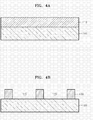
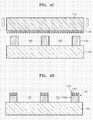
- FIGS. 4A through 4D are cross-sectional views illustrating a method of manufacturing the black matrix 120.
- a light shade layer 110 formed of an ink-philic material is formed on the substrate 100.
- the light shade layer 110 may be formed by coating the ink-philic material to a predetermined thickness on the substrate 100 and soft baking the same.
- the substrate 100 is transparent and may be a glass substrate or a plastic substrate.
- the ink-philic material may be polymer-based organic resin.
- the ink-philic material may be coated on the substrate 100 using a method, such as, spin coating, die coating, or dip coating.
- the soft baking may be executed at about 80-120 °C for about 30 seconds to 2 minutes.
- the light shade layer 110 is patterned into a patterned light shade layer 120'.
- the patterned light shade layer 120' defines a plurality of pixel regions 140 on the substrate 100.
- the patterning of the light shade layer 110 may be achieved by exposing the light shade layer 110 to light using a photomask (not shown) having a predetermined pattern.
- photoresist (not shown) is coated on the surface of the light shade layer 110 and patterned by lithography.
- the light shade layer 110 is etched using the patterned photoresist as an etch mask.
- the patterned light shade layer 120' may be about 1.5 ⁇ m in height and about 30 ⁇ m in width.
- the patterned light shade layer 120' is hard baked.
- the hard baking may be performed at about 200-230 ° C for about 20 - 40 minutes.
- the nano-sized grooves may be formed on the upper surface of the patterned light shade layer 120' using a nano-imprinting process.
- a stamp 150 is installed over the patterned light shade layer 120'.
- the stamp 150 has nano-sized protrusions 160 formed on its bottom.
- the stamp 150 may be formed of a material selected from the group consisting of glass, quartz, silicon (Si), and poly(dimethylsiloxane) (PDMS).
- PDMS poly(dimethylsiloxane)
- the grooves 130 formed on the upper surface 120a of the black matrix 120 using the nano-imprinting process may be about 20-200nm in size and about 1000-100000nm 2 , preferably, about 5000-10000nm 2 , in cross-sectional area.
- the grooves 130 may occupy 20-50% of the upper surface 120a of the black matrix 120.
- the depth of each of the grooves 130 may be about 50-200nm.
- the nano-sized grooves 130 are formed on the upper surface 120a of the black matrix 120, the upper surface 120a is rendered ink-phobic, and the lateral surfaces 120b of the black matrix 120 are rendered ink-philic.
- the upper surface of a black matrix according to the present invention may be rendered ink-phobic by making the upper surface of the black matrix have a concavo-convex structure using a physical method.
- a color filter is manufactured using the black matrix, ink mixture between pixels of the color filter can be prevented.
- the lateral surfaces of the black matrix are kept ink-philic, the color reproducibility and contrast ratio of the color filter can be improved.
Landscapes
- Physics & Mathematics (AREA)
- General Physics & Mathematics (AREA)
- Optics & Photonics (AREA)
- Engineering & Computer Science (AREA)
- Manufacturing & Machinery (AREA)
- Optical Filters (AREA)
- Liquid Crystal (AREA)
- Optical Elements Other Than Lenses (AREA)
Abstract
Description
- The present invention relates to a black matrix of a color filter, and more particularly, a black matrix for color filters by which ink mixture between pixels of a color filter may be prevented and the color reproducibility and contrast ratio of the color filter may be improved, and a method of manufacturing the black matrix.
- Up to now, cathode ray tube (CRT) monitors have been usually used to display information from TVs and computers. However, recently, flat panel displays, such as, liquid crystal displays (LCDs), plasma display panels (PDPs), electro-luminescence (EL) displays, light emitting diodes (LEDs), or field emission displays (FEDs), are being used with a recent increase in the sizes of screens. LCDs among these flat panel displays are widely used as desk-top computer monitors, lap-top computer monitors, etc. because of low power consumption.
- General LCDs include a color filter that forms images of desired colors by transmitting white light modulated by a liquid crystal layer. To manufacture a color filter, first, a black matrix having a predetermined shape is formed on a transparent substrate, and then inks of predetermined colors, such as, red (R), green (G), and blue (B), are injected into pixel regions defined by the black matrix using an inkjet printing method, for example, to form pixels of the predetermined colors.
- In the manufacture of the color filter, when an upper surface and a lateral surface of the black matrix are both ink-philic, ink injected into each pixel region may overflow onto the upper surface ink and thus color mixture between pixels may occur. On the other hand, when the upper surface and the lateral surface of the black matrix are both ink-phobic, the ink mixture between pixels can be prevented, but ink coated within each pixel region cannot have a uniform thickness due to the lack of wetting of the lateral surface of the black matrix with ink. Hence, light leakage around the lateral surfaces of the black matrix may occur, consequently degrading the color reproducibility and the contrast ratio of the color filter.
- Therefore, to address the ink mixture and light leakage problems, it is desirable to render the upper surface of the black matrix ink-phobic and the lateral surface thereof ink-philic.
- The present invention provides a black matrix for color filters by which ink mixture between pixels of a color filter may be prevented and the color reproducibility and contrast ratio of the color filter may be improved, and a method of manufacturing the black matrix.
- According to an aspect of the present invention, there is provided a black matrix for color filters that is formed on a substrate and defines a plurality of pixel regions, the black matrix including: an upper surface having a plurality of nano-sized grooves formed therein and being ink-phobic; and lateral surfaces being ink-philic.
- The black matrix may be formed of an ink-philic material. The black matrix may be formed of polymer-based organic resin.
- Each of the grooves may be 20-200nm in size and 1000-100000nm2 in cross-sectional area. The grooves may occupy 20-50% of the upper surface. Each of the grooves may be 50-200nm in depth.
- According to another aspect of the present invention, there is provided a color filter including: a substrate; a black matrix formed on a substrate and defining a plurality of pixel regions; and ink of predetermined colors filled within the pixel regions. The black matrix include: an upper surface having a plurality of nano-sized grooves formed therein and being ink-phobic; and lateral surfaces being ink-philic.
- According to another aspect of the present invention, there is provided a method of manufacturing a black matrix for color filters, the method comprising the operations of: forming a light shade layer of an ink-philic material on a substrate; patterning the light shade layer to define a plurality of pixel regions on the substrate; and forming a black matrix by forming nano-sized grooves on an upper surface of the patterned light shade layer using a nano-imprinting process.
- The operation of forming the light shade layer may include: coating the ink-philic material on the substrate; and soft baking the ink-philic material. After the patterning of the light shade layer, the operation of hard baking the patterned light shade layer may be further included. In this case, the nano-imprinting process may be executed during the hard baking of the patterned light shade layer.
- The operation of forming the grooves using the nano-imprinting process may include: installing a stamp over the patterned light shade layer, the stamp having nano-sized protrusions formed on its bottom; pressing the stamp down on the upper surface of the patterned light shade layer so as to form grooves having shapes depending on the shapes of the protrusions in the upper surface of the patterned light shade layer; and separating the stamp from the light shade layer.
- The stamp may be formed of a material selected from the group consisting of glass, quartz, silicon (Si), and poly(dimethylsiloxane) (PDMS).
- According to yet another aspect of the invention, there is provided a black matrix for color filters that is formed on a substrate and defines a plurality of pixel regions on the substrate for receiving a predetermined ink, the black matrix comprising: an upper surface being formed such that it repels the predetermined ink; and lateral surfaces that are formed such that they do not repel the predetermined ink.
- The above and other features and advantages of the present invention will become more apparent by describing in detail exemplary embodiments thereof with reference to the attached drawings in which:
- FIG. 1 is a perspective view of a black matrix of a color filter according to an embodiment of the present invention;
- FIG. 2 is a cross-section of the black matrix shown in FIG. 1;
- FIG. 3 is a color filter manufactured using the black matrix shown in FIGS. 1 and 2; and
- FIGS. 4A through 4D are cross-sectional views illustrating a method of manufacturing the black matrix shown in FIGS. 1 and 2.
- The present invention will now be described more fully with reference to the accompanying drawings, in which exemplary embodiments of the invention are shown. In the drawings, the thicknesses of elements are exaggerated for clarity. Like reference numerals in the drawings denote like elements, and thus their description will be omitted.
- FIG. 1 is a perspective view of a
black matrix 120 of a color filter according to an embodiment of the present invention. FIG. 2 is a cross-section of the black matrix shown in FIG. 1. - Referring to FIGS. 1 and 2, the
black matrix 120 having a predetermined shape is formed on asubstrate 100. A plurality ofpixel regions 140 are defined on thesubstrate 100 by theblack matrix 120. Each of thepixel regions 140 is filled with ink of a predetermined color, and thus pixels are formed. Consequently, a color filter made up of the pixels is formed. - The
substrate 100 is transparent, and a glass substrate or a plastic substrate may be used as thetransparent substrate 100. Theblack matrix 120 is formed of an ink-philic material. Theblack matrix 120 may be formed of polymer-based organic resin. Theblack matrix 120 may have a height of about 1.5µ m and a width of about 30µ m. - An
upper surface 120a of theblack matrix 120 may have a concavo-convex structure. More specifically, nano-sized grooves 130 are formed on theupper surface 120a of theblack matrix 120. Although thegrooves 130 having circular horizontal cross-sections are illustrated in FIG. 1, the cross-sections of thegrooves 130 are not limited to circles but may have the other various cross-section shapes. In the present embodiment, thegrooves 130 may occupy 10-60% of theupper surface 120a of theblack matrix 120. Each of thegrooves 130 may be about, 10-500nm, preferably about 20-200nm, in size and about 1000-100000nm2, preferably, about 5000-10000nm2, in cross-sectional area. The size of each of thegrooves 130 denotes the diameter of eachgroove 130 or a maximum distance between inner walls of eachgroove 130. The depth of each of thegrooves 130 may be about 20-500nm, preferably 50-200nm. - As described above, when the nano-sized
grooves 130 are formed on theupper surface 120a of theblack matrix 120, theupper surface 120a is rendered ink-phobic. The reason why theupper surface 120a of theblack matrix 120 formed of an ink-philic material has an ink-phobic characteristics is due to a lotus effect. More specifically, when the nano-sizedgrooves 130 are formed on theupper surface 120a of theblack matrix 120, theupper surface 120a is made up of a surface of the material of theblack matrix 120 and the air filled within thegrooves 130. Accordingly, when the nano-sizedgrooves 130 are formed on theupper surface 120a of theblack matrix 120, an area of theupper surface 120a that contacts ink is reduced compared with when theupper surface 120a of theblack matrix 120 has no concave-convex structures, that is, is flat. Hence, the surface energy on theupper surface 120a in which thegrooves 130 are formed is reduced, and the contact angle with respect to ink is increased. Consequently, theupper surface 120a having thegrooves 130 is rendered ink-phobic. For example, given that the contact angle of a flat plane formed of a certain material with respect to ink is approximately 10, when nano-sized grooves are formed on the flat plane so that air occupies 30% of the flat plane, the contact angle of the plane having the grooves with respect to ink is increased to about 67° . - As described above, the
upper surface 120a of theblack matrix 120 is processed to have a concavo-convex structure using a physical method instead of changing the component of theblack matrix 120 or chemically processing the surface of theblack matrix 120, so that theupper surface 120a of theblack matrix 120 is rendered ink-phobic. -
Lateral surfaces 120b of theblack matrix 120 formed of an ink-philic material are kept ink-philic. - In other words, the
upper surface 120a having thegrooves 130 has a tendency to repel, not combine with, or not attract ink. Conversely,lateral surfaces 120b are formed such that they have a tendency to attract, combine with, or not repel ink. - The ink may be a water-based ink and may be suitable for being injected or inkjet printed.
- FIG. 3 is a color filter manufactured using the
black matrix 120. Referring to FIG. 3, the color filter includes thesubstrate 100, theblack matrix 120 formed on the substrate 10 and defining pixel regions, and ink of predetermined colors, such as, red (R), green (G), and blue (B), filled in the regions. - As described above, since the
upper surface 120a of theblack matrix 120 has the nano-sized grooves 130 formed therein, theupper surface 120a is ink-phobic. Accordingly, when pixels are formed by injecting ink into the pixel regions using an inkjet printing method, for example, color mixture between pixels can be prevented. In addition, since the lateral surfaces 120b of theblack matrix 120 are ink-philic, ink can be coated within the pixel regions to have uniform thicknesses. Hence, the color reproducibility and the contrast ratio of the color filter can be improved. - FIGS. 4A through 4D are cross-sectional views illustrating a method of manufacturing the
black matrix 120. Referring to FIG. 4A, alight shade layer 110 formed of an ink-philic material is formed on thesubstrate 100. Thelight shade layer 110 may be formed by coating the ink-philic material to a predetermined thickness on thesubstrate 100 and soft baking the same. Thesubstrate 100 is transparent and may be a glass substrate or a plastic substrate. The ink-philic material may be polymer-based organic resin. The ink-philic material may be coated on thesubstrate 100 using a method, such as, spin coating, die coating, or dip coating. The soft baking may be executed at about 80-120 °C for about 30 seconds to 2 minutes. - Referring to FIG. 4B, the
light shade layer 110 is patterned into a patterned light shade layer 120'. The patterned light shade layer 120' defines a plurality ofpixel regions 140 on thesubstrate 100. When thelight shade layer 110 is formed of a photosensitive material, the patterning of thelight shade layer 110 may be achieved by exposing thelight shade layer 110 to light using a photomask (not shown) having a predetermined pattern. On the other hand, when thelight shade layer 110 is formed of a non-photosensitive material, photoresist (not shown) is coated on the surface of thelight shade layer 110 and patterned by lithography. Thelight shade layer 110 is etched using the patterned photoresist as an etch mask. The patterned light shade layer 120' may be about 1.5 µ m in height and about 30 µ m in width. - Thereafter, the patterned light shade layer 120' is hard baked. The hard baking may be performed at about 200-230 ° C for about 20 - 40 minutes. While the patterned light shade layer 120' is being hard baked, the nano-sized grooves (see FIG. 4D) may be formed on the upper surface of the patterned light shade layer 120' using a nano-imprinting process.
- More specifically, referring to FIG. 4C, first, a
stamp 150 is installed over the patterned light shade layer 120'. Thestamp 150 has nano-sized protrusions 160 formed on its bottom. Thestamp 150 may be formed of a material selected from the group consisting of glass, quartz, silicon (Si), and poly(dimethylsiloxane) (PDMS). Next, when thestamp 150 is pressed down on the upper surface of the patterned light shade layer 120' , theprotrusions 160 formed on the bottom surface of thestamp 150 enter into the upper surface of the patterned light shade layer 120' , so that the grooves 130 (see FIG. 4D) having shapes depending on the shapes of theprotrusions 160 are formed in the upper surface of the patterned light shade layer 120' . At this time, since the patterned light shade layer 120' is rendered soft during the hard baking, theprotrusions 160 of thestamp 150 can easily squeeze into the upper surface of the patterned light shade layer 120'. - Then, when the
stamp 150 is taken away, theblack matrix 120 is completely formed. Thegrooves 130 formed on theupper surface 120a of theblack matrix 120 using the nano-imprinting process may be about 20-200nm in size and about 1000-100000nm2, preferably, about 5000-10000nm2, in cross-sectional area. Thegrooves 130 may occupy 20-50% of theupper surface 120a of theblack matrix 120. The depth of each of thegrooves 130 may be about 50-200nm. As described above, when the nano-sized grooves 130 are formed on theupper surface 120a of theblack matrix 120, theupper surface 120a is rendered ink-phobic, and the lateral surfaces 120b of theblack matrix 120 are rendered ink-philic. - Although a black matrix for a color filter usually used in LCDs and a method of fabricating the black matrix have been illustrated, the structure of the black matrix and the fabrication thereof may be equally applied to banks that are used in organic ELs (OLEDs).
- As described above, the upper surface of a black matrix according to the present invention may be rendered ink-phobic by making the upper surface of the black matrix have a concavo-convex structure using a physical method. Thus, when a color filter is manufactured using the black matrix, ink mixture between pixels of the color filter can be prevented. Furthermore, since the lateral surfaces of the black matrix are kept ink-philic, the color reproducibility and contrast ratio of the color filter can be improved.
- While the present invention has been particularly shown and described with reference to exemplary embodiments thereof, it will be understood by those of ordinary skill in the art that various changes in form and details may be made therein without departing from the scope of the present invention as defined by the following claims.
Claims (23)
- A black matrix (120) for color filters that is formed on a substrate (100) and defines a plurality of pixel regions (140) on the substrate for receiving a predetermined ink, the black matrix (120) comprising:an upper surface (120a) having a plurality of nano-sized grooves (130) formed therein and being ink-phobic; andlateral surfaces arranged to define the plurality of pixel regions (140) and to be ink-philic.
- The black matrix for color filters of claim 1, wherein the upper surface (120a) is ink-phobic due to a locus effect which is caused by the nano-sized grooves (130).
- The black matrix for color filters of claim 1 or 2, wherein the black matrix (120) is formed of an ink-philic material.
- The black matrix for color filters of claim 3, wherein the black matrix (120) is formed of polymer-based organic resin.
- The black matrix for color filters of claim 1, 2, 3 or 4, wherein each of the grooves (130) is 20-200nm in size.
- The black matrix for color filters of any preceding claim, wherein each of the grooves (130) is 1000-100000nm2 in cross-sectional area.
- The black matrix for color filters of any preceding claim, wherein the grooves (130) occupy 20-50% of the upper surface.
- The black matrix for color filters of any preceding claim, wherein each of the grooves is 50-200nm in depth.
- The black matrix for color filters of any preceding claim, wherein the ink is suitable for inject printing.
- A color filter comprising:a black matrix according to any preceding claim; andink of predetermined colors filled within the pixel regions (140).
- A method of manufacturing a black matrix for color filters, the method comprising:forming a light shade layer (110) of an ink-philic material on a substrate (100);patterning the light shade layer (110) to define a plurality of pixel regions (140) on the substrate (100); andforming a black matrix (120) by forming nano-sized grooves (130) on an upper surface of the patterned light shade layer (120) using a nano-imprinting process.
- The method of claim 11, wherein the light shade layer (110) is formed of polymer-based organic resin.
- The method of claim 11, wherein the forming of the light shade layer (110) comprises:coating the ink-philic material on the substrate (100); andsoft baking the ink-philic material.
- The method of claim 13, wherein the soft baking is performed at 80-120°C.
- The method of any of claims 11 to 14, after the patterning of the light shade layer (110), further comprising hard baking the patterned light shade layer (120).
- The method of claim 15, wherein the hard baking is performed at approximately 200-230°C.
- The method of claim 15 or 16, wherein the nano-imprinting process is executed during the hard baking of the patterned light shade layer (120).
- The method of any of claims 11 to 17, wherein the forming of the grooves (130) using the nano-imprinting process comprises:installing a stamp (150) over the patterned light shade layer (120), the stamp (130) having nano-sized protrusions (160) formed on its bottom;pressing the stamp down (150) on the upper surface of the patterned light shade layer (120) so as to form grooves (130) having shapes depending on the shapes of the protrusions (160) in the upper surface of the patterned light shade layer (120); andseparating the stamp (150) from the light shade layer (120).
- The method of claim 18, wherein the stamp (150) is formed of a material selected from the group consisting of glass, quartz, silicon, and polydimethylsiloxane.
- The method of any of claims 11 to 19, wherein each of the grooves (130) is formed to have a size of 20-200nm.
- The method of any of claims 11 to 20, wherein each of the grooves (130) is formed to have a cross-sectional area of 1000-100000nm2.
- The method of any of claims 11 to 21, wherein the grooves (130) occupy 20-50% of the upper surface of the black matrix.
- The method of any of claims 11 to 22, wherein each of the grooves (130) is formed to have a depth of 50-200nm.
Applications Claiming Priority (1)
| Application Number | Priority Date | Filing Date | Title |
|---|---|---|---|
| KR1020060001675A KR100790866B1 (en) | 2006-01-06 | 2006-01-06 | Black matrix for color filters and manufacturing method thereof |
Publications (2)
| Publication Number | Publication Date |
|---|---|
| EP1806602A2 true EP1806602A2 (en) | 2007-07-11 |
| EP1806602A3 EP1806602A3 (en) | 2007-11-07 |
Family
ID=38001962
Family Applications (1)
| Application Number | Title | Priority Date | Filing Date |
|---|---|---|---|
| EP06122875A Withdrawn EP1806602A3 (en) | 2006-01-06 | 2006-10-24 | Black matrix of color filter and method of manufacturing the black matrix |
Country Status (4)
| Country | Link |
|---|---|
| US (1) | US20070157839A1 (en) |
| EP (1) | EP1806602A3 (en) |
| JP (1) | JP2007183587A (en) |
| KR (1) | KR100790866B1 (en) |
Cited By (2)
| Publication number | Priority date | Publication date | Assignee | Title |
|---|---|---|---|---|
| EP2186118A4 (en) * | 2007-08-28 | 2013-10-23 | Agency Science Tech & Res | METHOD FOR MANUFACTURING ORGANIC ELECTRONIC OR OPTOELECTRONIC DEVICE |
| WO2015189735A1 (en) * | 2014-06-13 | 2015-12-17 | Semiconductor Energy Laboratory Co., Ltd. | Display device |
Families Citing this family (19)
| Publication number | Priority date | Publication date | Assignee | Title |
|---|---|---|---|---|
| KR100785031B1 (en) * | 2006-11-22 | 2007-12-12 | 삼성전자주식회사 | Black matrix for color filters and manufacturing method thereof |
| WO2009113615A1 (en) * | 2008-03-13 | 2009-09-17 | 富士フイルム株式会社 | Photosensitive resin composition, photosensitive resin hardened film, and method for forming light-shielding image |
| KR20100123973A (en) * | 2009-05-18 | 2010-11-26 | 삼성전자주식회사 | Color filter, apparatus for manufacturing the same and method for manufacturing the same |
| JP2010286615A (en) * | 2009-06-10 | 2010-12-24 | Sony Corp | OPTICAL COMPONENT MANUFACTURING METHOD, OPTICAL COMPONENT, DISPLAY DEVICE MANUFACTURING METHOD, AND DISPLAY DEVICE |
| KR101591922B1 (en) | 2009-10-20 | 2016-02-05 | 삼성디스플레이 주식회사 | Display board |
| KR20140119266A (en) * | 2013-03-28 | 2014-10-10 | 삼성디스플레이 주식회사 | Organic light emitting display device and manufacturing method thereof |
| WO2015072316A1 (en) * | 2013-11-14 | 2015-05-21 | 堺ディスプレイプロダクト株式会社 | Color filter substrate, display device, and method for manufacturing color filter substrate |
| CN104882468B (en) * | 2015-06-09 | 2017-12-15 | 京东方科技集团股份有限公司 | Organic electroluminescent display substrate and preparation method thereof, display device |
| US11207478B2 (en) | 2016-03-25 | 2021-12-28 | Rai Strategic Holdings, Inc. | Aerosol production assembly including surface with micro-pattern |
| US9955584B2 (en) * | 2016-04-25 | 2018-04-24 | Winbond Electronics Corp. | Stamp for printed circuit process and method of fabricating the same and printed circuit process |
| US11297876B2 (en) * | 2017-05-17 | 2022-04-12 | Rai Strategic Holdings, Inc. | Aerosol delivery device |
| KR102179729B1 (en) | 2018-03-27 | 2020-11-17 | 주식회사 엘지화학 | Black partition wall pattern film and method for manufacturing thereof |
| CN110534548A (en) * | 2019-08-06 | 2019-12-03 | 武汉华星光电半导体显示技术有限公司 | OLED display panel |
| CN110993646B (en) * | 2019-11-08 | 2022-07-12 | 深圳市华星光电半导体显示技术有限公司 | Preparation method of OLED (organic light emitting diode) back plate and OLED back plate |
| KR102934063B1 (en) | 2020-06-05 | 2026-03-04 | 삼성디스플레이 주식회사 | Display apparatus |
| KR102892879B1 (en) | 2020-06-22 | 2025-11-28 | 삼성디스플레이 주식회사 | Display apparatus |
| CN111769143B (en) * | 2020-06-23 | 2022-09-09 | 武汉华星光电半导体显示技术有限公司 | Display panel and manufacturing method thereof |
| KR20220110409A (en) | 2021-01-29 | 2022-08-08 | 삼성디스플레이 주식회사 | Display device |
| CN113013211B (en) | 2021-02-24 | 2022-10-25 | 京东方科技集团股份有限公司 | Display substrate, preparation method thereof and display device |
Family Cites Families (24)
| Publication number | Priority date | Publication date | Assignee | Title |
|---|---|---|---|---|
| JPS5975205A (en) * | 1982-10-25 | 1984-04-27 | Seiko Epson Corp | Color filter manufacturing method |
| JPH07104117A (en) * | 1993-09-30 | 1995-04-21 | Sekisui Chem Co Ltd | Color filter for display |
| JP2872594B2 (en) * | 1993-11-24 | 1999-03-17 | キヤノン株式会社 | Method for manufacturing color filter and method for manufacturing liquid crystal panel |
| JP2000162425A (en) * | 1998-11-30 | 2000-06-16 | Canon Inc | Color filter, manufacturing method thereof, and liquid crystal element |
| GB9929752D0 (en) * | 1999-12-17 | 2000-02-09 | Secr Defence | Textured surface |
| JP2001183516A (en) * | 1999-12-27 | 2001-07-06 | Canon Inc | Color filter, method of manufacturing the same, and liquid crystal element using the color filter |
| JP2002006129A (en) * | 2000-06-19 | 2002-01-09 | Canon Inc | Optical element, manufacturing method thereof, and liquid crystal element |
| KR100835912B1 (en) | 2001-10-19 | 2008-06-09 | 엘지디스플레이 주식회사 | Method for manufacturing color filter substrate of liquid crystal display |
| KR100469390B1 (en) | 2001-12-27 | 2005-02-02 | 엘지전자 주식회사 | Color filter manufacturing method for lcd |
| EP1474835A1 (en) * | 2002-02-01 | 2004-11-10 | Koninklijke Philips Electronics N.V. | Structured polmer substrate for ink-jet printing of an oled matrix |
| JP2004111166A (en) * | 2002-09-18 | 2004-04-08 | Hitachi Ltd | Substrate with bank for organic EL device |
| GB0302485D0 (en) * | 2003-02-04 | 2003-03-05 | Plastic Logic Ltd | Pixel capacitors |
| JP2005063785A (en) * | 2003-08-11 | 2005-03-10 | Ran Technical Service Kk | Partition pattern and method for forming the same |
| US7156032B2 (en) * | 2003-08-22 | 2007-01-02 | Lucent Technologies Inc. | Method and apparatus for controlling friction between a fluid and a body |
| JP4317113B2 (en) * | 2003-10-30 | 2009-08-19 | 三星モバイルディスプレイ株式會社 | Manufacturing method of flat panel display device |
| JP2005173107A (en) * | 2003-12-10 | 2005-06-30 | Dainippon Printing Co Ltd | Optical sheet with light shielding layer and color filter |
| JP5005164B2 (en) * | 2004-03-03 | 2012-08-22 | 株式会社ジャパンディスプレイイースト | LIGHT EMITTING ELEMENT, LIGHT EMITTING DISPLAY DEVICE AND LIGHTING DEVICE |
| US20050211505A1 (en) * | 2004-03-26 | 2005-09-29 | Kroupenkine Timofei N | Nanostructured liquid bearing |
| US7172842B2 (en) * | 2004-05-12 | 2007-02-06 | Chunghwa Picture Tubes, Ltd. | Color filter array plate and method of fabricating the same |
| JP2006072176A (en) * | 2004-09-06 | 2006-03-16 | Seiko Epson Corp | Bank, color filter, display device and electronic device |
| KR20060024949A (en) | 2004-09-15 | 2006-03-20 | 삼성전자주식회사 | Color filter substrate and its manufacturing method |
| DE202004018784U1 (en) * | 2004-12-03 | 2005-03-17 | Koob Ron | Motor vehicle reversing camera housing has nanotechnoligical coating to reduce soiling |
| KR20060080760A (en) | 2005-01-06 | 2006-07-11 | 삼성전자주식회사 | Color filter substrate and its manufacturing method |
| JP4327108B2 (en) * | 2005-02-03 | 2009-09-09 | 株式会社リコー | Optical information recording medium manufacturing method and mold manufacturing method |
-
2006
- 2006-01-06 KR KR1020060001675A patent/KR100790866B1/en not_active Expired - Lifetime
- 2006-10-20 US US11/583,831 patent/US20070157839A1/en not_active Abandoned
- 2006-10-24 EP EP06122875A patent/EP1806602A3/en not_active Withdrawn
- 2006-12-01 JP JP2006326097A patent/JP2007183587A/en active Pending
Cited By (4)
| Publication number | Priority date | Publication date | Assignee | Title |
|---|---|---|---|---|
| EP2186118A4 (en) * | 2007-08-28 | 2013-10-23 | Agency Science Tech & Res | METHOD FOR MANUFACTURING ORGANIC ELECTRONIC OR OPTOELECTRONIC DEVICE |
| WO2015189735A1 (en) * | 2014-06-13 | 2015-12-17 | Semiconductor Energy Laboratory Co., Ltd. | Display device |
| US20150362776A1 (en) | 2014-06-13 | 2015-12-17 | Semiconductor Energy Laboratory Co., Ltd. | Display Device |
| US10342124B2 (en) | 2014-06-13 | 2019-07-02 | Semiconductor Energy Laboratory Co., Ltd. | Display device |
Also Published As
| Publication number | Publication date |
|---|---|
| KR20070074051A (en) | 2007-07-12 |
| EP1806602A3 (en) | 2007-11-07 |
| JP2007183587A (en) | 2007-07-19 |
| US20070157839A1 (en) | 2007-07-12 |
| KR100790866B1 (en) | 2008-01-03 |
Similar Documents
| Publication | Publication Date | Title |
|---|---|---|
| US20070157839A1 (en) | Black matrix of color filter and method of manufacturing the black matrix | |
| CN107393939B (en) | Pixel defining layer and manufacturing method thereof, display panel and manufacturing method thereof, and display device | |
| CN108538886B (en) | Pixel definition layer and manufacturing method, display substrate, and display device | |
| CN107248523B (en) | Pixel defining layer and manufacturing method thereof | |
| WO2016086728A1 (en) | Pixel definition layer and manufacturing method therefor, display panel and display device | |
| CN104979484A (en) | Organic light emitting diode display device and method of fabricating the same | |
| CN108630734B (en) | Pixel-defining structure and preparation method thereof, and display panel and display device | |
| CN107623022A (en) | Pixel defining layer and manufacturing method thereof, display substrate and manufacturing method thereof, display device | |
| EP4170721A1 (en) | Display panel and manufacturing method therefor | |
| JP5037145B2 (en) | Color filter manufacturing method | |
| US7816010B2 (en) | Black matrix for color filter and its method of manufacture | |
| CN101013220B (en) | Method of fabricating black matrices of color filter | |
| US20070184363A1 (en) | Method of manufacturing a black matrix of color filter | |
| US20080124634A1 (en) | Method of manufacturing liquid crystal display | |
| CN102183806A (en) | Color filter array and manufacturing method thereof | |
| CN101013219B (en) | Method for preparing black matrix of color filter | |
| US20080166641A1 (en) | Method of manufacturing color filter | |
| CN210428036U (en) | Color electronic ink display screen structure | |
| US20090017388A1 (en) | Substrate structure for color filter and color filter having the same | |
| EP1818695A1 (en) | Apparatus for fabricating color filter | |
| CN112271200A (en) | Display panel, method for producing the same, and display device | |
| EP1607996A2 (en) | Method of manufacturing phosphor layer structure | |
| US20090011344A1 (en) | Method of manufacturing color filter |
Legal Events
| Date | Code | Title | Description |
|---|---|---|---|
| PUAI | Public reference made under article 153(3) epc to a published international application that has entered the european phase |
Free format text: ORIGINAL CODE: 0009012 |
|
| AK | Designated contracting states |
Kind code of ref document: A2 Designated state(s): AT BE BG CH CY CZ DE DK EE ES FI FR GB GR HU IE IS IT LI LT LU LV MC NL PL PT RO SE SI SK TR |
|
| AX | Request for extension of the european patent |
Extension state: AL BA HR MK YU |
|
| PUAL | Search report despatched |
Free format text: ORIGINAL CODE: 0009013 |
|
| AK | Designated contracting states |
Kind code of ref document: A3 Designated state(s): AT BE BG CH CY CZ DE DK EE ES FI FR GB GR HU IE IS IT LI LT LU LV MC NL PL PT RO SE SI SK TR |
|
| AX | Request for extension of the european patent |
Extension state: AL BA HR MK YU |
|
| 17P | Request for examination filed |
Effective date: 20080206 |
|
| 17Q | First examination report despatched |
Effective date: 20080305 |
|
| AKX | Designation fees paid |
Designated state(s): DE FR GB |
|
| GRAP | Despatch of communication of intention to grant a patent |
Free format text: ORIGINAL CODE: EPIDOSNIGR1 |
|
| STAA | Information on the status of an ep patent application or granted ep patent |
Free format text: STATUS: THE APPLICATION IS DEEMED TO BE WITHDRAWN |
|
| 18D | Application deemed to be withdrawn |
Effective date: 20111006 |