EP1804294A1 - Method for manufacturing non volatile memory cells - Google Patents
Method for manufacturing non volatile memory cells Download PDFInfo
- Publication number
- EP1804294A1 EP1804294A1 EP05425943A EP05425943A EP1804294A1 EP 1804294 A1 EP1804294 A1 EP 1804294A1 EP 05425943 A EP05425943 A EP 05425943A EP 05425943 A EP05425943 A EP 05425943A EP 1804294 A1 EP1804294 A1 EP 1804294A1
- Authority
- EP
- European Patent Office
- Prior art keywords
- layer
- openings
- semiconductor substrate
- surface portions
- insulation layer
- Prior art date
- Legal status (The legal status is an assumption and is not a legal conclusion. Google has not performed a legal analysis and makes no representation as to the accuracy of the status listed.)
- Withdrawn
Links
Images


Classifications
-
- H—ELECTRICITY
- H10—SEMICONDUCTOR DEVICES; ELECTRIC SOLID-STATE DEVICES NOT OTHERWISE PROVIDED FOR
- H10B—ELECTRONIC MEMORY DEVICES
- H10B41/00—Electrically erasable-and-programmable ROM [EEPROM] devices comprising floating gates
- H10B41/30—Electrically erasable-and-programmable ROM [EEPROM] devices comprising floating gates characterised by the memory core region
-
- H—ELECTRICITY
- H10—SEMICONDUCTOR DEVICES; ELECTRIC SOLID-STATE DEVICES NOT OTHERWISE PROVIDED FOR
- H10B—ELECTRONIC MEMORY DEVICES
- H10B69/00—Erasable-and-programmable ROM [EPROM] devices not provided for in groups H10B41/00 - H10B63/00, e.g. ultraviolet erasable-and-programmable ROM [UVEPROM] devices
-
- H—ELECTRICITY
- H10—SEMICONDUCTOR DEVICES; ELECTRIC SOLID-STATE DEVICES NOT OTHERWISE PROVIDED FOR
- H10D—INORGANIC ELECTRIC SEMICONDUCTOR DEVICES
- H10D64/00—Electrodes of devices having potential barriers
- H10D64/01—Manufacture or treatment
- H10D64/031—Manufacture or treatment of data-storage electrodes
- H10D64/035—Manufacture or treatment of data-storage electrodes comprising conductor-insulator-conductor-insulator-semiconductor structures
Definitions
- the present invention relates to a method for manufacturing non volatile memory cells integrated on a semiconductor substrate.
- the invention relates to a method for manufacturing non volatile memory cells integrated on a semiconductor substrate, each one comprising a floating gate electrode, the method comprising the steps of:
- the invention relates, in particular but not exclusively, to a method for manufacturing non-volatile memory cells integrated in Flash memory electronic devices and the following description is made with reference to this field of application by way of illustration only.
- non volatile memory electronic devices of the Flash type integrated on semiconductor comprise a plurality of non-volatile memory cells organised in matrix; i.e. the cells are organised in rows, called word lines, and columns, called bit lines.
- Each single non volatile memory cell comprises a MOS transistor integrated on a semiconductor substrate wherein the so called gate electrode, arranged above the channel region, is floating, i.e. it has a high DC impedance towards all the other terminals of the same cell and of the circuit wherein the cell is inserted.
- the gate electrode is insulated from the semiconductor substrate, and thus from the channel region, at least by means of a dielectric layer called tunnel oxide.
- the cell also comprises a second so called control gate electrode, which is driven by means of suitable control voltages.
- the other electrodes of the transistors are the usual drain, source terminals.
- Flash memories Some known process steps to form these Flash memories, i.e. provided with a floating gate electrode, organised in matrix are shown in figures 1-5. In these figures some vertical section views are shown of the memory cells in a direction parallel to the "Word Lines", but in a different plane respect to this latter so as to highlight the evolution of the standard process flow in these areas.
- insulation structures of the STI type are formed on the semiconductor substrate 1 .
- a sacrificial oxide layer 2 and a nitride layer 3 are formed in sequence.
- nitride layer 3 On the nitride layer 3 a photolithographic mask provided with openings is then formed.
- the nitride layer 3 is etched so as to form first openings 4.
- the walls of these openings 4 are vertical or tapered downwards, i.e. the width of the vertical section of the opening 4 is not constant and it decreases approaching the semiconductor substrate 1.
- the sacrificial oxide layer 2 is then etched so as to form second openings 5.
- the walls of these openings 5 are vertical or tapered downwards.
- an oxide layer 7 called field oxide is then formed so as to fill in the trenches 6, the first and the second openings 4, 5.
- the nitride layer 3 and the sacrificial oxide layer 2 are completely removed.
- Superficial portions 7a of the field oxide layer 7 then project from the semiconductor substrate 1 and are divided from each other by third openings 7b which have side walls being vertical with respect to the surface of the semiconductor substrate 1 or these side walls diverge approaching the semiconductor substrate 1.
- the third openings 7b have in fact the same shape as the one of the nitride layer 3 and of the sacrificial oxide layer 2 after the formation of the first and second openings 4, 5.
- the side walls of the surface portions 7a of the field oxide layer 7 are vertical or tapered downwards i.e. their cross dimensions decrease approaching the semiconductor substrate 1.
- the walls of the surface portions 7a of the field oxide layer 7 follow the profile of the first and second openings 4 and 5, while the portions of the field oxide layer 7 formed inside the semiconductor substrate 1 follow the profile of the trench 6.
- a so called tunnel oxide layer 8 is then formed on the exposed surface of the semiconductor substrate 1.
- a polysilicon layer 9 or amorphous silicon is then deposited on the whole device.
- polysilicon and amorphous silicon are conformal materials, i.e. they tend to follow the profile of the surface whereon they are deposited, therefore during the deposition step of the polysilicon layer 9, if the aspect ratio (ratio between the height and the width) of the third openings 7b is higher than 0.5:1, the deposition fronts formed on the side walls of the surface portions 7a of the field oxide layer 7, i.e. inside the third openings 7b, touch each other before the deposition front formed on the tunnel layer 8 can completely fill in the space comprised between adjacent surface portions 7a of the field oxide layer 7, thus forming voids 10 inside the polysilicon layer 9.
- voids 10 are formed inside the polysilicon layer any time the cross dimensions of the third openings 7b are smaller than the double of their depth.
- the deposition of the polysilicon layer 9 is continued until the surface portions 7a of the field oxide layer 7 are completely covered.
- a removal step of the polysilicon layer 9 is made follow at least until the surface portions 7a of the field oxide layer 7 are expose. Portions of the polysilicon layer 9 remaining confined between the surface portions 7a of the field oxide layer 7 form floating gate electrodes 11 of the Flash memory cells having width W.
- This removal step of the polysilicon layer 9 is conventionally carried out by means of CMP (Chemical Mechanical Polishing).
- the manufacturing process of the memory cells is then completed in a conventional way with the deposition, on the whole device, of an interpoly dielectric layer and a polysilicon layer for the formation of the control electrodes of the memory cells.
- the voids 10 are uncovered and widened, therefore an imperfect interface surface is formed with the successive interpoly dielectric layer deposited on the floating gate electrodes 11. This conformation of the floating gate electrodes 11 can thus generate retention problems of the electric charge of the final Flash memory cell, altering its operation.
- the technical problem underlying the present invention is that of devising a method for forming non volatile memory cells, having such characteristics as to allow to avoid the formation of voids inside the floating gate electrodes overcoming the drawbacks still limiting the memory devices formed according to the prior art.
- the solution idea underlying the present invention is that of reducing the cross dimensions of the insulation regions insulating the floating gate electrodes of the memory cells from each other.
- each memory cell comprising a floating gate electrode.
- these non-volatile memory cells are comprised in memory electronic devices of the Flash type and organised in matrix; i.e. the cells are organised in rows, called word lines, and columns, called bit lines.
- figures 6 to 11 show vertical section views of these cells in a parallel direction "Word Lines" of a memory matrix wherein they can be integrated, but in a different plane respect to this latter so as to highlight the evolution of the standard process flow in these areas.
- insulation structures of the STI type are formed.
- the protection layer 30 is etched so as to form first openings 40 whose walls are tapered downwards i.e. the width of the vertical section of each single opening 40 is not constant and it decreases approaching the semiconductor substrate 100.
- the dielectric layer 20 is then etched so as to form second openings 50 whose walls are tapered downwards.
- the side walls of the trenches 60 are tapered downwards of the device, i.e. the cross dimension D3 of the bottom wall of the trench 60 is smaller with respect to the cross dimension D4 of the lower edge of the second openings 50 of the dielectric layer 20.
- An insulation layer 70 for example of field oxide, is then formed so as to fill in the trenches 60, the first and the second openings 40, 50.
- the protection layer 30 is only partially etched so that surface portions 71 of the insulation layer 70, project from the semiconductor substrate 1 separated from each other by third openings 72 and lower portions 31 of the protection layer 30 remain confined between the surface portions 71 of the insulation layer 70, below the third openings 72.
- the bottom walls of the surface portions 71 of the insulation layer 70 are tapered downwards i.e. their cross dimensions decrease approaching the semiconductor substrate 100.
- the etching step wherein the protection layer 30 is partially removed is very selective with respect to the insulation layer 70.
- the etching step of this layer 30 comprises a solution of phosphoric acid (H 3 PO 4 ).
- an etching step of the insulation layer 70 is carried out.
- This etching step is very selective with respect to the lower portions 31 of the protection layer 30 for which the cross dimensions of the surface portions 71 of the insulation layer 70 are reduced with consequent increase of the cross dimensions of the third openings 72. It thus follows that the surface portions 71 of the insulation layer 70 are pulled back with respect to their initial position, in the direction indicated by the arrows in figure 8.
- the side walls of the third openings 72 between the surface portions 71 of the insulation layer 70 are at least vertical.
- the side walls of the openings 72 are tapered downwards, i.e. the cross dimensions of the openings 72 decrease approaching the semiconductor substrate 100.
- this etching step if of the isotropic type for example of the wet type.
- the etching step of this layer comprises a solution of hydrofluoric acid (HF).
- the lower portions 31 of the protection layer 30 are then completely removed together with the dielectric layer 20 so as to expose portions of the semiconductor substrate 100.
- a further dielectric layer 80 for example of tunnel oxide, is then formed on the exposed surface of the semiconductor substrate 100.
- a conductive layer 90 for example of polysilicon, is then formed on the whole device.
- the polysilicon layer 90 completely fills in the third openings 72 without forming voids due to the profile of the third openings 72 which is vertical or tapered downwards.
- the conductive layer 90 fill in the third openings without forming voids as it occurs in the prior art.
- the formation step of the polysilicon layer 90 is continued until the surface portions 71 of the insulation layer 70 are completely covered.
- a removal step of the polysilicon layer 90 is made follow at least until the surface portions 71 of the insulation layer 70 are exposed, but it can also remove surface layers of the insulation layer.
- the portions of the polysilicon layer 90 remaining confined between the surface portions 71 of the insulation layer 70 form floating gate electrodes 110 of the Flash memory cells having width W.
- This removal step of the polysilicon layer 90 is conventionally carried out by means of CMP (Chemical Mechanical Polishing).
- the process is then completed in a conventional way with the deposition, on the whole device, of an interpoly dielectric layer and a polysilicon layer for the formation of the control electrodes of the memory cells.
- the method according to the invention allows to form Flash memory cells without voids inside the floating gate electrodes, adding, to the conventional process flow, only two process steps which can be formed at low cost, without using to thermal treatments which could alter the thermal budget of the conventional manufacturing process and thus damage the tunnel oxide layer 80 of the cells, and without intervening on the manufacturing steps of the trenches 60 which are quite critical and difficult to be modified.
Landscapes
- Non-Volatile Memory (AREA)
- Semiconductor Memories (AREA)
Abstract
- depositing at least one protective layer (30) on the semiconductor substrate (100),
- forming a first plurality of openings (40) in the protective layer (30),
- etching the semiconductor substrate (100) through the first plurality of openings (40) so as to form a plurality of trenches (60),
- filling in the plurality of trenches (60) and the first plurality of openings (40) by means of an insulation layer (70),
- etching surface portions of the protective layer (30) to form:
- surface portions (71) of the insulation layer (70) projecting from the semiconductor substrate (100) divided from each other by a second plurality of openings (72), and
- lower portions (31) of the protection layer (30) confined below the second plurality of openings (72),
- etching the insulation layer (70) to reduce the cross dimensions of the surface portions (71) of the insulation layer (70),
- removing the lower portions (31) of said protection layer (30) until the semiconductor substrate (100) is exposed.
Description
- The present invention relates to a method for manufacturing non volatile memory cells integrated on a semiconductor substrate.
- More specifically, the invention relates to a method for manufacturing non volatile memory cells integrated on a semiconductor substrate, each one comprising a floating gate electrode, the method comprising the steps of:
- depositing at least one protective layer on said semiconductor substrate,
- forming a first plurality of openings in said protective layer,
- etching said semiconductor substrate through said first plurality of openings so as to form a plurality of trenches,
- filling in said plurality of trenches and said first plurality of openings by means of an insulation layer.
- The invention relates, in particular but not exclusively, to a method for manufacturing non-volatile memory cells integrated in Flash memory electronic devices and the following description is made with reference to this field of application by way of illustration only.
- As it is well known, non volatile memory electronic devices of the Flash type integrated on semiconductor comprise a plurality of non-volatile memory cells organised in matrix; i.e. the cells are organised in rows, called word lines, and columns, called bit lines.
- Each single non volatile memory cell comprises a MOS transistor integrated on a semiconductor substrate wherein the so called gate electrode, arranged above the channel region, is floating, i.e. it has a high DC impedance towards all the other terminals of the same cell and of the circuit wherein the cell is inserted. The gate electrode is insulated from the semiconductor substrate, and thus from the channel region, at least by means of a dielectric layer called tunnel oxide.
- The cell also comprises a second so called control gate electrode, which is driven by means of suitable control voltages. The other electrodes of the transistors are the usual drain, source terminals.
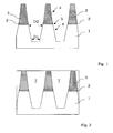
- Some known process steps to form these Flash memories, i.e. provided with a floating gate electrode, organised in matrix are shown in figures 1-5. In these figures some vertical section views are shown of the memory cells in a direction parallel to the "Word Lines", but in a different plane respect to this latter so as to highlight the evolution of the standard process flow in these areas.
- With reference to figure 1, on the
semiconductor substrate 1 insulation structures of the STI type are formed. - For example, on the semiconductor substrate 1 a
sacrificial oxide layer 2 and anitride layer 3 are formed in sequence. - On the nitride layer 3 a photolithographic mask provided with openings is then formed.
- Through the openings of the photolithographic mask, the
nitride layer 3 is etched so as to formfirst openings 4. The walls of theseopenings 4 are vertical or tapered downwards, i.e. the width of the vertical section of theopening 4 is not constant and it decreases approaching thesemiconductor substrate 1. - Through the
first openings 4 of thenitride layer 3, thesacrificial oxide layer 2 is then etched so as to formsecond openings 5. The walls of theseopenings 5 are vertical or tapered downwards. - Through the second openings of the
sacrificial oxide layer 2, surface portions of thesemiconductor substrate 1 are etched to formtrenches 6 in thesemiconductor substrate 1. The side walls of thetrenches 6 are tapered downwards of the device, i.e. the cross dimension D1 of the bottom wall of thetrench 6 is smaller with respect to the cross dimension D2 of the lower edge of thesecond openings 5 of thesacrificial oxide layer 2. - As shown in figure 2, an
oxide layer 7 called field oxide is then formed so as to fill in thetrenches 6, the first and thesecond openings - As shown in figure 3, the
nitride layer 3 and thesacrificial oxide layer 2 are completely removed.Superficial portions 7a of thefield oxide layer 7 then project from thesemiconductor substrate 1 and are divided from each other bythird openings 7b which have side walls being vertical with respect to the surface of thesemiconductor substrate 1 or these side walls diverge approaching thesemiconductor substrate 1. Thethird openings 7b have in fact the same shape as the one of thenitride layer 3 and of thesacrificial oxide layer 2 after the formation of the first andsecond openings surface portions 7a of thefield oxide layer 7 are vertical or tapered downwards i.e. their cross dimensions decrease approaching thesemiconductor substrate 1. In fact the walls of thesurface portions 7a of thefield oxide layer 7 follow the profile of the first andsecond openings field oxide layer 7 formed inside thesemiconductor substrate 1 follow the profile of thetrench 6. - A so called
tunnel oxide layer 8 is then formed on the exposed surface of thesemiconductor substrate 1. - As shown in figure 4, a
polysilicon layer 9 or amorphous silicon is then deposited on the whole device. - As it is well known polysilicon and amorphous silicon are conformal materials, i.e. they tend to follow the profile of the surface whereon they are deposited, therefore during the deposition step of the
polysilicon layer 9, if the aspect ratio (ratio between the height and the width) of thethird openings 7b is higher than 0.5:1, the deposition fronts formed on the side walls of thesurface portions 7a of thefield oxide layer 7, i.e. inside thethird openings 7b, touch each other before the deposition front formed on thetunnel layer 8 can completely fill in the space comprised betweenadjacent surface portions 7a of thefield oxide layer 7, thus formingvoids 10 inside thepolysilicon layer 9. - Therefore
voids 10 are formed inside the polysilicon layer any time the cross dimensions of thethird openings 7b are smaller than the double of their depth. - This drawback is also particularly evident when the side walls of the
third openings 7a have a cross section which widens approaching thesemiconductor substrate 1 as shown in figure 3. - The deposition of the
polysilicon layer 9 is continued until thesurface portions 7a of thefield oxide layer 7 are completely covered. - As shown in figure 5, a removal step of the
polysilicon layer 9 is made follow at least until thesurface portions 7a of thefield oxide layer 7 are expose. Portions of thepolysilicon layer 9 remaining confined between thesurface portions 7a of thefield oxide layer 7 form floatinggate electrodes 11 of the Flash memory cells having width W. - This removal step of the
polysilicon layer 9 is conventionally carried out by means of CMP (Chemical Mechanical Polishing). - The manufacturing process of the memory cells is then completed in a conventional way with the deposition, on the whole device, of an interpoly dielectric layer and a polysilicon layer for the formation of the control electrodes of the memory cells.
- As highlighted in figure 5, during the formation step of the
floating gate electrodes 11, thevoids 10 are uncovered and widened, therefore an imperfect interface surface is formed with the successive interpoly dielectric layer deposited on thefloating gate electrodes 11. This conformation of the floatinggate electrodes 11 can thus generate retention problems of the electric charge of the final Flash memory cell, altering its operation. - However, it is quite difficult to modify the shape of the first and
second openings trenches 6 acting on the process steps leading to the formation of these structures, so as to obtain improved profiles of the field oxide layer which allow a uniform filling of the floating gate electrodes. - The technical problem underlying the present invention is that of devising a method for forming non volatile memory cells, having such characteristics as to allow to avoid the formation of voids inside the floating gate electrodes overcoming the drawbacks still limiting the memory devices formed according to the prior art.
- The solution idea underlying the present invention is that of reducing the cross dimensions of the insulation regions insulating the floating gate electrodes of the memory cells from each other.
- On the basis of this solution idea the technical problem is solved by a method as previously indicated and defined in the characterising part of
claim 1. - The characteristics and the advantages of the method according to the invention will be apparent from the following description of an embodiment thereof given by way of indicative and non limiting example with reference to the annexed drawings.
- In these drawings:
- figures 1 to 5 show section views of a semiconductor substrate portion during the conventional manufacturing steps of a memory device;
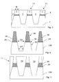
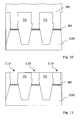
- figures 6 to 11 show section views of a semiconductor substrate portion during some manufacturing steps of a memory device according to the present invention.
- With reference to figures 6 to 11, a method is described for manufacturing non volatile memory cells integrated on a semiconductor substrate, each memory cell comprising a floating gate electrode.
- Advantageously, these non-volatile memory cells are comprised in memory electronic devices of the Flash type and organised in matrix; i.e. the cells are organised in rows, called word lines, and columns, called bit lines.
- For simplicity of description, figures 6 to 11 show vertical section views of these cells in a parallel direction "Word Lines" of a memory matrix wherein they can be integrated, but in a different plane respect to this latter so as to highlight the evolution of the standard process flow in these areas.
- In particular, with reference to figure 6, on the
semiconductor substrate 100 insulation structures of the STI type are formed. - On the semiconductor substrate 100 a sacrificial
dielectric layer 20, for example of sacrificial oxide, and aprotection layer 30, for example of nitride, are formed in sequence. - Nothing forbids that the sacrificial
dielectric layer 20 is not formed on thesemiconductor substrate 100. - On the protection layer 30 a photolithographic mask provided with openings is then formed.
- Through the openings of the photolithographic mask, the
protection layer 30 is etched so as to formfirst openings 40 whose walls are tapered downwards i.e. the width of the vertical section of eachsingle opening 40 is not constant and it decreases approaching thesemiconductor substrate 100. - Through the
first openings 40 of theprotection layer 30, thedielectric layer 20 is then etched so as to formsecond openings 50 whose walls are tapered downwards. - Through the
second openings 50 of thedielectric layer 20, surface portions of thesemiconductor substrate 100 are etched to formtrenches 60 in thesemiconductor substrate 100. Also the side walls of thetrenches 60 are tapered downwards of the device, i.e. the cross dimension D3 of the bottom wall of thetrench 60 is smaller with respect to the cross dimension D4 of the lower edge of thesecond openings 50 of thedielectric layer 20. - Although in the annexed figures the side walls are represented as perfectly rectilinear, these walls can also show a slight concavity or convexity, as well an irregular profile for example step-like.
- An
insulation layer 70, for example of field oxide, is then formed so as to fill in thetrenches 60, the first and thesecond openings - According to the invention, as shown in figure 7, the
protection layer 30 is only partially etched so thatsurface portions 71 of theinsulation layer 70, project from thesemiconductor substrate 1 separated from each other bythird openings 72 andlower portions 31 of theprotection layer 30 remain confined between thesurface portions 71 of theinsulation layer 70, below thethird openings 72. - Also the bottom walls of the
surface portions 71 of theinsulation layer 70 are tapered downwards i.e. their cross dimensions decrease approaching thesemiconductor substrate 100. - In particular, the etching step wherein the
protection layer 30 is partially removed is very selective with respect to theinsulation layer 70. - Advantageously, if the
protection layer 30 is formed by one nitride layer, the etching step of thislayer 30 comprises a solution of phosphoric acid (H3PO4). - Still according to the invention, as shown in figure 8, an etching step of the
insulation layer 70 is carried out. This etching step is very selective with respect to thelower portions 31 of theprotection layer 30 for which the cross dimensions of thesurface portions 71 of theinsulation layer 70 are reduced with consequent increase of the cross dimensions of thethird openings 72. It thus follows that thesurface portions 71 of theinsulation layer 70 are pulled back with respect to their initial position, in the direction indicated by the arrows in figure 8. - Clearly, in this etching step of the
insulation layer 70 also surface portions of theinsulation layer 70 are removed. - In particular, after this etching step of the
insulation layer 70, the side walls of thethird openings 72 between thesurface portions 71 of theinsulation layer 70 are at least vertical. - Advantageously, the side walls of the
openings 72 are tapered downwards, i.e. the cross dimensions of theopenings 72 decrease approaching thesemiconductor substrate 100. - Advantageously, this etching step if of the isotropic type for example of the wet type.
- Advantageously, if the
protection layer 30 is formed by one nitride layer the etching step of this layer comprises a solution of hydrofluoric acid (HF). - The
lower portions 31 of theprotection layer 30 are then completely removed together with thedielectric layer 20 so as to expose portions of thesemiconductor substrate 100. - A
further dielectric layer 80, for example of tunnel oxide, is then formed on the exposed surface of thesemiconductor substrate 100. - As shown in figure 10, a
conductive layer 90, for example of polysilicon, is then formed on the whole device. - According to the invention, the
polysilicon layer 90 completely fills in thethird openings 72 without forming voids due to the profile of thethird openings 72 which is vertical or tapered downwards. - In particular, if the side walls of the
third openings 72 are tapered downwards, it is easier for theconductive layer 90 to fill in the third openings without forming voids as it occurs in the prior art. - The formation step of the
polysilicon layer 90 is continued until thesurface portions 71 of theinsulation layer 70 are completely covered. - As shown in figure 11, a removal step of the
polysilicon layer 90 is made follow at least until thesurface portions 71 of theinsulation layer 70 are exposed, but it can also remove surface layers of the insulation layer. The portions of thepolysilicon layer 90 remaining confined between thesurface portions 71 of theinsulation layer 70 form floatinggate electrodes 110 of the Flash memory cells having width W. - This removal step of the
polysilicon layer 90 is conventionally carried out by means of CMP (Chemical Mechanical Polishing). - The process is then completed in a conventional way with the deposition, on the whole device, of an interpoly dielectric layer and a polysilicon layer for the formation of the control electrodes of the memory cells.
- In conclusion, the method according to the invention allows to form Flash memory cells without voids inside the floating gate electrodes, adding, to the conventional process flow, only two process steps which can be formed at low cost, without using to thermal treatments which could alter the thermal budget of the conventional manufacturing process and thus damage the
tunnel oxide layer 80 of the cells, and without intervening on the manufacturing steps of thetrenches 60 which are quite critical and difficult to be modified. - Although in the present description specific reference has been made to memory cells of the Flash type, the method according to the present invention can be advantageously applied to non volatile memory cells provided with floating gate electrodes.
Claims (11)
- Method for manufacturing non volatile memory cells integrated on a semiconductor substrate (100), each one comprising a floating gate electrode (110), the method comprising the steps of:- depositing at least one protective layer (30) on said semiconductor substrate (100),- forming a first plurality of openings (40) in said protective layer (30),- etching said semiconductor substrate (100) through said first plurality of openings (40) so as to form a plurality of trenches (60),- filling in said plurality of trenches (60) and said first plurality of openings (40) by means of an insulation layer (70), and being characterised in that it comprises the following steps:- etching surface portions of said protective layer (30) to form:- surface portions (71) of said insulation layer (70) projecting from the semiconductor substrate (100) divided from each other by a second plurality of openings (72), and- lower portions (31) of said protection layer (30) confined below said second plurality of openings (72),- etching said insulation layer (70) to reduce the cross dimensions of said surface portions (71) of said insulation layer (70),- removing said lower portions (31) of said protection layer (30) until said semiconductor substrate (100) is exposed.
- Method according to claim 1 characterised in that it comprises the steps of:- forming an insulation layer (80) on said exposed semiconductor substrate (100),- forming a conductive layer (90) on the whole device, said conductive layer (90) filling in said second plurality of openings (72) so as to form said floating gate electrodes (110).
- Method according to claim 2 characterised in that said formation step of said conductive layer (90) comprises the steps of:- deposition of said conductive layer (90), said conductive layer (90) completely coating surface portions (71) of said insulation layer (70),- removing, by means of CMP, a surface portion of said conductive layer (90) so as to expose at least surface portions (71) of said insulation layer (70).
- Method according to claim 1 characterised in that said etching step of surface portions of said protective layer (30) forms said second plurality of openings (72) with vertical side walls.
- Method according to claim 1 characterised in that said etching step of surface portions of said protective layer (30) forms said second plurality of openings (72) with the side walls tapered downwards.
- Method according to claim 1 characterised in that a further dielectric layer (20) is formed on the semiconductor substrate (100) prior to the protective layer (30).
- Method according to claim 6 characterised in that before forming said plurality of trenches (60), said further dielectric layer (20) is etched through said first plurality of openings (40) to form a third plurality of openings (50).
- Method according to claim 1 characterised in that said protective layer (30) is formed by a material which is highly selective with respect to the one of said insulation layer (70).
- Method according to claim 1 characterised in that said protective layer (30) is formed by a nitride layer and said insulation layer (70) is formed by a field oxide layer.
- Method according to claim 9 characterised in that said etching step of surface portions of said nitride layer (30) is formed by means of a solution comprising phosphoric acid, and that said etching step of said field oxide layer is formed by means of a solution comprising hydrofluoric acid.
- Method according to claim 1 characterised in that said memory cells are organised in matrix in a non volatile memory electronic device.
Priority Applications (2)
| Application Number | Priority Date | Filing Date | Title |
|---|---|---|---|
| EP05425943A EP1804294A1 (en) | 2005-12-30 | 2005-12-30 | Method for manufacturing non volatile memory cells |
| US11/647,504 US20070202647A1 (en) | 2005-12-30 | 2006-12-27 | Method for manufacturing non volatile memory cells integrated on a semiconductor substrate |
Applications Claiming Priority (1)
| Application Number | Priority Date | Filing Date | Title |
|---|---|---|---|
| EP05425943A EP1804294A1 (en) | 2005-12-30 | 2005-12-30 | Method for manufacturing non volatile memory cells |
Publications (1)
| Publication Number | Publication Date |
|---|---|
| EP1804294A1 true EP1804294A1 (en) | 2007-07-04 |
Family
ID=36498957
Family Applications (1)
| Application Number | Title | Priority Date | Filing Date |
|---|---|---|---|
| EP05425943A Withdrawn EP1804294A1 (en) | 2005-12-30 | 2005-12-30 | Method for manufacturing non volatile memory cells |
Country Status (2)
| Country | Link |
|---|---|
| US (1) | US20070202647A1 (en) |
| EP (1) | EP1804294A1 (en) |
Families Citing this family (4)
| Publication number | Priority date | Publication date | Assignee | Title |
|---|---|---|---|---|
| US7948021B2 (en) * | 2007-04-27 | 2011-05-24 | Kabushiki Kaisha Toshiba | Semiconductor memory device and method of fabricating the same |
| CN104979172B (en) * | 2014-04-01 | 2018-10-30 | 北京兆易创新科技股份有限公司 | A kind of floating boom of flash memory and preparation method thereof of ETOX structures |
| CN114420702B (en) * | 2021-03-23 | 2025-03-28 | 长江存储科技有限责任公司 | Three-dimensional memory and preparation method thereof |
| CN114846604A (en) | 2021-03-23 | 2022-08-02 | 长江存储科技有限责任公司 | Three-dimensional NAND memory and manufacturing method thereof |
Citations (5)
| Publication number | Priority date | Publication date | Assignee | Title |
|---|---|---|---|---|
| GB2366911A (en) * | 2000-09-08 | 2002-03-20 | Samsung Electronics Co Ltd | EEPROM devices having isolation region self aligned to floating gate |
| US6555427B1 (en) * | 1999-08-31 | 2003-04-29 | Kabushiki Kaisha Toshiba | Non-volatile semiconductor memory device and manufacturing method thereof |
| US6649472B1 (en) * | 2002-08-02 | 2003-11-18 | Taiwan Semiconductor Manufacturing Company | Method of manufacturing a flash memory cell with high programming efficiency by coupling from floating gate to sidewall |
| US20040145007A1 (en) * | 2003-01-24 | 2004-07-29 | Renesas Technology Corp. | Non-volatile semiconductor memory device and method of fabricating the same |
| US6787842B1 (en) * | 2003-04-02 | 2004-09-07 | Taiwan Semiconductor Manufacturing Co., Ltd | Method for operating a stacked gate field effect transistor (FET) device |
Family Cites Families (4)
| Publication number | Priority date | Publication date | Assignee | Title |
|---|---|---|---|---|
| US6008079A (en) * | 1998-03-25 | 1999-12-28 | Texas Instruments-Acer Incorporated | Method for forming a high density shallow trench contactless nonvolatile memory |
| JP4237344B2 (en) * | 1998-09-29 | 2009-03-11 | 株式会社東芝 | Semiconductor device and manufacturing method thereof |
| JP4683685B2 (en) * | 2000-01-17 | 2011-05-18 | ルネサスエレクトロニクス株式会社 | Semiconductor device manufacturing method, flash memory manufacturing method, and static random access memory manufacturing method |
| JP3516918B2 (en) * | 2000-01-19 | 2004-04-05 | 株式会社日立国際電気 | Semiconductor device manufacturing method and semiconductor manufacturing apparatus |
-
2005
- 2005-12-30 EP EP05425943A patent/EP1804294A1/en not_active Withdrawn
-
2006
- 2006-12-27 US US11/647,504 patent/US20070202647A1/en not_active Abandoned
Patent Citations (5)
| Publication number | Priority date | Publication date | Assignee | Title |
|---|---|---|---|---|
| US6555427B1 (en) * | 1999-08-31 | 2003-04-29 | Kabushiki Kaisha Toshiba | Non-volatile semiconductor memory device and manufacturing method thereof |
| GB2366911A (en) * | 2000-09-08 | 2002-03-20 | Samsung Electronics Co Ltd | EEPROM devices having isolation region self aligned to floating gate |
| US6649472B1 (en) * | 2002-08-02 | 2003-11-18 | Taiwan Semiconductor Manufacturing Company | Method of manufacturing a flash memory cell with high programming efficiency by coupling from floating gate to sidewall |
| US20040145007A1 (en) * | 2003-01-24 | 2004-07-29 | Renesas Technology Corp. | Non-volatile semiconductor memory device and method of fabricating the same |
| US6787842B1 (en) * | 2003-04-02 | 2004-09-07 | Taiwan Semiconductor Manufacturing Co., Ltd | Method for operating a stacked gate field effect transistor (FET) device |
Also Published As
| Publication number | Publication date |
|---|---|
| US20070202647A1 (en) | 2007-08-30 |
Similar Documents
| Publication | Publication Date | Title |
|---|---|---|
| CN105122455B (en) | Nonvolatile memory cell with self-aligned floating gate and erase gate and method of manufacturing the same | |
| US8120100B2 (en) | Overlapping trench gate semiconductor device | |
| CN100490153C (en) | Semiconductor device and method of manufacturing the same | |
| KR101140057B1 (en) | Semiconductor device and method for manufacturing the same | |
| JP2012248823A (en) | Nonvolatile memory device and manufacturing method of the same | |
| KR20100088836A (en) | Method of manufacturing a semiconductor device | |
| JP2008533705A (en) | Fabrication of carrier substrate contacts to trench-isolated SOI integrated circuits with high voltage components | |
| CN112992908B (en) | Semiconductor device and method for manufacturing the same | |
| KR100764360B1 (en) | Semiconductor device and manufacturing method thereof | |
| US11424255B2 (en) | Semiconductor device and manufacturing method thereof | |
| KR101604199B1 (en) | Flash memory semiconductor device and method thereof | |
| KR20050021469A (en) | Field effect transistor, associated use, and associated production method | |
| US20200402923A1 (en) | Vertical memory devices | |
| KR100590220B1 (en) | Nonvolatile Memory Device and Manufacturing Method Thereof | |
| KR20070059732A (en) | Flash memory and manufacturing method thereof | |
| US20070202647A1 (en) | Method for manufacturing non volatile memory cells integrated on a semiconductor substrate | |
| KR100673007B1 (en) | Nonvolatile Semiconductor Memory Device and Manufacturing Method Thereof | |
| KR20060099876A (en) | Gate Forming Method of Semiconductor Device | |
| EP1218941B1 (en) | Non-volatile memory having high gate coupling capacitance | |
| JP2008034820A (en) | Nonvolatile memory device and manufacturing method thereof | |
| US8097506B2 (en) | Shallow trench isolation for a memory | |
| US5990536A (en) | Integrated circuit arrangement having at least two mutually insulated components, and method for its production | |
| KR100629695B1 (en) | Method for manufacturing a semiconductor device having a recess gate | |
| KR100946120B1 (en) | Semiconductor memory device and manufacturing method thereof | |
| CN101136374A (en) | Method for manufacturing nonvolatile memory |
Legal Events
| Date | Code | Title | Description |
|---|---|---|---|
| PUAI | Public reference made under article 153(3) epc to a published international application that has entered the european phase |
Free format text: ORIGINAL CODE: 0009012 |
|
| AK | Designated contracting states |
Kind code of ref document: A1 Designated state(s): AT BE BG CH CY CZ DE DK EE ES FI FR GB GR HU IE IS IT LI LT LU LV MC NL PL PT RO SE SI SK TR |
|
| AX | Request for extension of the european patent |
Extension state: AL BA HR MK YU |
|
| 17P | Request for examination filed |
Effective date: 20071221 |
|
| 17Q | First examination report despatched |
Effective date: 20080206 |
|
| AKX | Designation fees paid |
Designated state(s): DE FR GB IT |
|
| RAP1 | Party data changed (applicant data changed or rights of an application transferred) |
Owner name: STMICROELECTRONICS SRL |
|
| STAA | Information on the status of an ep patent application or granted ep patent |
Free format text: STATUS: THE APPLICATION IS DEEMED TO BE WITHDRAWN |
|
| 18D | Application deemed to be withdrawn |
Effective date: 20110607 |