EP1802187A2 - Printed circuit board and manufacturing method thereof - Google Patents
Printed circuit board and manufacturing method thereof Download PDFInfo
- Publication number
- EP1802187A2 EP1802187A2 EP06123432A EP06123432A EP1802187A2 EP 1802187 A2 EP1802187 A2 EP 1802187A2 EP 06123432 A EP06123432 A EP 06123432A EP 06123432 A EP06123432 A EP 06123432A EP 1802187 A2 EP1802187 A2 EP 1802187A2
- Authority
- EP
- European Patent Office
- Prior art keywords
- center
- additional
- conductive layer
- layer
- insulation layer
- Prior art date
- Legal status (The legal status is an assumption and is not a legal conclusion. Google has not performed a legal analysis and makes no representation as to the accuracy of the status listed.)
- Ceased
Links
Images

Classifications
-
- H—ELECTRICITY
- H05—ELECTRIC TECHNIQUES NOT OTHERWISE PROVIDED FOR
- H05K—PRINTED CIRCUITS; CASINGS OR CONSTRUCTIONAL DETAILS OF ELECTRIC APPARATUS; MANUFACTURE OF ASSEMBLAGES OF ELECTRICAL COMPONENTS
- H05K3/00—Apparatus or processes for manufacturing printed circuits
- H05K3/46—Manufacturing multilayer circuits
- H05K3/4611—Manufacturing multilayer circuits by laminating two or more circuit boards
- H05K3/4614—Manufacturing multilayer circuits by laminating two or more circuit boards the electrical connections between the circuit boards being made during lamination
- H05K3/4617—Manufacturing multilayer circuits by laminating two or more circuit boards the electrical connections between the circuit boards being made during lamination characterized by laminating only or mainly similar single-sided circuit boards
-
- H—ELECTRICITY
- H05—ELECTRIC TECHNIQUES NOT OTHERWISE PROVIDED FOR
- H05K—PRINTED CIRCUITS; CASINGS OR CONSTRUCTIONAL DETAILS OF ELECTRIC APPARATUS; MANUFACTURE OF ASSEMBLAGES OF ELECTRICAL COMPONENTS
- H05K1/00—Printed circuits
- H05K1/02—Details
- H05K1/11—Printed elements for providing electric connections to or between printed circuits
- H05K1/115—Via connections; Lands around holes or via connections
-
- H—ELECTRICITY
- H05—ELECTRIC TECHNIQUES NOT OTHERWISE PROVIDED FOR
- H05K—PRINTED CIRCUITS; CASINGS OR CONSTRUCTIONAL DETAILS OF ELECTRIC APPARATUS; MANUFACTURE OF ASSEMBLAGES OF ELECTRICAL COMPONENTS
- H05K2201/00—Indexing scheme relating to printed circuits covered by H05K1/00
- H05K2201/09—Shape and layout
- H05K2201/09209—Shape and layout details of conductors
- H05K2201/095—Conductive through-holes or vias
- H05K2201/09627—Special connections between adjacent vias, not for grounding vias
-
- H—ELECTRICITY
- H05—ELECTRIC TECHNIQUES NOT OTHERWISE PROVIDED FOR
- H05K—PRINTED CIRCUITS; CASINGS OR CONSTRUCTIONAL DETAILS OF ELECTRIC APPARATUS; MANUFACTURE OF ASSEMBLAGES OF ELECTRICAL COMPONENTS
- H05K2201/00—Indexing scheme relating to printed circuits covered by H05K1/00
- H05K2201/09—Shape and layout
- H05K2201/09209—Shape and layout details of conductors
- H05K2201/09654—Shape and layout details of conductors covering at least two types of conductors provided for in H05K2201/09218 - H05K2201/095
- H05K2201/0969—Apertured conductors
-
- H—ELECTRICITY
- H05—ELECTRIC TECHNIQUES NOT OTHERWISE PROVIDED FOR
- H05K—PRINTED CIRCUITS; CASINGS OR CONSTRUCTIONAL DETAILS OF ELECTRIC APPARATUS; MANUFACTURE OF ASSEMBLAGES OF ELECTRICAL COMPONENTS
- H05K2203/00—Indexing scheme relating to apparatus or processes for manufacturing printed circuits covered by H05K3/00
- H05K2203/05—Patterning and lithography; Masks; Details of resist
- H05K2203/0548—Masks
- H05K2203/0554—Metal used as mask for etching vias, e.g. by laser ablation
-
- H—ELECTRICITY
- H05—ELECTRIC TECHNIQUES NOT OTHERWISE PROVIDED FOR
- H05K—PRINTED CIRCUITS; CASINGS OR CONSTRUCTIONAL DETAILS OF ELECTRIC APPARATUS; MANUFACTURE OF ASSEMBLAGES OF ELECTRICAL COMPONENTS
- H05K2203/00—Indexing scheme relating to apparatus or processes for manufacturing printed circuits covered by H05K3/00
- H05K2203/07—Treatments involving liquids, e.g. plating, rinsing
- H05K2203/0703—Plating
- H05K2203/0733—Method for plating stud vias, i.e. massive vias formed by plating the bottom of a hole without plating on the walls
-
- H—ELECTRICITY
- H05—ELECTRIC TECHNIQUES NOT OTHERWISE PROVIDED FOR
- H05K—PRINTED CIRCUITS; CASINGS OR CONSTRUCTIONAL DETAILS OF ELECTRIC APPARATUS; MANUFACTURE OF ASSEMBLAGES OF ELECTRICAL COMPONENTS
- H05K3/00—Apparatus or processes for manufacturing printed circuits
- H05K3/40—Forming printed elements for providing electric connections to or between printed circuits
- H05K3/42—Plated through-holes or plated via connections
- H05K3/423—Plated through-holes or plated via connections characterised by electroplating method
-
- H—ELECTRICITY
- H05—ELECTRIC TECHNIQUES NOT OTHERWISE PROVIDED FOR
- H05K—PRINTED CIRCUITS; CASINGS OR CONSTRUCTIONAL DETAILS OF ELECTRIC APPARATUS; MANUFACTURE OF ASSEMBLAGES OF ELECTRICAL COMPONENTS
- H05K3/00—Apparatus or processes for manufacturing printed circuits
- H05K3/46—Manufacturing multilayer circuits
- H05K3/4602—Manufacturing multilayer circuits characterized by a special circuit board as base or central core whereon additional circuit layers are built or additional circuit boards are laminated
-
- H—ELECTRICITY
- H05—ELECTRIC TECHNIQUES NOT OTHERWISE PROVIDED FOR
- H05K—PRINTED CIRCUITS; CASINGS OR CONSTRUCTIONAL DETAILS OF ELECTRIC APPARATUS; MANUFACTURE OF ASSEMBLAGES OF ELECTRICAL COMPONENTS
- H05K3/00—Apparatus or processes for manufacturing printed circuits
- H05K3/46—Manufacturing multilayer circuits
- H05K3/4644—Manufacturing multilayer circuits by building the multilayer layer by layer, i.e. build-up multilayer circuits
- H05K3/4652—Adding a circuit layer by laminating a metal foil or a preformed metal foil pattern
Definitions
- the invention relates to a printed circuit board (PCB) and the manufacturing method thereof.
- PCB printed circuit board
- the manufacturing method thereof relates to a multi-layer PCB with shared conductive pads and the method of manufacturing the same.
- the PCB is a circuit board that supports electronic devices with a circuit design on an insulator, through the steps of patterning the circuit layout and specific machining and processing.
- the present invention is to let the onboard electronic devices function normally.
- FIG. 1A shows the cross-sectional view of a multi-layer PCB that is drilled through using a traditional drilling head.
- the connections between the layers are achieved by stacking several boards, followed by drilling holes through the stack at predetermined positions to form the vias 102, which are also called the plated through hole (PTH).
- PTH plated through hole
- plating is used to form a conductive film 104 on the wall of the via.
- the different layers are connected using pads 106 and conductive copper films 104. That is, the conventional multi-layer PCB is manufactured by a single pressing, followed by drilling, plating, and circuit etching.
- another conventional method of adding layers is to first form base vias 126 using conventional mechanical drilling for the base layers 120.
- the vias 124 of the outermost, i.e. the upper and lower, additional layers 122 are formed by laser drilling, before pressing them to the base layers 120.
- This forms a multi-layer structure with non-through holes.
- it is impossible to prevent unnecessary through holes from being produced on the base layers.
- Both the above-mentioned two production methods in the prior art use mechanical drilling.
- the diameter of the drilled holes are larger.
- the needed pad size also inevitably occupies a larger area on each layer.
- One aspect of the invention is to provide a PCB and the manufacturing method thereof for obtaining a smaller pad size than conventional mechanical drilling methods.
- Another aspect of the invention is to provide a PCB and the manufacturing method thereof for preventing unnecessary drilling and increasing the layout area.
- a further aspect of the invention is to provide a PCB and the manufacturing method thereof for achieving the pad design data sharing and effectively saving the layout time.
- the disclosed PCB manufacturing method includes: providing a conductive layer deposited on an insulation layer; patterning the conductive layer and forming at least one conductive layer opening; drilling at the conductive layer opening through the insulation layer and forming a via; introducing a conductive material in the via; and repeating the above-mentioned steps for forming a plurality of layers, and bonding the layers together.
- At least one conductive layer opening is located at a position normal to the board that is not perpendicular to its adjacent conductive layer opening.
- the copper clad laminate (CCL) is used as the material for each layer.
- the center substrate contains an insulation layer and two copper foils on the upper and lower sides thereof.
- a circuit is patterned on the center substrate and the copper foil layer of an additional substrate.
- a copper foil opening is formed at a predetermined via.
- a carbon dioxide laser drills a hole on the insulation layer at the copper foil opening, forming a via.
- the center substrate and the additional substrate are bonded together. The rest of the additional substrates are further bonded thereon as needed.
- Another embodiment of the invention is a PCB with a center substrate and at least one additional substrate.
- the center substrate has a center insulation layer connected to a center conductive layer.
- the center insulation layer has a center via.
- the additional substrate has an additional insulation layer and an additional conductive layer.
- the additional insulation layer is sandwiched between the center conductive layer and the additional conductive layer and has an additional via.
- the center via and the additional via are loaded with a conductive material.
- An axis of the center via and an axis of the additional via are separated by a predetermined distance and are electrically coupled via the additional conductive layer and the conductive material.
- a further embodiment of the invention is a portable electronic device comprising a display unit, a control unit, and an input unit.
- the control unit includes an arbitrary via circuit board structure of the invention.
- the disclosed circuit board is applied to a portable electronic device, such as a mobile phone.
- the via at an arbitrary position in the multi-layer structure can be formed using existing processes and equipment without any special arrangement. Therefore, this not only reduces the formation of unnecessary through holes, but increases the available layout area.
- the circuit design personnel does not need to produce a different file data for different processes based on the prior art.
- a design with file data sharing is used instead. That is, different PCB processes can share the PCB circuit layout file data and the layout file data format in order to avoid complications and satisfying many more electronic circuit design requirements.
- the invention discloses a PCB and the manufacturing method thereof. Its sharing pad design is suitable for different multi-layer circuit board processes. By drilling and bonding layer by layer, the invention achieves the goals of forming a through hole at an arbitrary position in the multi-layer structure and reducing unnecessary wasted space caused by the through hole.
- the disclosed PCB manufacturing method includes the following steps. First, a conductive layer deposited on an insulation layer is provided. The conductive layer is patterned and formed with at least one conductive layer opening. The conductive layer opening is drilled through the insulation layer, forming a via. The via is loaded with a conductive material. A plurality of substrates are formed using the above steps and bonded according to the design. At least one conductive layer opening is formed at a position along the normal to the board that is not perpendicular to its adjacent conductive layer opening.
- each layer uses a conventional CCL. That is, one or both surfaces of each insulation layer are covered with copper foils.
- the copper foil is the conductive layer to be patterned.
- the insulation layer contains phenolic or epoxy, called the resin substrate.
- a center insulation layer and a center copper foil layer are provided first.
- the center copper foil layer is a conductive layer that is bonded with the central insulation layer in advance.
- a desired circuit pattern is defined on the center copper foil layer. That is, the center copper foil layer is patterned according the circuit blueprint, forming a necessary circuit structure. The patterning includes forming at least one center copper foil opening. The center copper foil opening is used for forming the center via in the subsequent drilling step.
- the center copper foil opening is drilled through the center insulation layer, forming at least one center via.
- the drilling method can be conventional mechanical drilling or laser drilling, which can render an opening with a smaller diameter.
- the laser drilling may be done with a carbon dioxide laser.
- chemical plating fills the center via with a conductive material, preferably copper, thereby connecting layers.
- step 208 the center via is loaded with a conductive material to provide an electrical connection.
- a center substrate is obtained by electroplating or other deposition methods.
- step 210 a first additional substrate is prepared following the above-mentioned steps 202 to 208.
- step 212 the first additional substrate is bonded with the center substrate.
- the conducting circuit between the additional layer and the center layer follows a predetermined design.
- a circuit is patterned on the layer copper foil in the center. Additional substrates are prepared according to the design (step 210). The center substrate is then bonded with additional substrates to render a multi-layer PCB (step 212).
- the above describes an example of bonding the substrates layer by layer. However, one may also first prepare all the substrates and then bond them together all at once.
- the center substrate may already be one with multi-layer substrates. It can be mechanically drilled to form vias and electroplated and then bonded with additional substrates using the disclosed method.
- the invention is not restricted to the case where each layer of substrate has to be laser drilled to form individual vias, followed by electroplating and bonding. Such variations can be readily performed by a person skilled in the art.
- another embodiment of the invention is a PCB structure that contains a center substrate 300 and at least one additional substrate 310.
- the center substrate 300 contains a center insulation layer 302 connected to a center conductive layer 304b.
- the center insulation layer 302 has a center via 306.
- the additional substrate 320 contains an additional insulation layer 322 and an additional conductive layer 324.
- the additional insulation layer 322 is disposed between the center conductive layer 304b and the additional conductive layer 324.
- the additional insulation layer 322 has an additional via 326.
- the center via 306 and the additional via 326 are loaded with a conductive material 330.
- the axis 308 of the center via 308 and the axis 328 of the additional via are separated by a predetermined distance P. They are electrically coupled through the center conductive layer 304b and the conductive material 330.
- the circuit board is a PCB with eight layers of circuits. It includes a center substrate and six additional substrates.
- FIG. 3A or 3B clearly shows that the center substrate 300 includes a center insulation layer and two center conductive layers disposed and pre-bonded above and below the center insulation layer before further bonding.
- Each additional substrate 310 or 320 includes an additional insulation layer and an additional conductive layer.
- the conductive layer uses the copper foil in this embodiment.
- the center substrate 300 includes a center insulation layer 302, a first center conductive layer 304a and a second center conductive layer 304b.
- the first center conductive layer 304a is bonded to the lower surface of the center insulation layer 302.
- the second center conductive layer 304b is bonded to the upper surface of the center insulation layer 302.
- the center insulation layer 302 is formed with a center via 306.
- the two conductive layers are formed with predetermined circuits.
- each via is formed by laser drilling, the size of the pad 350 thereon may be as small as or smaller than approximately 10mm.
- Each via is formed with copper 330 by electroplating to achieve electrical conduction.
- the conductive material 330 inside the via can be formed using some other deposition method.
- a first additional layer 310 is bonded to the lower surface of the first center conductive layer 304a.
- the first additional layer 310 includes a first additional insulation layer 312 and a first additional conductive layer 314.
- the first additional insulation layer is disposed between the first center conductive layer 304a and the first additional conductive layer 314 and formed with a first additional via 316.
- the first additional via 316 and the center via 306 are at roughly at the same position along the normal to the board T. That is, the axis 318 of the first additional via 318 and the axis 308 of the center via are roughly the same. Therefore, if the via diameter requirement is not strict in this embodiment, the center substrate 300 and the first additional substrate 310 can be bonded first, followed by traditional mechanical drilling. There is no need to perform laser drilling individually before bonding them together.
- the second additional substrate 320 is bonded on the upper surface of the second center conductive layer 304b.
- the second additional substrate 320 includes a second additional insulation layer 322 and a second additional conductive layer 324.
- the second additional insulation layer 322 is disposed between the second center conductive layer 304b and the second additional conductive layer 324 and formed with a second additional via 326.
- the second additional via 326 and the center via 306 are at different positions along the normal to the board T. That is, the axis 328 of the second additional via and the axis 308 of the center via are separated by a predetermined distance P.
- each of the above-mentioned conductive layers is patterned first.
- the drawings have been simplified from the actual circuit board structure.
- Each insulation layer has only one via in them.
- each conductive layer only displays the pad and the related connection, emphasizing that the disclosed connection design does not need to be the same as in the prior art of drilling holes at the corresponding position on each substrate.
- the holes are formed only at specific, necessary layers. Therefore, the layout area on each layer is increased.
- FIG. 4 is a schematic view of the disclosed PCB in a portable electronic device, such as a mobile phone.
- the electronic device includes a display unit 430, a control unit 420, and an input unit.
- the control unit 420 includes the circuit board structure 400 with an arbitrary via according to the invention, e.g. the circuit board structure in FIG. 3B.
- the input unit 410 can be, for example, a key set for entering an input signal.
- the input signal is transmitted via the circuit board structure and processed by a device on the control unit 420, such as a chip (not shown).
- the display unit 430 can be, for example, a liquid crystal display (LCD) panel. An image responds to the input signal.
- LCD liquid crystal display
- the invention has the following advantages.
- the PCB is patterned according to a circuit layout. Before drilling holes in each layer of substrate, copper foil openings are patterned for subsequent hole drilling. Therefore, vias can be formed in the insulation layer by direct laser drilling, rendering small holes. This further reduces the size and cost of pads.
- the position of the via in each layer can be arbitrarily selected. It is not restricted to one drilling through all the substrates. The available layout area is also increased. Therefore, the invention provides a breakthrough in the technical development of device integration and miniaturization.
- the sizes of pads are different in various kinds of multi-layer manufacturing processes in the prior art.
- the circuit designer has to produce different data files for different processes using, for example, the commonly seen layout file format.
- the invention can be implemented using existing processes without employing any other special process. It can be applied to soft, hard, and combined PCB's. With the shared data file, the pads on the circuit board can be shared by different processes, satisfying the requirements of different PCB manufacturing processes. It effectively saves the circuit layout time. As the manpower and materials are efficiently used in the invention, the total cost is largely reduced.
Landscapes
- Engineering & Computer Science (AREA)
- Microelectronics & Electronic Packaging (AREA)
- Manufacturing & Machinery (AREA)
- Production Of Multi-Layered Print Wiring Board (AREA)
- Printing Elements For Providing Electric Connections Between Printed Circuits (AREA)
Abstract
Description
- The invention relates to a printed circuit board (PCB) and the manufacturing method thereof. In particular, it relates to a multi-layer PCB with shared conductive pads and the method of manufacturing the same.
- The PCB is a circuit board that supports electronic devices with a circuit design on an insulator, through the steps of patterning the circuit layout and specific machining and processing. The present invention is to let the onboard electronic devices function normally.
- In the existing multi-layer PCB manufacturing process, vias are created using different methods. For example, the layers of the PCB can be mechanically drilled all at once. That is, the holes are formed by drilling through the resin layers, such as the phenolic or epoxy, along with copper foils. FIG. 1A shows the cross-sectional view of a multi-layer PCB that is drilled through using a traditional drilling head. In the drawing, the connections between the layers are achieved by stacking several boards, followed by drilling holes through the stack at predetermined positions to form the
vias 102, which are also called the plated through hole (PTH). Afterwards, plating is used to form aconductive film 104 on the wall of the via. The different layers are connected usingpads 106 andconductive copper films 104. That is, the conventional multi-layer PCB is manufactured by a single pressing, followed by drilling, plating, and circuit etching. - As shown in FIG. 1B, another conventional method of adding layers is to first
form base vias 126 using conventional mechanical drilling for thebase layers 120. Thevias 124 of the outermost, i.e. the upper and lower,additional layers 122 are formed by laser drilling, before pressing them to thebase layers 120. This forms a multi-layer structure with non-through holes. However, it is impossible to prevent unnecessary through holes from being produced on the base layers. Both the above-mentioned two production methods in the prior art use mechanical drilling. The diameter of the drilled holesare larger. The needed pad size also inevitably occupies a larger area on each layer. - In view of the miniaturization trend of electronic products, efficient use of the limited PCB layer area is an important technical issue. If the diameters cannot be decreased, the layout space on the board will become very restricted. One-time drilling to form a through hole in all the stacked boards is also a cost in the configuration of the pads. This is because each board layer has to be provided with a pad in order to connect different layers. However, unless several layers should be connected with one another, the drilling through method wastes circuit space in other layers and results in signal interference.
- One aspect of the invention is to provide a PCB and the manufacturing method thereof for obtaining a smaller pad size than conventional mechanical drilling methods.
- Another aspect of the invention is to provide a PCB and the manufacturing method thereof for preventing unnecessary drilling and increasing the layout area.
- A further aspect of the invention is to provide a PCB and the manufacturing method thereof for achieving the pad design data sharing and effectively saving the layout time.
- In accord with the above aspects, the disclosed PCB manufacturing method includes: providing a conductive layer deposited on an insulation layer; patterning the conductive layer and forming at least one conductive layer opening; drilling at the conductive layer opening through the insulation layer and forming a via; introducing a conductive material in the via; and repeating the above-mentioned steps for forming a plurality of layers, and bonding the layers together. At least one conductive layer opening is located at a position normal to the board that is not perpendicular to its adjacent conductive layer opening.
- According to a preferred embodiment of the invention, the copper clad laminate (CCL) is used as the material for each layer. The center substrate contains an insulation layer and two copper foils on the upper and lower sides thereof. A circuit is patterned on the center substrate and the copper foil layer of an additional substrate. A copper foil opening is formed at a predetermined via. A carbon dioxide laser drills a hole on the insulation layer at the copper foil opening, forming a via. Finally, the center substrate and the additional substrate are bonded together. The rest of the additional substrates are further bonded thereon as needed.
- Another embodiment of the invention is a PCB with a center substrate and at least one additional substrate. The center substrate has a center insulation layer connected to a center conductive layer. The center insulation layer has a center via. The additional substrate has an additional insulation layer and an additional conductive layer. The additional insulation layer is sandwiched between the center conductive layer and the additional conductive layer and has an additional via. The center via and the additional via are loaded with a conductive material. An axis of the center via and an axis of the additional via are separated by a predetermined distance and are electrically coupled via the additional conductive layer and the conductive material.
- A further embodiment of the invention is a portable electronic device comprising a display unit, a control unit, and an input unit. The control unit includes an arbitrary via circuit board structure of the invention. The disclosed circuit board is applied to a portable electronic device, such as a mobile phone.
- According to the disclosed manufacturing method of the PCB, the via at an arbitrary position in the multi-layer structure can be formed using existing processes and equipment without any special arrangement. Therefore, this not only reduces the formation of unnecessary through holes, but increases the available layout area. The circuit design personnel does not need to produce a different file data for different processes based on the prior art. A design with file data sharing is used instead. That is, different PCB processes can share the PCB circuit layout file data and the layout file data format in order to avoid complications and satisfying many more electronic circuit design requirements.
- These and other features, aspects and advantages of the invention will become apparent by reference to the following description and accompanying drawings which are given by way of illustration only, and thus are not limitative of the invention, and wherein:
- FIG. 1A is a schematic cross-sectional view of the circuit board structure formed using conventional mechanical drilling;
- FIG. 1B is a schematic cross-sectional view of the circuit board structure formed using the conventional layer addition method;
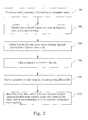
- FIG. 2 is a flowchart of the PCB manufacturing method according to a preferred embodiment of the invention;
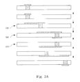
- FIG. 3A is a schematic cross-sectional view of the layers of substrates before bonding in a preferred embodiment of the invention;
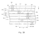
- FIG. 3B is a schematic cross-sectional view of the layers of substrates after bonding in the preferred embodiment of the invention; and
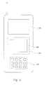
- FIG. 4 is a schematic view of using the disclosed PCB in a portable electronic device.
- The present invention will be apparent from the following detailed description, which proceeds with reference to the accompanying drawings, wherein the same references relate to the same elements.
- The invention discloses a PCB and the manufacturing method thereof. Its sharing pad design is suitable for different multi-layer circuit board processes. By drilling and bonding layer by layer, the invention achieves the goals of forming a through hole at an arbitrary position in the multi-layer structure and reducing unnecessary wasted space caused by the through hole.
- With reference to FIG. 2, the disclosed PCB manufacturing method includes the following steps. First, a conductive layer deposited on an insulation layer is provided. The conductive layer is patterned and formed with at least one conductive layer opening. The conductive layer opening is drilled through the insulation layer, forming a via. The via is loaded with a conductive material. A plurality of substrates are formed using the above steps and bonded according to the design. At least one conductive layer opening is formed at a position along the normal to the board that is not perpendicular to its adjacent conductive layer opening.
- In this embodiment, each layer uses a conventional CCL. That is, one or both surfaces of each insulation layer are covered with copper foils. The copper foil is the conductive layer to be patterned. The insulation layer contains phenolic or epoxy, called the resin substrate. In
step 202, a center insulation layer and a center copper foil layer are provided first. The center copper foil layer is a conductive layer that is bonded with the central insulation layer in advance. - In
step 204, a desired circuit pattern is defined on the center copper foil layer. That is, the center copper foil layer is patterned according the circuit blueprint, forming a necessary circuit structure. The patterning includes forming at least one center copper foil opening. The center copper foil opening is used for forming the center via in the subsequent drilling step. - In
step 206, the center copper foil opening is drilled through the center insulation layer, forming at least one center via. The drilling method can be conventional mechanical drilling or laser drilling, which can render an opening with a smaller diameter. The laser drilling may be done with a carbon dioxide laser. Afterwards, chemical plating fills the center via with a conductive material, preferably copper, thereby connecting layers. - In
step 208, the center via is loaded with a conductive material to provide an electrical connection. Finally, a center substrate is obtained by electroplating or other deposition methods. Instep 210, a first additional substrate is prepared following the above-mentionedsteps 202 to 208. Instep 212, the first additional substrate is bonded with the center substrate. - In this embodiment, the conducting circuit between the additional layer and the center layer follows a predetermined design. When preparing the center substrate, a circuit is patterned on the layer copper foil in the center. Additional substrates are prepared according to the design (step 210). The center substrate is then bonded with additional substrates to render a multi-layer PCB (step 212).
- The above describes an example of bonding the substrates layer by layer. However, one may also first prepare all the substrates and then bond them together all at once. Although the above-mentioned manufacturing procedure is described for only one center substrate and one additional substrate, the center substrate may already be one with multi-layer substrates. It can be mechanically drilled to form vias and electroplated and then bonded with additional substrates using the disclosed method. The invention is not restricted to the case where each layer of substrate has to be laser drilled to form individual vias, followed by electroplating and bonding. Such variations can be readily performed by a person skilled in the art.
- With simultaneous reference to FIGS. 3A and 3B, another embodiment of the invention is a PCB structure that contains a
center substrate 300 and at least oneadditional substrate 310. Thecenter substrate 300 contains acenter insulation layer 302 connected to a centerconductive layer 304b. Thecenter insulation layer 302 has a center via 306. - The
additional substrate 320 contains anadditional insulation layer 322 and an additionalconductive layer 324. Theadditional insulation layer 322 is disposed between the centerconductive layer 304b and the additionalconductive layer 324. Theadditional insulation layer 322 has an additional via 326. The center via 306 and the additional via 326 are loaded with aconductive material 330. The axis 308 of the center via 308 and theaxis 328 of the additional via are separated by a predetermined distance P. They are electrically coupled through the centerconductive layer 304b and theconductive material 330. - In a preferred embodiment, the circuit board is a PCB with eight layers of circuits. It includes a center substrate and six additional substrates. FIG. 3A or 3B clearly shows that the
center substrate 300 includes a center insulation layer and two center conductive layers disposed and pre-bonded above and below the center insulation layer before further bonding. Eachadditional substrate - The
center substrate 300 includes acenter insulation layer 302, a first centerconductive layer 304a and a second centerconductive layer 304b. The first centerconductive layer 304a is bonded to the lower surface of thecenter insulation layer 302. The second centerconductive layer 304b is bonded to the upper surface of thecenter insulation layer 302. Thecenter insulation layer 302 is formed with a center via 306. The two conductive layers are formed with predetermined circuits. - If each via is formed by laser drilling, the size of the
pad 350 thereon may be as small as or smaller than approximately 10mm. Each via is formed withcopper 330 by electroplating to achieve electrical conduction. Theconductive material 330 inside the via can be formed using some other deposition method. - A first
additional layer 310 is bonded to the lower surface of the first centerconductive layer 304a. The firstadditional layer 310 includes a firstadditional insulation layer 312 and a first additionalconductive layer 314. The first additional insulation layer is disposed between the first centerconductive layer 304a and the first additionalconductive layer 314 and formed with a first additional via 316. - The first additional via 316 and the center via 306 are at roughly at the same position along the normal to the board T. That is, the
axis 318 of the first additional via 318 and the axis 308 of the center via are roughly the same. Therefore, if the via diameter requirement is not strict in this embodiment, thecenter substrate 300 and the firstadditional substrate 310 can be bonded first, followed by traditional mechanical drilling. There is no need to perform laser drilling individually before bonding them together. - The second
additional substrate 320 is bonded on the upper surface of the second centerconductive layer 304b. The secondadditional substrate 320 includes a secondadditional insulation layer 322 and a second additionalconductive layer 324. The secondadditional insulation layer 322 is disposed between the second centerconductive layer 304b and the second additionalconductive layer 324 and formed with a second additional via 326. The second additional via 326 and the center via 306 are at different positions along the normal to the board T. That is, theaxis 328 of the second additional via and the axis 308 of the center via are separated by a predetermined distance P. - Each of the above-mentioned conductive layers is patterned first. The drawings have been simplified from the actual circuit board structure. Each insulation layer has only one via in them. Moreover, each conductive layer only displays the pad and the related connection, emphasizing that the disclosed connection design does not need to be the same as in the prior art of drilling holes at the corresponding position on each substrate. The holes are formed only at specific, necessary layers. Therefore, the layout area on each layer is increased.
- FIG. 4 is a schematic view of the disclosed PCB in a portable electronic device, such as a mobile phone. The electronic device includes a
display unit 430, acontrol unit 420, and an input unit. Thecontrol unit 420 includes thecircuit board structure 400 with an arbitrary via according to the invention, e.g. the circuit board structure in FIG. 3B. - The
input unit 410 can be, for example, a key set for entering an input signal. The input signal is transmitted via the circuit board structure and processed by a device on thecontrol unit 420, such as a chip (not shown). Thedisplay unit 430 can be, for example, a liquid crystal display (LCD) panel. An image responds to the input signal. It should be noted that the circuit layout of the arbitrary viacircuit board 400 and the devices thereon have not be shown in order to emphasize the characteristic of an arbitrary via position in the invention. - According to the above-mentioned preferred embodiment, the invention has the following advantages. The PCB is patterned according to a circuit layout. Before drilling holes in each layer of substrate, copper foil openings are patterned for subsequent hole drilling. Therefore, vias can be formed in the insulation layer by direct laser drilling, rendering small holes. This further reduces the size and cost of pads.
- According to the invention, the position of the via in each layer can be arbitrarily selected. It is not restricted to one drilling through all the substrates. The available layout area is also increased. Therefore, the invention provides a breakthrough in the technical development of device integration and miniaturization.
- Besides, the sizes of pads are different in various kinds of multi-layer manufacturing processes in the prior art. The circuit designer has to produce different data files for different processes using, for example, the commonly seen layout file format. The invention can be implemented using existing processes without employing any other special process. It can be applied to soft, hard, and combined PCB's. With the shared data file, the pads on the circuit board can be shared by different processes, satisfying the requirements of different PCB manufacturing processes. It effectively saves the circuit layout time. As the manpower and materials are efficiently used in the invention, the total cost is largely reduced.
- The invention being thus described, it will be obvious that the same may be varied in many ways. Such variations are not to be regarded as a departure from the spirit and scope of the invention, and all such modifications as would be obvious to one skilled in the art are intended to be included within the scope of the following claims.
Claims (10)
- A manufacturing method of a multi-layer circuit board comprising the following steps:(g) providing a conductive layer disposed on an insulation layer;(h) patterning the conductive layer and forming at least one conductive layer opening;(i) drilling a hole at the conductive layer opening through the insulation layer, thereby forming a via;(j) introducing a conductive material in the via;(k) forming a plurality of substrates by repeating steps (g) to (j); and(l) bonding the substrates;wherein at least one conductive layer opening located at the position along a normal direction to the board that is not perpendicular to its adjacent conductive layer opening.
- The method of claim 1, wherein the bonding step is performed immediately after the substrate is formed or after all the substrates are formed.
- The method of claim 1, wherein the drilling step involves laser drilling or mechanical drilling.
- The method of claim 1, wherein the step of introducing a conductive material in the via is performed by electroplating or deposition.
- A printed circuit board (PCB), comprising:a center substrate having a center insulation layer connected to a center conductive layer, the center insulation layer having a center via; andan additional substrate having an additional insulation layer and an additional conductive layer, the additional insulation layer being disposed between the center conductive layer and the additional conductive layer and having an additional via;wherein the center via and the additional via are loaded with a conductive material, the axis of the center via and the axis of the additional via are separated by a predetermined distance and electrically coupled using the center conductive layer and the conductive material.
- The PCB of claim 5, wherein the center substrate has a multi-layer substrate structure.
- The PCB of claim 5, wherein the material of the insulation layer includes phenolic resin or epoxy resin.
- The PCB of claim 5, wherein the conductive material is loaded in the center via and/or the additional via by electroplating or deposition.
- A multi-layer PCB comprising:a center substrate having a center insulation layer with a center via and disposed between a center conductive layer and a second center conductive layer;a first additional substrate having a first additional insulation layer with a first additional via and disposed between the first center conductive layer and the first additional conductive layer; anda second additional substrate having a second additional insulation layer with a second additional via and disposed between the second center conductive layer and the second additional conductive layer;wherein the center via and the additional vias are loaded with a conductive material, the axis of the center via is separated from the axis of the second additional via by a predetermined distance and coincides with the axis of the first additional via along the normal to the board, and the center via and the additional vias are electrically coupled using the center conductive layer and the conductive material.
- A portable electronic device comprising:an input unit for entering an input signal;a control unit, which includes:wherein the center via and the additional via are loaded with a conductive material, the axis of the center via and the axis of the additional via are separated by a predetermined distance and are electrically coupled using the center conductive layer and the conductive material, and the input signal is transmitted between the substrates; anda center substrate having a center insulation layer connected to a center conductive layer, the center insulation layer having a center via; andan additional substrate having an additional insulation layer and an additional conductive layer, the additional insulation layer being disposed between the center conductive layer and the additional conductive layer and having an additional via;
a display unit, which responds with an image corresponding to the input signal.
Applications Claiming Priority (1)
| Application Number | Priority Date | Filing Date | Title |
|---|---|---|---|
| CNA2005100035942A CN1993018A (en) | 2005-12-26 | 2005-12-26 | Printed circuit board and manufacturing method thereof |
Publications (2)
| Publication Number | Publication Date |
|---|---|
| EP1802187A2 true EP1802187A2 (en) | 2007-06-27 |
| EP1802187A3 EP1802187A3 (en) | 2008-01-23 |
Family
ID=38001766
Family Applications (1)
| Application Number | Title | Priority Date | Filing Date |
|---|---|---|---|
| EP06123432A Ceased EP1802187A3 (en) | 2005-12-26 | 2006-11-03 | Printed circuit board and manufacturing method thereof |
Country Status (2)
| Country | Link |
|---|---|
| EP (1) | EP1802187A3 (en) |
| CN (1) | CN1993018A (en) |
Cited By (4)
| Publication number | Priority date | Publication date | Assignee | Title |
|---|---|---|---|---|
| FR2969897A1 (en) * | 2010-12-23 | 2012-06-29 | Thales Sa | Multilayer printed circuit for e.g. ultra high frequency circuit, has electrical contacts compressed according to stacking direction between plated through-holes and complementary elements |
| WO2017156678A1 (en) * | 2016-03-14 | 2017-09-21 | 深圳崇达多层线路板有限公司 | Method for manufacturing stacked holes of circuit board |
| EP2718939B1 (en) * | 2011-06-08 | 2017-10-18 | Siemens Energy, Inc. | Insulation materials having apertures formed therein |
| CN111836464A (en) * | 2020-08-11 | 2020-10-27 | 日月光半导体(上海)有限公司 | Integrated circuit substrate and integrated circuit substrate manufacturing method |
Families Citing this family (3)
| Publication number | Priority date | Publication date | Assignee | Title |
|---|---|---|---|---|
| CN102595799B (en) * | 2011-12-30 | 2015-03-25 | 柏承科技(昆山)股份有限公司 | Manufacturing method of high-density interconnected printed circuit board |
| CN105934085A (en) * | 2016-06-28 | 2016-09-07 | 广东欧珀移动通信有限公司 | PCB board and mobile terminal with it |
| CN106793524A (en) * | 2017-02-10 | 2017-05-31 | 昆山元茂电子科技有限公司 | The manufacture method of printed circuit board (PCB) |
Family Cites Families (8)
| Publication number | Priority date | Publication date | Assignee | Title |
|---|---|---|---|---|
| JP3311899B2 (en) * | 1995-01-20 | 2002-08-05 | 松下電器産業株式会社 | Circuit board and method of manufacturing the same |
| JPH09116273A (en) * | 1995-08-11 | 1997-05-02 | Shinko Electric Ind Co Ltd | Multilayer circuit board and method of manufacturing the same |
| US6207259B1 (en) * | 1998-11-02 | 2001-03-27 | Kyocera Corporation | Wiring board |
| JP3760771B2 (en) * | 2001-01-16 | 2006-03-29 | 松下電器産業株式会社 | Circuit forming substrate and method of manufacturing circuit forming substrate |
| US6831236B2 (en) * | 2001-03-23 | 2004-12-14 | Fujikura Ltd. | Multilayer wiring board assembly, multilayer wiring board assembly component and method of manufacture thereof |
| JP3826731B2 (en) * | 2001-05-07 | 2006-09-27 | ソニー株式会社 | Multilayer printed wiring board and method for manufacturing multilayer printed wiring board |
| JP4199198B2 (en) * | 2003-01-16 | 2008-12-17 | 富士通株式会社 | Multilayer wiring board and manufacturing method thereof |
| US7211289B2 (en) * | 2003-12-18 | 2007-05-01 | Endicott Interconnect Technologies, Inc. | Method of making multilayered printed circuit board with filled conductive holes |
-
2005
- 2005-12-26 CN CNA2005100035942A patent/CN1993018A/en active Pending
-
2006
- 2006-11-03 EP EP06123432A patent/EP1802187A3/en not_active Ceased
Cited By (4)
| Publication number | Priority date | Publication date | Assignee | Title |
|---|---|---|---|---|
| FR2969897A1 (en) * | 2010-12-23 | 2012-06-29 | Thales Sa | Multilayer printed circuit for e.g. ultra high frequency circuit, has electrical contacts compressed according to stacking direction between plated through-holes and complementary elements |
| EP2718939B1 (en) * | 2011-06-08 | 2017-10-18 | Siemens Energy, Inc. | Insulation materials having apertures formed therein |
| WO2017156678A1 (en) * | 2016-03-14 | 2017-09-21 | 深圳崇达多层线路板有限公司 | Method for manufacturing stacked holes of circuit board |
| CN111836464A (en) * | 2020-08-11 | 2020-10-27 | 日月光半导体(上海)有限公司 | Integrated circuit substrate and integrated circuit substrate manufacturing method |
Also Published As
| Publication number | Publication date |
|---|---|
| EP1802187A3 (en) | 2008-01-23 |
| CN1993018A (en) | 2007-07-04 |
Similar Documents
| Publication | Publication Date | Title |
|---|---|---|
| JP4538486B2 (en) | Multilayer substrate and manufacturing method thereof | |
| CN104883807B (en) | Embedded board and its manufacturing method | |
| US7457129B2 (en) | Multilayer printed wiring board | |
| US10064292B2 (en) | Recessed cavity in printed circuit board protected by LPI | |
| KR20030057284A (en) | Multi-layered printed wiring board having via holes, circuit module comprising circuit elements mounted on the multi-layered printed wiring board, and method of manufacturing the multi-layered printed wiring board | |
| CN102387672A (en) | Method for manufacturing multilayer circuit board | |
| US20110005071A1 (en) | Printed Circuit Board and Manufacturing Method Thereof | |
| US10219374B2 (en) | Printed wiring board | |
| US10772220B2 (en) | Dummy core restrict resin process and structure | |
| US20170271734A1 (en) | Embedded cavity in printed circuit board by solder mask dam | |
| CN111182733A (en) | Circuit board manufacturing process with side wall circuit and circuit board manufacturing process | |
| CN1993018A (en) | Printed circuit board and manufacturing method thereof | |
| JPH10261854A (en) | Printed wiring board and manufacturing method thereof | |
| TWI706702B (en) | Via structures in the circuit board and fabrication methods thereof | |
| JP4485975B2 (en) | Manufacturing method of multilayer flexible circuit wiring board | |
| JP4347143B2 (en) | Circuit board and manufacturing method thereof | |
| CN101351091A (en) | Circuit connection process and structure thereof | |
| US20040182603A1 (en) | [inner layer structure of a circuit board] | |
| KR20030071391A (en) | Method for creating bump and making printed circuit board using the said bump | |
| KR20070056188A (en) | Manufacturing method of cavity type printed circuit board | |
| JP4397793B2 (en) | Circuit board and manufacturing method thereof | |
| JPH06350256A (en) | Printed wiring board having non-through hole and production of thereof | |
| JPH08111584A (en) | Method for manufacturing sheet laminated multilayer wiring board | |
| KR20030078449A (en) | Method for creating bump and making printed circuit board using the said bump | |
| JPH11298148A (en) | IVH substrate and method of manufacturing the same |
Legal Events
| Date | Code | Title | Description |
|---|---|---|---|
| PUAI | Public reference made under article 153(3) epc to a published international application that has entered the european phase |
Free format text: ORIGINAL CODE: 0009012 |
|
| AK | Designated contracting states |
Kind code of ref document: A2 Designated state(s): AT BE BG CH CY CZ DE DK EE ES FI FR GB GR HU IE IS IT LI LT LU LV MC NL PL PT RO SE SI SK TR |
|
| AX | Request for extension of the european patent |
Extension state: AL BA HR MK YU |
|
| PUAL | Search report despatched |
Free format text: ORIGINAL CODE: 0009013 |
|
| AK | Designated contracting states |
Kind code of ref document: A3 Designated state(s): AT BE BG CH CY CZ DE DK EE ES FI FR GB GR HU IE IS IT LI LT LU LV MC NL PL PT RO SE SI SK TR |
|
| AX | Request for extension of the european patent |
Extension state: AL BA HR MK YU |
|
| 17P | Request for examination filed |
Effective date: 20080520 |
|
| 17Q | First examination report despatched |
Effective date: 20080708 |
|
| AKX | Designation fees paid |
Designated state(s): DE FR GB |
|
| RAP1 | Party data changed (applicant data changed or rights of an application transferred) |
Owner name: HTC CORPORATION |
|
| STAA | Information on the status of an ep patent application or granted ep patent |
Free format text: STATUS: THE APPLICATION HAS BEEN REFUSED |
|
| 18R | Application refused |
Effective date: 20110423 |