EP1802014A1 - Correcting time synchronisation inaccuracy caused by asymmetric delay on a communication link - Google Patents
Correcting time synchronisation inaccuracy caused by asymmetric delay on a communication link Download PDFInfo
- Publication number
- EP1802014A1 EP1802014A1 EP06255837A EP06255837A EP1802014A1 EP 1802014 A1 EP1802014 A1 EP 1802014A1 EP 06255837 A EP06255837 A EP 06255837A EP 06255837 A EP06255837 A EP 06255837A EP 1802014 A1 EP1802014 A1 EP 1802014A1
- Authority
- EP
- European Patent Office
- Prior art keywords
- communication link
- asymmetry
- clock
- determining
- timing
- Prior art date
- Legal status (The legal status is an assumption and is not a legal conclusion. Google has not performed a legal analysis and makes no representation as to the accuracy of the status listed.)
- Withdrawn
Links
Images


Classifications
-
- H—ELECTRICITY
- H04—ELECTRIC COMMUNICATION TECHNIQUE
- H04J—MULTIPLEX COMMUNICATION
- H04J3/00—Time-division multiplex systems
- H04J3/02—Details
- H04J3/06—Synchronising arrangements
- H04J3/0635—Clock or time synchronisation in a network
- H04J3/0638—Clock or time synchronisation among nodes; Internode synchronisation
- H04J3/0658—Clock or time synchronisation among packet nodes
- H04J3/0661—Clock or time synchronisation among packet nodes using timestamps
- H04J3/0667—Bidirectional timestamps, e.g. NTP or PTP for compensation of clock drift and for compensation of propagation delays
Definitions
- a wide variety of devices may include a local clock that maintains a time-of-day.
- Examples of devices that may have a local time-of-day clock include computer systems, test instruments, industrial control devices, environmental control devices, and home appliances.
- a time synchronization protocol may be used to synchronize a local clock in a device.
- a time synchronization protocol may be one in which a device exchanges timing information with a reference time source via a communication link. The exchanged timing information may be used to determine a clock offset that indicates a relative time difference between a local clock and a reference time source.
- the IEEE 1588 time synchronization protocol includes the exchange of timing packets via a communication link.
- Asymmetric delays on a communication link may reduce the accuracy of time synchronization.
- IEEE 1588 time synchronization for example, a propagation delay experienced by a timing packet in one direction over an Ethernet cable may differ from a propagation delay experienced by a timing packet in the opposite direction over the Ethernet cable. Similar asymmetric delays may occur on fiber optic cables and wireless communication links.
- a time synchronization protocol may base its clock offset calculations on an assumption that the delays on a communication link are symmetric and any asymmetry in the delays may reduce the accuracy of time synchronization.
- Time synchronization includes determining an asymmetry in a propagation delay on a communication link used by a first device and a second device to exchange timing information and incorporating the asymmetry into a determination of a clock offset between the first and second devices.
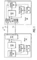
- Figure 1 shows a pair of devices 100 and 102 that incorporate the present techniques.
- the device 100 includes a local clock 10 and the device 102 includes a local clock 12.
- the devices 100 and 102 maintain time synchronization in the local clocks 10 and 12 by exchanging timing information via a communication link 110.
- the devices 100 and 102 determine an asymmetry between a propagation delay on a first portion 112 of the communication link 110 and a propagation delay on a second portion 114 of the communication link 110 and incorporate the asymmetry into a determination of a clock offset between the local clocks 10 and 12.
- the devices 100 and 102 determine a clock offset by exchanging timing packets and measuring the transmit and receive times of the timing packets according to the IEEE 1588 time synchronization protocol.
- Example embodiments of the devices 100 and 102 include computer systems, test instruments, industrial control devices, environmental control devices, home appliances, etc.
- the devices 100 includes a processor subsystem 204 and the device 102 includes a processor subsystem 224.
- the processor subsystems 204 and 224 generate timing packets and exchange the timing packets via the communication link 110.
- the local clock 10 is a master clock and the local clock 12 is a slave clock according to the IEEE 1588 time synchronization protocol.
- the device 100 includes a physical interface circuit (PHY) 200 and a media access circuit (MAC) 202 that enable the transmission and reception of timing packets via the communication link 110.
- the processor subsystem 204 in the device 100 includes code that provides a network protocol stack for communication via the communication link 110.
- the device 102 includes a PHY 220 and a MAC 222 that enable the transmission and reception of timing packets and the processor subsystem 224 includes code that provides a network protocol stack for communication via the communication link 110.
- the device 100 includes a timing packet recognizer 30 that snoops a data path 230 between the MAC 202 and the PHY 200.
- the timing packet recognizer 30 generates timestamps in response to timing packets on the data path 230.
- the device 102 includes a timing packet recognizer 32 that snoops a data path 232 between the MAC 222 and the PHY 220 and that generates timestamps in response to timing packets on the data path 232.
- the processor subsystems 204 and 224 obtain timestamp measurements from their respective timing packet recognizers 30 and 32 and exchange time stamp measurements with one another using packets carried on the communication link 110.
- the timestamp measurements enable a determination of a clock offset between the time held in the local clock 10 and the time held in the local clock 12.
- the processor 224 uses the clock offset to perform time adjustments to the local clock 12 which is a slave clock in this example.
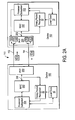
- Figures 2a-2b illustrate a technique for measuring an asymmetry of the communication link 110 by running a time synchronization experiment (experiment A) to determine a first clock offset for the local clocks 10 and 12 and then reconfiguring the directions of transmission on the first and second portions 112 and 114 and running another time synchronization experiment (experiment B) to determine a second clock offset for the local clocks 10 and 12.
- the asymmetry is derived from the first and second clock offsets.
- the measurement and computation of clock offsets using two different configurations of the communication link 110 enables the common and differential mode propagation times on the communication link 110 to be determined. The differential contribution is then used to correct the normal operation and eliminate the clock offset error that would otherwise occur.
- the processor subsystem 204 In the experiment A ( Figure 2a ), the processor subsystem 204 generates a timing packet 40-a and transfers the timing packet 40-a to the device 102 via the first portion 112 using the MAC 202 and the PHY 200.
- the timing packet recognizer 30 generates a timestamp T1-a in response to the timing packet 40-a on the data path 230.
- the processor subsystem 224 receives the timing packet 40-a using the PHY 220 and the MAC 222.
- the timing packet recognizer 32 generates a timestamp T2-a in response to the timing packet 40-a on the data path 232.
- the processor subsystem 224 generates a timing packet 42-a and transfers it to the device 100 via the second portion 114 using the MAC 222 and the PHY 220.
- the timing packet recognizer 32 generates a timestamp T3-a in response to the timing packet 42-a on the data path 232.
- the processor subsystem 204 receives the timing packet 42-a using the PHY 200 and the MAC 202 and the timing packet recognizer 30 generates a timestamp T4-a in response to the timing packet 42-a on the data path 230.
- the timestamps T1-a through T4-a yielded by the experiment A enable a determination of a first clock offset (OFFSET-a) between the local clocks 10 and 12 for a configuration of the communication link 110 in which the first portion 112 carries information from the device 100 to the device 102 and the second portion 114 carries information from the device 102 to the device 100.
- the communication link 110 is then reconfigured for the experiment B so that the second portion 114 carries information from the device 100 to the device 102 and the first portion 112 carries information from the device 102 to the device 100.
- the processor subsystem 204 In the experiment B ( Figure 2b), the processor subsystem 204 generates a timing packet 40-b and transfers the timing packet 40-b to the device 102 via the second portion 114 using the MAC 202 and the PHY 200.
- the timing packet recognizer 30 generates a timestamp T1-b in response to the timing packet 40-b on the data path 230.
- the processor subsystem 224 receives the timing packet 40-b using the PHY 220 and the MAC 222 and the timing packet recognizer 32 generates a timestamp T2-b in response to the timing packet 40-b on the data path 232.
- the processor subsystem 224 generates a timing packet 42-b and transfers it to the device 100 via the first portion 112 using the MAC 222 and the PHY 220.
- the timing packet recognizer 32 generates a timestamp T3-b in response to the timing packet 42-b on the data path 232.
- the processor subsystem 204 receives the timing packet 42-b using the PHY 202 and the MAC 200 and the timing packet recognizer 30 generates a timestamp T4-b in response to the timing packet 42-b on the data path 230.
- the timestamps T1-b through T4-b enable a determination of a second clock offset (OFFSET-b) between the local clocks 10 and 12 for a configuration of the communication link 110 in which the second portion 114 carries information from the device 100 to the device 102 and the first portion 112 carries information from the device 102 to the device 100.
- An asymmetry between the first and second portions 112 and 114 of the communication link 110 may then be derived from the OFFSET-a and OFFSET-b.
- the PHY 220 in the device 102 includes a receiver 130 and a transmitter 132 for the first portion 112 and a transmitter 140 and a receiver 142 for the second portion 114.
- the processor subsystem 224 places the communication link 110 into the configuration for the experiment A by sending a signal to the PHY 220 that causes the PHY 220 to enable the receiver 130 and the transmitter 140 and disable the transmitter 132 and the receiver 142.
- the processor subsystem 224 places the communication link 110 into the configuration for the experiment B by sending a signal to the PHY 220 that causes the PHY 220 to disable the receiver 130 and the transmitter 140 and enable the transmitter 132 and the receiver 142.
- the PHY 220 includes one receiver and one transmitter and a switching circuit that connects the transmitter to the first portion 112 and the receiver to the second portion 114, or visa versa, under command of the processor subsystem 224.
- the PHY 200 includes circuitry for sensing which of the first and second portions 112 and 114 is the transmit line and which is the receive line to the device 100.
- the capability of sensing transmit and receive lines may be implemented in the device 100 in accordance with Ethernet standards.
- Ethernet includes the auto-MDIX protocol for sensing transmit and receive lines and for and switching the transmit and receive lines to the PHY 200.
- the PHY 200 may sense any traffic, special auto-MDIX signals, etc.
- the PHY 200 senses the timing packet 42-a from the device 102 on the second portion 114, it indicates that the second portion 114 is the receive line to the device 100. If the PHY 200 senses the timing packet 42-b from the device 102 on the first portion 112, it indicates that the first portion 112 is the receive line to the device 100.
- the capability of sensing transmit and receive lines may be implemented in the device 100 in accordance with Ethernet standards.
- predetermined signaling on the communication link 110 is used to switch transmit and receive lines for the explicit purpose of measuring asymmetry.
- the device 102 may send a command to the device 100 to cause it to reverse the transmit and receive lines at the device 100 to correspond to an analogous reversal at the device 102.
- the processor subsystem 224 may send a command packet to the processor subsystem 204 that causes the processor subsystem 204 to reverse the transmit and receive lines of the PHY 200 using, for example, a switching circuit, relay, etc. in the device 100, while the processor subsystem 224 reverses the transmit and receive lines of the PHY 220.
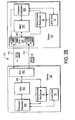
- Figure 3 shows a relay 120 placed between the PHY 220 and a connector 122 that couples the device 102 to the communication link 110.
- the relay 120 is controlled by a signal from the processor subsystem 224.
- the processor subsystem 224 controls which of the first and second portions 112 and 114 is the transmit line and which is the receive line to the device 102 by controlling the settings of the relay 120.
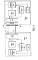
- Figures 4a-4b illustrate a determination of the asymmetry of the communication link 110 from the experiments A and B using IEEE 1588 time synchronization calculations.
- the propagation delays on the communication link 110 are expressed in terms of a mean delay, the common mode part, and a differential delay as follows.
- ⁇ ⁇ ⁇ m + ⁇ a
- ⁇ ⁇ ⁇ m - ⁇ a
- Figure 4a represents the configuration for the experiment A in which the device 100 is the master that sends timing packets on wire alpha and the device 102 is the slave that sends the timing packets on wire beta.
- the master sends sync packets and the slave sends Delay_Req packets. From the timing diagram, the following equations can be derived by inspection.
- Figure 4b represents the configuration for the experiment B in which the master sends the Sync packets on wire beta and the slave sends the Delay_Req packet on wire alpha.
- the propagation delay values do not reverse. From the timing diagram the following equations can be derived by inspection.
- ⁇ B - ⁇ A + 2 ⁇ ⁇ a + 1 2 T 2 ⁇ B - T 1 ⁇ B - ( T 2 ⁇ A - T 1 ⁇ A ) - ( T 4 ⁇ B - T 3 ⁇ B ) + ( T 4 ⁇ A - T 3 ⁇ A )
- the condition that the clock offsets do not change between the experiments A and B may be realized by operating the slave clock in both experiments A and B such that the only clock adjustments are those that keep the rates equal. This ensures that all measurements use the same definition of a second. A sufficient number of data points are then taken in each experiment A and B to reduce the effects of measurement noise and allowing more accurate computation of the asymmetry. Once this is done, the asymmetry is used to correct the measurements made during the normal operation of the synchronization protocol.
- FIG. 5 shows an embodiment of the device 102 includes a time domain reflectometry (TDR) circuit 74 for measuring an asymmetry of the communication link 110.
- the TDR circuit 74 measures an asymmetry between a propagation delay on the first portion 112 of the communication link 110 and a propagation delay on the second portion 114 of the communication link 110.
- the TDR circuit 74 includes a pulse generator circuit 80 that transmits a pulse on the first portion 112 and a pulse on the second portion 114 at substantially the same time.
- the pulses on the first portion 112 and second portion 114 propagate to the device 100 and are reflected back to the TDR circuit 74 via the first portion 112 and the second portion 114.
- the TDR circuit 74 includes a pulse detector circuit 82 that detects the arrival of the reflected pulses on the first portion 112 and second portion 114.
- the TDR circuit 74 includes a timing circuit 84 that measures the times between generation of the pulses by the pulse generator 80 and the arrival of the corresponding pulse reflections via the first portion 112 and second portion 114.
- the timing circuit 84 may include a pair of respective counters for the first portion 112 and the second portion 114 such that the respective counters are started when the corresponding pulse is generated by the pulse generator 80 and are stopped upon receipt of the corresponding reflected pulse via the first portion 112 and the second portion 114.
- the difference in the counts indicates an asymmetry between the propagation delays on the first and second portions 112 and 114.
- the TDR circuit 74 may include switching circuitry for applying pulses to the first portion 112 and the second portion 114 and for sensing reflected pulses on the first portion 112 and the second portion 114.
- the switching circuitry may be used to prevent interaction with the PHY 220 in the device 102.
- the TDR circuit 74 may employ transformers for applying pulses to and sensing pulses on the first portion 112 and the second portion 114.
- the measurement functions of the TDR circuit 74 may be activated by a command from the processor subsystem 224 sent via a command/data path 88.
- the processor subsystem 224 may obtain asymmetry measurements from the TDR circuit 74 via the command/data path 88.
- the energy in a pulse generated by the TDR circuit 74 may be selected to prevent damage to circuitry in the device 100, e.g. based on the physical implementations of the communication link 100 and the devices 100 and 102.
- the device 100 may include a protection circuit (not shown) at the connection to the communication link 110. If the TDR 74 uses pulses with low energy then no protection is needed at device 100. If the TDR 74 uses pulses with higher energy then protection might be needed. Sufficient protection may be provided for other reasons such as electrostatic effects, etc.
- the pulse energy may be selected to be high enough to activate protection circuitry. If the protection circuit is fast, e.g.
- the protection circuit may present an impedance mismatch to the communication link 110 so that more energy may be provided in reflected pulses that are returned to the TDR circuit 74.
- the TDR circuit 74 may apply the pulses on the first portion 112 and the second portion 114 substantially simultaneously and at the same electrical distance from the attachment point on the first portion 112 and the second portion 114.
- the TDR circuit 74 may use the local clock 12 as a time reference so that the measured asymmetry has the same time base as the time adjustment computations.
- the asymmetry may be measured to a resolution below that of the local clock 12 by employing delay lines and multiple time stamping, interpolating counters, or interpolating ramps.
Landscapes
- Engineering & Computer Science (AREA)
- Computer Networks & Wireless Communication (AREA)
- Signal Processing (AREA)
- Synchronisation In Digital Transmission Systems (AREA)
- Small-Scale Networks (AREA)
- Data Exchanges In Wide-Area Networks (AREA)
Abstract
Description
- A wide variety of devices may include a local clock that maintains a time-of-day. Examples of devices that may have a local time-of-day clock include computer systems, test instruments, industrial control devices, environmental control devices, and home appliances.
- A time synchronization protocol may be used to synchronize a local clock in a device. A time synchronization protocol may be one in which a device exchanges timing information with a reference time source via a communication link. The exchanged timing information may be used to determine a clock offset that indicates a relative time difference between a local clock and a reference time source. For example, the IEEE 1588 time synchronization protocol includes the exchange of timing packets via a communication link.
- Asymmetric delays on a communication link may reduce the accuracy of time synchronization. In IEEE 1588 time synchronization, for example, a propagation delay experienced by a timing packet in one direction over an Ethernet cable may differ from a propagation delay experienced by a timing packet in the opposite direction over the Ethernet cable. Similar asymmetric delays may occur on fiber optic cables and wireless communication links. Unfortunately, a time synchronization protocol may base its clock offset calculations on an assumption that the delays on a communication link are symmetric and any asymmetry in the delays may reduce the accuracy of time synchronization.
- Techniques are disclosed for correcting time synchronization inaccuracy caused by asymmetric delays on a communication link. Time synchronization according to the present techniques includes determining an asymmetry in a propagation delay on a communication link used by a first device and a second device to exchange timing information and incorporating the asymmetry into a determination of a clock offset between the first and second devices.
- Other features and advantages of the present invention will be apparent from the detailed description that follows.
- The present invention is described with respect to particular exemplary embodiments thereof and reference is accordingly made to the drawings in which:
- Figure 1 shows a pair of devices and that implement the present techniques;
- Figures 2a-2b illustrate a technique for measuring an asymmetry of a communication link;
- Figure 3 shows a relay for reversing the transmit and receive lines of a communication link;
- Figures 4a-4b illustrate a determination of an asymmetry of a communication link using IEEE 1588 time synchronization calculations;
- Figure 5 shows a device that includes a time domain reflectometry (TDR) circuit for measuring an asymmetry of a communication link.
- Figure 1 shows a pair of
devices device 100 includes alocal clock 10 and thedevice 102 includes alocal clock 12. Thedevices local clocks communication link 110. Thedevices first portion 112 of thecommunication link 110 and a propagation delay on asecond portion 114 of thecommunication link 110 and incorporate the asymmetry into a determination of a clock offset between thelocal clocks devices - Example embodiments of the
devices - The
devices 100 includes aprocessor subsystem 204 and thedevice 102 includes aprocessor subsystem 224. The processor subsystems 204 and 224 generate timing packets and exchange the timing packets via thecommunication link 110. In the example shown, thelocal clock 10 is a master clock and thelocal clock 12 is a slave clock according to the IEEE 1588 time synchronization protocol. - The
device 100 includes a physical interface circuit (PHY) 200 and a media access circuit (MAC) 202 that enable the transmission and reception of timing packets via thecommunication link 110. Theprocessor subsystem 204 in thedevice 100 includes code that provides a network protocol stack for communication via thecommunication link 110. Similarly, thedevice 102 includes aPHY 220 and aMAC 222 that enable the transmission and reception of timing packets and theprocessor subsystem 224 includes code that provides a network protocol stack for communication via thecommunication link 110. - The
device 100 includes a timing packet recognizer 30 that snoops adata path 230 between theMAC 202 and the PHY 200. The timing packet recognizer 30 generates timestamps in response to timing packets on thedata path 230. Thedevice 102 includes a timing packet recognizer 32 that snoops adata path 232 between theMAC 222 and thePHY 220 and that generates timestamps in response to timing packets on thedata path 232. - The processor subsystems 204 and 224 obtain timestamp measurements from their respective
timing packet recognizers communication link 110. The timestamp measurements enable a determination of a clock offset between the time held in thelocal clock 10 and the time held in thelocal clock 12. Theprocessor 224 uses the clock offset to perform time adjustments to thelocal clock 12 which is a slave clock in this example. - Figures 2a-2b illustrate a technique for measuring an asymmetry of the
communication link 110 by running a time synchronization experiment (experiment A) to determine a first clock offset for thelocal clocks second portions local clocks communication link 110 enables the common and differential mode propagation times on thecommunication link 110 to be determined. The differential contribution is then used to correct the normal operation and eliminate the clock offset error that would otherwise occur. - In the experiment A (Figure 2a), the
processor subsystem 204 generates a timing packet 40-a and transfers the timing packet 40-a to thedevice 102 via thefirst portion 112 using theMAC 202 and the PHY 200. Thetiming packet recognizer 30 generates a timestamp T1-a in response to the timing packet 40-a on thedata path 230. Theprocessor subsystem 224 receives the timing packet 40-a using the PHY 220 and the MAC 222. Thetiming packet recognizer 32 generates a timestamp T2-a in response to the timing packet 40-a on thedata path 232. - Thereafter, the
processor subsystem 224 generates a timing packet 42-a and transfers it to thedevice 100 via thesecond portion 114 using the MAC 222 and the PHY 220. Thetiming packet recognizer 32 generates a timestamp T3-a in response to the timing packet 42-a on thedata path 232. Theprocessor subsystem 204 receives the timing packet 42-a using the PHY 200 and theMAC 202 and thetiming packet recognizer 30 generates a timestamp T4-a in response to the timing packet 42-a on thedata path 230. - The timestamps T1-a through T4-a yielded by the experiment A enable a determination of a first clock offset (OFFSET-a) between the
local clocks communication link 110 in which thefirst portion 112 carries information from thedevice 100 to thedevice 102 and thesecond portion 114 carries information from thedevice 102 to thedevice 100. Thecommunication link 110 is then reconfigured for the experiment B so that thesecond portion 114 carries information from thedevice 100 to thedevice 102 and thefirst portion 112 carries information from thedevice 102 to thedevice 100. - In the experiment B (Figure 2b), the
processor subsystem 204 generates a timing packet 40-b and transfers the timing packet 40-b to thedevice 102 via thesecond portion 114 using theMAC 202 and thePHY 200. Thetiming packet recognizer 30 generates a timestamp T1-b in response to the timing packet 40-b on thedata path 230. Theprocessor subsystem 224 receives the timing packet 40-b using the PHY 220 and theMAC 222 and thetiming packet recognizer 32 generates a timestamp T2-b in response to the timing packet 40-b on thedata path 232. Theprocessor subsystem 224 generates a timing packet 42-b and transfers it to thedevice 100 via thefirst portion 112 using theMAC 222 and the PHY 220. Thetiming packet recognizer 32 generates a timestamp T3-b in response to the timing packet 42-b on thedata path 232. Theprocessor subsystem 204 receives the timing packet 42-b using the PHY 202 and the MAC 200 and thetiming packet recognizer 30 generates a timestamp T4-b in response to the timing packet 42-b on thedata path 230. - The timestamps T1-b through T4-b enable a determination of a second clock offset (OFFSET-b) between the
local clocks communication link 110 in which thesecond portion 114 carries information from thedevice 100 to thedevice 102 and thefirst portion 112 carries information from thedevice 102 to thedevice 100. An asymmetry between the first andsecond portions communication link 110 may then be derived from the OFFSET-a and OFFSET-b. - In one embodiment, the
PHY 220 in thedevice 102 includes areceiver 130 and atransmitter 132 for thefirst portion 112 and atransmitter 140 and areceiver 142 for thesecond portion 114. In this embodiment, theprocessor subsystem 224 places thecommunication link 110 into the configuration for the experiment A by sending a signal to thePHY 220 that causes thePHY 220 to enable thereceiver 130 and thetransmitter 140 and disable thetransmitter 132 and thereceiver 142. Theprocessor subsystem 224 places thecommunication link 110 into the configuration for the experiment B by sending a signal to thePHY 220 that causes thePHY 220 to disable thereceiver 130 and thetransmitter 140 and enable thetransmitter 132 and thereceiver 142. In another embodiment, thePHY 220 includes one receiver and one transmitter and a switching circuit that connects the transmitter to thefirst portion 112 and the receiver to thesecond portion 114, or visa versa, under command of theprocessor subsystem 224. - The
PHY 200 includes circuitry for sensing which of the first andsecond portions device 100. The capability of sensing transmit and receive lines may be implemented in thedevice 100 in accordance with Ethernet standards. For example, Ethernet includes the auto-MDIX protocol for sensing transmit and receive lines and for and switching the transmit and receive lines to thePHY 200. ThePHY 200 may sense any traffic, special auto-MDIX signals, etc. - In another example, if the
PHY 200 senses the timing packet 42-a from thedevice 102 on thesecond portion 114, it indicates that thesecond portion 114 is the receive line to thedevice 100. If thePHY 200 senses the timing packet 42-b from thedevice 102 on thefirst portion 112, it indicates that thefirst portion 112 is the receive line to thedevice 100. The capability of sensing transmit and receive lines may be implemented in thedevice 100 in accordance with Ethernet standards. - In other embodiments, predetermined signaling on the
communication link 110 is used to switch transmit and receive lines for the explicit purpose of measuring asymmetry. Thedevice 102 may send a command to thedevice 100 to cause it to reverse the transmit and receive lines at thedevice 100 to correspond to an analogous reversal at thedevice 102. For example, theprocessor subsystem 224 may send a command packet to theprocessor subsystem 204 that causes theprocessor subsystem 204 to reverse the transmit and receive lines of thePHY 200 using, for example, a switching circuit, relay, etc. in thedevice 100, while theprocessor subsystem 224 reverses the transmit and receive lines of thePHY 220. - Figure 3 shows a relay 120 placed between the
PHY 220 and aconnector 122 that couples thedevice 102 to thecommunication link 110. The relay 120 is controlled by a signal from theprocessor subsystem 224. Theprocessor subsystem 224 controls which of the first andsecond portions device 102 by controlling the settings of the relay 120. - Figures 4a-4b illustrate a determination of the asymmetry of the
communication link 110 from the experiments A and B using IEEE 1588 time synchronization calculations. In the following, the propagation delays on thecommunication link 110 are expressed in terms of a mean delay, the common mode part, and a differential delay as follows.

- These are properties of the wires in the
first portion 112 and thesecond portion 114 of thecommunication link 110. - Figure 4a represents the configuration for the experiment A in which the
device 100 is the master that sends timing packets on wire alpha and thedevice 102 is the slave that sends the timing packets on wire beta. In the IEEE 1588 protocol, the master sends sync packets and the slave sends Delay_Req packets. From the timing diagram, the following equations can be derived by inspection.

- From these equations the values of the mean propagation time and the offset can be determined as follows.


- Figure 4b represents the configuration for the experiment B in which the master sends the Sync packets on wire beta and the slave sends the Delay_Req packet on wire alpha. The propagation delay values do not reverse. From the timing diagram the following equations can be derived by inspection.


- From these equations the values of the mean propagation time and the offset can be determined as follows.


- Comparing the equations for the experiment B with the corresponding equations for the experiment A, it is clear that the mean delay computation has the same form, i.e. the common mode. However the computation of the clock offset differs in the sign of the asymmetry term.
- Thus, the difference of the clock offsets for the experiments A and B is as follows.

- If the clock offsets do not change between experiments A and B then the following can be observed.


- The condition that the clock offsets do not change between the experiments A and B may be realized by operating the slave clock in both experiments A and B such that the only clock adjustments are those that keep the rates equal. This ensures that all measurements use the same definition of a second. A sufficient number of data points are then taken in each experiment A and B to reduce the effects of measurement noise and allowing more accurate computation of the asymmetry. Once this is done, the asymmetry is used to correct the measurements made during the normal operation of the synchronization protocol.
- Figure 5 shows an embodiment of the
device 102 includes a time domain reflectometry (TDR)circuit 74 for measuring an asymmetry of thecommunication link 110. TheTDR circuit 74 measures an asymmetry between a propagation delay on thefirst portion 112 of thecommunication link 110 and a propagation delay on thesecond portion 114 of thecommunication link 110. - The
TDR circuit 74 includes a pulse generator circuit 80 that transmits a pulse on thefirst portion 112 and a pulse on thesecond portion 114 at substantially the same time. The pulses on thefirst portion 112 andsecond portion 114 propagate to thedevice 100 and are reflected back to theTDR circuit 74 via thefirst portion 112 and thesecond portion 114. - The
TDR circuit 74 includes a pulse detector circuit 82 that detects the arrival of the reflected pulses on thefirst portion 112 andsecond portion 114. TheTDR circuit 74 includes a timing circuit 84 that measures the times between generation of the pulses by the pulse generator 80 and the arrival of the corresponding pulse reflections via thefirst portion 112 andsecond portion 114. For example, the timing circuit 84 may include a pair of respective counters for thefirst portion 112 and thesecond portion 114 such that the respective counters are started when the corresponding pulse is generated by the pulse generator 80 and are stopped upon receipt of the corresponding reflected pulse via thefirst portion 112 and thesecond portion 114. The difference in the counts indicates an asymmetry between the propagation delays on the first andsecond portions - The
TDR circuit 74 may include switching circuitry for applying pulses to thefirst portion 112 and thesecond portion 114 and for sensing reflected pulses on thefirst portion 112 and thesecond portion 114. The switching circuitry may be used to prevent interaction with thePHY 220 in thedevice 102. Alternatively, theTDR circuit 74 may employ transformers for applying pulses to and sensing pulses on thefirst portion 112 and thesecond portion 114. The measurement functions of theTDR circuit 74 may be activated by a command from theprocessor subsystem 224 sent via a command/data path 88. Theprocessor subsystem 224 may obtain asymmetry measurements from theTDR circuit 74 via the command/data path 88. - The energy in a pulse generated by the
TDR circuit 74 may be selected to prevent damage to circuitry in thedevice 100, e.g. based on the physical implementations of thecommunication link 100 and thedevices device 100 may include a protection circuit (not shown) at the connection to thecommunication link 110. If theTDR 74 uses pulses with low energy then no protection is needed atdevice 100. If theTDR 74 uses pulses with higher energy then protection might be needed. Sufficient protection may be provided for other reasons such as electrostatic effects, etc. The pulse energy may be selected to be high enough to activate protection circuitry. If the protection circuit is fast, e.g. if it activates in fractions of a nanosecond, then a large impedance mismatch occurs when the protection circuit turns on, thereby increasing the return reflection. The protection circuit may present an impedance mismatch to thecommunication link 110 so that more energy may be provided in reflected pulses that are returned to theTDR circuit 74. - The
TDR circuit 74 may apply the pulses on thefirst portion 112 and thesecond portion 114 substantially simultaneously and at the same electrical distance from the attachment point on thefirst portion 112 and thesecond portion 114. - The
TDR circuit 74 may use thelocal clock 12 as a time reference so that the measured asymmetry has the same time base as the time adjustment computations. The asymmetry may be measured to a resolution below that of thelocal clock 12 by employing delay lines and multiple time stamping, interpolating counters, or interpolating ramps. - The foregoing detailed description of the present invention is provided for the purposes of illustration and is not intended to be exhaustive or to limit the invention to the precise embodiment disclosed. Accordingly, the scope of the present invention is defined by the appended claims.
Claims (10)
- A method for time synchronization, comprising:determining an asymmetry in a propagation delay on a communication link (110) used by a first device (100) and a second device (102) to exchange timing information;incorporating the asymmetry into a determination of a clock offset between the first and second devices (100, 102).
- The method of claim 1, wherein determining an asymmetry includes measuring a propagation delay on a first portion (112) of the communication link (110) and measuring a propagation delay on a second portion (114) of the communication link (110).
- The method of claim 1, wherein determining an asymmetry comprises:exchanging a first set of timing packets via the communication link (110) and determining a first clock offset in response to the first set of timing packets;reversing a direction of transmission on each of a first and second portion (112, 114) of the communication link (110);exchanging a second set of timing packets via the communication link (110) and determining a second clock offset in response to the second set of timing packets;determining the asymmetry in response to the first and second clock offsets.
- The method of claim 3, wherein reversing a direction comprises reversing a transmit line and a receive line in the second device (102).
- The method of claim 4, wherein reversing a direction further comprises reversing a transmit line and a receive line in the first device (100).
- The method of claim 5, wherein reversing a transmit line and a receive line in the first device (100) comprises sensing the transmit line and the receive line in the first device (100).
- The method of claim 5, wherein reversing a transmit line and a receive line in the first device (100) comprises sending a command to the first device (100) via the communication link (110).
- The method of claim 3, wherein the first device (100) includes a master clock and the second device (102) includes a slave clock.
- The method of claim 8, wherein incorporating the asymmetry comprises:measuring a transmit time and a receive time of each a set of sync packets transferred from the first device (100) to the second device (102) via the communication link (110) and each of a set of delay request packets transferred from the second device (102) to the first device (100) via the communication link (110) ;determining the clock offset in response to the transmit and receive times and the asymmetry.
- The method of claim 9, wherein determining the clock offset comprises determining the clock offset according to the IEEE 1588 time synchronization protocol.
Applications Claiming Priority (1)
| Application Number | Priority Date | Filing Date | Title |
|---|---|---|---|
| US11/317,294 US7602873B2 (en) | 2005-12-23 | 2005-12-23 | Correcting time synchronization inaccuracy caused by asymmetric delay on a communication link |
Publications (1)
| Publication Number | Publication Date |
|---|---|
| EP1802014A1 true EP1802014A1 (en) | 2007-06-27 |
Family
ID=37605721
Family Applications (1)
| Application Number | Title | Priority Date | Filing Date |
|---|---|---|---|
| EP06255837A Withdrawn EP1802014A1 (en) | 2005-12-23 | 2006-11-15 | Correcting time synchronisation inaccuracy caused by asymmetric delay on a communication link |
Country Status (4)
| Country | Link |
|---|---|
| US (1) | US7602873B2 (en) |
| EP (1) | EP1802014A1 (en) |
| JP (1) | JP4922750B2 (en) |
| CN (1) | CN101098219A (en) |
Cited By (13)
| Publication number | Priority date | Publication date | Assignee | Title |
|---|---|---|---|---|
| EP2234442A2 (en) * | 2009-03-24 | 2010-09-29 | Fujitsu Limited | Radio base station apparatus and synchronization method thereof |
| WO2011079460A1 (en) | 2009-12-31 | 2011-07-07 | Abb Research Ltd. | Method and apparatus for detecting communication channel delay asymmetry |
| WO2011144263A1 (en) * | 2010-05-17 | 2011-11-24 | Telefonaktiebolaget L M Ericsson (Publ) | Optimizing timing packet transport |
| EP2568756A1 (en) * | 2011-09-09 | 2013-03-13 | Huawei Technologies Co., Ltd. | Time synchronization method and system, and node device |
| EP2619936A1 (en) * | 2010-09-20 | 2013-07-31 | Alcatel Lucent | Method for correcting an asymmetry in a delay |
| EP2731303A1 (en) * | 2011-08-10 | 2014-05-14 | ZTE Corporation | Method and device for implementing automatic compensation for asymmetric delay of 1588 link |
| WO2014137630A3 (en) * | 2013-03-05 | 2014-11-06 | Qualcomm Incorporated | Reducing impact of clock drift in wireless devices |
| WO2015169363A1 (en) * | 2014-05-08 | 2015-11-12 | Telefonaktiebolaget L M Ericsson (Publ) | Method and apparatus for determining propagation delay in a communications network |
| EP2924889A4 (en) * | 2012-11-20 | 2015-12-16 | Zte Corp | Synchronization system, method and master/slave optical module device for detecting asymmetry of optical fiber |
| EP2706686B1 (en) * | 2011-05-03 | 2019-06-12 | ZTE Corporation | Method, terminal and system for measuring asymmetric delay of transmission link |
| WO2022122333A1 (en) * | 2020-12-11 | 2022-06-16 | Nokia Technologies Oy | Asymmetric propagation delay detection and response for wireless networks |
| WO2023052396A1 (en) * | 2021-10-01 | 2023-04-06 | Net Insight Ab | Assymetric delay compensation |
| WO2024047177A1 (en) * | 2022-09-01 | 2024-03-07 | OTN Systems N.V. | A method for delay monitoring |
Families Citing this family (76)
| Publication number | Priority date | Publication date | Assignee | Title |
|---|---|---|---|---|
| DE102006031580A1 (en) | 2006-07-03 | 2008-01-17 | Faro Technologies, Inc., Lake Mary | Method and device for the three-dimensional detection of a spatial area |
| US8036202B2 (en) * | 2006-07-27 | 2011-10-11 | Cisco Technology, Inc. | Physical layer transceiver with integrated time synchronization |
| US8325767B2 (en) * | 2006-09-29 | 2012-12-04 | Agilent Technologies, Inc. | Enhancement of IEEE 1588 synchronization using out-of-band communication path |
| US20080103713A1 (en) * | 2006-10-27 | 2008-05-01 | Barford Lee A | Labeling Asymmetric Cables For Improved Network Clock Synchronization |
| CN101196966B (en) * | 2006-12-08 | 2010-05-19 | 华为技术有限公司 | Method for license interaction and recovery after break-up, and digital copyright management system |
| US8233432B2 (en) * | 2007-08-31 | 2012-07-31 | Silicon Image, Inc. | Ensuring physical locality of entities sharing data |
| EP2034642B1 (en) * | 2007-09-07 | 2011-10-26 | Siemens Aktiengesellschaft | Method for transmitting synchronisation messages in a communications network |
| DE102008036221A1 (en) * | 2008-08-02 | 2010-02-04 | Bayerische Motoren Werke Aktiengesellschaft | Timer adjusting method for master node of bus system of ring network in motor vehicle, involves sending first and second delays to receiver, where third delay is calculated as difference between first and second delays |
| JP5228714B2 (en) * | 2008-09-02 | 2013-07-03 | 富士通株式会社 | Time synchronization method and relay device |
| US20100150288A1 (en) * | 2008-12-17 | 2010-06-17 | Miao Zhu | Synchronization of Low Noise Local Oscillator using Network Connection |
| CN101783779B (en) * | 2009-01-16 | 2014-07-16 | 华为技术有限公司 | Time synchronization method, device and system of xDSL |
| US9551575B2 (en) | 2009-03-25 | 2017-01-24 | Faro Technologies, Inc. | Laser scanner having a multi-color light source and real-time color receiver |
| DE102009015920B4 (en) | 2009-03-25 | 2014-11-20 | Faro Technologies, Inc. | Device for optically scanning and measuring an environment |
| CN102035613A (en) * | 2009-09-28 | 2011-04-27 | 华为技术有限公司 | Method, device and network system for realizing time synchronization |
| US9113023B2 (en) | 2009-11-20 | 2015-08-18 | Faro Technologies, Inc. | Three-dimensional scanner with spectroscopic energy detector |
| DE102009057101A1 (en) | 2009-11-20 | 2011-05-26 | Faro Technologies, Inc., Lake Mary | Device for optically scanning and measuring an environment |
| US9210288B2 (en) | 2009-11-20 | 2015-12-08 | Faro Technologies, Inc. | Three-dimensional scanner with dichroic beam splitters to capture a variety of signals |
| US9529083B2 (en) | 2009-11-20 | 2016-12-27 | Faro Technologies, Inc. | Three-dimensional scanner with enhanced spectroscopic energy detector |
| CN102082697A (en) | 2009-11-27 | 2011-06-01 | 华为技术有限公司 | Communication path asymmetric time delay measuring method, device and system |
| WO2011074664A1 (en) * | 2009-12-18 | 2011-06-23 | 株式会社エヌ・ティ・ティ・ドコモ | Wireless base station, and relay device |
| CN104052564B (en) * | 2009-12-31 | 2017-01-18 | Abb研究有限公司 | Method and device for detecting channel delay asymmetry |
| US8630314B2 (en) | 2010-01-11 | 2014-01-14 | Faro Technologies, Inc. | Method and apparatus for synchronizing measurements taken by multiple metrology devices |
| US9879976B2 (en) | 2010-01-20 | 2018-01-30 | Faro Technologies, Inc. | Articulated arm coordinate measurement machine that uses a 2D camera to determine 3D coordinates of smoothly continuous edge features |
| US9163922B2 (en) | 2010-01-20 | 2015-10-20 | Faro Technologies, Inc. | Coordinate measurement machine with distance meter and camera to determine dimensions within camera images |
| US8832954B2 (en) | 2010-01-20 | 2014-09-16 | Faro Technologies, Inc. | Coordinate measurement machines with removable accessories |
| US8898919B2 (en) | 2010-01-20 | 2014-12-02 | Faro Technologies, Inc. | Coordinate measurement machine with distance meter used to establish frame of reference |
| US9628775B2 (en) | 2010-01-20 | 2017-04-18 | Faro Technologies, Inc. | Articulated arm coordinate measurement machine having a 2D camera and method of obtaining 3D representations |
| US8284407B2 (en) | 2010-01-20 | 2012-10-09 | Faro Technologies, Inc. | Coordinate measuring machine having an illuminated probe end and method of operation |
| CN102712091A (en) | 2010-01-20 | 2012-10-03 | 法罗技术股份有限公司 | Embedded arm strain sensors |
| US8638446B2 (en) | 2010-01-20 | 2014-01-28 | Faro Technologies, Inc. | Laser scanner or laser tracker having a projector |
| US8677643B2 (en) | 2010-01-20 | 2014-03-25 | Faro Technologies, Inc. | Coordinate measurement machines with removable accessories |
| US9607239B2 (en) | 2010-01-20 | 2017-03-28 | Faro Technologies, Inc. | Articulated arm coordinate measurement machine having a 2D camera and method of obtaining 3D representations |
| US8875409B2 (en) | 2010-01-20 | 2014-11-04 | Faro Technologies, Inc. | Coordinate measurement machines with removable accessories |
| CN102713776B (en) | 2010-01-20 | 2015-04-22 | 法罗技术股份有限公司 | Portable articulated arm coordinate measuring machine with multi-bus arm technology |
| US8615893B2 (en) | 2010-01-20 | 2013-12-31 | Faro Technologies, Inc. | Portable articulated arm coordinate measuring machine having integrated software controls |
| CN102158945B (en) * | 2010-02-12 | 2014-04-02 | 华为技术有限公司 | Method for time synchronization in digital subscriber line communication system, device and system |
| CN101814984B (en) * | 2010-04-09 | 2012-06-27 | 华为技术有限公司 | Method and device for acquiring asymmetric delay time |
| DE102010020925B4 (en) | 2010-05-10 | 2014-02-27 | Faro Technologies, Inc. | Method for optically scanning and measuring an environment |
| US9168654B2 (en) | 2010-11-16 | 2015-10-27 | Faro Technologies, Inc. | Coordinate measuring machines with dual layer arm |
| JP2012191361A (en) * | 2011-03-09 | 2012-10-04 | Mitsubishi Electric Corp | Synchronous control system |
| CN102291178B (en) * | 2011-09-08 | 2014-11-19 | 烽火通信科技股份有限公司 | Method and device for measuring the asymmetrical time delay of optical fiber |
| JP2013083451A (en) * | 2011-10-06 | 2013-05-09 | Sony Corp | Time control device, time control method, and program |
| JP2013092515A (en) * | 2011-10-06 | 2013-05-16 | Sony Corp | Frequency difference detection device, frequency difference detection method, and program |
| CN103139002B (en) * | 2011-11-30 | 2017-12-29 | 中兴通讯股份有限公司 | 1588 thing error detection method and devices between network element |
| JP6214008B2 (en) * | 2012-01-04 | 2017-10-18 | マーベル ワールド トレード リミテッド | Method and apparatus for communicating time information between time recognition devices |
| CN102546009B (en) * | 2012-01-17 | 2014-12-24 | 华为技术有限公司 | Optical fiber symmetry detecting method and device |
| DE102012100609A1 (en) | 2012-01-25 | 2013-07-25 | Faro Technologies, Inc. | Device for optically scanning and measuring an environment |
| EP2597791B1 (en) * | 2012-02-21 | 2018-08-15 | Huawei Technologies Co., Ltd. | Method and device for compensating for time path |
| CN102594542A (en) * | 2012-03-22 | 2012-07-18 | 杭州华三通信技术有限公司 | Method and device for realizing precise time synchronization |
| JP5915379B2 (en) | 2012-05-25 | 2016-05-11 | 富士通株式会社 | Transmission apparatus and transmission method |
| EP2863576A4 (en) | 2012-06-19 | 2015-12-30 | Nec Corp | Clock synchronization system, clock synchronization method, and storage medium whereupon clock synchronization program is stored |
| US8997362B2 (en) | 2012-07-17 | 2015-04-07 | Faro Technologies, Inc. | Portable articulated arm coordinate measuring machine with optical communications bus |
| US9513107B2 (en) | 2012-10-05 | 2016-12-06 | Faro Technologies, Inc. | Registration calculation between three-dimensional (3D) scans based on two-dimensional (2D) scan data from a 3D scanner |
| US10067231B2 (en) | 2012-10-05 | 2018-09-04 | Faro Technologies, Inc. | Registration calculation of three-dimensional scanner data performed between scans based on measurements by two-dimensional scanner |
| DE102012109481A1 (en) | 2012-10-05 | 2014-04-10 | Faro Technologies, Inc. | Device for optically scanning and measuring an environment |
| US9264132B2 (en) * | 2013-01-07 | 2016-02-16 | Microsemi Frequency And Time Corporation | Universal asymmetry compensation for packet timing protocols |
| JP2014238357A (en) * | 2013-06-10 | 2014-12-18 | ソニー株式会社 | Reception device, time difference calculation method and program |
| US20150078405A1 (en) * | 2013-09-18 | 2015-03-19 | Alcatel Lucent Canada Inc. | Monitoring clock accuracy in asynchronous traffic environments |
| CN104993900B (en) * | 2015-07-06 | 2018-03-09 | 江苏省电力公司南京供电公司 | A kind of synchronization correction method based on IEEE1588 clock models |
| JP6456787B2 (en) * | 2015-07-14 | 2019-01-23 | 日本電信電話株式会社 | Time synchronization apparatus and time synchronization method |
| JP2017022647A (en) * | 2015-07-14 | 2017-01-26 | 日本電信電話株式会社 | Time synchronization apparatus and time synchronization method |
| DE102015122844A1 (en) | 2015-12-27 | 2017-06-29 | Faro Technologies, Inc. | 3D measuring device with battery pack |
| US9872189B2 (en) * | 2016-03-31 | 2018-01-16 | Corning Optical Communications Wireless Ltd | Systems and methods for determining asymmetric downlink and uplink propagation delays in a wireless distribution system (WDS) for more accurately determining propagation delay |
| US10298346B2 (en) * | 2016-06-02 | 2019-05-21 | Cisco Technology, Inc. | Directed acyclic graph optimization based on timing information for generating optimized network clock |
| US10341083B2 (en) | 2016-09-09 | 2019-07-02 | Huawei Technologies Co., Ltd. | System and methods for network synchronization |
| CN108347763B (en) * | 2017-01-24 | 2021-06-01 | 华为技术有限公司 | Time service method, terminal equipment and network equipment |
| US10142094B2 (en) * | 2017-01-24 | 2018-11-27 | Futurewei Technologies, Inc. | Synchronization error reduction in common public radio interface (CPRI) passive optical networks (PONs) |
| SG11202000761VA (en) * | 2017-07-26 | 2020-02-27 | Aviat Networks Inc | Airframe timestamping technique for point-to-point radio links |
| CN109600186B (en) * | 2018-11-20 | 2020-06-16 | Ut斯达康通讯有限公司 | Clock synchronization method and device |
| CN109980611B (en) * | 2018-11-28 | 2021-10-22 | 南京国电南自电网自动化有限公司 | Pilot differential protection adaptive synchronization method and device meeting IEEE C37.94 standard |
| US11115142B1 (en) | 2018-12-21 | 2021-09-07 | Equinix, Inc. | Timing synchronization service and distribution system |
| US11197075B1 (en) | 2018-12-27 | 2021-12-07 | Equinix, Inc. | Clock synchronization in a heterogeneous system |
| US11206095B1 (en) | 2019-03-22 | 2021-12-21 | Equinix, Inc. | Timing synchronization for clock systems with asymmetric path delay |
| US11520372B1 (en) | 2020-02-12 | 2022-12-06 | Equinix, Inc. | Time synchronization using skew estimation |
| US11431425B2 (en) | 2020-09-24 | 2022-08-30 | Corning Research & Development Corporation | Measuring an end-to-end delay(s) in a distributed communications system |
| CN114222360B (en) * | 2021-12-21 | 2023-09-12 | 南京欧珀软件科技有限公司 | Time synchronization method, system and related device |
Citations (2)
| Publication number | Priority date | Publication date | Assignee | Title |
|---|---|---|---|---|
| DE19917354A1 (en) * | 1999-04-16 | 2000-10-19 | Siemens Ag | Synchronisation method for communication systems |
| EP1659718A2 (en) * | 2004-11-19 | 2006-05-24 | Bosch Rexroth AG | Method for synchronising, control system for synchronising secondary units and synchronisable secondary units |
Family Cites Families (8)
| Publication number | Priority date | Publication date | Assignee | Title |
|---|---|---|---|---|
| US4805196A (en) * | 1987-04-29 | 1989-02-14 | Gte Laboratories Incorporated | Line delay compensation for digital transmission systems utilizing low power line drivers |
| JP2947181B2 (en) * | 1996-09-10 | 1999-09-13 | 日本電気株式会社 | Loopback cell control system |
| JP3019817B2 (en) * | 1997-09-30 | 2000-03-13 | 日本電気株式会社 | Time synchronization method |
| US6609077B1 (en) * | 2000-05-31 | 2003-08-19 | Teradyne, Inc. | ATE timing measurement unit and method |
| JP4346225B2 (en) * | 2000-08-31 | 2009-10-21 | 株式会社アドバンテスト | Semiconductor test apparatus and delay time measuring method |
| JP3493433B2 (en) * | 2001-08-06 | 2004-02-03 | 独立行政法人通信総合研究所 | Computer Network Time Synchronization Method |
| US7126800B2 (en) * | 2003-07-11 | 2006-10-24 | General Electric Company | Method and system for communications channel delay asymmetry compensation using global positioning systems |
| US7633870B2 (en) * | 2005-04-18 | 2009-12-15 | Symmetricom, Inc. | Network forwarding device and method that forward timing packets through the device with a constant delay |
-
2005
- 2005-12-23 US US11/317,294 patent/US7602873B2/en active Active
-
2006
- 2006-11-15 EP EP06255837A patent/EP1802014A1/en not_active Withdrawn
- 2006-12-20 CN CNA2006101683059A patent/CN101098219A/en active Pending
- 2006-12-25 JP JP2006347007A patent/JP4922750B2/en active Active
Patent Citations (2)
| Publication number | Priority date | Publication date | Assignee | Title |
|---|---|---|---|---|
| DE19917354A1 (en) * | 1999-04-16 | 2000-10-19 | Siemens Ag | Synchronisation method for communication systems |
| EP1659718A2 (en) * | 2004-11-19 | 2006-05-24 | Bosch Rexroth AG | Method for synchronising, control system for synchronising secondary units and synchronisable secondary units |
Non-Patent Citations (5)
| Title |
|---|
| COUVET D ET AL: "A statistical clock synchronization algorithm for anisotropic networks", PROCEEDINGS OF THE SYMPOSIUM ON RELIABLE DISTRIBUTED SYSTEMS. PISA, SEPT. 30 - OCT. 2, 1991, LOS ALAMITOS, IEEE COMP. SOC. PRESS, US, vol. SYMP. 10, 30 September 1991 (1991-09-30), pages 42 - 51, XP010025113, ISBN: 0-8186-2260-1 * |
| FASBENDER A ET AL: "On assessing unidirectional latencies in packet-switched networks", COMMUNICATIONS, 1997. ICC '97 MONTREAL, TOWARDS THE KNOWLEDGE MILLENNIUM. 1997 IEEE INTERNATIONAL CONFERENCE ON MONTREAL, QUE., CANADA 8-12 JUNE 1997, NEW YORK, NY, USA,IEEE, US, vol. 1, 8 June 1997 (1997-06-08), pages 490 - 494, XP010227065, ISBN: 0-7803-3925-8 * |
| GOTOH T ET AL: "Improvement of NTP time offset under the asymmetric network with double packets method", 2002 CONFERENCE ON PRECISION ELECTROMAGNETIC MEASUREMENTS. CONFERENCE DIGEST. CPEM 2002. OTTAWA, CANADA, JUNE 16 - 21, 2002, CONFERENCE ON PRECISION ELECTROMAGNETIC MEASUREMENTS, NEW YORK, NY : IEEE, US, 16 June 2002 (2002-06-16), pages 448 - 449, XP010604064, ISBN: 0-7803-7242-5 * |
| HOLMEIDE O ET AL: "TIME SYNCHRONIZATION IN SWITCHED ETHERNET IS NOT EASY. LATENCY DEPENDS ON LOAD AND ARCHITECTURE.HOWEVER, THIS PROBLEM CAN BE SOLVED IF TIME SERVERS ARE INTEGRATED IN THE ETHERNET SWITCH AND ETHERNET ENABLED NODE", INTERNET CITATION, September 2001 (2001-09-01), XP002909937, Retrieved from the Internet <URL:HTTP://ETHERNET.INDUSTRIAL-NETWORKING-COM/ARTICLES/I07SWITCHED.ASP> [retrieved on 20020322] * |
| MONINGTON K W ET AL: "Time synchronization using the Internet", FREQUENCY CONTROL SYMPOSIUM, 1997., PROCEEDINGS OF THE 1997 IEEE INTERNATIONAL ORLANDO, FL, USA 28-30 MAY 1997, NEW YORK, NY, USA,IEEE, US, 28 May 1997 (1997-05-28), pages 395 - 403, XP010257463, ISBN: 0-7803-3728-X * |
Cited By (28)
| Publication number | Priority date | Publication date | Assignee | Title |
|---|---|---|---|---|
| EP2234442A3 (en) * | 2009-03-24 | 2014-10-15 | Fujitsu Limited | Radio base station apparatus and synchronization method thereof |
| EP2234442A2 (en) * | 2009-03-24 | 2010-09-29 | Fujitsu Limited | Radio base station apparatus and synchronization method thereof |
| EP2520040A4 (en) * | 2009-12-31 | 2017-12-20 | ABB Research Ltd. | Method and apparatus for detecting communication channel delay asymmetry |
| WO2011079460A1 (en) | 2009-12-31 | 2011-07-07 | Abb Research Ltd. | Method and apparatus for detecting communication channel delay asymmetry |
| WO2011144263A1 (en) * | 2010-05-17 | 2011-11-24 | Telefonaktiebolaget L M Ericsson (Publ) | Optimizing timing packet transport |
| EP2619936A1 (en) * | 2010-09-20 | 2013-07-31 | Alcatel Lucent | Method for correcting an asymmetry in a delay |
| EP2706686B1 (en) * | 2011-05-03 | 2019-06-12 | ZTE Corporation | Method, terminal and system for measuring asymmetric delay of transmission link |
| US9491728B2 (en) | 2011-08-10 | 2016-11-08 | Zte Corporation | Method and device for implementing automatic compensation for asymmetric delay of 1588 link |
| EP2731303A4 (en) * | 2011-08-10 | 2015-01-14 | Zte Corp | Method and device for implementing automatic compensation for asymmetric delay of 1588 link |
| EP2731303A1 (en) * | 2011-08-10 | 2014-05-14 | ZTE Corporation | Method and device for implementing automatic compensation for asymmetric delay of 1588 link |
| EP2568756A1 (en) * | 2011-09-09 | 2013-03-13 | Huawei Technologies Co., Ltd. | Time synchronization method and system, and node device |
| EP2568756A4 (en) * | 2011-09-09 | 2013-08-14 | Huawei Tech Co Ltd | Time synchronization method and system, and node device |
| US9184860B2 (en) | 2011-09-09 | 2015-11-10 | Huawei Technologies Co., Ltd. | Time synchronization method and system, and node device |
| EP2924889A4 (en) * | 2012-11-20 | 2015-12-16 | Zte Corp | Synchronization system, method and master/slave optical module device for detecting asymmetry of optical fiber |
| US9590798B2 (en) | 2012-11-20 | 2017-03-07 | Zte Corporation | Synchronization system, method and master/slave optical module device for detecting asymmetry of optical fibers |
| CN105027643A (en) * | 2013-03-05 | 2015-11-04 | 高通股份有限公司 | Reducing impact of clock drift in wireless devices |
| KR20150128774A (en) * | 2013-03-05 | 2015-11-18 | 퀄컴 인코포레이티드 | Reducing impact of clock drift in wireless devices |
| US9191908B2 (en) | 2013-03-05 | 2015-11-17 | Qualcomm Incorporated | Reducing impact of clock drift in wireless devices |
| CN105027643B (en) * | 2013-03-05 | 2017-06-27 | 高通股份有限公司 | reduce the impact of clock drift in a wireless device |
| CN107172707A (en) * | 2013-03-05 | 2017-09-15 | 高通股份有限公司 | reduce the impact of clock drift in a wireless device |
| KR101688966B1 (en) | 2013-03-05 | 2016-12-22 | 퀄컴 인코포레이티드 | Reducing impact of clock drift in wireless devices |
| WO2014137630A3 (en) * | 2013-03-05 | 2014-11-06 | Qualcomm Incorporated | Reducing impact of clock drift in wireless devices |
| WO2015169363A1 (en) * | 2014-05-08 | 2015-11-12 | Telefonaktiebolaget L M Ericsson (Publ) | Method and apparatus for determining propagation delay in a communications network |
| US9948419B2 (en) | 2014-05-08 | 2018-04-17 | Telefonaktiebolaget Lm Ericsson (Publ) | Method and apparatus for determining propagation delay in a communications network |
| US10404392B2 (en) | 2014-05-08 | 2019-09-03 | Telefonaktiebolaget Lm Ericsson (Publ) | Method and apparatus for determining propagation delay in a communications network |
| WO2022122333A1 (en) * | 2020-12-11 | 2022-06-16 | Nokia Technologies Oy | Asymmetric propagation delay detection and response for wireless networks |
| WO2023052396A1 (en) * | 2021-10-01 | 2023-04-06 | Net Insight Ab | Assymetric delay compensation |
| WO2024047177A1 (en) * | 2022-09-01 | 2024-03-07 | OTN Systems N.V. | A method for delay monitoring |
Also Published As
| Publication number | Publication date |
|---|---|
| US20070147562A1 (en) | 2007-06-28 |
| JP4922750B2 (en) | 2012-04-25 |
| CN101098219A (en) | 2008-01-02 |
| US7602873B2 (en) | 2009-10-13 |
| JP2007174680A (en) | 2007-07-05 |
Similar Documents
| Publication | Publication Date | Title |
|---|---|---|
| US7602873B2 (en) | Correcting time synchronization inaccuracy caused by asymmetric delay on a communication link | |
| EP1801687A1 (en) | Correcting time synchronization inaccuracy caused by internal asymmetric delays in a communication device | |
| US9442880B2 (en) | Method for determining the topology of a serial asynchronous databus | |
| EP1816482A2 (en) | Timestamping signal monitor device | |
| US20080146262A1 (en) | Method of estimating the distance between two radio equipments | |
| US20010023464A1 (en) | Time synchronization of units in a system | |
| CN108599888A (en) | A kind of distributed network clock synchronizing system | |
| CN115698898B (en) | System and method for synchronizing nodes in a network device | |
| CN104320240A (en) | Method and device for providing global clock in system | |
| JP6227888B2 (en) | Communication system, synchronization system, and communication method | |
| US8570921B2 (en) | Apparatus for and method of generating a time reference | |
| CN112751639A (en) | Time synchronization method, communication equipment and system | |
| EP0381878A1 (en) | Network diagnosis apparatus and method | |
| CN106789196B (en) | Flexibly configurable high-redundancy high-precision time synchronization system | |
| US7496330B2 (en) | Phase adjusting method and apparatus | |
| KR19990058986A (en) | Intra-Network Synchronization Method in Mobile Communication System | |
| CN112763837B (en) | Double-end traveling wave distance measurement method for clock self-adaptive compensation | |
| EP3889622B1 (en) | Delay measurement of a cable | |
| EP1669879B1 (en) | Method, system and apparatus for link latency management | |
| CN103051409A (en) | Shortwave channel synchronous device and shortwave channel synchronous switching control system | |
| KR101742627B1 (en) | SFP apparatus having time synchronization function and time synchronization method for network system using the same | |
| Rinaldi et al. | Synchronizing low-cost probes for IEC61850 transfer time estimation | |
| CN112654082A (en) | Timing device, base station, positioning system, calibration method and positioning method | |
| Bello et al. | Clock synchronization issues in bluetooth-based industrial measurements | |
| US7352189B2 (en) | Time aligned bussed triggering using synchronized time-stamps and programmable delays |
Legal Events
| Date | Code | Title | Description |
|---|---|---|---|
| PUAI | Public reference made under article 153(3) epc to a published international application that has entered the european phase |
Free format text: ORIGINAL CODE: 0009012 |
|
| AK | Designated contracting states |
Kind code of ref document: A1 Designated state(s): AT BE BG CH CY CZ DE DK EE ES FI FR GB GR HU IE IS IT LI LT LU LV MC NL PL PT RO SE SI SK TR |
|
| AX | Request for extension of the european patent |
Extension state: AL BA HR MK YU |
|
| 17P | Request for examination filed |
Effective date: 20071219 |
|
| 17Q | First examination report despatched |
Effective date: 20080124 |
|
| AKX | Designation fees paid |
Designated state(s): DE FR GB |
|
| STAA | Information on the status of an ep patent application or granted ep patent |
Free format text: STATUS: THE APPLICATION IS DEEMED TO BE WITHDRAWN |
|
| 18D | Application deemed to be withdrawn |
Effective date: 20080605 |