EP1798862A1 - Output monitor circuit of a radio transmitter - Google Patents
Output monitor circuit of a radio transmitter Download PDFInfo
- Publication number
- EP1798862A1 EP1798862A1 EP06256422A EP06256422A EP1798862A1 EP 1798862 A1 EP1798862 A1 EP 1798862A1 EP 06256422 A EP06256422 A EP 06256422A EP 06256422 A EP06256422 A EP 06256422A EP 1798862 A1 EP1798862 A1 EP 1798862A1
- Authority
- EP
- European Patent Office
- Prior art keywords
- output
- radio
- circuit
- line
- coupling
- Prior art date
- Legal status (The legal status is an assumption and is not a legal conclusion. Google has not performed a legal analysis and makes no representation as to the accuracy of the status listed.)
- Withdrawn
Links
Images
Classifications
-
- H—ELECTRICITY
- H04—ELECTRIC COMMUNICATION TECHNIQUE
- H04B—TRANSMISSION
- H04B1/00—Details of transmission systems, not covered by a single one of groups H04B3/00 - H04B13/00; Details of transmission systems not characterised by the medium used for transmission
- H04B1/02—Transmitters
- H04B1/04—Circuits
- H04B1/0466—Fault detection or indication
-
- H—ELECTRICITY
- H04—ELECTRIC COMMUNICATION TECHNIQUE
- H04B—TRANSMISSION
- H04B1/00—Details of transmission systems, not covered by a single one of groups H04B3/00 - H04B13/00; Details of transmission systems not characterised by the medium used for transmission
- H04B1/02—Transmitters
- H04B1/04—Circuits
- H04B1/0458—Arrangements for matching and coupling between power amplifier and antenna or between amplifying stages
Definitions
- the present invention relates to a circuit which monitors the RF output state of a radio-frequency circuit adapted for, for example, a microwave circuit.
- a conventional microwave circuit used in radar equipment has a monitor circuit set on the same circuit board as an radio-frequency (RF) amplifier for the purpose of monitoring the RF output state and fault detection of that RF amplifier (see, for example, " Revised Radar Technology", page 166, edited by the Institute of Electronics, Information and Communication Engineers and published by Korona Publishing Company in Japan).
- the monitor circuit is configured to take a portion of the RF power from the RF output line of the amplifier using a directional coupler and obtain a DC voltage via an RF diode detector circuit. The DC voltage is monitored to detect variations in RF output power and faults of the amplifier.
- the directional coupler is placed immediately after the output of the amplifier with space efficiency of the circuit board in mind.
- the length of the line which is coupled with the RF output line is normally selected to be ⁇ /4 where ⁇ is the wavelength of the transmit signal). Since the RF output end of the directional coupler is located on the amplifier side, in order to connect the output end to the input of the RF detector circuit, it is required to fold back the wiring pattern. This results in an increase in the size of the circuit board.
- an output monitor circuit of a radio-frequency circuit which outputs a radio-frequency signal of wavelength ⁇ characterized by comprising: a directional coupler having a coupling line of a length less than ⁇ /4 coupled with an output line of the radio-frequency circuit and a terminating resistor connected to one end on the radio-frequency circuit side of the coupling line, a radio-frequency signal being derived from the other end of the coupling line by means of coupling between the coupling line and the output line; a detection circuit which detects a radio-frequency signal derived from the directional coupler to produce a monitor signal; and a back flow blocking circuit which blocks signal components back flowing from the output side toward the output line in a portion where there is no coupling between the output line and the coupling line.
- FIGS. 1 and 2 An embodiment of an output monitor circuit of a microwave amplifier according to the present invention will be described hereinafter with reference to FIGS. 1 and 2.
- FIG. 1 shows the layout of circuits and FIG. 2 shows the equivalent circuit of the circuits.
- 11 denotes an RF input terminal unit
- 12 an amplifier unit in which the microwave amplifier is built
- 13 an RF output monitor unit
- 14 a circulator unit
- 15 a terminating resistor unit
- 16 an RF output terminal unit. They are arranged on a base plate (not shown) and fixed to it with screws.
- the output end of the amplifier unit 12 is coupled to an output line 131 formed in the monitor unit 13.
- a coupling line 1321 of a directional coupler 132 is formed in close proximity to the output line 131 and has its one end on the RF input side connected to a terminating resistor 1322 and its other end on the RF output side directly connected to the input of an RF detection circuit 133.
- the length L of the coupling line 1321 is selected to be less than a quarter of the RF signal wavelength ⁇ . In view of the degree of coupling, the practical length of the coupling line is of the order of ⁇ /8.
- the output line 131 of the monitor unit 13 is connected to the signal input terminal of the circulator unit 14, which has its one signal output end connected to the output line of the RF output terminal unit 16.
- the circulator unit has its other output terminal connected to the terminating resistor unit 15. That is, the circulator unit 14 functions as an isolator as indicated by the equivalent circuit of FIG. 2. For this reason, unwanted signal components reflected from the RF output terminal unit 16 toward the circulator unit 14 are shunted to ground by the terminating resistor unit 15 connected to the other output terminal of the circulator unit. Thereby, back flow of RF output to the monitor unit 13 is blocked.
- the length L of the coupling line 1321 is set such that L ⁇ ⁇ /4. This causes the directivity of the coupling to be lowered.
- RF power obtained from the RF coupled output is converted into a DC voltage in the RF detection circuit 133 to monitor the RF power.
- RF power returned from the output side is blocked by the circulator unit 14 functioning as an isolator. The performance of the output monitor circuit which is comparable to that of the conventional one can be achieved and erroneous detection can be prevented.
- the RF output monitor unit 13 can be made small in size by orienting the RF output end of the directional coupler toward the RF output side and making the length of the coupling line less than ⁇ /4. In addition, it is not necessary to fold back of line pattern. Therefore, this also makes it possible to set the width of each of the base plates for the amplifier unit 12 and the monitor unit 13 to W as shown in FIG. 1. Moreover, RF output monitoring accuracy and device performance can be improved because back flow of unwanted signal components due to signal reflection, wrap-around, and so on is almost completely suppressed. The improved monitoring accuracy allows failure detection utilizing monitor outputs, temperature compensation, and feedback control based on level detection to be implemented with higher accuracy.
- the above embodiment is configured such that the circulator unit 14 is set on the output side of the monitor unit 13 in order to prevent back flow of unwanted signal components to the RF detection circuit.
- a circulator or an isolator
- a circulator is generally set on the output side of an amplifier. In this case, it is also possible to use that circulator as the circulator unit 13 described above.
- each of the circuit components is unitized, they may be integrated in whole or in part.
- the embodiment has been described as monitoring the output state of a microwave amplifier, the subject to be monitored in this invention is not limited to the microwave amplifier and the principles of the invention are applicable to any other radio-frequency circuit.
Landscapes
- Engineering & Computer Science (AREA)
- Computer Networks & Wireless Communication (AREA)
- Signal Processing (AREA)
- Amplifiers (AREA)
- Microwave Amplifiers (AREA)
- Monitoring And Testing Of Transmission In General (AREA)
Abstract
Description
- The present invention relates to a circuit which monitors the RF output state of a radio-frequency circuit adapted for, for example, a microwave circuit.
- A conventional microwave circuit used in radar equipment has a monitor circuit set on the same circuit board as an radio-frequency (RF) amplifier for the purpose of monitoring the RF output state and fault detection of that RF amplifier (see, for example, "Revised Radar Technology", page 166, edited by the Institute of Electronics, Information and Communication Engineers and published by Korona Publishing Company in Japan). The monitor circuit is configured to take a portion of the RF power from the RF output line of the amplifier using a directional coupler and obtain a DC voltage via an RF diode detector circuit. The DC voltage is monitored to detect variations in RF output power and faults of the amplifier.
- The directional coupler is placed immediately after the output of the amplifier with space efficiency of the circuit board in mind. The length of the line which is coupled with the RF output line is normally selected to be λ/4 where λ is the wavelength of the transmit signal). Since the RF output end of the directional coupler is located on the amplifier side, in order to connect the output end to the input of the RF detector circuit, it is required to fold back the wiring pattern. This results in an increase in the size of the circuit board.
- According to one aspect of the present invention, there is provided an output monitor circuit of a radio-frequency circuit which outputs a radio-frequency signal of wavelength λ characterized by comprising: a directional coupler having a coupling line of a length less than λ/4 coupled with an output line of the radio-frequency circuit and a terminating resistor connected to one end on the radio-frequency circuit side of the coupling line, a radio-frequency signal being derived from the other end of the coupling line by means of coupling between the coupling line and the output line; a detection circuit which detects a radio-frequency signal derived from the directional coupler to produce a monitor signal; and a back flow blocking circuit which blocks signal components back flowing from the output side toward the output line in a portion where there is no coupling between the output line and the coupling line.
- The invention can be more fully understood from the following detailed description when taken in conjunction with the accompanying drawings, in which:
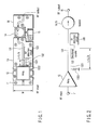
- FIG. 1 shows the layout of a microwave amplifier and an output monitor circuit as an embodiment of the output monitor circuit in a radio frequency circuit according to the present invention; and
- FIG. 2 shows the equivalent circuit of the radio-frequency circuit shown in FIG. 1.
- An embodiment of an output monitor circuit of a microwave amplifier according to the present invention will be described hereinafter with reference to FIGS. 1 and 2.
- FIG. 1 shows the layout of circuits and FIG. 2 shows the equivalent circuit of the circuits. In FIG. 1, 11 denotes an RF input terminal unit, 12 an amplifier unit in which the microwave amplifier is built, 13 an RF output monitor unit, 14 a circulator unit, 15 a terminating resistor unit, and 16 an RF output terminal unit. They are arranged on a base plate (not shown) and fixed to it with screws.
- The output end of the
amplifier unit 12 is coupled to anoutput line 131 formed in themonitor unit 13. In themonitor unit 13, acoupling line 1321 of adirectional coupler 132 is formed in close proximity to theoutput line 131 and has its one end on the RF input side connected to a terminatingresistor 1322 and its other end on the RF output side directly connected to the input of anRF detection circuit 133. The length L of thecoupling line 1321 is selected to be less than a quarter of the RF signal wavelength λ. In view of the degree of coupling, the practical length of the coupling line is of the order of λ/8. - The
output line 131 of themonitor unit 13 is connected to the signal input terminal of thecirculator unit 14, which has its one signal output end connected to the output line of the RFoutput terminal unit 16. In addition, the circulator unit has its other output terminal connected to the terminatingresistor unit 15. That is, thecirculator unit 14 functions as an isolator as indicated by the equivalent circuit of FIG. 2. For this reason, unwanted signal components reflected from the RFoutput terminal unit 16 toward thecirculator unit 14 are shunted to ground by the terminatingresistor unit 15 connected to the other output terminal of the circulator unit. Thereby, back flow of RF output to themonitor unit 13 is blocked. - That is, in the
directional coupler 132 in the RFoutput monitor unit 13, to take out RF coupled output from the side opposite to that in the conventional one, the length L of thecoupling line 1321 is set such that L < λ/4. This causes the directivity of the coupling to be lowered. RF power obtained from the RF coupled output is converted into a DC voltage in theRF detection circuit 133 to monitor the RF power. On the other hand, RF power returned from the output side is blocked by thecirculator unit 14 functioning as an isolator. The performance of the output monitor circuit which is comparable to that of the conventional one can be achieved and erroneous detection can be prevented. - According to the output monitor circuit thus configured, therefore, the RF
output monitor unit 13 can be made small in size by orienting the RF output end of the directional coupler toward the RF output side and making the length of the coupling line less than λ/4. In addition, it is not necessary to fold back of line pattern. Therefore, this also makes it possible to set the width of each of the base plates for theamplifier unit 12 and themonitor unit 13 to W as shown in FIG. 1. Moreover, RF output monitoring accuracy and device performance can be improved because back flow of unwanted signal components due to signal reflection, wrap-around, and so on is almost completely suppressed. The improved monitoring accuracy allows failure detection utilizing monitor outputs, temperature compensation, and feedback control based on level detection to be implemented with higher accuracy. - The above embodiment is configured such that the
circulator unit 14 is set on the output side of themonitor unit 13 in order to prevent back flow of unwanted signal components to the RF detection circuit. In microwave circuits used in radar equipment and so on, a circulator (or an isolator) is generally set on the output side of an amplifier. In this case, it is also possible to use that circulator as thecirculator unit 13 described above. - Although, in the embodiment described above, each of the circuit components is unitized, they may be integrated in whole or in part.
- Although the embodiment has been described as monitoring the output state of a microwave amplifier, the subject to be monitored in this invention is not limited to the microwave amplifier and the principles of the invention are applicable to any other radio-frequency circuit.
Claims (3)
- An output monitor circuit of a radio-frequency circuit (12) which outputs a radio-frequency signal of wavelength λ characterized by comprising:a directional coupler (132) having a coupling line (1321) of a length less than λ/4 coupled with an output line (131) of the radio-frequency circuit (12) and a terminating resistor (1322) connected to one end on the radio-frequency circuit side of the coupling line, a radio-frequency signal being derived from the other end of the coupling line by means of coupling between the coupling line and the output line;a detection circuit (133) which detects a radio-frequency signal derived from the directional coupler (132) to produce a monitor signal; anda back flow blocking circuit (14) which blocks signal components back flowing from the output side toward the output line (131) in a portion where there is no coupling between the output line (131) and the coupling line (1321).
- The output monitor circuit according to claim 1, characterized in that the radio-frequency circuit is a radio-frequency amplifier.
- The output monitor circuit according to claim 1, characterized in that the back flow blocking circuit (14) is a circulator which conducts a radio-frequency signal derived from the radio-frequency circuit (12) to the output line (131) to an output end and conducts signal components flowing from the output end into the circulator to ground line.
Applications Claiming Priority (1)
| Application Number | Priority Date | Filing Date | Title |
|---|---|---|---|
| JP2005365095A JP4599286B2 (en) | 2005-12-19 | 2005-12-19 | High frequency output monitor circuit device |
Publications (1)
| Publication Number | Publication Date |
|---|---|
| EP1798862A1 true EP1798862A1 (en) | 2007-06-20 |
Family
ID=37769381
Family Applications (1)
| Application Number | Title | Priority Date | Filing Date |
|---|---|---|---|
| EP06256422A Withdrawn EP1798862A1 (en) | 2005-12-19 | 2006-12-18 | Output monitor circuit of a radio transmitter |
Country Status (3)
| Country | Link |
|---|---|
| US (1) | US7904038B2 (en) |
| EP (1) | EP1798862A1 (en) |
| JP (1) | JP4599286B2 (en) |
Citations (6)
| Publication number | Priority date | Publication date | Assignee | Title |
|---|---|---|---|---|
| US5424694A (en) * | 1994-06-30 | 1995-06-13 | Alliedsignal Inc. | Miniature directional coupler |
| JP2002043957A (en) * | 2000-07-19 | 2002-02-08 | Hitachi Kokusai Electric Inc | High frequency signal transmission device |
| US20020185659A1 (en) * | 2001-04-04 | 2002-12-12 | Shuichiro Yamaguchi | Non-reciprocal circuit device |
| EP1294044A2 (en) * | 2001-09-12 | 2003-03-19 | Radio Frequency Systems, Inc. | Coplanar directional coupler for hybrid geometry |
| JP2004343419A (en) * | 2003-05-15 | 2004-12-02 | Matsushita Electric Ind Co Ltd | Directional coupler |
| US20050258917A1 (en) * | 2004-05-19 | 2005-11-24 | Xytrans, Inc. | Microstrip directional coupler |
Family Cites Families (17)
| Publication number | Priority date | Publication date | Assignee | Title |
|---|---|---|---|---|
| US4211911A (en) * | 1979-01-16 | 1980-07-08 | General Electric Company | Microwave directional coupler and detector module |
| JPS5721102A (en) * | 1980-07-14 | 1982-02-03 | Toshiba Corp | Microstrip directional coupler |
| JPH0545387A (en) * | 1991-03-27 | 1993-02-23 | Mitsubishi Electric Corp | High frequency signal power monitor circuit |
| JP3158214B2 (en) * | 1991-09-20 | 2001-04-23 | 富士通株式会社 | Semiconductor amplifier |
| JP3187662B2 (en) | 1994-08-31 | 2001-07-11 | 三菱電機株式会社 | Microwave power detection circuit |
| JPH10233607A (en) * | 1997-02-19 | 1998-09-02 | Murata Mfg Co Ltd | Directional coupler |
| JP3735199B2 (en) | 1998-04-20 | 2006-01-18 | 新日本無線株式会社 | Power combiner for high frequency power monitor |
| JP2000341145A (en) * | 1999-05-27 | 2000-12-08 | Alps Electric Co Ltd | Transmission circuit and transmitter-receiver equipped with the transmission circuit |
| JP2000341143A (en) * | 1999-05-28 | 2000-12-08 | Matsushita Electric Ind Co Ltd | Wireless circuit |
| JP2002043813A (en) * | 2000-05-19 | 2002-02-08 | Hitachi Ltd | Directional coupler, high-frequency circuit module, and wireless communication device |
| US20020113666A1 (en) * | 2000-07-04 | 2002-08-22 | Masazumi Yamazaki | Directional coupler directional coupling method |
| JP2002084112A (en) * | 2000-09-06 | 2002-03-22 | Hitachi Kokusai Electric Inc | Directional coupler for high frequency monitor |
| US6876282B2 (en) * | 2002-05-17 | 2005-04-05 | International Business Machines Corporation | Micro-electro-mechanical RF switch |
| US7512386B2 (en) * | 2003-08-29 | 2009-03-31 | Nokia Corporation | Method and apparatus providing integrated load matching using adaptive power amplifier compensation |
| US7508898B2 (en) * | 2004-02-10 | 2009-03-24 | Bitwave Semiconductor, Inc. | Programmable radio transceiver |
| WO2005114777A1 (en) * | 2004-05-21 | 2005-12-01 | Murata Manufacturing Co., Ltd. | Microstrip line type directional coupler and communication device using it |
| JP5169844B2 (en) * | 2009-01-06 | 2013-03-27 | 三菱電機株式会社 | Directional coupler |
-
2005
- 2005-12-19 JP JP2005365095A patent/JP4599286B2/en not_active Expired - Lifetime
-
2006
- 2006-12-18 EP EP06256422A patent/EP1798862A1/en not_active Withdrawn
- 2006-12-18 US US11/612,098 patent/US7904038B2/en active Active
Patent Citations (6)
| Publication number | Priority date | Publication date | Assignee | Title |
|---|---|---|---|---|
| US5424694A (en) * | 1994-06-30 | 1995-06-13 | Alliedsignal Inc. | Miniature directional coupler |
| JP2002043957A (en) * | 2000-07-19 | 2002-02-08 | Hitachi Kokusai Electric Inc | High frequency signal transmission device |
| US20020185659A1 (en) * | 2001-04-04 | 2002-12-12 | Shuichiro Yamaguchi | Non-reciprocal circuit device |
| EP1294044A2 (en) * | 2001-09-12 | 2003-03-19 | Radio Frequency Systems, Inc. | Coplanar directional coupler for hybrid geometry |
| JP2004343419A (en) * | 2003-05-15 | 2004-12-02 | Matsushita Electric Ind Co Ltd | Directional coupler |
| US20050258917A1 (en) * | 2004-05-19 | 2005-11-24 | Xytrans, Inc. | Microstrip directional coupler |
Non-Patent Citations (1)
| Title |
|---|
| CHANG C-C ET AL: "ENHANCED FORWARD COUPLING PHENOMENA BETWEEN MICROSTRIP LINES ON PERIODICALLY PATTERNED GROUND PLANE", 2001 IEEE MTT-S INTERNATIONAL MICROWAVE SYMPOSIUM DIGEST.(IMS 2001). PHOENIX, AZ, MAY 20 - 25, 2001; [IEEE MTT-S INTERNATIONAL MICROWAVE SYMPOSIUM], NEW YORK, NY : IEEE, US LNKD- DOI:10.1109/MWSYM.2001.967312, 20 May 2001 (2001-05-20), pages 2039 - 2042, XP001061192, ISBN: 978-0-7803-6538-4 * |
Also Published As
| Publication number | Publication date |
|---|---|
| US20070139260A1 (en) | 2007-06-21 |
| JP2007173956A (en) | 2007-07-05 |
| JP4599286B2 (en) | 2010-12-15 |
| US7904038B2 (en) | 2011-03-08 |
Similar Documents
| Publication | Publication Date | Title |
|---|---|---|
| JP2004173243A (en) | Front-end module and communication terminal | |
| JP6457968B2 (en) | Pulse radar device and its parts | |
| CN110429951B (en) | Radio frequency transceiver device, corresponding system and method | |
| US6556815B1 (en) | Transmitting circuit in which damage to power amplifier due to reflected wave is prevented and transmitter-receiver provided with the transmitting circuit | |
| EP4220952A1 (en) | Protection circuit for acoustic filter and power amplifier stage | |
| EP2850728B1 (en) | Integrated technique for enhanced power amplifier forward power detection | |
| US7904038B2 (en) | Output monitor circuit of radio-frequency circuit | |
| KR20070105158A (en) | Receiver protection device for time division duplex wireless communication system | |
| US10038477B2 (en) | Combined active and passive high-power RF protection circuit | |
| JPH06510176A (en) | amplitude limiter circuit | |
| US7800438B2 (en) | Bypass device for microwave amplifier unit | |
| JP4213552B2 (en) | External antenna detection circuit, wireless device and external antenna switching circuit | |
| FI94692C (en) | rADIO SET | |
| JP4286708B2 (en) | Microwave power transmitter | |
| KR100817510B1 (en) | Apparatus and method for checking the connection of antennas in wireless equipment | |
| JP2000223962A (en) | Microwave amplifier | |
| CN110994111A (en) | Standing wave detection board | |
| JP2007303862A (en) | Apparatus for detecting connection failure of coaxial cable | |
| JP6702565B2 (en) | Transceiver | |
| KR100693558B1 (en) | Power detection device using RF signal | |
| JP2005260428A (en) | Transmitter circuit | |
| KR100737334B1 (en) | Microwave Directional Detector Using Microstrip Structure | |
| JPS6159917A (en) | Transmission output switching device | |
| KR101870935B1 (en) | Multi-band return signal measurement device | |
| CN117478246A (en) | A monitoring and protection circuit and communication equipment |
Legal Events
| Date | Code | Title | Description |
|---|---|---|---|
| PUAI | Public reference made under article 153(3) epc to a published international application that has entered the european phase |
Free format text: ORIGINAL CODE: 0009012 |
|
| 17P | Request for examination filed |
Effective date: 20070109 |
|
| AK | Designated contracting states |
Kind code of ref document: A1 Designated state(s): AT BE BG CH CY CZ DE DK EE ES FI FR GB GR HU IE IS IT LI LT LU LV MC NL PL PT RO SE SI SK TR |
|
| AX | Request for extension of the european patent |
Extension state: AL BA HR MK YU |
|
| 17Q | First examination report despatched |
Effective date: 20071022 |
|
| AKX | Designation fees paid |
Designated state(s): DE FR GB |
|
| STAA | Information on the status of an ep patent application or granted ep patent |
Free format text: STATUS: THE APPLICATION IS DEEMED TO BE WITHDRAWN |
|
| 18D | Application deemed to be withdrawn |
Effective date: 20131126 |