EP1798777A2 - Reduced band gap absorber for solar cells - Google Patents
Reduced band gap absorber for solar cells Download PDFInfo
- Publication number
- EP1798777A2 EP1798777A2 EP06077166A EP06077166A EP1798777A2 EP 1798777 A2 EP1798777 A2 EP 1798777A2 EP 06077166 A EP06077166 A EP 06077166A EP 06077166 A EP06077166 A EP 06077166A EP 1798777 A2 EP1798777 A2 EP 1798777A2
- Authority
- EP
- European Patent Office
- Prior art keywords
- solar cell
- dual heterojunction
- region
- dual
- heterojunction
- Prior art date
- Legal status (The legal status is an assumption and is not a legal conclusion. Google has not performed a legal analysis and makes no representation as to the accuracy of the status listed.)
- Granted
Links
Images



Classifications
-
- H—ELECTRICITY
- H10—SEMICONDUCTOR DEVICES; ELECTRIC SOLID-STATE DEVICES NOT OTHERWISE PROVIDED FOR
- H10F—INORGANIC SEMICONDUCTOR DEVICES SENSITIVE TO INFRARED RADIATION, LIGHT, ELECTROMAGNETIC RADIATION OF SHORTER WAVELENGTH OR CORPUSCULAR RADIATION
- H10F10/00—Individual photovoltaic cells, e.g. solar cells
- H10F10/10—Individual photovoltaic cells, e.g. solar cells having potential barriers
- H10F10/17—Photovoltaic cells having only PIN junction potential barriers
-
- B—PERFORMING OPERATIONS; TRANSPORTING
- B82—NANOTECHNOLOGY
- B82Y—SPECIFIC USES OR APPLICATIONS OF NANOSTRUCTURES; MEASUREMENT OR ANALYSIS OF NANOSTRUCTURES; MANUFACTURE OR TREATMENT OF NANOSTRUCTURES
- B82Y20/00—Nanooptics, e.g. quantum optics or photonic crystals
-
- H—ELECTRICITY
- H10—SEMICONDUCTOR DEVICES; ELECTRIC SOLID-STATE DEVICES NOT OTHERWISE PROVIDED FOR
- H10F—INORGANIC SEMICONDUCTOR DEVICES SENSITIVE TO INFRARED RADIATION, LIGHT, ELECTROMAGNETIC RADIATION OF SHORTER WAVELENGTH OR CORPUSCULAR RADIATION
- H10F10/00—Individual photovoltaic cells, e.g. solar cells
- H10F10/10—Individual photovoltaic cells, e.g. solar cells having potential barriers
- H10F10/14—Photovoltaic cells having only PN homojunction potential barriers
- H10F10/142—Photovoltaic cells having only PN homojunction potential barriers comprising multiple PN homojunctions, e.g. tandem cells
-
- H—ELECTRICITY
- H10—SEMICONDUCTOR DEVICES; ELECTRIC SOLID-STATE DEVICES NOT OTHERWISE PROVIDED FOR
- H10F—INORGANIC SEMICONDUCTOR DEVICES SENSITIVE TO INFRARED RADIATION, LIGHT, ELECTROMAGNETIC RADIATION OF SHORTER WAVELENGTH OR CORPUSCULAR RADIATION
- H10F10/00—Individual photovoltaic cells, e.g. solar cells
- H10F10/10—Individual photovoltaic cells, e.g. solar cells having potential barriers
- H10F10/16—Photovoltaic cells having only PN heterojunction potential barriers
- H10F10/161—Photovoltaic cells having only PN heterojunction potential barriers comprising multiple PN heterojunctions, e.g. tandem cells
-
- H—ELECTRICITY
- H10—SEMICONDUCTOR DEVICES; ELECTRIC SOLID-STATE DEVICES NOT OTHERWISE PROVIDED FOR
- H10F—INORGANIC SEMICONDUCTOR DEVICES SENSITIVE TO INFRARED RADIATION, LIGHT, ELECTROMAGNETIC RADIATION OF SHORTER WAVELENGTH OR CORPUSCULAR RADIATION
- H10F10/00—Individual photovoltaic cells, e.g. solar cells
- H10F10/10—Individual photovoltaic cells, e.g. solar cells having potential barriers
- H10F10/16—Photovoltaic cells having only PN heterojunction potential barriers
- H10F10/163—Photovoltaic cells having only PN heterojunction potential barriers comprising only Group III-V materials, e.g. GaAs/AlGaAs or InP/GaInAs photovoltaic cells
-
- H—ELECTRICITY
- H10—SEMICONDUCTOR DEVICES; ELECTRIC SOLID-STATE DEVICES NOT OTHERWISE PROVIDED FOR
- H10F—INORGANIC SEMICONDUCTOR DEVICES SENSITIVE TO INFRARED RADIATION, LIGHT, ELECTROMAGNETIC RADIATION OF SHORTER WAVELENGTH OR CORPUSCULAR RADIATION
- H10F10/00—Individual photovoltaic cells, e.g. solar cells
- H10F10/10—Individual photovoltaic cells, e.g. solar cells having potential barriers
- H10F10/19—Photovoltaic cells having multiple potential barriers of different types, e.g. tandem cells having both PN and PIN junctions
-
- H—ELECTRICITY
- H10—SEMICONDUCTOR DEVICES; ELECTRIC SOLID-STATE DEVICES NOT OTHERWISE PROVIDED FOR
- H10F—INORGANIC SEMICONDUCTOR DEVICES SENSITIVE TO INFRARED RADIATION, LIGHT, ELECTROMAGNETIC RADIATION OF SHORTER WAVELENGTH OR CORPUSCULAR RADIATION
- H10F77/00—Constructional details of devices covered by this subclass
- H10F77/10—Semiconductor bodies
- H10F77/14—Shape of semiconductor bodies; Shapes, relative sizes or dispositions of semiconductor regions within semiconductor bodies
-
- H—ELECTRICITY
- H10—SEMICONDUCTOR DEVICES; ELECTRIC SOLID-STATE DEVICES NOT OTHERWISE PROVIDED FOR
- H10F—INORGANIC SEMICONDUCTOR DEVICES SENSITIVE TO INFRARED RADIATION, LIGHT, ELECTROMAGNETIC RADIATION OF SHORTER WAVELENGTH OR CORPUSCULAR RADIATION
- H10F77/00—Constructional details of devices covered by this subclass
- H10F77/10—Semiconductor bodies
- H10F77/14—Shape of semiconductor bodies; Shapes, relative sizes or dispositions of semiconductor regions within semiconductor bodies
- H10F77/146—Superlattices; Multiple quantum well structures
-
- Y—GENERAL TAGGING OF NEW TECHNOLOGICAL DEVELOPMENTS; GENERAL TAGGING OF CROSS-SECTIONAL TECHNOLOGIES SPANNING OVER SEVERAL SECTIONS OF THE IPC; TECHNICAL SUBJECTS COVERED BY FORMER USPC CROSS-REFERENCE ART COLLECTIONS [XRACs] AND DIGESTS
- Y02—TECHNOLOGIES OR APPLICATIONS FOR MITIGATION OR ADAPTATION AGAINST CLIMATE CHANGE
- Y02E—REDUCTION OF GREENHOUSE GAS [GHG] EMISSIONS, RELATED TO ENERGY GENERATION, TRANSMISSION OR DISTRIBUTION
- Y02E10/00—Energy generation through renewable energy sources
- Y02E10/50—Photovoltaic [PV] energy
- Y02E10/544—Solar cells from Group III-V materials
-
- Y—GENERAL TAGGING OF NEW TECHNOLOGICAL DEVELOPMENTS; GENERAL TAGGING OF CROSS-SECTIONAL TECHNOLOGIES SPANNING OVER SEVERAL SECTIONS OF THE IPC; TECHNICAL SUBJECTS COVERED BY FORMER USPC CROSS-REFERENCE ART COLLECTIONS [XRACs] AND DIGESTS
- Y02—TECHNOLOGIES OR APPLICATIONS FOR MITIGATION OR ADAPTATION AGAINST CLIMATE CHANGE
- Y02E—REDUCTION OF GREENHOUSE GAS [GHG] EMISSIONS, RELATED TO ENERGY GENERATION, TRANSMISSION OR DISTRIBUTION
- Y02E10/00—Energy generation through renewable energy sources
- Y02E10/50—Photovoltaic [PV] energy
- Y02E10/548—Amorphous silicon PV cells
Definitions
- the present invention relates generally to solar cells, and, in particular, to a method, apparatus, and article of manufacture of a reduced band gap absorber for solar cells.
- Solar energy created through the photovoltaic effect is the main source of power for most commercial and government spacecraft.
- the amount of power generated by an array of solar cells is limited by the launch volume and launch weight. These restrictions limit the capability of the spacecraft.
- any terrestrial solar cells are limited by the size of an array that can be installed in a given installation.
- the power per unit area for the solar cell array must be increased.
- Increasing the efficiency of the solar cell is of primary importance for enabling near-earth missions.
- the dominant solar cell technology for this application is a combination of subcells comprising Gallium Indium Phosphide (GaInP), Gallium Arsenide (GaAs), and Germanium (Ge), which is typically called a triple-junction, or "3J", device.
- the current best efficiency of a 3J device at the Beginning Of Life (BOL) is 28.6%, which degrades over time to an End Of Life (EOL) final percentage.
- Solar cells used in space must survive for up to fifteen years in an environment rich in atomic oxygen and energetic sub-atomic particles, which degrades the solar cells significantly.
- the general objective of any change in the design of solar cells is to reduce the cost of the device, the BOL efficiency, or to decrease the rate of degradation such that the EOL efficiency is higher as well.
- MQW multiple quantum-well
- a method in accordance with the present invention comprises growing a base material for a solar cell, growing at least one dual heterojunction on the base material, and growing an emitter on the at least one dual heterojunction.
- Such a method further optionally includes the base, emitter, and at least one dual heterojunction being in a top cell of a triple-junction solar cell, the at least one dual heterojunction being at least 200 angstroms in thickness, the at least one dual heterojunction being a stack of alternating low bandgap materials and barrier materials, the at least one dual heterojunction being contained within a depletion region created by the base material and the emitter, and a material for the low bandgap material being gallium arsenide.
- An apparatus in acccordance with the present invention comprises a substrate, and a first subcell, coupled to the substrate, wherein the first subcell comprises a base region, coupled to the substrate, an emitter region, and at least one dual heterojunction, coupled between the base region and the emitter region, wherein the at least one dual heterojunction has a lower bandgap than the emitter region.
- Such an apparatus further optionally includes a second subcell, coupled between the substrate and the first subcell, the at least one dual heterojunction being at least 200 angstroms in thickness, the at least one dual heterojunction being a stack of alternating low bandgap material and barrier materials, the at least one dual heterojunction being contained within a depletion region created by the emitter region and the base region, and a material for the dual heterojunction being one or any alloy combination (continuous or digital) of: GaAs, GaInAs, GaInAsN, GaInAsNSb, GaInP, GaPN, GaInPN, InPN, InN, InNAs, GaInPAsN, InP, AlGaInP, GaAsP, AlGaAs, GaInAsP, GaSb, InSb, InAs, Ge, SiGe, SiGeC, SiGeSn, ZnGeAs, ZnGeSiAs, CuAlGaInS, CuAlGaInS
- An alternate embodiment of the present invention comprises a dual heterojunction region of at least 200 angstroms thickness, the dual heterojunction region being contained within a depletion region of the solar cell, such that the dual heterojunction region generates additional current in the solar cell by absorbing incident light within the dual heterojunction region.
- Such an embodiment optionally further includes the dual heterojunction region being in a top subcell of a multijunction solar cell.
- the current 3J concept of GaInP/Ga(In)As/Ge is not optimal. This occurs because the layers are grown one on top of another epitaxially, and, to perform such growth, the lattice spacing of the materials must be very similar. The lattice constants for the material restricts the choices of materials available for cell combinations. Since the cells are electrically connected in series, the cell producing the lowest current will limit the current produced by the entire cell stack. As such, the current produced by each of the subcells should be approximately the same, or the excess current produced generates waste heat.
- the natural GaInP material in the stack produces too much current compared to the Ga(In)As subcell.
- the GaInP subcell is thinned to balance the current.
- the optimal bandgap for a balanced current from the GaInP subcell is 2.0 eV.
- GaInP Aluminum Gallium Indium Phosphide, or AlGaInP
- GaAs Gallium Indium Arsenide, or GaInAs
- the thicker the layer the more expensive it is to produce.
- the device will weigh more, and will be more susceptible to degradation due to larger layers having a larger radiation exposure.
- To create a bandgap of 2.0 eV in AlGaInP approximately four times as much material must be used to balance the current with the middle cell. As can be seen, this increases cost, weight, and decreases EOL efficiency.
- MQW approaches have thinned the upper layers somewhat, but the quantum well layers now must be extremely thin. Thinner layers absorb less light, and, as such, many quantum wells must be employed to allow enough light to be absorbed to generate enough gain from the device. Typically, between 10 and 100 wells of an average thickness of 75 to 100 angstroms each are used.
- the advantage of quantum well generation of current is that the quantum confinement raises the allowed states in the well above the bandgap of the material, which usually provides for lower dark currents and a higher voltage for the quantum well compared to the bulk material.
- the elevated energy of the allowed states results fewer long-wavelength photons that can be absorbed and lower current density, imposing a penalty for cell performance in the multiple quantum well approach.
- the MQW approach is typically accompanied by a loss in open circuit voltage, as well as additional costs to create the large number of very thin layers.
- the present invention uses a small number of lower bandgap regions in the intrinsic or depletion region of one or more of the subcells of the solar cell.
- the regions are sufficiently thick so as not to be quantum well in nature, and relatively shallow such that generated carriers may easily escape.
- the required energy profile or substructure of the low band gap absorber region is arbitrary, which allows for lower tolerances on the fabrication of devices made using the present invention.
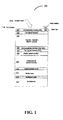
- FIG. 1 illustrates a triple junction solar cell of the related art.
- Top subcell 105 is typically an AlGaInP subcell, which has a Back Surface Field (BSF) 106.
- Top Tunnel Junction (TJ1) 107 is resident between the top cell 105 and the middle subcell window 108.
- Middle subcell 109 is typically GaInAs, or GaSbAs, which has a Tunnel Junction (TJ2) 110 between subcell 109 and a buffer layer 111.
- a nucleation layer 112 is placed between buffer layer 111 and the substrate 113, which is typically Germanium.
- Incident light 114 strikes top surface 116 and is converted to electrical voltage and current in the top subcell 105, middle subcell 109, and the substrate 113.
- the top subcell 105, middle subcell 109, and substrate 113 each typically convert different wavelengths of light into electrical energy, and the subcells 105 and 109 and substrate 113 are chosen such that the wavelengths of light overlap to some degree to increase the efficiency of the solar cell 100.
- FIG. 2 illustrates a subcell in a triple junction solar cell of the related art.
- Subcell 200 shows an upper structure 201, a subcell window 202, an emitter 203, an intrinsic or depletion region 204, a base region 205, a BSF 206, and a lower structure 207. Although shown as an n-type on p-type subcell 200, a p-type on n-type subcell 200 can be made without departing from the scope of the present invention.
- FIG. 2 illustrates a typical top subcell 105, or middle subcell 109, with the adjoining subcell windows, BSF, etc. used for such subcells in a solar cell 100.
- top subcell 105 increases exponentially for top subcell 105. This effect occurs because the solar cell 100 is connected in series.
- the lowest current generating portion of solar cell 100 i.e., one of subcell 105, 109, and substrate 113, limits the current produced for the overall solar cell 100.
- the top subcell 105 is the limiting factor in terms of current generation, and, as such, the top subcell 105 must be made thicker in height 208.
- 2.0eV is the optimal bandgap by theory for top subcell 105. To produce a 2.0 eV top subcell 105, it must be thicker, which takes longer to grow and thus becomes more costly.
- thicker cells are more easily degraded by space environments, which depend on minority carrier travel distance through the cell. The thicker the cell, the farther minority carriers must travel. A degraded lattice structure prevents minority carriers from travelling very far without scattering or recombination.
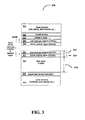
- FIG. 3 illustrates a subcell in accordance of the present invention.
- Subcell 300 is shown with an upper structure 310, subcell window 302, emitter 303, low bandgap material 304, barrier material 305, low bandgap material 306, barrier material 307, base region 308, BSF 309, and lower structure 310.
- the present invention uses a stack of low band gap materials in the depletion region between emitter 303 and base 308 to build up the 2.0 eV top subcell (or any other subcell in solar cell 300).
- each pair of low bandgap material 304/barrier material 306 is typically referred to as a Dual Heterostructure (DH).
- Each low band gap material 304, 306 is a well layer, where w 312 is the depth of the well.
- w 312 combined with b 314 is typically less than 200 angstroms.
- w 312 combined with b 314 is greater than 200 angstroms, and typically a few hundred angstroms, because the wells are not sufficiently thin to entrap a generated electron and change its quantum character, thus, there is no quantum confinement of generated electrons in specific energy states in layers 304 and 306.
- the present invention allows for the building of low band-gap regions (e.g.
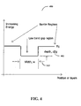
- FIG. 4 illustrates a schematic of a well of lower band gap enclosed by regions of higher band gap material as used in the present invention.
- the width w 312 of the absorber region (low band gap regions 304 and 306) has a depth 402. This depth can represent the difference to either the conduction band or the valence band of the material to show the confinement in the absorber regions 304 and 306.
- the thickness is about 200 angstroms. At lower thicknesses, the DH begins acting like a quantum well, with the energy level of the lower bound state in the well becoming substantially higher than be bandgap of the well material.
- the influence of the quantum effect on the lowest energy transition in the well becomes indistinguishable from the bandgap, such that the lower bound state is within a fraction of the available thermal energy.
- the quasi-Fermi levels in the depletion region may collapse to that of the low bandgap material and there will be a voltage drop in the open circuit voltage of the device 300.
- the low bandgap regions (304, 306 and the barrier materials 305, 307) must be fully contained within the depletion region created by emitter 303 and base region 308.
- the depletion region is dependent upon the dopant densities of emitter 303 and base 308; as long as the DH pairs are located within the depletion region, the electric field in the depletion region accelerates the charges out of the DH and aids in their collection in the emitter 303 and base 308. Without the electric field, the generated carriers will remain in the DH and generate only dark current, which lowers the voltage and does not contribute to the current generated by the device 300.
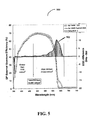
- FIG. 5 illustrates an example of the spectral response of an AlGaInP top subcell with and without the dual heterostructures of the present invention.
- Chart 500 shows the quantum efficiency on the x axis versus wavelength on the y-axis, with squares representing the efficiency of a related art 3J cell, and circles representing the efficiency of a 3Jcell with the Dual Heterostructures of the present invention.
- the DHs used in the structure were 250 angstroms thick, and there were three periods of DHs used in this experiment.
- the solid line 502 shows the difference in efficiency of the device with the DHs present versus the related art 3J solar cell.
- the related art solar cell has an AlGaInP top subcell (shown as element 105 in FIG. 1) having a bandgap of 1.98eV and the base thickness (shown as base 205 in FIG. 2) having a thickness 208 of 7000 angstroms. Note that there is not a change in absorption coefficient in changing to a quantum state with an inflection or step function density of states, and, as such, the DHs are not acting as quantum wells. There is a net gain of 0.550 mA/cm2 for the addition of the absorber region. This net gain came at the addition of approximately 1000 angstroms of thickness.
- the present invention saves a net of approximately 4000 to 6000 angstroms of material. Since this material accounts for approximately 50 percent of the growth cost, the savings is approximately 25 percent of the total growth cost to produce a 1.98 eV AlGaInP top subcell 300 over a similar top subcell 200.
- FIGS. 6 and 7 illustrate comparisons between a standard cell, a MQW cell, and a DH cell of the present invention.
- FIG. 6 shows the open circuit voltage for a standard cell 600, for an MQW cell 602, and a DH cell 604.
- FIG. 7 shows the spectral response current for a standard cell 700, for an MQW cell 702, and a DH cell 704.
- the MQW cell 704 has an increase of 0.46 mA average over the standard cell 700, and the DH cell 704 has a 0.42 mA average gain over the standard cell 700.
- FIG. 8 is a flowchart illustrating the steps of the present invention.
- Box 800 illustrates growing a base material for a solar cell.
- Box 802 illustrates growing at least one dual heterojunction on the base material.
- Box 804 illustrates growing an emitter on the at least one dual heterojunction.
- embodiments of the invention provide methods and apparatuses for a dual heterojunction multijunction solar cell.
- a method in accordance with the present invention comprises growing a base material for a solar cell, growing at least one dual heterojunction on the base material, and growing an emitter on the at least one dual heterojunction.
- Such a method further optionally includes the base, emitter, and at least one dual heterojunction being in a top cell of a triple junction solar cell, the at least one dual heterojunction being at least 200 angstroms in thickness, the at least one dual heterojunction being a stack of alternating low bandgap materials and barrier materials, the at least one dual heterojunction being contained within a depletion region created by the base material and the emitter, and a material for the low bandgap material being one or any alloy combination (continuous or digital) of: GaAs, GaInAs, GaInAsN, GaInAsNSb, GaInP, GaPN, GaInPN, InPN, InN, InNAs, GaInPAsN, InP, AlGaInP, GaAsP, AlGaAs, GaInAsP, GaSb, InSb, InAs, Ge, SiGe, SiGeC, SiGeSn, ZnGeAs, ZnGeSiAs, Cu
- An apparatus in acccordance with the present invention comprises a substrate, and a first subcell, coupled to the substrate, wherein the first subcell comprises a base region, coupled to the substrate, an emitter region, and at least one dual heterojunction, coupled between the base region and the emitter region, wherein the at least one dual heterojunction has a lower bandgap than the emitter region.
- Such an apparatus further optionally includes a second subcell, coupled between the substrate and the first subcell, the at least one dual heterojunction being at least 200 angstroms in thickness, the at least one dual heterojunction being a stack of alternating low bandgap material and barrier materials, the at least one dual heterojunction being contained within a depletion region created by the emitter region and the base region, and a material for the dual heterojunction being gallium arsenide.
- An alternate embodiment of the present invention comprises a dual heterojunction region of at least 200 angstroms thickness, the dual heterojunction region being contained within a depletion region of the solar cell, such that the dual heterojunction region generates additional current in the solar cell by absorbing incident light within the dual heterojunction region.
- Such an embodiment optionally further includes the dual heterojunction region being in a top subcell of a multijunction solar cell.
Landscapes
- Engineering & Computer Science (AREA)
- Chemical & Material Sciences (AREA)
- Nanotechnology (AREA)
- Life Sciences & Earth Sciences (AREA)
- Physics & Mathematics (AREA)
- Biophysics (AREA)
- Optics & Photonics (AREA)
- Crystallography & Structural Chemistry (AREA)
- Photovoltaic Devices (AREA)
- Sustainable Energy (AREA)
- Sustainable Development (AREA)
Abstract
Description
- The present invention relates generally to solar cells, and, in particular, to a method, apparatus, and article of manufacture of a reduced band gap absorber for solar cells.
- Solar energy created through the photovoltaic effect is the main source of power for most commercial and government spacecraft. The amount of power generated by an array of solar cells is limited by the launch volume and launch weight. These restrictions limit the capability of the spacecraft. Similarly, any terrestrial solar cells are limited by the size of an array that can be installed in a given installation.
- To be able to increase payload capability, or power delivery capability, the power per unit area for the solar cell array must be increased. Increasing the efficiency of the solar cell is of primary importance for enabling near-earth missions. The dominant solar cell technology for this application is a combination of subcells comprising Gallium Indium Phosphide (GaInP), Gallium Arsenide (GaAs), and Germanium (Ge), which is typically called a triple-junction, or "3J", device.
- The current best efficiency of a 3J device at the Beginning Of Life (BOL) is 28.6%, which degrades over time to an End Of Life (EOL) final percentage. Solar cells used in space must survive for up to fifteen years in an environment rich in atomic oxygen and energetic sub-atomic particles, which degrades the solar cells significantly. The general objective of any change in the design of solar cells is to reduce the cost of the device, the BOL efficiency, or to decrease the rate of degradation such that the EOL efficiency is higher as well.
- Several approaches have been used to try to make solar cells more efficient or less costly. One approach is to use a multiple quantum-well (MQW) appraoach, which makes the efficiency go up but also makes the cells much more expensive because of the tolerances required to make an MQW structure. Other approaches use layer thickening, additional subcell structures, or mismatch of the subcell materials, each of which adds to the cost as well as the weight of the cell, limiting the usefulness of such approaches.
- It can be seen, then, that there is a need in the art for more efficient solar cells.
- To minimize the limitations in the prior art, and to minimize other limitations that will become apparent upon reading and understanding the present specification, the present invention provides methods and apparatuses for a dual heterojunction multijunction solar cell. A method in accordance with the present invention comprises growing a base material for a solar cell, growing at least one dual heterojunction on the base material, and growing an emitter on the at least one dual heterojunction.
- Such a method further optionally includes the base, emitter, and at least one dual heterojunction being in a top cell of a triple-junction solar cell, the at least one dual heterojunction being at least 200 angstroms in thickness, the at least one dual heterojunction being a stack of alternating low bandgap materials and barrier materials, the at least one dual heterojunction being contained within a depletion region created by the base material and the emitter, and a material for the low bandgap material being gallium arsenide.
- An apparatus in acccordance with the present invention comprises a substrate, and a first subcell, coupled to the substrate, wherein the first subcell comprises a base region, coupled to the substrate, an emitter region, and at least one dual heterojunction, coupled between the base region and the emitter region, wherein the at least one dual heterojunction has a lower bandgap than the emitter region.
- Such an apparatus further optionally includes a second subcell, coupled between the substrate and the first subcell, the at least one dual heterojunction being at least 200 angstroms in thickness, the at least one dual heterojunction being a stack of alternating low bandgap material and barrier materials, the at least one dual heterojunction being contained within a depletion region created by the emitter region and the base region, and a material for the dual heterojunction being one or any alloy combination (continuous or digital) of: GaAs, GaInAs, GaInAsN, GaInAsNSb, GaInP, GaPN, GaInPN, InPN, InN, InNAs, GaInPAsN, InP, AlGaInP, GaAsP, AlGaAs, GaInAsP, GaSb, InSb, InAs, Ge, SiGe, SiGeC, SiGeSn, ZnGeAs, ZnGeSiAs, CuAlGaInS, CuAlGaInSe, as long as the alloy is of lower band gap than the host surrounding barrier layers and/or base/emitter material(s).
- An alternate embodiment of the present invention comprises a dual heterojunction region of at least 200 angstroms thickness, the dual heterojunction region being contained within a depletion region of the solar cell, such that the dual heterojunction region generates additional current in the solar cell by absorbing incident light within the dual heterojunction region.
- Such an embodiment optionally further includes the dual heterojunction region being in a top subcell of a multijunction solar cell.
- Referring now to the drawings in which like reference numbers represent corresponding parts throughout:
- FIG. 1 illustrates a triple junction solar cell of the related art;
- FIG. 2 illustrates a subcell in a triple junction solar cell of the related art;
- FIG. 3 illustrates a subcell in accordance of the present invention;
- FIG. 4 illustrates a schematic of a well of lower band gap enclosed by regions of higher band gap material as used in the present invention;
- FIG. 5 illustrates an example of the spectral response of an AlGaInP top subcell with and without the dual heterostructures of the present invention;
- FIGS. 6 and 7 illustrate comparisons between a standard cell, a MQW cell, and a DH cell of the present invention; and
- FIG. 8 is a flowchart illustrating the steps of the present invention.
- In the following description, reference is made to the accompanying drawings which form a part hereof, and which is shown, by way of illustration, several embodiments of the present invention. It is understood that other embodiments may be utilized and structural changes may be made without departing from the scope of the present invention.
- The current 3J concept of GaInP/Ga(In)As/Ge is not optimal. This occurs because the layers are grown one on top of another epitaxially, and, to perform such growth, the lattice spacing of the materials must be very similar. The lattice constants for the material restricts the choices of materials available for cell combinations. Since the cells are electrically connected in series, the cell producing the lowest current will limit the current produced by the entire cell stack. As such, the current produced by each of the subcells should be approximately the same, or the excess current produced generates waste heat.
- The natural GaInP material in the stack produces too much current compared to the Ga(In)As subcell. Typically, the GaInP subcell is thinned to balance the current. The optimal bandgap for a balanced current from the GaInP subcell is 2.0 eV.
- To balance the current in the top and middle subcells of a 3J solar cell, there must be relatively thick layers of GaInP (usually Aluminum Gallium Indium Phosphide, or AlGaInP) and GaAs (usually Gallium Indium Arsenide, or GaInAs). Costwise, the thicker the layer, the more expensive it is to produce. Further, the device will weigh more, and will be more susceptible to degradation due to larger layers having a larger radiation exposure. To create a bandgap of 2.0 eV in AlGaInP, approximately four times as much material must be used to balance the current with the middle cell. As can be seen, this increases cost, weight, and decreases EOL efficiency.
- MQW approaches have thinned the upper layers somewhat, but the quantum well layers now must be extremely thin. Thinner layers absorb less light, and, as such, many quantum wells must be employed to allow enough light to be absorbed to generate enough gain from the device. Typically, between 10 and 100 wells of an average thickness of 75 to 100 angstroms each are used. The advantage of quantum well generation of current is that the quantum confinement raises the allowed states in the well above the bandgap of the material, which usually provides for lower dark currents and a higher voltage for the quantum well compared to the bulk material. However, the elevated energy of the allowed states results fewer long-wavelength photons that can be absorbed and lower current density, imposing a penalty for cell performance in the multiple quantum well approach. Moreover, the MQW approach is typically accompanied by a loss in open circuit voltage, as well as additional costs to create the large number of very thin layers.
- The present invention uses a small number of lower bandgap regions in the intrinsic or depletion region of one or more of the subcells of the solar cell. The regions are sufficiently thick so as not to be quantum well in nature, and relatively shallow such that generated carriers may easily escape. The required energy profile or substructure of the low band gap absorber region is arbitrary, which allows for lower tolerances on the fabrication of devices made using the present invention.
- FIG. 1 illustrates a triple junction solar cell of the related art.
-
Cell 100 has regions wheremetal gridline 102 and a GaAscap 102 cover the cell, and an Anti-Reflective (A/R)coating 103 covering thetop subcell window 104.Top subcell 105 is typically an AlGaInP subcell, which has a Back Surface Field (BSF) 106. Top Tunnel Junction (TJ1) 107 is resident between thetop cell 105 and themiddle subcell window 108.Middle subcell 109 is typically GaInAs, or GaSbAs, which has a Tunnel Junction (TJ2) 110 betweensubcell 109 and abuffer layer 111. A nucleation layer 112 is placed betweenbuffer layer 111 and thesubstrate 113, which is typically Germanium. -
Incident light 114 strikestop surface 116 and is converted to electrical voltage and current in thetop subcell 105,middle subcell 109, and thesubstrate 113. Thetop subcell 105,middle subcell 109, andsubstrate 113 each typically convert different wavelengths of light into electrical energy, and the subcells 105 and 109 andsubstrate 113 are chosen such that the wavelengths of light overlap to some degree to increase the efficiency of thesolar cell 100. - FIG. 2 illustrates a subcell in a triple junction solar cell of the related art.
-
Subcell 200 shows anupper structure 201, asubcell window 202, anemitter 203, an intrinsic ordepletion region 204, abase region 205, aBSF 206, and alower structure 207. Although shown as an n-type on p-type subcell 200, a p-type on n-type subcell 200 can be made without departing from the scope of the present invention. FIG. 2 illustrates a typicaltop subcell 105, ormiddle subcell 109, with the adjoining subcell windows, BSF, etc. used for such subcells in asolar cell 100. - The problem with the related art is that
height h 208 ofbase region 205 increases exponentially fortop subcell 105. This effect occurs because thesolar cell 100 is connected in series. The lowest current generating portion ofsolar cell 100, i.e., one ofsubcell substrate 113, limits the current produced for the overallsolar cell 100. Thetop subcell 105 is the limiting factor in terms of current generation, and, as such, thetop subcell 105 must be made thicker inheight 208. 2.0eV is the optimal bandgap by theory fortop subcell 105. To produce a 2.0eV top subcell 105, it must be thicker, which takes longer to grow and thus becomes more costly. Further, these thicker cells are more easily degraded by space environments, which depend on minority carrier travel distance through the cell. The thicker the cell, the farther minority carriers must travel. A degraded lattice structure prevents minority carriers from travelling very far without scattering or recombination. - FIG. 3 illustrates a subcell in accordance of the present invention.
-
Subcell 300 is shown with anupper structure 310,subcell window 302,emitter 303,low bandgap material 304,barrier material 305,low bandgap material 306,barrier material 307,base region 308,BSF 309, andlower structure 310. Rather than a singleintrinsic region 204 as shown in FIG. 2, the present invention uses a stack of low band gap materials in the depletion region betweenemitter 303 andbase 308 to build up the 2.0 eV top subcell (or any other subcell in solar cell 300). There can be a larger or smaller number of lowband gap materials typical thickness w 312, and a larger or smaller number ofbarrier material regions typical thickness b 314, resident on top ofbase 308 having athickness h 316. Each pair oflow bandgap material 304/barrier material 306 is typically referred to as a Dual Heterostructure (DH). - Each low
band gap material w 312 is the depth of the well. For quantum well structures,w 312 combined withb 314 is typically less than 200 angstroms. However, in the present invention,w 312 combined withb 314 is greater than 200 angstroms, and typically a few hundred angstroms, because the wells are not sufficiently thin to entrap a generated electron and change its quantum character, thus, there is no quantum confinement of generated electrons in specific energy states inlayers emitter 303 andbase 308, where these low band gap regions absorb light below the bandgap of thehigher bandgap base 308 material. The current that is produced by generating electron-hole pairs as carriers, which are then swept from the depletion region (where layers 304-307 are) and collected at the higher band-gap emitter 303 andbase 308 materials. - FIG. 4 illustrates a schematic of a well of lower band gap enclosed by regions of higher band gap material as used in the present invention.
- The
width w 312 of the absorber region (lowband gap regions 304 and 306) has adepth 402. This depth can represent the difference to either the conduction band or the valence band of the material to show the confinement in theabsorber regions device 300. Further, the low bandgap regions (304, 306 and thebarrier materials 305, 307) must be fully contained within the depletion region created byemitter 303 andbase region 308. The depletion region is dependent upon the dopant densities ofemitter 303 andbase 308; as long as the DH pairs are located within the depletion region, the electric field in the depletion region accelerates the charges out of the DH and aids in their collection in theemitter 303 andbase 308. Without the electric field, the generated carriers will remain in the DH and generate only dark current, which lowers the voltage and does not contribute to the current generated by thedevice 300. - FIG. 5 illustrates an example of the spectral response of an AlGaInP top subcell with and without the dual heterostructures of the present invention.
- Chart 500 shows the quantum efficiency on the x axis versus wavelength on the y-axis, with squares representing the efficiency of a related art 3J cell, and circles representing the efficiency of a 3Jcell with the Dual Heterostructures of the present invention. The DHs used in the structure were 250 angstroms thick, and there were three periods of DHs used in this experiment. Note that the
solid line 502 shows the difference in efficiency of the device with the DHs present versus the related art 3J solar cell. - The related art solar cell has an AlGaInP top subcell (shown as
element 105 in FIG. 1) having a bandgap of 1.98eV and the base thickness (shown asbase 205 in FIG. 2) having athickness 208 of 7000 angstroms. Note that there is not a change in absorption coefficient in changing to a quantum state with an inflection or step function density of states, and, as such, the DHs are not acting as quantum wells. There is a net gain of 0.550 mA/cm2 for the addition of the absorber region. This net gain came at the addition of approximately 1000 angstroms of thickness. To achieve a similar gain by traditional methods, eight quantum wells of 90 angstroms each could be added, or thebase layer 205 could be thickened by about 5000 to 7000 angstroms of thickness. Therefore, the present invention saves a net of approximately 4000 to 6000 angstroms of material. Since this material accounts for approximately 50 percent of the growth cost, the savings is approximately 25 percent of the total growth cost to produce a 1.98 eVAlGaInP top subcell 300 over a similartop subcell 200. - FIGS. 6 and 7 illustrate comparisons between a standard cell, a MQW cell, and a DH cell of the present invention.
- FIG. 6 shows the open circuit voltage for a
standard cell 600, for anMQW cell 602, and aDH cell 604. The average of 1.527 Volts for astandard cell 600, 1.517 Volts for anMQW cell 602, and 1.516 Volts for aDH cell 604 of the present invention, along with the error bars, show that there is no degradation in open circuit voltage for the DH approach. - FIG. 7 shows the spectral response current for a
standard cell 700, for anMQW cell 702, and aDH cell 704. TheMQW cell 704 has an increase of 0.46 mA average over thestandard cell 700, and theDH cell 704 has a 0.42 mA average gain over thestandard cell 700. - FIG. 8 is a flowchart illustrating the steps of the present invention.
-
Box 800 illustrates growing a base material for a solar cell. -
Box 802 illustrates growing at least one dual heterojunction on the base material. -
Box 804 illustrates growing an emitter on the at least one dual heterojunction. - In summary, embodiments of the invention provide methods and apparatuses for a dual heterojunction multijunction solar cell. A method in accordance with the present invention comprises growing a base material for a solar cell, growing at least one dual heterojunction on the base material, and growing an emitter on the at least one dual heterojunction.
- Such a method further optionally includes the base, emitter, and at least one dual heterojunction being in a top cell of a triple junction solar cell, the at least one dual heterojunction being at least 200 angstroms in thickness, the at least one dual heterojunction being a stack of alternating low bandgap materials and barrier materials, the at least one dual heterojunction being contained within a depletion region created by the base material and the emitter, and a material for the low bandgap material being one or any alloy combination (continuous or digital) of: GaAs, GaInAs, GaInAsN, GaInAsNSb, GaInP, GaPN, GaInPN, InPN, InN, InNAs, GaInPAsN, InP, AlGaInP, GaAsP, AlGaAs, GaInAsP, GaSb, InSb, InAs, Ge, SiGe, SiGeC, SiGeSn, ZnGeAs, ZnGeSiAs, CuAlGaInS, CuAlGaInSe, as long as the alloy is of lower band gap than the host surrounding barrier layers and/or base/emitter material(s).
- An apparatus in acccordance with the present invention comprises a substrate, and a first subcell, coupled to the substrate, wherein the first subcell comprises a base region, coupled to the substrate, an emitter region, and at least one dual heterojunction, coupled between the base region and the emitter region, wherein the at least one dual heterojunction has a lower bandgap than the emitter region.
- Such an apparatus further optionally includes a second subcell, coupled between the substrate and the first subcell, the at least one dual heterojunction being at least 200 angstroms in thickness, the at least one dual heterojunction being a stack of alternating low bandgap material and barrier materials, the at least one dual heterojunction being contained within a depletion region created by the emitter region and the base region, and a material for the dual heterojunction being gallium arsenide.
- An alternate embodiment of the present invention comprises a dual heterojunction region of at least 200 angstroms thickness, the dual heterojunction region being contained within a depletion region of the solar cell, such that the dual heterojunction region generates additional current in the solar cell by absorbing incident light within the dual heterojunction region.
- Such an embodiment optionally further includes the dual heterojunction region being in a top subcell of a multijunction solar cell.
- The foregoing description of the preferred embodiment of the invention has been presented for the purposes of illustration and description. It is not intended to be exhaustive or to limit the invention to the precise form disclosed. Many modifications and variations are possible in light of the above teaching. It is intended that the scope of the invention be limited not by this detailed description, but rather by the claims appended hereto and the equivalents thereof.
Claims (11)
- A method for creating a dual heterojunction multijunction solar cell, comprising:growing a base material for a solar cell;growing at least one dual heterojunction on the base material; andgrowing an emitter on the at least one dual heterojunction.
- The method of claim 1, wherein the base, emitter, and at least one dual heterojunction are in a top cell of a triple junction solar cell.
- The method of claim 1 or 2, wherein a material for the low bandgap material is one or any alloy combination (continuous or digital) of: GaAs, GaInAs, GaInAsN, GaInAsNSb, GaInP, GaPN, GaInPN, InPN, InN, InNAs, GaInPAsN, InP, AlGaInP, GaAsP, AlGaAs, GaInAsP, GaSb, InSb, InAs, Ge, SiGe, SiGeC, SiGeSn, ZnGeAs, ZnGeSiAs, CuAlGaInS, CuAlGaInSe, as long as the alloy is of lower band gap than the host surrounding barrier layers and/or base/emitter material(s).
- A dual heterojunction multijunction solar cell, comprising:a substrate; anda first subcell, coupled to the substrate, wherein the first subcell comprises a base region, coupled to the substrate, an emitter region, and at least one dual heterojunction, coupled between the base region and the emitter region, wherein the at least one dual heterojunction has a lower bandgap than the emitter region.
- The dual heterojunction multijunction solar cell of claim 4, further comprising a second subcell, coupled between the substrate and the first subcell.
- The dual heterojunction multijunction solar cell of claim 4 or 5, wherein the at least one dual heterojunction is at least 200 angstroms in thickness.
- The dual heterojunction multijunction solar cell of claim 4, 5 or 6, wherein the at least one dual heterojunction is a stack of alternating low bandgap material and barrier materials.
- The dual heterojunction multijunction solar cell of any of claims 4-7, wherein the at least one dual heterojunction is contained within a depletion region created by the emitter region and the base region.
- The dual heterojunction multijunction solar cell of any of claims 4-8, wherein a material for the dual heterojunction is gallium arsenide.
- A solar cell, comprising a dual heterojunction region of at least 200 angstroms thickness, the dual heterojunction region being contained within a depletion region of the solar cell, such that the dual heterojunction region generates additional current in the solar cell by absorbing incident light within the dual heterojunction region.
- The method according to claim 1, 2 or 3, wherein the solar cell according to any of claims 4-10 is created.
Applications Claiming Priority (1)
| Application Number | Priority Date | Filing Date | Title |
|---|---|---|---|
| US11/305,967 US10069026B2 (en) | 2005-12-19 | 2005-12-19 | Reduced band gap absorber for solar cells |
Publications (3)
| Publication Number | Publication Date |
|---|---|
| EP1798777A2 true EP1798777A2 (en) | 2007-06-20 |
| EP1798777A3 EP1798777A3 (en) | 2014-04-30 |
| EP1798777B1 EP1798777B1 (en) | 2022-07-27 |
Family
ID=37903542
Family Applications (1)
| Application Number | Title | Priority Date | Filing Date |
|---|---|---|---|
| EP06077166.4A Active EP1798777B1 (en) | 2005-12-19 | 2006-12-04 | Reduced band gap absorber for solar cells |
Country Status (2)
| Country | Link |
|---|---|
| US (2) | US10069026B2 (en) |
| EP (1) | EP1798777B1 (en) |
Cited By (7)
| Publication number | Priority date | Publication date | Assignee | Title |
|---|---|---|---|---|
| EP2439789A1 (en) * | 2010-10-06 | 2012-04-11 | Emcore Solar Power, Inc. | Inverted multijunction solar cells with group IV/III-V hybrid alloys |
| WO2013030530A1 (en) * | 2011-08-29 | 2013-03-07 | Iqe Plc. | Photovoltaic device |
| CN103633181A (en) * | 2013-11-28 | 2014-03-12 | 上海空间电源研究所 | Solar battery with type-II heterojunction window layer |
| CN104393121A (en) * | 2014-10-27 | 2015-03-04 | 中国科学院上海微系统与信息技术研究所 | Oxygen-doped amorphous silicon germanium film, heterojunction crystalline silicon solar cell and manufacturing method |
| EP2760055A4 (en) * | 2011-09-21 | 2015-07-01 | Sony Corp | SOLAR MULTIJUNCTION CELL, PHOTOELECTRIC CONVERSION ELEMENT AND LAMINATE STRUCTURE / COMPOUND SEMICONDUCTOR LAYERS |
| RU2611569C1 (en) * | 2015-12-09 | 2017-02-28 | Федеральное государственное бюджетное учреждение науки Физико-технический институт им. А.Ф. Иоффе Российской академии наук | Metamorphic photovoltaic converter |
| DE102010012080B4 (en) | 2009-05-08 | 2023-12-07 | Solaero Technologies Corp. | Manufacturing process of an inverted multijunction solar cell with GeSiSn and inverted multijunction solar cell with GeSiSn |
Families Citing this family (36)
| Publication number | Priority date | Publication date | Assignee | Title |
|---|---|---|---|---|
| TWI285436B (en) * | 2005-12-30 | 2007-08-11 | Ind Tech Res Inst | Solar cell with superlattice structure and fabricating method thereof |
| US7994417B1 (en) * | 2006-02-23 | 2011-08-09 | Jx Crystals Inc. | Optimal cell selection for series connection in Cassegrain PV module |
| US8866005B2 (en) * | 2008-10-17 | 2014-10-21 | Kopin Corporation | InGaP heterojunction barrier solar cells |
| TW201031006A (en) * | 2008-10-23 | 2010-08-16 | Alta Devices Inc | Photovoltaic device with increased light trapping |
| EP2351097A2 (en) * | 2008-10-23 | 2011-08-03 | Alta Devices, Inc. | Photovoltaic device |
| US20120104460A1 (en) | 2010-11-03 | 2012-05-03 | Alta Devices, Inc. | Optoelectronic devices including heterojunction |
| WO2010048543A2 (en) * | 2008-10-23 | 2010-04-29 | Alta Devices, Inc. | Thin absorber layer of a photovoltaic device |
| US20100282306A1 (en) * | 2009-05-08 | 2010-11-11 | Emcore Solar Power, Inc. | Multijunction Solar Cells with Group IV/III-V Hybrid Alloys |
| US9691921B2 (en) | 2009-10-14 | 2017-06-27 | Alta Devices, Inc. | Textured metallic back reflector |
| US20170141256A1 (en) | 2009-10-23 | 2017-05-18 | Alta Devices, Inc. | Multi-junction optoelectronic device with group iv semiconductor as a bottom junction |
| US11271128B2 (en) | 2009-10-23 | 2022-03-08 | Utica Leaseco, Llc | Multi-junction optoelectronic device |
| US20150380576A1 (en) | 2010-10-13 | 2015-12-31 | Alta Devices, Inc. | Optoelectronic device with dielectric layer and method of manufacture |
| US9502594B2 (en) | 2012-01-19 | 2016-11-22 | Alta Devices, Inc. | Thin-film semiconductor optoelectronic device with textured front and/or back surface prepared from template layer and etching |
| US9768329B1 (en) | 2009-10-23 | 2017-09-19 | Alta Devices, Inc. | Multi-junction optoelectronic device |
| TW201137944A (en) * | 2009-12-25 | 2011-11-01 | Sumitomo Chemical Co | Semiconductor substrate, method for making a semiconductor substrate, and method for making a photo-electric conversion device |
| US8895838B1 (en) | 2010-01-08 | 2014-11-25 | Magnolia Solar, Inc. | Multijunction solar cell employing extended heterojunction and step graded antireflection structures and methods for constructing the same |
| US8642883B2 (en) | 2010-08-09 | 2014-02-04 | The Boeing Company | Heterojunction solar cell |
| US10170652B2 (en) * | 2011-03-22 | 2019-01-01 | The Boeing Company | Metamorphic solar cell having improved current generation |
| US11038080B2 (en) | 2012-01-19 | 2021-06-15 | Utica Leaseco, Llc | Thin-film semiconductor optoelectronic device with textured front and/or back surface prepared from etching |
| US9214577B2 (en) | 2012-02-28 | 2015-12-15 | International Business Machines Corporation | Reduced light degradation due to low power deposition of buffer layer |
| US9178098B2 (en) | 2012-02-29 | 2015-11-03 | The Boeing Company | Solar cell with delta doping layer |
| CN102637775A (en) * | 2012-04-11 | 2012-08-15 | 天津三安光电有限公司 | Three-junction solar cell and preparation method thereof |
| US11367800B1 (en) * | 2012-04-20 | 2022-06-21 | Magnolia Solar, Inc. | Optically-thin III-V solar cells and methods for constructing the same |
| US9985160B2 (en) | 2012-09-14 | 2018-05-29 | The Boeing Company | Group-IV solar cell structure using group-IV or III-V heterostructures |
| US11646388B2 (en) | 2012-09-14 | 2023-05-09 | The Boeing Company | Group-IV solar cell structure using group-IV or III-V heterostructures |
| US9997659B2 (en) * | 2012-09-14 | 2018-06-12 | The Boeing Company | Group-IV solar cell structure using group-IV or III-V heterostructures |
| US11495705B2 (en) | 2012-09-14 | 2022-11-08 | The Boeing Company | Group-IV solar cell structure using group-IV or III-V heterostructures |
| US9099595B2 (en) | 2012-09-14 | 2015-08-04 | The Boeing Company | Group-IV solar cell structure using group-IV or III-V heterostructures |
| US10903383B2 (en) | 2012-09-14 | 2021-01-26 | The Boeing Company | Group-IV solar cell structure using group-IV or III-V heterostructures |
| WO2014055860A1 (en) * | 2012-10-05 | 2014-04-10 | Massachusetts Institute Of Technology | CONTROLLING GaAsP/SiGe INTERFACES |
| US20140217408A1 (en) | 2013-02-06 | 2014-08-07 | International Business Machines Corporaton | Buffer layer for high performing and low light degraded solar cells |
| US9530911B2 (en) | 2013-03-14 | 2016-12-27 | The Boeing Company | Solar cell structures for improved current generation and collection |
| US11456374B2 (en) * | 2013-03-15 | 2022-09-27 | Matthew H. Kim | Germanium-silicon-tin (GeSiSn) heterojunction bipolar transistor devices |
| CN105720126B (en) * | 2016-04-27 | 2017-07-28 | 天津三安光电有限公司 | A flip-chip four-junction solar cell structure and preparation method thereof |
| US12249666B2 (en) * | 2018-12-11 | 2025-03-11 | The Boeing Company | Use of a low bandgap absorber region in a laser power converter |
| CN117497625A (en) * | 2023-11-10 | 2024-02-02 | 扬州乾照光电有限公司 | A multi-junction solar cell and its preparation method and electronic equipment |
Family Cites Families (22)
| Publication number | Priority date | Publication date | Assignee | Title |
|---|---|---|---|---|
| US4688068A (en) | 1983-07-08 | 1987-08-18 | The United States Of America As Represented By The Department Of Energy | Quantum well multijunction photovoltaic cell |
| US4756074A (en) * | 1984-08-29 | 1988-07-12 | Varian Associates, Inc. | Method of making a high conductance ohmic junction for monolithic semiconductor devices |
| US5021099A (en) | 1988-08-09 | 1991-06-04 | The Boeing Company | Solar cell interconnection and packaging using tape carrier |
| GB9122197D0 (en) * | 1991-10-18 | 1991-11-27 | Imperial College | A concentrator solar cell |
| US5800630A (en) * | 1993-04-08 | 1998-09-01 | University Of Houston | Tandem solar cell with indium phosphide tunnel junction |
| US5407491A (en) * | 1993-04-08 | 1995-04-18 | University Of Houston | Tandem solar cell with improved tunnel junction |
| FR2722612B1 (en) * | 1994-07-13 | 1997-01-03 | Centre Nat Rech Scient | METHOD FOR MANUFACTURING A PHOTOVOLTAIC MATERIAL OR DEVICE, MATERIAL OR DEVICE THUS OBTAINED AND PHOTOPILE COMPRISING SUCH A MATERIAL OR DEVICE |
| US6147296A (en) * | 1995-12-06 | 2000-11-14 | University Of Houston | Multi-quantum well tandem solar cell |
| US5851310A (en) * | 1995-12-06 | 1998-12-22 | University Of Houston | Strained quantum well photovoltaic energy converter |
| US6150604A (en) * | 1995-12-06 | 2000-11-21 | University Of Houston | Quantum well thermophotovoltaic energy converter |
| US5853497A (en) | 1996-12-12 | 1998-12-29 | Hughes Electronics Corporation | High efficiency multi-junction solar cells |
| US6380601B1 (en) | 1999-03-29 | 2002-04-30 | Hughes Electronics Corporation | Multilayer semiconductor structure with phosphide-passivated germanium substrate |
| US6150603A (en) | 1999-04-23 | 2000-11-21 | Hughes Electronics Corporation | Bilayer passivation structure for photovoltaic cells |
| US6340788B1 (en) | 1999-12-02 | 2002-01-22 | Hughes Electronics Corporation | Multijunction photovoltaic cells and panels using a silicon or silicon-germanium active substrate cell for space and terrestrial applications |
| US6316715B1 (en) | 2000-03-15 | 2001-11-13 | The Boeing Company | Multijunction photovoltaic cell with thin 1st (top) subcell and thick 2nd subcell of same or similar semiconductor material |
| US6815736B2 (en) * | 2001-02-09 | 2004-11-09 | Midwest Research Institute | Isoelectronic co-doping |
| US6586669B2 (en) * | 2001-06-06 | 2003-07-01 | The Boeing Company | Lattice-matched semiconductor materials for use in electronic or optoelectronic devices |
| GB0118150D0 (en) * | 2001-07-25 | 2001-09-19 | Imperial College | Thermophotovoltaic device |
| US20030070707A1 (en) * | 2001-10-12 | 2003-04-17 | King Richard Roland | Wide-bandgap, lattice-mismatched window layer for a solar energy conversion device |
| US7119271B2 (en) * | 2001-10-12 | 2006-10-10 | The Boeing Company | Wide-bandgap, lattice-mismatched window layer for a solar conversion device |
| US7126052B2 (en) * | 2002-10-02 | 2006-10-24 | The Boeing Company | Isoelectronic surfactant induced sublattice disordering in optoelectronic devices |
| US20050247339A1 (en) | 2004-05-10 | 2005-11-10 | Imperial College Innovations Limited | Method of operating a solar cell |
-
2005
- 2005-12-19 US US11/305,967 patent/US10069026B2/en active Active
-
2006
- 2006-12-04 EP EP06077166.4A patent/EP1798777B1/en active Active
-
2018
- 2018-08-07 US US16/057,419 patent/US10361332B2/en not_active Expired - Lifetime
Non-Patent Citations (6)
| Title |
|---|
| C.-Y. KIM ET AL: "Improvement of short-circuit current of InP/InGaAsP/InP double heterojunction solar cells", ELECTRONICS LETTERS, vol. 41, no. 9, 28 April 2005 (2005-04-28), GB, pages 557 - 559, XP055493100, ISSN: 0013-5194, DOI: 10.1049/el:20050005 * |
| JACKREL D ET AL: "MBE grown GaInNAs solar cells for multijunction applications", CONFERENCE RECORD OF THE THIRTY-FIRST IEEE PHOTOVOLTAIC SPECIALIST CONFERENCE (IEEE CAT. NO. 05CH37608) IEEE PISCATAWAY, NJ, USA, IEEE, 3 January 2005 (2005-01-03), pages 854 - 857, XP010822900, ISBN: 978-0-7803-8707-2, DOI: 10.1109/PVSC.2005.1488267 * |
| KIM N P ET AL: "High efficiency GaAs/CuInSe/sub 2/ tandem junction solar cells", 19880926; 19880926 - 19880930, 26 September 1988 (1988-09-26), pages 457 - 461, XP010070547 * |
| LADE S J ET AL: "A revised ideal model for AlGaAs/GaAs quantum well solar cells", MICROELECTRONICS JOUR, MACKINTOSH PUBLICATIONS LTD. LUTON, GB, vol. 35, no. 5, 1 May 2004 (2004-05-01), pages 401 - 410, XP004497300, ISSN: 0026-2692, DOI: 10.1016/J.MEJO.2004.01.007 * |
| RIMADA J C ET AL: "Modelling of ideal AlGaAs quantum well solar cells", MICROELECTRONICS JOURNAL, MACKINTOSH PUBLICATIONS LTD. LUTON, GB, vol. 32, no. 9, 1 September 2001 (2001-09-01), pages 719 - 723, XP004255253, ISSN: 0026-2692, DOI: 10.1016/S0026-2692(01)00058-1 * |
| TAKESHI KITATANI ET AL: "Photocurrent and Photoluminescence in InGaAs/GaAs Multiple Quantum Well Solar Cells", JAPANESE JOURNAL OF APPLIED PHYSICS, vol. 35, no. Part 1, No. 8, 15 August 1996 (1996-08-15), JP, pages 4371 - 4372, XP055734283, ISSN: 0021-4922, DOI: 10.1143/JJAP.35.4371 * |
Cited By (15)
| Publication number | Priority date | Publication date | Assignee | Title |
|---|---|---|---|---|
| DE102010012080B4 (en) | 2009-05-08 | 2023-12-07 | Solaero Technologies Corp. | Manufacturing process of an inverted multijunction solar cell with GeSiSn and inverted multijunction solar cell with GeSiSn |
| EP2439789A1 (en) * | 2010-10-06 | 2012-04-11 | Emcore Solar Power, Inc. | Inverted multijunction solar cells with group IV/III-V hybrid alloys |
| AU2016200282B2 (en) * | 2011-08-29 | 2017-08-31 | Iqe Plc. | Photovoltaic device |
| WO2013030529A1 (en) * | 2011-08-29 | 2013-03-07 | Iqe Plc. | Photovoltaic device |
| WO2013030531A1 (en) * | 2011-08-29 | 2013-03-07 | Iqe Plc. | Photovoltaic device |
| JP2018026580A (en) * | 2011-08-29 | 2018-02-15 | アイキューイー パブリック リミテッド カンパニーIqe Plc. | Photovoltaic device |
| US10263129B2 (en) | 2011-08-29 | 2019-04-16 | Iqe Plc | Multijunction photovoltaic device having SiGe(Sn) and (In)GaAsNBi cells |
| US10367107B2 (en) | 2011-08-29 | 2019-07-30 | Iqe Plc | Multijunction photovoltaic device having an Si barrier between cells |
| WO2013030530A1 (en) * | 2011-08-29 | 2013-03-07 | Iqe Plc. | Photovoltaic device |
| EP2760055A4 (en) * | 2011-09-21 | 2015-07-01 | Sony Corp | SOLAR MULTIJUNCTION CELL, PHOTOELECTRIC CONVERSION ELEMENT AND LAMINATE STRUCTURE / COMPOUND SEMICONDUCTOR LAYERS |
| US9905719B2 (en) | 2011-09-21 | 2018-02-27 | Sony Corporation | Multi-junction solar cell, photoelectric conversion device, and compound-semiconductor-layer lamination structure |
| CN103633181A (en) * | 2013-11-28 | 2014-03-12 | 上海空间电源研究所 | Solar battery with type-II heterojunction window layer |
| CN103633181B (en) * | 2013-11-28 | 2016-07-06 | 上海空间电源研究所 | A kind of solar cell containing II type hetero-junctions Window layer |
| CN104393121A (en) * | 2014-10-27 | 2015-03-04 | 中国科学院上海微系统与信息技术研究所 | Oxygen-doped amorphous silicon germanium film, heterojunction crystalline silicon solar cell and manufacturing method |
| RU2611569C1 (en) * | 2015-12-09 | 2017-02-28 | Федеральное государственное бюджетное учреждение науки Физико-технический институт им. А.Ф. Иоффе Российской академии наук | Metamorphic photovoltaic converter |
Also Published As
| Publication number | Publication date |
|---|---|
| US10069026B2 (en) | 2018-09-04 |
| EP1798777B1 (en) | 2022-07-27 |
| US10361332B2 (en) | 2019-07-23 |
| US20070137695A1 (en) | 2007-06-21 |
| EP1798777A3 (en) | 2014-04-30 |
| US20180351021A1 (en) | 2018-12-06 |
Similar Documents
| Publication | Publication Date | Title |
|---|---|---|
| US10361332B2 (en) | Reduced band gap absorber for solar cells | |
| JP5248782B2 (en) | Solar cell with epitaxially grown quantum dot material | |
| EP2689465B1 (en) | Metamorphic solar cell having improved current generation | |
| US7868247B2 (en) | Photovoltaic device | |
| CN103915522A (en) | Multijunction solar cell with low band gap absorbing layer in the middle cell and method of fabricating same | |
| US20090095349A1 (en) | Type ii quantum dot solar cells | |
| US20150325720A1 (en) | Multijunction Solar Cells Lattice Matched to InP Using Sb-Containing Alloys | |
| Kotamraju et al. | Modeling of InGaP/InGaAs-GaAsP/Ge multiple quantum well solar cell to improve efficiency for space applications | |
| CN117410362A (en) | A multi-junction solar cell structure | |
| Norman et al. | InGaAs/GaAs QD superlattices: MOVPE growth, structural and optical characterization, and application in intermediate-band solar cells | |
| Heidarzadeh et al. | Design criteria for silicon nanostructures in silicon based triple junction solar cell | |
| Sukeerthi et al. | Study of deep level defects in InGaP/InGaAs-GaAsP/InGaAsN quantum well based multi-junction solar cell using finite element analysis | |
| Nath et al. | Performance analysis of inas 0.98 n 0.02/alp x sb (1-x) quantum dot intermediate band solar cell | |
| Welser et al. | Development of iii-v quantum well and quantum dot solar cells | |
| Torchynska et al. | Application of III-V Materials in Space solar cell engineering | |
| Wanlass et al. | Development of high-performance GaInAsP solar cells for tandem solar cell applications | |
| Mehrotra et al. | Modeling of defect-tolerant thin multi-junction solar cells for space application | |
| WO2003012881A1 (en) | Photovoltaic device having an ingaas/ingap multiple quantum well portion | |
| Romero et al. | Irradiation effects in space solar cells made of multiple absorbers | |
| Gonzalez et al. | Radiation study in quantum well III-V multi-junction solar cells | |
| Varonides | High Efficiency Multijunction Tandem Solar Cells with Embedded Short-Period Superlattices | |
| Alemu et al. | Resonant thermo-tunneling design for ultra-efficient nanostructured solar cells | |
| Alonso-Álvarez et al. | Elements of modelling and design of multi-quantum well solar cells | |
| Salem et al. | Research Article Performance Optimization of the InGaP/GaAs Dual-Junction Solar Cell Using SILVACO TCAD | |
| CN102751367A (en) | Triple-junction solar battery and preparation method thereof |
Legal Events
| Date | Code | Title | Description |
|---|---|---|---|
| PUAI | Public reference made under article 153(3) epc to a published international application that has entered the european phase |
Free format text: ORIGINAL CODE: 0009012 |
|
| AK | Designated contracting states |
Kind code of ref document: A2 Designated state(s): AT BE BG CH CY CZ DE DK EE ES FI FR GB GR HU IE IS IT LI LT LU LV MC NL PL PT RO SE SI SK TR |
|
| AX | Request for extension of the european patent |
Extension state: AL BA HR MK YU |
|
| 17P | Request for examination filed |
Effective date: 20100820 |
|
| PUAL | Search report despatched |
Free format text: ORIGINAL CODE: 0009013 |
|
| AK | Designated contracting states |
Kind code of ref document: A3 Designated state(s): AT BE BG CH CY CZ DE DK EE ES FI FR GB GR HU IE IS IT LI LT LU LV MC NL PL PT RO SE SI SK TR |
|
| AX | Request for extension of the european patent |
Extension state: AL BA HR MK RS |
|
| RIC1 | Information provided on ipc code assigned before grant |
Ipc: H01L 31/0735 20120101ALI20140327BHEP Ipc: H01L 31/075 20120101ALI20140327BHEP Ipc: H01L 31/072 20120101AFI20140327BHEP Ipc: H01L 31/078 20120101ALI20140327BHEP Ipc: H01L 31/0352 20060101ALI20140327BHEP Ipc: H01L 31/0725 20120101ALI20140327BHEP |
|
| AKX | Designation fees paid |
Designated state(s): AT BE BG CH CY CZ DE DK EE ES FI FR GB GR HU IE IS IT LI LT LU LV MC NL PL PT RO SE SI SK TR |
|
| AXX | Extension fees paid |
Extension state: AL Extension state: MK Extension state: BA Extension state: HR Extension state: RS |
|
| STAA | Information on the status of an ep patent application or granted ep patent |
Free format text: STATUS: EXAMINATION IS IN PROGRESS |
|
| 17Q | First examination report despatched |
Effective date: 20180118 |
|
| RIC1 | Information provided on ipc code assigned before grant |
Ipc: H01L 31/075 20060101AFI20180611BHEP Ipc: H01L 31/0352 20060101ALI20180611BHEP |
|
| RIC1 | Information provided on ipc code assigned before grant |
Ipc: H01L 31/0352 20060101ALI20180611BHEP Ipc: H01L 31/075 20120101AFI20180611BHEP |
|
| REG | Reference to a national code |
Ref country code: DE Ref legal event code: R079 Ref document number: 602006060374 Country of ref document: DE Free format text: PREVIOUS MAIN CLASS: H01L0031072000 Ipc: H01L0031075000 |
|
| RIC1 | Information provided on ipc code assigned before grant |
Ipc: H01L 31/0687 20120101ALI20220112BHEP Ipc: H01L 31/0352 20060101ALI20220112BHEP Ipc: H01L 31/075 20060101AFI20220112BHEP |
|
| GRAP | Despatch of communication of intention to grant a patent |
Free format text: ORIGINAL CODE: EPIDOSNIGR1 |
|
| STAA | Information on the status of an ep patent application or granted ep patent |
Free format text: STATUS: GRANT OF PATENT IS INTENDED |
|
| INTG | Intention to grant announced |
Effective date: 20220218 |
|
| RIN1 | Information on inventor provided before grant (corrected) |
Inventor name: KING, RICHARD R. Inventor name: KRUT, DMITRI D. Inventor name: JOSLIN, DAVID E. Inventor name: FETZER, CHRISTOPHER M. |
|
| GRAS | Grant fee paid |
Free format text: ORIGINAL CODE: EPIDOSNIGR3 |
|
| GRAA | (expected) grant |
Free format text: ORIGINAL CODE: 0009210 |
|
| STAA | Information on the status of an ep patent application or granted ep patent |
Free format text: STATUS: THE PATENT HAS BEEN GRANTED |
|
| REG | Reference to a national code |
Ref country code: DE Ref legal event code: R081 Ref document number: 602006060374 Country of ref document: DE Owner name: THE BOEING COMPANY, CHICAGO, US Free format text: FORMER OWNER: THE BOEING CO., CHICAGO, ILL., US |
|
| AK | Designated contracting states |
Kind code of ref document: B1 Designated state(s): AT BE BG CH CY CZ DE DK EE ES FI FR GB GR HU IE IS IT LI LT LU LV MC NL PL PT RO SE SI SK TR |
|
| REG | Reference to a national code |
Ref country code: GB Ref legal event code: FG4D |
|
| REG | Reference to a national code |
Ref country code: CH Ref legal event code: EP |
|
| REG | Reference to a national code |
Ref country code: DE Ref legal event code: R096 Ref document number: 602006060374 Country of ref document: DE |
|
| REG | Reference to a national code |
Ref country code: AT Ref legal event code: REF Ref document number: 1507666 Country of ref document: AT Kind code of ref document: T Effective date: 20220815 |
|
| REG | Reference to a national code |
Ref country code: IE Ref legal event code: FG4D |
|
| REG | Reference to a national code |
Ref country code: LT Ref legal event code: MG9D |
|
| REG | Reference to a national code |
Ref country code: NL Ref legal event code: MP Effective date: 20220727 |
|
| PG25 | Lapsed in a contracting state [announced via postgrant information from national office to epo] |
Ref country code: SE Free format text: LAPSE BECAUSE OF FAILURE TO SUBMIT A TRANSLATION OF THE DESCRIPTION OR TO PAY THE FEE WITHIN THE PRESCRIBED TIME-LIMIT Effective date: 20220727 Ref country code: PT Free format text: LAPSE BECAUSE OF FAILURE TO SUBMIT A TRANSLATION OF THE DESCRIPTION OR TO PAY THE FEE WITHIN THE PRESCRIBED TIME-LIMIT Effective date: 20221128 Ref country code: NL Free format text: LAPSE BECAUSE OF FAILURE TO SUBMIT A TRANSLATION OF THE DESCRIPTION OR TO PAY THE FEE WITHIN THE PRESCRIBED TIME-LIMIT Effective date: 20220727 Ref country code: LV Free format text: LAPSE BECAUSE OF FAILURE TO SUBMIT A TRANSLATION OF THE DESCRIPTION OR TO PAY THE FEE WITHIN THE PRESCRIBED TIME-LIMIT Effective date: 20220727 Ref country code: LT Free format text: LAPSE BECAUSE OF FAILURE TO SUBMIT A TRANSLATION OF THE DESCRIPTION OR TO PAY THE FEE WITHIN THE PRESCRIBED TIME-LIMIT Effective date: 20220727 Ref country code: FI Free format text: LAPSE BECAUSE OF FAILURE TO SUBMIT A TRANSLATION OF THE DESCRIPTION OR TO PAY THE FEE WITHIN THE PRESCRIBED TIME-LIMIT Effective date: 20220727 Ref country code: ES Free format text: LAPSE BECAUSE OF FAILURE TO SUBMIT A TRANSLATION OF THE DESCRIPTION OR TO PAY THE FEE WITHIN THE PRESCRIBED TIME-LIMIT Effective date: 20220727 |
|
| REG | Reference to a national code |
Ref country code: AT Ref legal event code: MK05 Ref document number: 1507666 Country of ref document: AT Kind code of ref document: T Effective date: 20220727 |
|
| PG25 | Lapsed in a contracting state [announced via postgrant information from national office to epo] |
Ref country code: PL Free format text: LAPSE BECAUSE OF FAILURE TO SUBMIT A TRANSLATION OF THE DESCRIPTION OR TO PAY THE FEE WITHIN THE PRESCRIBED TIME-LIMIT Effective date: 20220727 Ref country code: IS Free format text: LAPSE BECAUSE OF FAILURE TO SUBMIT A TRANSLATION OF THE DESCRIPTION OR TO PAY THE FEE WITHIN THE PRESCRIBED TIME-LIMIT Effective date: 20221127 Ref country code: GR Free format text: LAPSE BECAUSE OF FAILURE TO SUBMIT A TRANSLATION OF THE DESCRIPTION OR TO PAY THE FEE WITHIN THE PRESCRIBED TIME-LIMIT Effective date: 20221028 |
|
| RAP4 | Party data changed (patent owner data changed or rights of a patent transferred) |
Owner name: THE BOEING COMPANY |
|
| PG25 | Lapsed in a contracting state [announced via postgrant information from national office to epo] |
Ref country code: RO Free format text: LAPSE BECAUSE OF FAILURE TO SUBMIT A TRANSLATION OF THE DESCRIPTION OR TO PAY THE FEE WITHIN THE PRESCRIBED TIME-LIMIT Effective date: 20220727 Ref country code: DK Free format text: LAPSE BECAUSE OF FAILURE TO SUBMIT A TRANSLATION OF THE DESCRIPTION OR TO PAY THE FEE WITHIN THE PRESCRIBED TIME-LIMIT Effective date: 20220727 Ref country code: CZ Free format text: LAPSE BECAUSE OF FAILURE TO SUBMIT A TRANSLATION OF THE DESCRIPTION OR TO PAY THE FEE WITHIN THE PRESCRIBED TIME-LIMIT Effective date: 20220727 Ref country code: AT Free format text: LAPSE BECAUSE OF FAILURE TO SUBMIT A TRANSLATION OF THE DESCRIPTION OR TO PAY THE FEE WITHIN THE PRESCRIBED TIME-LIMIT Effective date: 20220727 |
|
| REG | Reference to a national code |
Ref country code: DE Ref legal event code: R097 Ref document number: 602006060374 Country of ref document: DE |
|
| PG25 | Lapsed in a contracting state [announced via postgrant information from national office to epo] |
Ref country code: SK Free format text: LAPSE BECAUSE OF FAILURE TO SUBMIT A TRANSLATION OF THE DESCRIPTION OR TO PAY THE FEE WITHIN THE PRESCRIBED TIME-LIMIT Effective date: 20220727 Ref country code: EE Free format text: LAPSE BECAUSE OF FAILURE TO SUBMIT A TRANSLATION OF THE DESCRIPTION OR TO PAY THE FEE WITHIN THE PRESCRIBED TIME-LIMIT Effective date: 20220727 |
|
| PLBE | No opposition filed within time limit |
Free format text: ORIGINAL CODE: 0009261 |
|
| STAA | Information on the status of an ep patent application or granted ep patent |
Free format text: STATUS: NO OPPOSITION FILED WITHIN TIME LIMIT |
|
| P01 | Opt-out of the competence of the unified patent court (upc) registered |
Effective date: 20230516 |
|
| 26N | No opposition filed |
Effective date: 20230502 |
|
| REG | Reference to a national code |
Ref country code: CH Ref legal event code: PL |
|
| REG | Reference to a national code |
Ref country code: BE Ref legal event code: MM Effective date: 20221231 |
|
| PG25 | Lapsed in a contracting state [announced via postgrant information from national office to epo] |
Ref country code: SI Free format text: LAPSE BECAUSE OF FAILURE TO SUBMIT A TRANSLATION OF THE DESCRIPTION OR TO PAY THE FEE WITHIN THE PRESCRIBED TIME-LIMIT Effective date: 20220727 Ref country code: LU Free format text: LAPSE BECAUSE OF NON-PAYMENT OF DUE FEES Effective date: 20221204 |
|
| PG25 | Lapsed in a contracting state [announced via postgrant information from national office to epo] |
Ref country code: LI Free format text: LAPSE BECAUSE OF NON-PAYMENT OF DUE FEES Effective date: 20221231 Ref country code: IE Free format text: LAPSE BECAUSE OF NON-PAYMENT OF DUE FEES Effective date: 20221204 Ref country code: CH Free format text: LAPSE BECAUSE OF NON-PAYMENT OF DUE FEES Effective date: 20221231 |
|
| PG25 | Lapsed in a contracting state [announced via postgrant information from national office to epo] |
Ref country code: BE Free format text: LAPSE BECAUSE OF NON-PAYMENT OF DUE FEES Effective date: 20221231 |
|
| PG25 | Lapsed in a contracting state [announced via postgrant information from national office to epo] |
Ref country code: HU Free format text: LAPSE BECAUSE OF FAILURE TO SUBMIT A TRANSLATION OF THE DESCRIPTION OR TO PAY THE FEE WITHIN THE PRESCRIBED TIME-LIMIT; INVALID AB INITIO Effective date: 20061204 |
|
| PG25 | Lapsed in a contracting state [announced via postgrant information from national office to epo] |
Ref country code: CY Free format text: LAPSE BECAUSE OF FAILURE TO SUBMIT A TRANSLATION OF THE DESCRIPTION OR TO PAY THE FEE WITHIN THE PRESCRIBED TIME-LIMIT Effective date: 20220727 |
|
| PG25 | Lapsed in a contracting state [announced via postgrant information from national office to epo] |
Ref country code: IT Free format text: LAPSE BECAUSE OF FAILURE TO SUBMIT A TRANSLATION OF THE DESCRIPTION OR TO PAY THE FEE WITHIN THE PRESCRIBED TIME-LIMIT Effective date: 20220727 |
|
| PG25 | Lapsed in a contracting state [announced via postgrant information from national office to epo] |
Ref country code: MC Free format text: LAPSE BECAUSE OF FAILURE TO SUBMIT A TRANSLATION OF THE DESCRIPTION OR TO PAY THE FEE WITHIN THE PRESCRIBED TIME-LIMIT Effective date: 20220727 |
|
| PG25 | Lapsed in a contracting state [announced via postgrant information from national office to epo] |
Ref country code: MC Free format text: LAPSE BECAUSE OF FAILURE TO SUBMIT A TRANSLATION OF THE DESCRIPTION OR TO PAY THE FEE WITHIN THE PRESCRIBED TIME-LIMIT Effective date: 20220727 |
|
| PG25 | Lapsed in a contracting state [announced via postgrant information from national office to epo] |
Ref country code: BG Free format text: LAPSE BECAUSE OF FAILURE TO SUBMIT A TRANSLATION OF THE DESCRIPTION OR TO PAY THE FEE WITHIN THE PRESCRIBED TIME-LIMIT Effective date: 20220727 |
|
| REG | Reference to a national code |
Ref country code: DE Ref legal event code: R079 Ref document number: 602006060374 Country of ref document: DE Free format text: PREVIOUS MAIN CLASS: H01L0031075000 Ipc: H10F0010170000 |
|
| PG25 | Lapsed in a contracting state [announced via postgrant information from national office to epo] |
Ref country code: TR Free format text: LAPSE BECAUSE OF FAILURE TO SUBMIT A TRANSLATION OF THE DESCRIPTION OR TO PAY THE FEE WITHIN THE PRESCRIBED TIME-LIMIT Effective date: 20220727 |
|
| PGFP | Annual fee paid to national office [announced via postgrant information from national office to epo] |
Ref country code: GB Payment date: 20251229 Year of fee payment: 20 |
|
| PGFP | Annual fee paid to national office [announced via postgrant information from national office to epo] |
Ref country code: FR Payment date: 20251226 Year of fee payment: 20 |
|
| PGFP | Annual fee paid to national office [announced via postgrant information from national office to epo] |
Ref country code: DE Payment date: 20251229 Year of fee payment: 20 |