EP1798769A2 - Semiconductor device - Google Patents
Semiconductor device Download PDFInfo
- Publication number
- EP1798769A2 EP1798769A2 EP06026088A EP06026088A EP1798769A2 EP 1798769 A2 EP1798769 A2 EP 1798769A2 EP 06026088 A EP06026088 A EP 06026088A EP 06026088 A EP06026088 A EP 06026088A EP 1798769 A2 EP1798769 A2 EP 1798769A2
- Authority
- EP
- European Patent Office
- Prior art keywords
- semiconductor substrate
- receiving element
- light receiving
- layer
- back surface
- Prior art date
- Legal status (The legal status is an assumption and is not a legal conclusion. Google has not performed a legal analysis and makes no representation as to the accuracy of the status listed.)
- Withdrawn
Links
Images



Classifications
-
- H—ELECTRICITY
- H10—SEMICONDUCTOR DEVICES; ELECTRIC SOLID-STATE DEVICES NOT OTHERWISE PROVIDED FOR
- H10F—INORGANIC SEMICONDUCTOR DEVICES SENSITIVE TO INFRARED RADIATION, LIGHT, ELECTROMAGNETIC RADIATION OF SHORTER WAVELENGTH OR CORPUSCULAR RADIATION
- H10F39/00—Integrated devices, or assemblies of multiple devices, comprising at least one element covered by group H10F30/00, e.g. radiation detectors comprising photodiode arrays
- H10F39/80—Constructional details of image sensors
- H10F39/804—Containers or encapsulations
-
- H—ELECTRICITY
- H10—SEMICONDUCTOR DEVICES; ELECTRIC SOLID-STATE DEVICES NOT OTHERWISE PROVIDED FOR
- H10F—INORGANIC SEMICONDUCTOR DEVICES SENSITIVE TO INFRARED RADIATION, LIGHT, ELECTROMAGNETIC RADIATION OF SHORTER WAVELENGTH OR CORPUSCULAR RADIATION
- H10F99/00—Subject matter not provided for in other groups of this subclass
-
- H—ELECTRICITY
- H10—SEMICONDUCTOR DEVICES; ELECTRIC SOLID-STATE DEVICES NOT OTHERWISE PROVIDED FOR
- H10F—INORGANIC SEMICONDUCTOR DEVICES SENSITIVE TO INFRARED RADIATION, LIGHT, ELECTROMAGNETIC RADIATION OF SHORTER WAVELENGTH OR CORPUSCULAR RADIATION
- H10F39/00—Integrated devices, or assemblies of multiple devices, comprising at least one element covered by group H10F30/00, e.g. radiation detectors comprising photodiode arrays
- H10F39/80—Constructional details of image sensors
- H10F39/806—Optical elements or arrangements associated with the image sensors
-
- H—ELECTRICITY
- H10—SEMICONDUCTOR DEVICES; ELECTRIC SOLID-STATE DEVICES NOT OTHERWISE PROVIDED FOR
- H10F—INORGANIC SEMICONDUCTOR DEVICES SENSITIVE TO INFRARED RADIATION, LIGHT, ELECTROMAGNETIC RADIATION OF SHORTER WAVELENGTH OR CORPUSCULAR RADIATION
- H10F77/00—Constructional details of devices covered by this subclass
- H10F77/40—Optical elements or arrangements
- H10F77/413—Optical elements or arrangements directly associated or integrated with the devices, e.g. back reflectors
-
- H—ELECTRICITY
- H10—SEMICONDUCTOR DEVICES; ELECTRIC SOLID-STATE DEVICES NOT OTHERWISE PROVIDED FOR
- H10F—INORGANIC SEMICONDUCTOR DEVICES SENSITIVE TO INFRARED RADIATION, LIGHT, ELECTROMAGNETIC RADIATION OF SHORTER WAVELENGTH OR CORPUSCULAR RADIATION
- H10F77/00—Constructional details of devices covered by this subclass
- H10F77/50—Encapsulations or containers
-
- H—ELECTRICITY
- H10—SEMICONDUCTOR DEVICES; ELECTRIC SOLID-STATE DEVICES NOT OTHERWISE PROVIDED FOR
- H10W—GENERIC PACKAGES, INTERCONNECTIONS, CONNECTORS OR OTHER CONSTRUCTIONAL DETAILS OF DEVICES COVERED BY CLASS H10
- H10W20/00—Interconnections in chips, wafers or substrates
- H10W20/20—Interconnections within wafers or substrates, e.g. through-silicon vias [TSV]
-
- H—ELECTRICITY
- H10—SEMICONDUCTOR DEVICES; ELECTRIC SOLID-STATE DEVICES NOT OTHERWISE PROVIDED FOR
- H10W—GENERIC PACKAGES, INTERCONNECTIONS, CONNECTORS OR OTHER CONSTRUCTIONAL DETAILS OF DEVICES COVERED BY CLASS H10
- H10W70/00—Package substrates; Interposers; Redistribution layers [RDL]
- H10W70/60—Insulating or insulated package substrates; Interposers; Redistribution layers
- H10W70/62—Insulating or insulated package substrates; Interposers; Redistribution layers characterised by their interconnections
- H10W70/65—Shapes or dispositions of interconnections
-
- H—ELECTRICITY
- H10—SEMICONDUCTOR DEVICES; ELECTRIC SOLID-STATE DEVICES NOT OTHERWISE PROVIDED FOR
- H10W—GENERIC PACKAGES, INTERCONNECTIONS, CONNECTORS OR OTHER CONSTRUCTIONAL DETAILS OF DEVICES COVERED BY CLASS H10
- H10W72/00—Interconnections or connectors in packages
- H10W72/20—Bump connectors, e.g. solder bumps or copper pillars; Dummy bumps; Thermal bumps
- H10W72/241—Dispositions, e.g. layouts
- H10W72/242—Dispositions, e.g. layouts relative to the surface, e.g. recessed, protruding
-
- H—ELECTRICITY
- H10—SEMICONDUCTOR DEVICES; ELECTRIC SOLID-STATE DEVICES NOT OTHERWISE PROVIDED FOR
- H10W—GENERIC PACKAGES, INTERCONNECTIONS, CONNECTORS OR OTHER CONSTRUCTIONAL DETAILS OF DEVICES COVERED BY CLASS H10
- H10W72/00—Interconnections or connectors in packages
- H10W72/20—Bump connectors, e.g. solder bumps or copper pillars; Dummy bumps; Thermal bumps
- H10W72/241—Dispositions, e.g. layouts
- H10W72/244—Dispositions, e.g. layouts relative to underlying supporting features, e.g. bond pads, RDLs or vias
-
- H—ELECTRICITY
- H10—SEMICONDUCTOR DEVICES; ELECTRIC SOLID-STATE DEVICES NOT OTHERWISE PROVIDED FOR
- H10W—GENERIC PACKAGES, INTERCONNECTIONS, CONNECTORS OR OTHER CONSTRUCTIONAL DETAILS OF DEVICES COVERED BY CLASS H10
- H10W72/00—Interconnections or connectors in packages
- H10W72/20—Bump connectors, e.g. solder bumps or copper pillars; Dummy bumps; Thermal bumps
- H10W72/251—Materials
- H10W72/252—Materials comprising solid metals or solid metalloids, e.g. PbSn, Ag or Cu
-
- H—ELECTRICITY
- H10—SEMICONDUCTOR DEVICES; ELECTRIC SOLID-STATE DEVICES NOT OTHERWISE PROVIDED FOR
- H10W—GENERIC PACKAGES, INTERCONNECTIONS, CONNECTORS OR OTHER CONSTRUCTIONAL DETAILS OF DEVICES COVERED BY CLASS H10
- H10W72/00—Interconnections or connectors in packages
- H10W72/20—Bump connectors, e.g. solder bumps or copper pillars; Dummy bumps; Thermal bumps
- H10W72/29—Bond pads specially adapted therefor
-
- H—ELECTRICITY
- H10—SEMICONDUCTOR DEVICES; ELECTRIC SOLID-STATE DEVICES NOT OTHERWISE PROVIDED FOR
- H10W—GENERIC PACKAGES, INTERCONNECTIONS, CONNECTORS OR OTHER CONSTRUCTIONAL DETAILS OF DEVICES COVERED BY CLASS H10
- H10W72/00—Interconnections or connectors in packages
- H10W72/90—Bond pads, in general
- H10W72/921—Structures or relative sizes of bond pads
- H10W72/922—Bond pads being integral with underlying chip-level interconnections
Definitions
- the invention relates to a semiconductor device, particularly, a chip size package type semiconductor device having a light receiving element.
- a CSP chip size package
- the CSP is a small package having about the same outside dimensions as those of a semiconductor die packaged in it.
- a BGA (ball grid array) type semiconductor device has been known as a type of the CSP.
- a plurality of ball-shaped conductive terminals made of metal such as solder is arrayed on one surface of a package and is electrically connected to a semiconductor die mounted on the other surface of the package.
- the semiconductor die When the BGA type semiconductor device is mounted on electronic equipment, the semiconductor die is electrically connected to an external circuit on a printed board by bonding the conductive terminals to wiring patterns on the printed board.
- Such a BGA type semiconductor device has advantages in providing a large number of conductive terminals and in reducing a size over the other CSP type semiconductor devices such as an SOP (small outline package) and a QFP (quad flat Package), which have lead pins protruding from their sides. Therefore, the BGA type semiconductor device has a wide field of application.
- Fig. 6A is a schematic cross-sectional view of a conventional BGA type semiconductor device having a light receiving element.
- a light receiving element 101 such as a CCD (charge coupled device) image sensor or a CMOS image sensor is provided on a front surface of a semiconductor substrate 100 made of silicon (Si) or the like, and a pad electrode 102 is further formed with a first insulation film 103 interposed therebetween.
- a light transparent substrate 104 made of, for example, glass, quartz or the like is further attached on the front surface of the semiconductor substrate 100 with a resin layer 105 made of epoxy resin or the like interposed therebetween.
- a second insulation film 106 made of a silicon oxide film or a silicon nitride film is formed on a side surface and a back surface of the semiconductor substrate 100.
- a wiring layer 107 electrically connected to the pad electrode 102 is formed on the second insulation film 106 from the front surface to the back surface along the side surface of the semiconductor substrate 100.
- a protection layer 108 made of a solder resist or the like is formed covering the second insulation film 106 and the wiring layer 107.
- An opening is formed in a predetermined region of the protection layer 108 on the wiring layer 107, and a ball-shaped conductive terminal 109 is formed being electrically Connected to the wiring layer 107 through this opening.
- the relevant technology is disclosed in Japanese Patent Application Publication No. 2002-512436 .
- the invention provides a semiconductor device including: a semiconductor substrate formed with a light receiving element on its front surface; a transparent substrate formed above the light receiving element and attached on the semiconductor substrate; a wiring layer formed on a back surface of the semiconductor substrate; and a reflection layer formed between the light receiving element and the wiring layer and reflecting an infrared ray toward the light receiving element, the infrared ray entering from the light transparent substrate toward the wiring layer through the semiconductor substrate.
- the reflection layer is preferably formed only in a region overlapping the light receiving element.
- the wiring layer is preferably formed along a side surface of the semiconductor substrate, and the reflection layer is preferably formed along the side surface of the semiconductor substrate between the semiconductor substrate and the wiring layer.
- the invention also provides a semiconductor device including: a semiconductor substrate formed with a light receiving element on its front surface; a light transparent substrate formed above the light receiving element and attached on the semiconductor substrate; a wiring layer formed on a back surface of the semiconductor substrate; and an anti-reflection layer formed between the light receiving element and the wiring layer and preventing transmission of an infrared ray entering from the light transparent substrate toward the wiring layer through the semiconductor substrate.
- the anti-reflection layer is preferably formed only in a region overlapping the light receiving element.
- the wiring layer is preferably formed along a side surface of the semiconductor substrate, and the anti-reflection layer is preferably formed along the side surface of the semiconductor substrate between the semiconductor substrate and the wiring layer.
- FIGS. 1A to 2C show cross-sectional views of semiconductor device intermediates at corresponding process steps.
- a semiconductor substrate 2 made of silicon (Si) or the like is prepared, where a light receiving element 1 (e.g. an element such as a CCD sensor, a CMOS sensor, or an illumination sensor) that detects an infrared ray having a wavelength of about 700nm to 2500nm is formed on its front surface.
- a first insulation film 3 e.g. a silicon oxide film formed by a thermal oxidation method, a CVD method or the like
- a thickness of, for example, 2 ⁇ m is formed on the front surface of, for example, 2 ⁇ m.
- a metal layer of aluminum (Al), copper (Cu), or the like is formed by a sputtering method, a plating method, or the other deposition method, and the metal layer is etched using a photoresist layer (not shown) as a mask to form a pad electrode 4 having a thickness of, for example, 1 ⁇ m on the first insulation film 3.
- the pad electrode 4 is an external connection electrode electrically connected to the light receiving element 1 or the surrounding elements.
- a passivation film e.g. a silicon nitride film formed by a CVD method (not shown) is formed on the front surface of the semiconductor substrate 2, covering a portion of the pad electrode 4.
- a light transparent substrate 6 is attached on the front surface of the semiconductor substrate 2 including on the pad electrode 4 with a resin layer 5 made of epoxy resin or the like interposed therebetween.
- the light transparent substrate 6 is made of a transparent or semitransparent material such as glass or quartz and has light transmission characteristics.
- back-grinding is performed to the back surface of the semiconductor substrate 2 to thin the semiconductor substrate 2 to a thickness of, for example, about 100 ⁇ m.
- the grinding process is not needed depending on applications or specifications of an end-product and the initial thickness of the prepared semiconductor substrate 2.
- a portion of the semiconductor substrate 2 in a position corresponding to the pad electrode 4 is selectively etched from the back surface of the semiconductor substrate 2 to expose the first insulation film 3 including the first insulation film 3 on a portion of the pad electrode 4.
- this exposed portion is called an opening 7.
- This opening 7 has a tapered shape of which the diameter is reducing from the back surface toward the front surface of the semiconductor substrate 2. It is also possible to form the opening 7 in a straight shape so that the side surface of the semiconductor substrate 2 is vertical to a main surface of the light transparent substrate 6 although not shown in the figure.
- a reflection layer 8 made of a metal material such as, for example, aluminum, gold, silver, or the like is formed on a back surface of the semiconductor substrate 2 by a CVD method, a sputtering method, or the other deposition method to have a thickness of, for example, about 0.1 to 2 ⁇ m. It is also possible to form the reflection layer 8 after the back grinding of the semiconductor substrate 2 and then selectively etch the reflection layer 8 and the semiconductor substrate 2.
- the reflection layer 8 is a layer having a function of reflecting an infrared ray entering from the light transparent substrate 6 toward the back surface of the semiconductor substrate 2 through the semiconductor substrate 2 or an infrared ray entering from the back surface of the semiconductor substrate 2 toward the light receiving element 1 without further transmitting it therethrough, and its material is not particularly limited as long as it has such a function. It is also possible to form the reflection layer 8 uniformly on the whole back surface of the semiconductor substrate 2 or only under the light receiving element 1 as described below.
- a second insulation film 9 is formed on the side surface and back surface of the semiconductor substrate 2 including in the opening 7 and on the reflection layer 8.
- This second insulation film is a silicon oxide film or a silicon nitride film formed by, for example, a plasma CVD method.
- the first insulation film 3 and the second insulation film 9 are selectively etched using a photoresist layer (not shown) as a mask. By this etching, the first insulation film 3 and the second insulation film 9 formed in a region from on a portion of the pad electrode 4 to a dicing line DL are removed to expose the portion of the pad electrode 4 at a bottom of the opening 7.
- a metal layer made of aluminum (Al), copper (Cu) or the like that is to be the wiring layer 10 is formed by a sputtering method, a plating method, or the other deposition method. Then, as shown in Fig. 2B, this is etched using a photoresist layer (not shown) as a mask to form the wiring layer 10 having a thickness of, for example, 1 ⁇ m on the portion of the pad electrode 4 and the second insulation film 9. It is preferable to form the reflection layer 8 and the wiring layer 10 with the same material (e.g. aluminum) by the same method (e.g. a sputtering method). This is because there are advantages that the manufacturing process is simplified and the manufacturing cost is minimized.
- the protection layer 11 made of a resist material such as a solder resist is formed on the back surface of the semiconductor substrate 2 including on the wiring layer 10 as shown in Fig. 2C. Then, an opening is formed in a predetermined region of the protection layer 11, an electrode connection layer (not shown) made of, for example, nickel, gold or the like is formed on the wiring layer 10 exposed in the opening, and the ball-shaped conductive terminal 12 made of solder or the like is formed thereon.
- the protection layer 11 is made of a negative resist material, the protection layer 11 in a region irradiated with light is left as it is, and the protection layer 11 in a region irradiated with no light is removed to form the opening.
- Wiring from the pad electrode 4 on the front surface of the semiconductor substrate 2 to the conductive terminal 12 formed on the back surface of the semiconductor substrate 2 along the sidewall of the semiconductor substrate 2 is thus realized in this manner. Then, dicing is performed along the dicing line DL that is a boundary of a number of semiconductor devices into individual separated semiconductor devices.
- the chip size package type semiconductor device having the light receiving element 1 is completed.
- the reflection layer 8 is formed between the light receiving element 1 and the wiring layer 10 in a vertical direction, the reflection layer 8 reflecting an infrared ray toward the light receiving element 1 without transmitting it to the wiring layer 10, the infrared ray entering from the light transparent substrate 6 toward the wiring layer 10 through the semiconductor substrate 2. Therefore, an infrared ray entering from the light transparent substrate 6 and reaching the reflection layer 8 is all reflected by the reflection layer 8. Therefore, since the infrared ray is not reflected by the wiring layer 10 or the conductive terminal 12, any wiring pattern formed on the back surface of the semiconductor substrate 2 is prevented from being reflected on an output image. Furthermore, an infrared ray entering from the light transparent substrate 6 and reaching the reflection layer 8 is reflected toward the light receiving element 1, thereby providing an advantage that light strength of an infrared ray entering the light receiving element 1 increases to enhance the contrast of the output image.
- the reflection layer 8 is uniformly formed on the back surface of the semiconductor substrate 2 in the above embodiment, it is also possible to form the reflection layer 8 on the back surface of the semiconductor substrate 2 only in a region overlapping the light receiving element 1 in the vertical direction or in a larger size than the light receiving element 1 over an end portion thereof by a predetermined amount, as shown in Fig. 3.
- This structure also prevents the pattern of the wiring layer 10 from being reflected toward the light receiving element 1 and prevents the pattern of the wiring on the back surface from being reflected on an output image, in the similar manner to the above embodiment.
- the reflection layer 8 is formed only on the back surface of the semiconductor substrate 2 in the above embodiment, it is also possible to form the reflection layer 8 so as to cover the whole side surface of the semiconductor substrate 2 as shown in Fig. 7.
- This structure prevents an infrared ray passing through the light transparent substrate 6 from being reflected by the wiring layer 10 formed along the side surface of the semiconductor substrate 2 toward the light receiving element 1. Therefore, the pattern of the wiring layer 10 formed along the side surface of the semiconductor substrate 2 is prevented from being reflected on an output image.
- the light receiving element 1 may mistakenly detect the infrared ray when the infrared ray enters the light receiving element 1 from the side surface of the semiconductor substrate 2.
- the light receiving element 1 by covering the side surface and back surface of the semiconductor substrate 2 entirely with the reflection layer 8 as shown in Fig. 7, an infrared ray entering from the side surface and back surface of the semiconductor substrate 2 toward the light receiving element 1 is completely blocked. Therefore, the light receiving element 1 accurately receives only light from the light transparent substrate 6, thereby enhancing the detection accuracy of the light receiving element 1.
- the wiring layer 10 is formed from the pad electrode 4 along the side surface of the semiconductor substrate 2 in the above embodiment, the embodiment is applicable to any device as long as the wiring layer is formed on the back surface of the semiconductor substrate 2 therein. That is, for example, in a so-called penetrating electrode type semiconductor device formed with a penetrating electrode 20 made of metal such as aluminum or copper from the front surface to the back surface of the semiconductor substrate 2 and a wiring layer 21 and a ball-shaped conductive terminal 12 electrically connected to the penetrating electrode 20 on the back surface of the semiconductor substrate 2, it is also possible to form the reflection layer 8 between the wiring layer 21 and the light receiving element 1 including on the conductive terminal 12, as shown in Fig. 4. It is noted that a numeral 22 in Fig.
- barrier metal layer 4 designates a barrier metal layer made of metal such as a titanium (Ti) layer, a titanium oxide (TiO 2 ) layer, a titanium nitride (TiN) layer, a tantalum nitride (TaN) layer or the like, for example.
- Ti titanium
- TiO 2 titanium oxide
- TiN titanium nitride
- TaN tantalum nitride
- This penetrating electrode type semiconductor device is formed by, for example, preparing the semiconductor substrate 2 formed with the pad electrode 4 with the light receiving element 1 and the first insulation film 3 interposed therebetween, forming a via hole penetrating the semiconductor substrate 2 in a position corresponding to the pad electrode 4, forming the reflection layer 8 on the back surface of the semiconductor substrate 2, forming a second insulation film 9a covering a sidewall of the via hole and the back surface of the semiconductor substrate 2, removing the second insulation film 9a on a bottom of the via hole, forming the barrier metal layer 22 in the via hole, forming the penetrating electrode 20 made of metal such as copper in the via hole by, for example, an electrolytic plating method, forming the wiring layer 21 electrically connected to the penetrating electrode 20 on the back surface of the semiconductor substrate 2 by patterning, and forming the ball-shaped conductive terminal 12 and the protection layer 11.
- the above described processes are an example of the method of manufacturing the penetrating electrode type semiconductor device of this embodiment, and the invention is not limited to these processes and the reflection layer 8 may be formed before forming the via hole, for example. It is possible to form the reflection layer 8 uniformly on the whole back surface of the semiconductor substrate 2 or only in a region overlapping the light receiving element 1 as already described above, although not shown.
- a feature of the semiconductor device of the second embodiment is that an anti-reflection layer 30 (e.g. a titanium nitride (TiN) layer formed by a sputtering method, a layer added with a pigment such as a black pigment, or an organic resin layer) is formed between the light receiving element 1 and the wiring layer 10 in a vertical direction to have a thickness of, for example, 1 to 2 ⁇ m. It is preferable that an infrared ray absorbent material such as, for example, a black pigment is mixed in the anti-reflection layer 30 for enhancing an anti-reflection effect.
- an anti-reflection layer 30 e.g. a titanium nitride (TiN) layer formed by a sputtering method, a layer added with a pigment such as a black pigment, or an organic resin layer
- an infrared ray absorbent material such as, for example, a black pigment is mixed in the anti-reflection layer 30 for enhancing an anti-reflection
- the anti-reflection layer 30 absorbs an infrared ray entering from the light transparent substrate 6 toward the wiring layer 10 through the semiconductor substrate 2, and has a function of preventing light transmission.
- the material and thickness of the anti-reflection layer are not particularly limited as long as it has this function.
- an infrared ray entering from the light transparent substrate 6 and reaching the anti-reflection layer 30 is absorbed by the anti-reflection layer 30. This effectively prevents an infrared ray from being reflected toward the light receiving element 1 by the wiring layer 10. Even when an infrared ray is reflected, the amount is very small, thereby minimizing the reflection of the back surface wiring pattern on an output image.
- any pattern of the wiring layer 10 or the conductive terminal 12 formed on the back surface of the semiconductor substrate 2 is effectively prevented from being reflected on an output image.
- the anti-reflection layer 30 is uniformly formed on the back surface of the semiconductor substrate 2 in Fig. 5, it is also possible to form the anti-reflection layer 30 on the back surface of the semiconductor substrate 2 only in a region overlapping the light receiving element 1 in a vertical direction or in a larger size than the light receiving element 1 over an end portion thereof by a predetermined amount, in the similar manner to the reflection layer 8 of the semiconductor device shown in Fig. 3.
- the anti-reflection layer 30 covering the whole side surface of the semiconductor substrate 2, as shown in Fig. 8.
- This structure prevents an infrared ray passing through the light transparent substrate 6 from being reflected toward the light receiving element 1 by the wiring layer 10 formed along the side surface of the semiconductor substrate 2. This prevents the pattern of the wiring layer 10 formed along the side surface of the semiconductor substrate 2 from being reflected on an output image.
- an infrared ray entering from the side surface of the semiconductor substrate 2 toward the light receiving element 1 is also absorbed by the anti-reflection layer 30, preventing light transmission. Therefore, in any packaging manner of the semiconductor device, the light receiving element 1 accurately receives only light entering from the light transparent substrate 6, thereby enhancing the detection accuracy of the light receiving element 1.
- the second embodiment of the invention achieves wide application to semiconductor devices as long as those have the wiring layer formed on the back surface of the semiconductor substrate 2, and this is the same as the first embodiment. Therefore, this may be applied to the so-called penetrating electrode type semiconductor device shown in Fig. 4.
- the invention may be applied to the LGA (land grid array) type semiconductor device.
- the embodiments achieve prevention of reflection of the patterns of the conductive terminal and the wiring layer formed on the back surface of the semiconductor substrate on an output image.
Landscapes
- Light Receiving Elements (AREA)
- Solid State Image Pick-Up Elements (AREA)
- Electroluminescent Light Sources (AREA)
- Internal Circuitry In Semiconductor Integrated Circuit Devices (AREA)
- Semiconductor Integrated Circuits (AREA)
- Transforming Light Signals Into Electric Signals (AREA)
Abstract
Description
- The invention relates to a semiconductor device, particularly, a chip size package type semiconductor device having a light receiving element.
- A CSP (chip size package) has received attention in recent years as a new packaging technology. The CSP is a small package having about the same outside dimensions as those of a semiconductor die packaged in it.
- A BGA (ball grid array) type semiconductor device has been known as a type of the CSP. In the BGA type semiconductor device, a plurality of ball-shaped conductive terminals made of metal such as solder is arrayed on one surface of a package and is electrically connected to a semiconductor die mounted on the other surface of the package.
- When the BGA type semiconductor device is mounted on electronic equipment, the semiconductor die is electrically connected to an external circuit on a printed board by bonding the conductive terminals to wiring patterns on the printed board.
- Such a BGA type semiconductor device has advantages in providing a large number of conductive terminals and in reducing a size over the other CSP type semiconductor devices such as an SOP (small outline package) and a QFP (quad flat Package), which have lead pins protruding from their sides. Therefore, the BGA type semiconductor device has a wide field of application.
- Fig. 6A is a schematic cross-sectional view of a conventional BGA type semiconductor device having a light receiving element. A
light receiving element 101 such as a CCD (charge coupled device) image sensor or a CMOS image sensor is provided on a front surface of asemiconductor substrate 100 made of silicon (Si) or the like, and apad electrode 102 is further formed with afirst insulation film 103 interposed therebetween. A lighttransparent substrate 104 made of, for example, glass, quartz or the like is further attached on the front surface of thesemiconductor substrate 100 with aresin layer 105 made of epoxy resin or the like interposed therebetween. Furthermore, asecond insulation film 106 made of a silicon oxide film or a silicon nitride film is formed on a side surface and a back surface of thesemiconductor substrate 100. - Furthermore, a
wiring layer 107 electrically connected to thepad electrode 102 is formed on thesecond insulation film 106 from the front surface to the back surface along the side surface of thesemiconductor substrate 100. Aprotection layer 108 made of a solder resist or the like is formed covering thesecond insulation film 106 and thewiring layer 107. An opening is formed in a predetermined region of theprotection layer 108 on thewiring layer 107, and a ball-shapedconductive terminal 109 is formed being electrically Connected to thewiring layer 107 through this opening. The relevant technology is disclosed inJapanese Patent Application Publication No. 2002-512436 - In this conventional BGA type semiconductor device, however, when an infrared ray is used, there can be a case where an infrared ray passing through the light
transparent substrate 104 also passes through thesemiconductor substrate 100 and reaches thewiring layer 107 formed on the back surface of thesemiconductor substrate 100, as shown by an arrow in Fig. 6A. Then, this infrared ray is reflected by thewiring layer 107 to travel upward (toward the light receiving element 101) and thelight receiving element 101 receives the reflected light, thereby causing a problem that patterns 111 of theconductive terminal 109 and thewiring layer 107 are reflected on anoutput image 110 as shown in Fig. 6B. It is thus an object of this invention to provide a semiconductor device that lesses this drawback. - The solution according to the invention resides in the feature of the independent claims and preferably in those of the dependent claims.
- That is, the invention provides a semiconductor device including: a semiconductor substrate formed with a light receiving element on its front surface; a transparent substrate formed above the light receiving element and attached on the semiconductor substrate; a wiring layer formed on a back surface of the semiconductor substrate; and a reflection layer formed between the light receiving element and the wiring layer and reflecting an infrared ray toward the light receiving element, the infrared ray entering from the light transparent substrate toward the wiring layer through the semiconductor substrate.
- In this semiconductor device, the reflection layer is preferably formed only in a region overlapping the light receiving element.
- In this semiconductor device, the wiring layer is preferably formed along a side surface of the semiconductor substrate, and the reflection layer is preferably formed along the side surface of the semiconductor substrate between the semiconductor substrate and the wiring layer.
- The invention also provides a semiconductor device including: a semiconductor substrate formed with a light receiving element on its front surface; a light transparent substrate formed above the light receiving element and attached on the semiconductor substrate; a wiring layer formed on a back surface of the semiconductor substrate; and an anti-reflection layer formed between the light receiving element and the wiring layer and preventing transmission of an infrared ray entering from the light transparent substrate toward the wiring layer through the semiconductor substrate.
- In this semiconductor device, the anti-reflection layer is preferably formed only in a region overlapping the light receiving element.
- In this semiconductor device, the wiring layer is preferably formed along a side surface of the semiconductor substrate, and the anti-reflection layer is preferably formed along the side surface of the semiconductor substrate between the semiconductor substrate and the wiring layer.
-
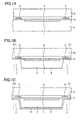
- Figs. 1A to 2C are cross-sectional views for explaining a semiconductor device and its manufacturing method of the invention.
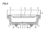
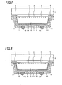
- Figs. 3 to 5, 7 and 8 are cross-sectional views for explaining the semiconductor device of the invention.
- Figs. 6A and 6B are cross-sectional views for explaining a conventional semiconductor device.
- A first embodiment of the invention will be described referring to figures. Figs. 1A to 2C show cross-sectional views of semiconductor device intermediates at corresponding process steps.
- First, as shown in Fig. 1A, a
semiconductor substrate 2 made of silicon (Si) or the like is prepared, where a light receiving element 1 (e.g. an element such as a CCD sensor, a CMOS sensor, or an illumination sensor) that detects an infrared ray having a wavelength of about 700nm to 2500nm is formed on its front surface. Then, a first insulation film 3 (e.g. a silicon oxide film formed by a thermal oxidation method, a CVD method or the like) is formed on the front surface of thesemiconductor substrate 2 to have a thickness of, for example, 2µm. - Then, a metal layer of aluminum (Al), copper (Cu), or the like is formed by a sputtering method, a plating method, or the other deposition method, and the metal layer is etched using a photoresist layer (not shown) as a mask to form a
pad electrode 4 having a thickness of, for example, 1µm on thefirst insulation film 3. Thepad electrode 4 is an external connection electrode electrically connected to thelight receiving element 1 or the surrounding elements. Then, a passivation film (e.g. a silicon nitride film formed by a CVD method) (not shown) is formed on the front surface of thesemiconductor substrate 2, covering a portion of thepad electrode 4. - Then, a light
transparent substrate 6 is attached on the front surface of thesemiconductor substrate 2 including on thepad electrode 4 with aresin layer 5 made of epoxy resin or the like interposed therebetween. The lighttransparent substrate 6 is made of a transparent or semitransparent material such as glass or quartz and has light transmission characteristics. - Then, back-grinding is performed to the back surface of the
semiconductor substrate 2 to thin thesemiconductor substrate 2 to a thickness of, for example, about 100µm. There can be a case where the grinding process is not needed depending on applications or specifications of an end-product and the initial thickness of the preparedsemiconductor substrate 2. - Then, as shown in Fig. 1B, a portion of the
semiconductor substrate 2 in a position corresponding to thepad electrode 4 is selectively etched from the back surface of thesemiconductor substrate 2 to expose thefirst insulation film 3 including thefirst insulation film 3 on a portion of thepad electrode 4. Hereafter, this exposed portion is called anopening 7. Thisopening 7 has a tapered shape of which the diameter is reducing from the back surface toward the front surface of thesemiconductor substrate 2. It is also possible to form theopening 7 in a straight shape so that the side surface of thesemiconductor substrate 2 is vertical to a main surface of the lighttransparent substrate 6 although not shown in the figure. - Then, a
reflection layer 8 made of a metal material such as, for example, aluminum, gold, silver, or the like is formed on a back surface of thesemiconductor substrate 2 by a CVD method, a sputtering method, or the other deposition method to have a thickness of, for example, about 0.1 to 2µm. It is also possible to form thereflection layer 8 after the back grinding of thesemiconductor substrate 2 and then selectively etch thereflection layer 8 and thesemiconductor substrate 2. - The
reflection layer 8 is a layer having a function of reflecting an infrared ray entering from the lighttransparent substrate 6 toward the back surface of thesemiconductor substrate 2 through thesemiconductor substrate 2 or an infrared ray entering from the back surface of thesemiconductor substrate 2 toward thelight receiving element 1 without further transmitting it therethrough, and its material is not particularly limited as long as it has such a function. It is also possible to form thereflection layer 8 uniformly on the whole back surface of thesemiconductor substrate 2 or only under thelight receiving element 1 as described below. - Next, as shown in Fig. 1C, a
second insulation film 9 is formed on the side surface and back surface of thesemiconductor substrate 2 including in theopening 7 and on thereflection layer 8. This second insulation film is a silicon oxide film or a silicon nitride film formed by, for example, a plasma CVD method. - Then, as shown in Fig. 2A, the
first insulation film 3 and thesecond insulation film 9 are selectively etched using a photoresist layer (not shown) as a mask. By this etching, thefirst insulation film 3 and thesecond insulation film 9 formed in a region from on a portion of thepad electrode 4 to a dicing line DL are removed to expose the portion of thepad electrode 4 at a bottom of theopening 7. - Next, a metal layer made of aluminum (Al), copper (Cu) or the like that is to be the
wiring layer 10 is formed by a sputtering method, a plating method, or the other deposition method. Then, as shown in Fig. 2B, this is etched using a photoresist layer (not shown) as a mask to form thewiring layer 10 having a thickness of, for example, 1µm on the portion of thepad electrode 4 and thesecond insulation film 9. It is preferable to form thereflection layer 8 and thewiring layer 10 with the same material (e.g. aluminum) by the same method (e.g. a sputtering method). This is because there are advantages that the manufacturing process is simplified and the manufacturing cost is minimized. - Next, the
protection layer 11 made of a resist material such as a solder resist is formed on the back surface of thesemiconductor substrate 2 including on thewiring layer 10 as shown in Fig. 2C. Then, an opening is formed in a predetermined region of theprotection layer 11, an electrode connection layer (not shown) made of, for example, nickel, gold or the like is formed on thewiring layer 10 exposed in the opening, and the ball-shaped conductive terminal 12 made of solder or the like is formed thereon. When theprotection layer 11 is made of a negative resist material, theprotection layer 11 in a region irradiated with light is left as it is, and theprotection layer 11 in a region irradiated with no light is removed to form the opening. - Wiring from the
pad electrode 4 on the front surface of thesemiconductor substrate 2 to theconductive terminal 12 formed on the back surface of thesemiconductor substrate 2 along the sidewall of thesemiconductor substrate 2 is thus realized in this manner. Then, dicing is performed along the dicing line DL that is a boundary of a number of semiconductor devices into individual separated semiconductor devices. - By the above described processes, the chip size package type semiconductor device having the
light receiving element 1 is completed. - In the semiconductor device of the first embodiment, the
reflection layer 8 is formed between thelight receiving element 1 and thewiring layer 10 in a vertical direction, thereflection layer 8 reflecting an infrared ray toward thelight receiving element 1 without transmitting it to thewiring layer 10, the infrared ray entering from the lighttransparent substrate 6 toward thewiring layer 10 through thesemiconductor substrate 2. Therefore, an infrared ray entering from the lighttransparent substrate 6 and reaching thereflection layer 8 is all reflected by thereflection layer 8. Therefore, since the infrared ray is not reflected by thewiring layer 10 or theconductive terminal 12, any wiring pattern formed on the back surface of thesemiconductor substrate 2 is prevented from being reflected on an output image. Furthermore, an infrared ray entering from the lighttransparent substrate 6 and reaching thereflection layer 8 is reflected toward thelight receiving element 1, thereby providing an advantage that light strength of an infrared ray entering thelight receiving element 1 increases to enhance the contrast of the output image. - Furthermore, although the
reflection layer 8 is uniformly formed on the back surface of thesemiconductor substrate 2 in the above embodiment, it is also possible to form thereflection layer 8 on the back surface of thesemiconductor substrate 2 only in a region overlapping thelight receiving element 1 in the vertical direction or in a larger size than thelight receiving element 1 over an end portion thereof by a predetermined amount, as shown in Fig. 3. This structure also prevents the pattern of thewiring layer 10 from being reflected toward thelight receiving element 1 and prevents the pattern of the wiring on the back surface from being reflected on an output image, in the similar manner to the above embodiment. - Although the
reflection layer 8 is formed only on the back surface of thesemiconductor substrate 2 in the above embodiment, it is also possible to form thereflection layer 8 so as to cover the whole side surface of thesemiconductor substrate 2 as shown in Fig. 7. This structure prevents an infrared ray passing through the lighttransparent substrate 6 from being reflected by thewiring layer 10 formed along the side surface of thesemiconductor substrate 2 toward thelight receiving element 1. Therefore, the pattern of thewiring layer 10 formed along the side surface of thesemiconductor substrate 2 is prevented from being reflected on an output image. - Furthermore, there can be a case where an infrared ray enters from various directions depending on a way of packaging the completed semiconductor device, so that the
light receiving element 1 may mistakenly detect the infrared ray when the infrared ray enters thelight receiving element 1 from the side surface of thesemiconductor substrate 2. On the other hand, by covering the side surface and back surface of thesemiconductor substrate 2 entirely with thereflection layer 8 as shown in Fig. 7, an infrared ray entering from the side surface and back surface of thesemiconductor substrate 2 toward thelight receiving element 1 is completely blocked. Therefore, thelight receiving element 1 accurately receives only light from the lighttransparent substrate 6, thereby enhancing the detection accuracy of thelight receiving element 1. - Furthermore, although the
wiring layer 10 is formed from thepad electrode 4 along the side surface of thesemiconductor substrate 2 in the above embodiment, the embodiment is applicable to any device as long as the wiring layer is formed on the back surface of thesemiconductor substrate 2 therein. That is, for example, in a so-called penetrating electrode type semiconductor device formed with a penetratingelectrode 20 made of metal such as aluminum or copper from the front surface to the back surface of thesemiconductor substrate 2 and awiring layer 21 and a ball-shaped conductive terminal 12 electrically connected to the penetratingelectrode 20 on the back surface of thesemiconductor substrate 2, it is also possible to form thereflection layer 8 between thewiring layer 21 and thelight receiving element 1 including on theconductive terminal 12, as shown in Fig. 4. It is noted that a numeral 22 in Fig. 4 designates a barrier metal layer made of metal such as a titanium (Ti) layer, a titanium oxide (TiO2) layer, a titanium nitride (TiN) layer, a tantalum nitride (TaN) layer or the like, for example. The same numerals are given to the same components as those of the above embodiment, and the description thereof will be omitted. - This penetrating electrode type semiconductor device is formed by, for example, preparing the
semiconductor substrate 2 formed with thepad electrode 4 with thelight receiving element 1 and thefirst insulation film 3 interposed therebetween, forming a via hole penetrating thesemiconductor substrate 2 in a position corresponding to thepad electrode 4, forming thereflection layer 8 on the back surface of thesemiconductor substrate 2, forming asecond insulation film 9a covering a sidewall of the via hole and the back surface of thesemiconductor substrate 2, removing thesecond insulation film 9a on a bottom of the via hole, forming thebarrier metal layer 22 in the via hole, forming the penetratingelectrode 20 made of metal such as copper in the via hole by, for example, an electrolytic plating method, forming thewiring layer 21 electrically connected to the penetratingelectrode 20 on the back surface of thesemiconductor substrate 2 by patterning, and forming the ball-shapedconductive terminal 12 and theprotection layer 11. It is noted that the above described processes are an example of the method of manufacturing the penetrating electrode type semiconductor device of this embodiment, and the invention is not limited to these processes and thereflection layer 8 may be formed before forming the via hole, for example. It is possible to form thereflection layer 8 uniformly on the whole back surface of thesemiconductor substrate 2 or only in a region overlapping thelight receiving element 1 as already described above, although not shown. - Next, a semiconductor device of a second embodiment of the invention will be described referring to Fig. 5. It is noted that the same numerals are given to the same components as those of the first embodiment, and the description thereof will be omitted.
- A feature of the semiconductor device of the second embodiment is that an anti-reflection layer 30 (e.g. a titanium nitride (TiN) layer formed by a sputtering method, a layer added with a pigment such as a black pigment, or an organic resin layer) is formed between the
light receiving element 1 and thewiring layer 10 in a vertical direction to have a thickness of, for example, 1 to 2µm. It is preferable that an infrared ray absorbent material such as, for example, a black pigment is mixed in theanti-reflection layer 30 for enhancing an anti-reflection effect. Theanti-reflection layer 30 absorbs an infrared ray entering from the lighttransparent substrate 6 toward thewiring layer 10 through thesemiconductor substrate 2, and has a function of preventing light transmission. The material and thickness of the anti-reflection layer are not particularly limited as long as it has this function. - In the semiconductor device of the second embodiment, an infrared ray entering from the light
transparent substrate 6 and reaching theanti-reflection layer 30 is absorbed by theanti-reflection layer 30. This effectively prevents an infrared ray from being reflected toward thelight receiving element 1 by thewiring layer 10. Even when an infrared ray is reflected, the amount is very small, thereby minimizing the reflection of the back surface wiring pattern on an output image. - Therefore, any pattern of the
wiring layer 10 or theconductive terminal 12 formed on the back surface of thesemiconductor substrate 2 is effectively prevented from being reflected on an output image. - Furthermore, although the
anti-reflection layer 30 is uniformly formed on the back surface of thesemiconductor substrate 2 in Fig. 5, it is also possible to form theanti-reflection layer 30 on the back surface of thesemiconductor substrate 2 only in a region overlapping thelight receiving element 1 in a vertical direction or in a larger size than thelight receiving element 1 over an end portion thereof by a predetermined amount, in the similar manner to thereflection layer 8 of the semiconductor device shown in Fig. 3. - Furthermore, it is also possible to form the
anti-reflection layer 30 covering the whole side surface of thesemiconductor substrate 2, as shown in Fig. 8. This structure prevents an infrared ray passing through the lighttransparent substrate 6 from being reflected toward thelight receiving element 1 by thewiring layer 10 formed along the side surface of thesemiconductor substrate 2. This prevents the pattern of thewiring layer 10 formed along the side surface of thesemiconductor substrate 2 from being reflected on an output image. - Furthermore, an infrared ray entering from the side surface of the
semiconductor substrate 2 toward thelight receiving element 1 is also absorbed by theanti-reflection layer 30, preventing light transmission. Therefore, in any packaging manner of the semiconductor device, thelight receiving element 1 accurately receives only light entering from the lighttransparent substrate 6, thereby enhancing the detection accuracy of thelight receiving element 1. - The second embodiment of the invention achieves wide application to semiconductor devices as long as those have the wiring layer formed on the back surface of the
semiconductor substrate 2, and this is the same as the first embodiment. Therefore, this may be applied to the so-called penetrating electrode type semiconductor device shown in Fig. 4. - Although the description of the above embodiments is given for the BGA type semiconductor device having the ball-shaped conductive terminal, the invention may be applied to the LGA (land grid array) type semiconductor device.
The embodiments achieve prevention of reflection of the patterns of the conductive terminal and the wiring layer formed on the back surface of the semiconductor substrate on an output image.
Claims (8)
- A semiconductor device comprising:a semiconductor substrate (2) comprising a front surface and a back surfacea light receiving element (1) formed on the front surface of the semiconductor substrate (2);a transparent substrate (6) attached to the front surface of the semiconductor substrate (2) so as to cover the light receiving element (1);a wiring layer (9) formed on the back surface of the semiconductor substrate (2); anda reflection layer (8) formed on the back surface of the semiconductor substrate (2) and located between the light receiving element (1) and the wiring layer (9), the reflecting layer (8) being configured to reflect an infrared ray passing through the transparent substrate (6), the light receiving element (1) and the semiconductor substrate (2) back toward to the light receiving element (1).
- The semiconductor device of claim 1, wherein the reflection layer (8) is confined to an area of the back surface of the semiconductor substrate (2) that is a projection of the light receiving element (1) onto the back surface.
- The semiconductor device of claim 1 or 2, wherein the wiring layer (9) extends to be on a side surface of the semiconductor substrate (2), and the reflection layer (8) extends to be between the extending wiring layer (9) and the side surface of the semiconductor substrate (2).
- The semiconductor device according to any of claims 1 to 3, wherein the reflection layer (8) comprises a metal.
- A semiconductor device comprising:a semiconductor substrate (2) comprising a front surface and a back surface;a light receiving element (1) formed on the front surface of the semiconductor substrate (2);a transparent substrate (6) attached to the front surface of the semiconductor substrate (2) so as to cover the light receiving element (1);a wiring layer (9) formed on the back surface of the semiconductor substrate (2); andan anti-reflection layer (30) formed on the back surface of the semiconductor substrate (2) and located between the light receiving element (1) and the wiring layer (9), the anti-reflection layer (30) being configured to absorb an infrared ray.
- The semiconductor device of claim 5, wherein the anti-reflection layer (30) is confined to an area of the back surface of the semiconductor substrate (2) that is a projection of the light receiving element (1) onto the back surface.
- The semiconductor device of claim 5 or 6, wherein the wiring layer (9) extends to be on a side surface of the semiconductor substrate (2), and the anti-reflection layer (30) extends to be between the extending wiring layer (9) and the side surface of the semiconductor substrate (2).
- The semiconductor device according to any of claims 5 to 7, wherein the anti-reflection layer (30) comprises an infrared ray absorbent material mixed therein.
Applications Claiming Priority (2)
| Application Number | Priority Date | Filing Date | Title |
|---|---|---|---|
| JP2005361706 | 2005-12-15 | ||
| JP2006310623A JP5010244B2 (en) | 2005-12-15 | 2006-11-16 | Semiconductor device |
Publications (2)
| Publication Number | Publication Date |
|---|---|
| EP1798769A2 true EP1798769A2 (en) | 2007-06-20 |
| EP1798769A3 EP1798769A3 (en) | 2009-07-08 |
Family
ID=37858482
Family Applications (1)
| Application Number | Title | Priority Date | Filing Date |
|---|---|---|---|
| EP20060026088 Withdrawn EP1798769A3 (en) | 2005-12-15 | 2006-12-15 | Semiconductor device |
Country Status (6)
| Country | Link |
|---|---|
| US (1) | US7986021B2 (en) |
| EP (1) | EP1798769A3 (en) |
| JP (1) | JP5010244B2 (en) |
| KR (1) | KR20070064273A (en) |
| SG (1) | SG133537A1 (en) |
| TW (1) | TWI343645B (en) |
Cited By (1)
| Publication number | Priority date | Publication date | Assignee | Title |
|---|---|---|---|---|
| WO2009103048A1 (en) * | 2008-02-14 | 2009-08-20 | Quantum Semiconductor Llc | Dual photo-diode cmos pixels |
Families Citing this family (19)
| Publication number | Priority date | Publication date | Assignee | Title |
|---|---|---|---|---|
| JP2007165696A (en) * | 2005-12-15 | 2007-06-28 | Sanyo Electric Co Ltd | Semiconductor device and manufacturing method thereof |
| JP5301108B2 (en) * | 2007-04-20 | 2013-09-25 | セミコンダクター・コンポーネンツ・インダストリーズ・リミテッド・ライアビリティ・カンパニー | Semiconductor device |
| JP2009032929A (en) * | 2007-07-27 | 2009-02-12 | Sanyo Electric Co Ltd | Semiconductor device and manufacturing method thereof |
| TWI382477B (en) * | 2007-08-24 | 2013-01-11 | 精材科技股份有限公司 | Wafer level package of electronic component and manufacturing method thereof |
| TWI375321B (en) * | 2007-08-24 | 2012-10-21 | Xintec Inc | Electronic device wafer level scale packages and fabrication methods thereof |
| JP2009099591A (en) | 2007-10-12 | 2009-05-07 | Toshiba Corp | Solid-state imaging device and manufacturing method thereof |
| KR101446330B1 (en) * | 2008-01-29 | 2014-10-02 | 삼성전자주식회사 | Image sensor with through vias |
| JP2010103300A (en) * | 2008-10-23 | 2010-05-06 | Sanyo Electric Co Ltd | Semiconductor device, and method of manufacturing the same |
| US8298917B2 (en) * | 2009-04-14 | 2012-10-30 | International Business Machines Corporation | Process for wet singulation using a dicing singulation structure |
| WO2011058977A1 (en) * | 2009-11-10 | 2011-05-19 | ローム株式会社 | Semiconductor device and method for manufacturing semiconductor device |
| CN101789414B (en) * | 2010-02-26 | 2011-08-17 | 苏州晶方半导体科技股份有限公司 | Ultrathin semiconductor chip packaging structure and manufacturing process thereof |
| KR101731047B1 (en) * | 2010-12-01 | 2017-05-12 | 삼성디스플레이 주식회사 | Ir sensing transistor and manufacturing method of display device including thesame |
| US9711403B2 (en) * | 2011-01-17 | 2017-07-18 | Xintec Inc. | Method for forming chip package |
| JP6215612B2 (en) * | 2013-08-07 | 2017-10-18 | ソニーセミコンダクタソリューションズ株式会社 | LIGHT EMITTING ELEMENT, LIGHT EMITTING ELEMENT WAFER, AND ELECTRONIC DEVICE |
| TWI569427B (en) * | 2014-10-22 | 2017-02-01 | 精材科技股份有限公司 | Semiconductor package and its manufacturing method |
| US20180376041A1 (en) * | 2015-12-24 | 2018-12-27 | Kyocera Corporation | Image sensor mounting board and imaging device |
| JP2018133392A (en) * | 2017-02-14 | 2018-08-23 | キヤノン株式会社 | Photoelectric conversion device |
| JP7204667B2 (en) * | 2017-04-20 | 2023-01-16 | トリナミクス ゲゼルシャフト ミット ベシュレンクテル ハフツング | photodetector |
| US11976979B2 (en) | 2019-01-29 | 2024-05-07 | Trinamix Gmbh | Optical detector |
Family Cites Families (65)
| Publication number | Priority date | Publication date | Assignee | Title |
|---|---|---|---|---|
| JPS6057714B2 (en) * | 1978-01-27 | 1985-12-16 | 株式会社日立製作所 | Optical semiconductor device |
| JPH0521698A (en) | 1991-07-11 | 1993-01-29 | Mitsubishi Electric Corp | Semiconductor device |
| JP3242495B2 (en) * | 1993-07-01 | 2001-12-25 | シャープ株式会社 | Photodetector with multilayer filter and method of manufacturing the same |
| JP2674545B2 (en) * | 1995-01-20 | 1997-11-12 | 日本電気株式会社 | Infrared detector and driving method thereof |
| US5804827A (en) * | 1995-10-27 | 1998-09-08 | Nikon Corporation | Infrared ray detection device and solid-state imaging apparatus |
| US6563192B1 (en) | 1995-12-22 | 2003-05-13 | Micron Technology, Inc. | Semiconductor die with integral decoupling capacitor |
| JPH09321333A (en) | 1996-05-24 | 1997-12-12 | Nikon Corp | Infrared detector |
| US5929440A (en) * | 1996-10-25 | 1999-07-27 | Hypres, Inc. | Electromagnetic radiation detector |
| US5981314A (en) * | 1996-10-31 | 1999-11-09 | Amkor Technology, Inc. | Near chip size integrated circuit package |
| US5982018A (en) | 1997-05-23 | 1999-11-09 | Micron Technology, Inc. | Thin film capacitor coupons for memory modules and multi-chip modules |
| US5973337A (en) * | 1997-08-25 | 1999-10-26 | Motorola, Inc. | Ball grid device with optically transmissive coating |
| JPH11167154A (en) * | 1997-12-03 | 1999-06-22 | Olympus Optical Co Ltd | Flexible printed circuit board |
| IL123207A0 (en) * | 1998-02-06 | 1998-09-24 | Shellcase Ltd | Integrated circuit device |
| JP3601761B2 (en) * | 1998-11-19 | 2004-12-15 | 松下電器産業株式会社 | Light receiving element and method of manufacturing the same |
| US6236103B1 (en) | 1999-03-31 | 2001-05-22 | International Business Machines Corp. | Integrated high-performance decoupling capacitor and heat sink |
| JP2000349238A (en) | 1999-06-04 | 2000-12-15 | Seiko Epson Corp | Semiconductor device |
| US6326689B1 (en) * | 1999-07-26 | 2001-12-04 | Stmicroelectronics, Inc. | Backside contact for touchchip |
| US6465786B1 (en) * | 1999-09-01 | 2002-10-15 | Micron Technology, Inc. | Deep infrared photodiode for a CMOS imager |
| JP2001128072A (en) * | 1999-10-29 | 2001-05-11 | Sony Corp | Imaging device, imaging device, camera module, and camera system |
| JP2001085652A (en) * | 1999-09-09 | 2001-03-30 | Sony Corp | Infrared CCD image sensor package |
| JP3632558B2 (en) * | 1999-09-17 | 2005-03-23 | 日立化成工業株式会社 | Epoxy resin composition for sealing and electronic component device |
| JP3514681B2 (en) * | 1999-11-30 | 2004-03-31 | 三菱電機株式会社 | Infrared detector |
| US6455774B1 (en) | 1999-12-08 | 2002-09-24 | Amkor Technology, Inc. | Molded image sensor package |
| JP2002094082A (en) | 2000-07-11 | 2002-03-29 | Seiko Epson Corp | Optical element, method of manufacturing the same, and electronic device |
| JP2002033473A (en) * | 2000-07-17 | 2002-01-31 | Hamamatsu Photonics Kk | Semiconductor device |
| JP3409848B2 (en) | 2000-08-29 | 2003-05-26 | 日本電気株式会社 | Thermal infrared detector |
| US7141803B2 (en) * | 2000-09-11 | 2006-11-28 | Hamamatsu Photonics K.K. | Scintillator panel, radiation image sensor and methods of producing them |
| KR20020048716A (en) | 2000-12-18 | 2002-06-24 | 박종섭 | Image sensor having reflection layer on back side of semiconductor substrate and method for fabricating the same |
| JP3910817B2 (en) | 2000-12-19 | 2007-04-25 | ユーディナデバイス株式会社 | Semiconductor photo detector |
| JP2002329850A (en) * | 2001-05-01 | 2002-11-15 | Canon Inc | Chip size package and manufacturing method thereof |
| DE10142481A1 (en) * | 2001-08-31 | 2003-03-27 | Rudolf Hezel | Solar cell and method for producing such |
| TWI232560B (en) | 2002-04-23 | 2005-05-11 | Sanyo Electric Co | Semiconductor device and its manufacture |
| JP2003347476A (en) * | 2002-05-22 | 2003-12-05 | Sanyo Electric Co Ltd | Semiconductor integrated device and method of manufacturing the same |
| JP3923368B2 (en) | 2002-05-22 | 2007-05-30 | シャープ株式会社 | Manufacturing method of semiconductor device |
| JP4037197B2 (en) * | 2002-07-17 | 2008-01-23 | 富士フイルム株式会社 | Manufacturing method of semiconductor imaging device mounting structure |
| US20040108588A1 (en) * | 2002-09-24 | 2004-06-10 | Cookson Electronics, Inc. | Package for microchips |
| US7033664B2 (en) * | 2002-10-22 | 2006-04-25 | Tessera Technologies Hungary Kft | Methods for producing packaged integrated circuit devices and packaged integrated circuit devices produced thereby |
| TWI239607B (en) | 2002-12-13 | 2005-09-11 | Sanyo Electric Co | Method for making a semiconductor device |
| JP5030360B2 (en) | 2002-12-25 | 2012-09-19 | オリンパス株式会社 | Method for manufacturing solid-state imaging device |
| JP2004260135A (en) | 2003-02-06 | 2004-09-16 | Sanyo Electric Co Ltd | Semiconductor integrated device and method of manufacturing the same |
| JP2004319530A (en) | 2003-02-28 | 2004-11-11 | Sanyo Electric Co Ltd | Optical semiconductor device and method of manufacturing the same |
| JP2004311783A (en) * | 2003-04-08 | 2004-11-04 | Fuji Xerox Co Ltd | Photodetector and its mounting method |
| TWI229890B (en) | 2003-04-24 | 2005-03-21 | Sanyo Electric Co | Semiconductor device and method of manufacturing same |
| WO2005004195A2 (en) | 2003-07-03 | 2005-01-13 | Shellcase Ltd. | Method and apparatus for packaging integrated circuit devices |
| JP4401181B2 (en) | 2003-08-06 | 2010-01-20 | 三洋電機株式会社 | Semiconductor device and manufacturing method thereof |
| US7329861B2 (en) | 2003-10-14 | 2008-02-12 | Micron Technology, Inc. | Integrally packaged imaging module |
| JP2005327984A (en) * | 2004-05-17 | 2005-11-24 | Shinko Electric Ind Co Ltd | Electronic component and method for manufacturing electronic component mounting structure |
| US7332408B2 (en) | 2004-06-28 | 2008-02-19 | Micron Technology, Inc. | Isolation trenches for memory devices |
| JP4271625B2 (en) | 2004-06-30 | 2009-06-03 | 株式会社フジクラ | Semiconductor package and manufacturing method thereof |
| JP2006093367A (en) | 2004-09-24 | 2006-04-06 | Sanyo Electric Co Ltd | Manufacturing method of semiconductor device |
| TWI273682B (en) | 2004-10-08 | 2007-02-11 | Epworks Co Ltd | Method for manufacturing wafer level chip scale package using redistribution substrate |
| US7374971B2 (en) | 2005-04-20 | 2008-05-20 | Freescale Semiconductor, Inc. | Semiconductor die edge reconditioning |
| KR100629498B1 (en) | 2005-07-15 | 2006-09-28 | 삼성전자주식회사 | Micro-Packages, Multi-Stack Micro-Packages, and Methods for Making the Same |
| US7576361B2 (en) * | 2005-08-03 | 2009-08-18 | Aptina Imaging Corporation | Backside silicon wafer design reducing image artifacts from infrared radiation |
| JP2007165696A (en) | 2005-12-15 | 2007-06-28 | Sanyo Electric Co Ltd | Semiconductor device and manufacturing method thereof |
| JP2007184680A (en) * | 2006-01-04 | 2007-07-19 | Fujifilm Corp | Solid-state imaging device and manufacturing method thereof |
| TW200737506A (en) | 2006-03-07 | 2007-10-01 | Sanyo Electric Co | Semiconductor device and manufacturing method of the same |
| US8102039B2 (en) | 2006-08-11 | 2012-01-24 | Sanyo Semiconductor Co., Ltd. | Semiconductor device and manufacturing method thereof |
| US7569409B2 (en) | 2007-01-04 | 2009-08-04 | Visera Technologies Company Limited | Isolation structures for CMOS image sensor chip scale packages |
| WO2008093880A1 (en) | 2007-02-02 | 2008-08-07 | Sanyo Electric Co., Ltd. | Semiconductor device and method for manufacturing the same |
| JP5301108B2 (en) | 2007-04-20 | 2013-09-25 | セミコンダクター・コンポーネンツ・インダストリーズ・リミテッド・ライアビリティ・カンパニー | Semiconductor device |
| JP2008294405A (en) | 2007-04-25 | 2008-12-04 | Sanyo Electric Co Ltd | Semiconductor device and manufacturing method thereof |
| TW200845339A (en) | 2007-05-07 | 2008-11-16 | Sanyo Electric Co | Semiconductor device and manufacturing method thereof |
| JP2009032929A (en) | 2007-07-27 | 2009-02-12 | Sanyo Electric Co Ltd | Semiconductor device and manufacturing method thereof |
| CN101123231B (en) | 2007-08-31 | 2010-11-03 | 晶方半导体科技(苏州)有限公司 | Micro-electromechanical system wafer-level chip-scale packaging structure and manufacturing method thereof |
-
2006
- 2006-11-16 JP JP2006310623A patent/JP5010244B2/en active Active
- 2006-12-06 TW TW95145296A patent/TWI343645B/en not_active IP Right Cessation
- 2006-12-14 KR KR20060127760A patent/KR20070064273A/en not_active Ceased
- 2006-12-15 EP EP20060026088 patent/EP1798769A3/en not_active Withdrawn
- 2006-12-15 SG SG200608735-7A patent/SG133537A1/en unknown
- 2006-12-15 US US11/639,410 patent/US7986021B2/en active Active
Cited By (1)
| Publication number | Priority date | Publication date | Assignee | Title |
|---|---|---|---|---|
| WO2009103048A1 (en) * | 2008-02-14 | 2009-08-20 | Quantum Semiconductor Llc | Dual photo-diode cmos pixels |
Also Published As
| Publication number | Publication date |
|---|---|
| SG133537A1 (en) | 2007-07-30 |
| KR20070064273A (en) | 2007-06-20 |
| US20070145420A1 (en) | 2007-06-28 |
| EP1798769A3 (en) | 2009-07-08 |
| TWI343645B (en) | 2011-06-11 |
| US7986021B2 (en) | 2011-07-26 |
| TW200731520A (en) | 2007-08-16 |
| JP2007189198A (en) | 2007-07-26 |
| JP5010244B2 (en) | 2012-08-29 |
Similar Documents
| Publication | Publication Date | Title |
|---|---|---|
| US7986021B2 (en) | Semiconductor device | |
| US8174090B2 (en) | Packaging structure | |
| US7633133B2 (en) | Semiconductor device and manufacturing method of the same | |
| US7944015B2 (en) | Semiconductor device and method of manufacturing the same | |
| US7589388B2 (en) | Semiconductor device and method of manufacturing the same | |
| CN100587962C (en) | Method and apparatus for packaging integrated circuit devices | |
| KR102103393B1 (en) | Image sensing chip packaging structure and packaging method | |
| US7576402B2 (en) | Semiconductor device, method of manufacturing the same, and camera module | |
| US7397134B2 (en) | Semiconductor device mounted on and electrically connected to circuit board | |
| US8053852B2 (en) | Light sensor receiving light from backside | |
| CN100502022C (en) | Semiconductor device | |
| CN100546038C (en) | Semiconductor device and manufacturing method thereof | |
| US20180301488A1 (en) | Image sensing chip packaging structure and packaging method | |
| EP1879230A1 (en) | Semiconductor device and manufacturing method of the same | |
| KR20080004183A (en) | Semiconductor device and manufacturing method thereof |
Legal Events
| Date | Code | Title | Description |
|---|---|---|---|
| PUAI | Public reference made under article 153(3) epc to a published international application that has entered the european phase |
Free format text: ORIGINAL CODE: 0009012 |
|
| AK | Designated contracting states |
Kind code of ref document: A2 Designated state(s): AT BE BG CH CY CZ DE DK EE ES FI FR GB GR HU IE IS IT LI LT LU LV MC NL PL PT RO SE SI SK TR |
|
| AX | Request for extension of the european patent |
Extension state: AL BA HR MK YU |
|
| PUAL | Search report despatched |
Free format text: ORIGINAL CODE: 0009013 |
|
| AK | Designated contracting states |
Kind code of ref document: A3 Designated state(s): AT BE BG CH CY CZ DE DK EE ES FI FR GB GR HU IE IS IT LI LT LU LV MC NL PL PT RO SE SI SK TR |
|
| AX | Request for extension of the european patent |
Extension state: AL BA HR MK RS |
|
| AKX | Designation fees paid | ||
| STAA | Information on the status of an ep patent application or granted ep patent |
Free format text: STATUS: THE APPLICATION IS DEEMED TO BE WITHDRAWN |
|
| 18D | Application deemed to be withdrawn |
Effective date: 20100109 |
|
| REG | Reference to a national code |
Ref country code: DE Ref legal event code: 8566 |