EP1798562A1 - Qualified anomaly detection - Google Patents
Qualified anomaly detection Download PDFInfo
- Publication number
- EP1798562A1 EP1798562A1 EP06256199A EP06256199A EP1798562A1 EP 1798562 A1 EP1798562 A1 EP 1798562A1 EP 06256199 A EP06256199 A EP 06256199A EP 06256199 A EP06256199 A EP 06256199A EP 1798562 A1 EP1798562 A1 EP 1798562A1
- Authority
- EP
- European Patent Office
- Prior art keywords
- trigger
- serial data
- data stream
- recited
- circuit
- Prior art date
- Legal status (The legal status is an assumption and is not a legal conclusion. Google has not performed a legal analysis and makes no representation as to the accuracy of the status listed.)
- Granted
Links
Images

Classifications
-
- G—PHYSICS
- G01—MEASURING; TESTING
- G01R—MEASURING ELECTRIC VARIABLES; MEASURING MAGNETIC VARIABLES
- G01R13/00—Arrangements for displaying electric variables or waveforms
- G01R13/02—Arrangements for displaying electric variables or waveforms for displaying measured electric variables in digital form
- G01R13/0218—Circuits therefor
- G01R13/0254—Circuits therefor for triggering, synchronisation
Definitions
- the present invention relates to analysis of digital data, and more particularly to a method of qualified anomaly detection in order to detect and trigger on specific analog anomalies and/or digital data within a qualified area of a serial data stream.
- Oscilloscope trigger circuits have become exceedingly complex, enabling a user to trigger on almost any type of analog anomaly within an input electrical signal in order to acquire data for the analysis of the particular anomaly. Some trigger circuits also allow the user to trigger on a particular data word or event within a serial digital data stream.
- serial data streams encompass many levels of hierarchy, as exemplified by the OSI (Open System Interconnection) model that defines a networking framework for implementing protocols in seven layers. These serial data streams have framed data accompanied by several higher layer protocols that are used to route/identify the data. This makes debugging of a physical event or anomaly within a specific portion of the serial data stream difficult. Since these serial data streams tend to be quite noisy, analog anomalies may be particularly problematic when the serial data streams are decoded for information content. Such anomalies may result in misinterpretation of the bits within the serial data stream.
- Logic analyzers have the capability to trigger on anomalies if they have digital characteristics and thresholds only, but do not have the ability to trigger on analog anomalies representative of signal fidelity.
- What is desired is a method of detecting and triggering on specific analog anomalies and/or digital data within a qualified area of the serial data stream.
- the present invention provides a method of qualified anomaly detection that provides detection and triggering on specific analog anomalies and/or digital data within a qualified area of a serial data stream.
- a start pattern within the serial data stream such as a packet header for a packetized data stream or other identifiable event, is detected to generate an enable signal.
- a stop event such as a packet trailer, a specified digital event, a time interval or the like, is identified to generate a disable signal.
- the enable and disable signals are combined to produce a qualification signal that allows a trigger circuit to trigger on a specified anomaly within the portion of the serial data stream defined by the qualification signal.
- Fig. 1 is an event timing diagram view illustrating qualified anomaly detection according to the present invention.
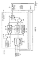
- Fig. 2 is a block diagram view of an apparatus for qualified anomaly detection according to the present invention.
- a serial data stream such as a SONET data stream, is shown having a plurality of data packets in a sequence. As indicated some of the data packets have signal anomalies present within them. The user is only interested in certain data packets or portions of the serial data stream, and so is interested in capturing data surrounding an anomaly within any of the data packets or portions of interest. The remainder of Fig. 1 shows the timing within the data packet of interest indicated as having an anomaly. The process described below applies to each of the data packets or portions of interest, but only the anomalous data packet or portion of interest produces a trigger signal.
- the serial data is a series of alternating signal levels corresponding to logic levels, such as "0" or "1."
- a group of "bits" that have a unique pattern indicating the beginning of a particular portion of the serial data of interest, i.e., a header may be used for packetized data as in this example.
- a group of "bits” that have a unique pattern indicating the end of the particular portion of the serial data of interest, i.e., a trailer may be used for packetized data as in this example.
- the user is looking for any anomalies that might cause an error when the serial data is decoded.
- a (c) clock recovered from the serial data, or an external clock that is comparable to the recovered clock, is used for timing.
- a qualification start signal is generated and at the end of the trailer or stop event (e) a qualification stop signal is generated.
- the interval between the qualification start and stop produces (f) an arm signal that enables a trigger circuit in order to acquire data within the armed interval that represents a specified anomaly.
- the trigger circuit When the specified anomaly occurs, such as a runt, glitch, spike, serial pattern, etc., the trigger circuit generates (g) a trigger signal that causes data surrounding the specified anomaly to be captured for analysis, as is well known in the art.
- a qualification circuit 10 receives the serial data streams from the input channels at a cross-point switch 12 which routes one of the input channels to an output.
- the cross-point switch 12 also provides the ability to convert a multi-lane data stream across multiple inputs into a single serial data stream at the output.
- the selected serial digital stream from the cross-point switch 12 is input to a clock recovery circuit 14, a start word recognizer 16, a stop word recognizer 18 and a timer/event recognizer 20.
- the embedded clock in the serial data stream is recovered by the clock recovery circuit 14 and used to provide timing for the various recognizers 16, 18, 20.
- an external clock that is equivalent to the embedded clock may be selected in lieu of the recovered clock by a clock multiplexer 22 for use as the timing source.
- the respective word recognizers 16, 18 look at respective unique data patterns indicating a starting point in the selected serial data stream and a stopping point in the selected serial data stream that define the portion of the serial data stream of interest. The data stream is clocked into each of the word recognizers 16, 18 by the recovered clock.
- the output from the start word recognizer 16 is input to an arm/disarm circuit 24 to cause the output from the arm/disarm circuit to provide an enable signal to the main trigger circuit 30, at which point the main trigger circuit starts looking for the specified anomaly in the channel input(s).
- the output from the stop word recognizer 18 also is input to the arm/disarm circuit 24 to cause the output from the arm/disarm circuit to provide a disable signal to the main trigger circuit 30, at which point the main trigger circuit stops looking for the specified anomaly in the channel input(s).
- the output from the start word recognizer 16 may be used to enable the timer/event recognizer 20 to provide the disable signal via a stop multiplexer 26 to the arm/disarm circuit 24.
- the timer/event recognizer 20 is reset or initiated by the output from the start word recognizer 16 and counts the recovered clock pulses until a specified time period ends, at which point the timer/event recognizer outputs the disable signal.
- the timer may be either an up-counter or a down-counter.
- As an event recognizer the timer/event recognizer 20 looks for a specified pattern in the selected serial data stream as a terminal event that generates the disable signal.
- the stop multiplexer 26 may also be implemented using OR logic so that if either the trailer or specified event occurs, the disable signal is generated for the arm/disarm circuit 24.
- a packet header for the selected serial data stream is programmed as the trigger enable signal while a packet trailer is programmed as the trigger disable signal. If the runt or glitch occurs in the packet between the header and trailer, the trigger circuit generates a trigger to capture the surrounding data for analysis.
- the described invention is unrelated to any particular standard.
- some standards may have a particular pattern that repeats multiple times, but only after a certain number of iterations is actual information data transmitted. In this case the number of iterations of the identified pattern is counted as part of the start pattern that determines when the trigger circuit is qualified to start looking for analog anomalies in the serial data stream.
- Other standards may have periodic dead times, which dead times could be identified and a time after the end of the dead time specified as the start event for qualifying the trigger circuit. Therefore any identifiable pattern or sequence of patterns in the serial data stream may be identified as the start event depending on the particular data standard used for the serial data stream.
- the present invention simplifies the triggering in a serial data stream by recognizing a specified start pattern before enabling a physical trigger circuit, and then recognizing a specified stop pattern, event or time period to disable the trigger circuit.
Landscapes
- Physics & Mathematics (AREA)
- General Physics & Mathematics (AREA)
- Data Exchanges In Wide-Area Networks (AREA)
- Information Transfer Systems (AREA)
- Communication Control (AREA)
- Maintenance And Management Of Digital Transmission (AREA)
Abstract
Description
- The present invention relates to analysis of digital data, and more particularly to a method of qualified anomaly detection in order to detect and trigger on specific analog anomalies and/or digital data within a qualified area of a serial data stream.
- Oscilloscope trigger circuits have become exceedingly complex, enabling a user to trigger on almost any type of analog anomaly within an input electrical signal in order to acquire data for the analysis of the particular anomaly. Some trigger circuits also allow the user to trigger on a particular data word or event within a serial digital data stream. However serial data streams encompass many levels of hierarchy, as exemplified by the OSI (Open System Interconnection) model that defines a networking framework for implementing protocols in seven layers. These serial data streams have framed data accompanied by several higher layer protocols that are used to route/identify the data. This makes debugging of a physical event or anomaly within a specific portion of the serial data stream difficult. Since these serial data streams tend to be quite noisy, analog anomalies may be particularly problematic when the serial data streams are decoded for information content. Such anomalies may result in misinterpretation of the bits within the serial data stream.
- Logic analyzers have the capability to trigger on anomalies if they have digital characteristics and thresholds only, but do not have the ability to trigger on analog anomalies representative of signal fidelity.
- What is desired is a method of detecting and triggering on specific analog anomalies and/or digital data within a qualified area of the serial data stream.
- Accordingly the present invention provides a method of qualified anomaly detection that provides detection and triggering on specific analog anomalies and/or digital data within a qualified area of a serial data stream. A start pattern within the serial data stream, such as a packet header for a packetized data stream or other identifiable event, is detected to generate an enable signal. A stop event, such as a packet trailer, a specified digital event, a time interval or the like, is identified to generate a disable signal. The enable and disable signals are combined to produce a qualification signal that allows a trigger circuit to trigger on a specified anomaly within the portion of the serial data stream defined by the qualification signal.
- The objects, advantages and other novel features of the present invention are apparent from the following detailed description when read in light of the appended claims and attached drawing.
- Fig. 1 is an event timing diagram view illustrating qualified anomaly detection according to the present invention.
- Fig. 2 is a block diagram view of an apparatus for qualified anomaly detection according to the present invention.
- Referring now to Fig. 1 (a) a serial data stream, such as a SONET data stream, is shown having a plurality of data packets in a sequence. As indicated some of the data packets have signal anomalies present within them. The user is only interested in certain data packets or portions of the serial data stream, and so is interested in capturing data surrounding an anomaly within any of the data packets or portions of interest. The remainder of Fig. 1 shows the timing within the data packet of interest indicated as having an anomaly. The process described below applies to each of the data packets or portions of interest, but only the anomalous data packet or portion of interest produces a trigger signal.
- As shown (b) the serial data is a series of alternating signal levels corresponding to logic levels, such as "0" or "1." Within the serial data is a group of "bits" that have a unique pattern indicating the beginning of a particular portion of the serial data of interest, i.e., a header may be used for packetized data as in this example. Likewise within the serial data is a group of "bits" that have a unique pattern indicating the end of the particular portion of the serial data of interest, i.e., a trailer may be used for packetized data as in this example. Within this portion of the serial data between the header and trailer, or start event and stop event, the user is looking for any anomalies that might cause an error when the serial data is decoded. A (c) clock recovered from the serial data, or an external clock that is comparable to the recovered clock, is used for timing. At the end of the header or start event (d) a qualification start signal is generated and at the end of the trailer or stop event (e) a qualification stop signal is generated. The interval between the qualification start and stop produces (f) an arm signal that enables a trigger circuit in order to acquire data within the armed interval that represents a specified anomaly. When the specified anomaly occurs, such as a runt, glitch, spike, serial pattern, etc., the trigger circuit generates (g) a trigger signal that causes data surrounding the specified anomaly to be captured for analysis, as is well known in the art.
- As shown in Fig. 2 various channel inputs carrying serial data streams, or a multi-lane serial data stream, are input both to a
qualification circuit 10 as described below and to a conventionalmain trigger circuit 30. Thequalification circuit 10 receives the serial data streams from the input channels at across-point switch 12 which routes one of the input channels to an output. Thecross-point switch 12 also provides the ability to convert a multi-lane data stream across multiple inputs into a single serial data stream at the output. The selected serial digital stream from thecross-point switch 12 is input to aclock recovery circuit 14, astart word recognizer 16, a stop word recognizer 18 and a timer/event recognizer 20. The embedded clock in the serial data stream is recovered by theclock recovery circuit 14 and used to provide timing for thevarious recognizers clock multiplexer 22 for use as the timing source. Therespective word recognizers word recognizers start word recognizer 16 is input to an arm/disarm circuit 24 to cause the output from the arm/disarm circuit to provide an enable signal to themain trigger circuit 30, at which point the main trigger circuit starts looking for the specified anomaly in the channel input(s). The output from thestop word recognizer 18 also is input to the arm/disarm circuit 24 to cause the output from the arm/disarm circuit to provide a disable signal to themain trigger circuit 30, at which point the main trigger circuit stops looking for the specified anomaly in the channel input(s). - Alternatively the output from the
start word recognizer 16 may be used to enable the timer/event recognizer 20 to provide the disable signal via astop multiplexer 26 to the arm/disarm circuit 24. As a timer the timer/event recognizer 20 is reset or initiated by the output from the start word recognizer 16 and counts the recovered clock pulses until a specified time period ends, at which point the timer/event recognizer outputs the disable signal. The timer may be either an up-counter or a down-counter. As an event recognizer the timer/event recognizer 20 looks for a specified pattern in the selected serial data stream as a terminal event that generates the disable signal. Thestop multiplexer 26 may also be implemented using OR logic so that if either the trailer or specified event occurs, the disable signal is generated for the arm/disarm circuit 24. - As a specific example if a trigger on a runt or glitch that occurs within a data packet having a specific header is desired, a packet header for the selected serial data stream is programmed as the trigger enable signal while a packet trailer is programmed as the trigger disable signal. If the runt or glitch occurs in the packet between the header and trailer, the trigger circuit generates a trigger to capture the surrounding data for analysis.
- Although the above description relates in detail to a packetized communications standard, the described invention is unrelated to any particular standard. For example, not all standards are packetized. Some standards may have a particular pattern that repeats multiple times, but only after a certain number of iterations is actual information data transmitted. In this case the number of iterations of the identified pattern is counted as part of the start pattern that determines when the trigger circuit is qualified to start looking for analog anomalies in the serial data stream. Other standards may have periodic dead times, which dead times could be identified and a time after the end of the dead time specified as the start event for qualifying the trigger circuit. Therefore any identifiable pattern or sequence of patterns in the serial data stream may be identified as the start event depending on the particular data standard used for the serial data stream.
- Thus the present invention simplifies the triggering in a serial data stream by recognizing a specified start pattern before enabling a physical trigger circuit, and then recognizing a specified stop pattern, event or time period to disable the trigger circuit.
Claims (20)
- A method of qualifying a trigger event comprising the steps of:detecting a start pattern in a serial data stream to provide an enable signal for a trigger circuit; andidentifying a stop event after the start pattern to provide a disable signal for the trigger circuit so that the trigger circuit provides a trigger signal when the trigger event occurs in the serial data stream between the start pattern and the stop event.
- The method as recited in claim 1 wherein the identifying step comprises the step of detecting a stop pattern in the serial data stream as the stop event.
- The method as recited in claim 2 wherein the stop pattern comprises a packet trailer indicating the end of a data packet of interest within the serial data stream.
- The method as recited in claim 1 wherein the identifying step comprises the step of detecting a specified pattern in the serial data stream as the stop event.
- The method as recited in claim 1 wherein the identifying step comprises the step of generating the stop event at a specified time interval after the start pattern.
- The method as recited in any of claims 1-5 wherein the start pattern comprises a packet header indicating the start of a data packet of interest within the serial data stream.
- A trigger qualification circuit comprising:means for detecting a start pattern in a serial data stream to provide an enable signal for a trigger circuit;means for identifying a stop event after the start pattern to provide a disable signal for the trigger circuit so that the trigger circuit is enabled to provide a trigger signal only in the interval between the start pattern and the stop event.
- The trigger qualification circuit as recited in claim 7 further comprising means for selecting the serial data stream from among a plurality of inputs for input to the detecting and identifying means.
- The trigger qualification circuit as recited in claim 8 wherein the selecting means comprises means for generating the serial data stream from the plurality of inputs representing a multi-lane serial data stream.
- The trigger qualification circuit as recited in claim 9 wherein the selecting means comprises a cross-point switch having a plurality of input ports for receiving the plurality of inputs and having an output port for providing the serial data stream to the detecting means.
- The trigger qualification circuit as recited in claim 7 wherein the identifying means comprises means for combining the enable and disable signals to provide a qualification signal to the trigger circuit during the interval between the start pattern and the stop event.
- The trigger qualification circuit as recited in claim 11 wherein the combining means comprises an arm/disarm circuit having the enable and disable signals as inputs and providing the qualification signal as an output.
- The trigger qualification circuit as recited in claim 7 wherein the identifying means comprises means for detecting a stop pattern in the serial data stream as the stop event.
- The trigger qualification circuit as recited in claim 11 wherein the stop pattern comprises a packet trailer indicating the end of a data packet of interest within the serial data stream.
- The trigger qualification circuit as recited in claim 14 wherein the stop pattern detecting means comprises a stop word recognizer for comparing the serial data stream with the stop pattern that is preloaded in the word recognizer to produce the disable signal.
- The trigger qualification circuit as recited in claim 7 wherein the identifying means comprises means for detecting a specified pattern in the serial data stream as the stop event.
- The trigger qualification circuit as recited in claim 16 wherein the specified pattern detecting means comprises an event recognizer for comparing the serial data stream with the specified pattern that is preloaded in the event recognizer when enabled by the enable signal from the start pattern detecting means to produce the disable signal.
- The trigger qualification circuit as recited in claim 7 wherein the identifying means comprises means for generating the stop event at a specified time interval after the start pattern.
- The trigger qualification circuit as recited in claim 18 wherein the generating means comprises a timer that is enabled by the enable signal from the start signal detecting means and that provides the disable signal as an output after the specified time interval.
- The trigger qualification circuit as recited in any of claims 7-19 wherein the start pattern comprises a packet header indicating the start of a packet of interest within the serial data stream.
Applications Claiming Priority (1)
| Application Number | Priority Date | Filing Date | Title |
|---|---|---|---|
| US11/298,200 US7480839B2 (en) | 2005-12-08 | 2005-12-08 | Qualified anomaly detection |
Publications (2)
| Publication Number | Publication Date |
|---|---|
| EP1798562A1 true EP1798562A1 (en) | 2007-06-20 |
| EP1798562B1 EP1798562B1 (en) | 2009-11-04 |
Family
ID=37983661
Family Applications (1)
| Application Number | Title | Priority Date | Filing Date |
|---|---|---|---|
| EP06256199A Ceased EP1798562B1 (en) | 2005-12-08 | 2006-12-05 | Qualified anomaly detection |
Country Status (5)
| Country | Link |
|---|---|
| US (1) | US7480839B2 (en) |
| EP (1) | EP1798562B1 (en) |
| JP (1) | JP4846544B2 (en) |
| CN (1) | CN1980156B (en) |
| DE (1) | DE602006010158D1 (en) |
Cited By (2)
| Publication number | Priority date | Publication date | Assignee | Title |
|---|---|---|---|---|
| CN101806820A (en) * | 2010-03-16 | 2010-08-18 | 合肥皖仪科技有限公司 | Automatic zero-setting method for software |
| EP3425408A1 (en) * | 2017-06-21 | 2019-01-09 | Tektronix, Inc. | Enabling a trigger in a test and measurement instrument |
Families Citing this family (11)
| Publication number | Priority date | Publication date | Assignee | Title |
|---|---|---|---|---|
| KR100791823B1 (en) * | 2006-08-02 | 2008-01-04 | 주식회사 이노와이어리스 | Synchronization Device and Method of Signal Analyzer |
| US8843675B2 (en) * | 2007-03-15 | 2014-09-23 | Broadcom Corporation | Pipelined buffer interconnect |
| US7536615B1 (en) * | 2007-03-26 | 2009-05-19 | Lattice Semiconductor Corporation | Logic analyzer systems and methods for programmable logic devices |
| WO2009026435A1 (en) * | 2007-08-23 | 2009-02-26 | Amherst Systems Associates, Inc. | Waveform anomoly detection and notification systems and methods |
| US9075696B2 (en) * | 2009-03-09 | 2015-07-07 | Tektronix, Inc. | Apparatus and method for performing burst triggering in a test and measurement instrument |
| US20120001657A1 (en) * | 2010-06-30 | 2012-01-05 | Tektronix, Inc. | Apparatus and method for improved edge triggering in a test and measurement instrument |
| CN103033663A (en) * | 2012-12-24 | 2013-04-10 | 电子科技大学 | Anomaly detection method for three-dimensional waveform data |
| CN105099903B (en) * | 2014-04-15 | 2018-12-07 | 华为技术有限公司 | The link acknowledgement method, apparatus and system of light packet switching system |
| CN104931754B (en) * | 2015-04-29 | 2017-09-12 | 电子科技大学 | The method for detecting abnormality of three-dimensional waveform data |
| EP3382405B1 (en) | 2017-03-30 | 2024-10-09 | Rohde & Schwarz GmbH & Co. KG | Method for performing a bus autoset function and measurement device |
| US11994967B2 (en) * | 2019-11-15 | 2024-05-28 | Tektronix, Inc. | Protocol aware oscilloscope for busses with sideband and control signals for error detection |
Citations (3)
| Publication number | Priority date | Publication date | Assignee | Title |
|---|---|---|---|---|
| GB2375465A (en) | 2001-01-18 | 2002-11-13 | Hewlett Packard Co | Trigger pattern detection |
| EP1314987A1 (en) * | 2001-11-21 | 2003-05-28 | Tektronix, Inc. | Serial data cursor |
| US20050225310A1 (en) | 2004-03-23 | 2005-10-13 | Smith Patrick A | Oscilloscope having advanced triggering capability |
Family Cites Families (11)
| Publication number | Priority date | Publication date | Assignee | Title |
|---|---|---|---|---|
| US4823076A (en) * | 1986-03-17 | 1989-04-18 | Tektronix, Inc. | Method and apparatus for triggering |
| CA1266515A (en) * | 1986-09-04 | 1990-03-06 | Nec Corporation | Start pattern detecting apparatus |
| JP3074594B2 (en) * | 1995-01-25 | 2000-08-07 | アンリツ株式会社 | Waveform observation device |
| US5974104A (en) * | 1997-02-13 | 1999-10-26 | Lsi Logic Corporation | Data frame synchronizer for serial communication system |
| US6724729B1 (en) * | 1998-12-30 | 2004-04-20 | Finisar Corporation | System analyzer and method for synchronizing a distributed system |
| US6850852B1 (en) * | 2000-07-14 | 2005-02-01 | Agilent Technologies, Inc. | System and method for configuring a logic analyzer to trigger on data communications packets and protocols |
| US6889344B2 (en) * | 2001-08-09 | 2005-05-03 | International Business Machines Corporation | System and method for exposing hidden events on system buses |
| US6807496B2 (en) * | 2002-05-02 | 2004-10-19 | Tektronix, Inc. | Acquisition system for a long record length digital storage oscilloscope |
| US6892150B2 (en) * | 2002-05-24 | 2005-05-10 | Tektronix, Inc. | Combined analog and DSP trigger system for a digital storage oscilloscope |
| US6990416B2 (en) * | 2003-08-11 | 2006-01-24 | Agilent Technologies, Inc. | Qualification signal measurement, trigger, and/or display system |
| CN2655340Y (en) * | 2003-11-10 | 2004-11-10 | 山东风光电子有限责任公司 | Multi-machine serial slot communication apparatus |
-
2005
- 2005-12-08 US US11/298,200 patent/US7480839B2/en active Active
-
2006
- 2006-11-27 JP JP2006319146A patent/JP4846544B2/en active Active
- 2006-12-05 DE DE602006010158T patent/DE602006010158D1/en active Active
- 2006-12-05 EP EP06256199A patent/EP1798562B1/en not_active Ceased
- 2006-12-08 CN CN2006101641978A patent/CN1980156B/en not_active Expired - Fee Related
Patent Citations (3)
| Publication number | Priority date | Publication date | Assignee | Title |
|---|---|---|---|---|
| GB2375465A (en) | 2001-01-18 | 2002-11-13 | Hewlett Packard Co | Trigger pattern detection |
| EP1314987A1 (en) * | 2001-11-21 | 2003-05-28 | Tektronix, Inc. | Serial data cursor |
| US20050225310A1 (en) | 2004-03-23 | 2005-10-13 | Smith Patrick A | Oscilloscope having advanced triggering capability |
Cited By (4)
| Publication number | Priority date | Publication date | Assignee | Title |
|---|---|---|---|---|
| CN101806820A (en) * | 2010-03-16 | 2010-08-18 | 合肥皖仪科技有限公司 | Automatic zero-setting method for software |
| CN101806820B (en) * | 2010-03-16 | 2012-08-01 | 安徽皖仪科技股份有限公司 | Automatic zero-setting method for software |
| EP3425408A1 (en) * | 2017-06-21 | 2019-01-09 | Tektronix, Inc. | Enabling a trigger in a test and measurement instrument |
| US10656183B2 (en) | 2017-06-21 | 2020-05-19 | Tektronix, Inc. | Enabling a trigger in a test and measurement instrument |
Also Published As
| Publication number | Publication date |
|---|---|
| EP1798562B1 (en) | 2009-11-04 |
| JP2007155718A (en) | 2007-06-21 |
| US7480839B2 (en) | 2009-01-20 |
| CN1980156B (en) | 2013-05-22 |
| CN1980156A (en) | 2007-06-13 |
| JP4846544B2 (en) | 2011-12-28 |
| US20070150776A1 (en) | 2007-06-28 |
| DE602006010158D1 (en) | 2009-12-17 |
Similar Documents
| Publication | Publication Date | Title |
|---|---|---|
| US6374388B1 (en) | Equivalent time capture scheme for bit patterns within high data rate signals | |
| US7480839B2 (en) | Qualified anomaly detection | |
| EP2058668B1 (en) | Eye diagram violation and excess jitter trigger | |
| JP2002232409A (en) | Digital data pattern detection method and apparatus | |
| CN101273559B (en) | Strobe technique for time stamping a digital signal | |
| KR101759243B1 (en) | Test and measurement instrument with bit-error detection | |
| CN111089994B (en) | Multi-channel triggering device and method | |
| CN101175225A (en) | Digital Video Data Test System and Semiconductor Device | |
| CN105116318A (en) | Method for realizing burr detection in logic analyzer | |
| EP0613602B1 (en) | Method and apparatus for decoding manchester encoded data | |
| US20160179073A1 (en) | Real Time Trigger Using A Finite State Machine Having A Counting State | |
| US7760796B2 (en) | Transceiver for receiving and transmitting data over a network and method for testing the same | |
| JP4607765B2 (en) | Trigger signal generating system capable of accurately triggering at arbitrary bit position of frame signal, and frame signal waveform observation system using the same | |
| US20040260493A1 (en) | Method and apparatus for high-speed synchronous digital acquisition derived in real -time from analog samples | |
| US6772021B1 (en) | Digital audio data receiver without synchronized clock generator | |
| JP5254795B2 (en) | Strobe technique for time stamping digital signals | |
| US20040120352A1 (en) | Differential error detection with data stream analysis | |
| RU2136111C1 (en) | Device for loop synchronization | |
| CN119766207A (en) | Pulse signal monitoring circuit, chip and electronic device | |
| CN119835094B (en) | Detection and verification system and method for DDoS attack | |
| US7508239B2 (en) | Pattern sequence and state transition triggers | |
| SU1211731A1 (en) | Multichannel signature analyzer | |
| RU2173027C2 (en) | Cyclic synchronization device | |
| JP2025521238A (en) | Testing apparatus, method and computer program for testing a device under test for isolating errors in a received pattern associated with different functional blocks or different blocks of one or more bits of the device under test - Patents.com | |
| SU1008921A1 (en) | Device for cyclic synchronization at binary convolution coding |
Legal Events
| Date | Code | Title | Description |
|---|---|---|---|
| PUAI | Public reference made under article 153(3) epc to a published international application that has entered the european phase |
Free format text: ORIGINAL CODE: 0009012 |
|
| AK | Designated contracting states |
Kind code of ref document: A1 Designated state(s): AT BE BG CH CY CZ DE DK EE ES FI FR GB GR HU IE IS IT LI LT LU LV MC NL PL PT RO SE SI SK TR |
|
| AX | Request for extension of the european patent |
Extension state: AL BA HR MK YU |
|
| 17P | Request for examination filed |
Effective date: 20071203 |
|
| 17Q | First examination report despatched |
Effective date: 20080104 |
|
| AKX | Designation fees paid |
Designated state(s): DE FR GB IT |
|
| GRAP | Despatch of communication of intention to grant a patent |
Free format text: ORIGINAL CODE: EPIDOSNIGR1 |
|
| GRAS | Grant fee paid |
Free format text: ORIGINAL CODE: EPIDOSNIGR3 |
|
| GRAA | (expected) grant |
Free format text: ORIGINAL CODE: 0009210 |
|
| AK | Designated contracting states |
Kind code of ref document: B1 Designated state(s): DE FR GB IT |
|
| REG | Reference to a national code |
Ref country code: GB Ref legal event code: FG4D |
|
| REF | Corresponds to: |
Ref document number: 602006010158 Country of ref document: DE Date of ref document: 20091217 Kind code of ref document: P |
|
| PLBE | No opposition filed within time limit |
Free format text: ORIGINAL CODE: 0009261 |
|
| STAA | Information on the status of an ep patent application or granted ep patent |
Free format text: STATUS: NO OPPOSITION FILED WITHIN TIME LIMIT |
|
| 26N | No opposition filed |
Effective date: 20100805 |
|
| REG | Reference to a national code |
Ref country code: FR Ref legal event code: PLFP Year of fee payment: 10 |
|
| REG | Reference to a national code |
Ref country code: FR Ref legal event code: PLFP Year of fee payment: 11 |
|
| PG25 | Lapsed in a contracting state [announced via postgrant information from national office to epo] |
Ref country code: IT Free format text: LAPSE BECAUSE OF NON-PAYMENT OF DUE FEES Effective date: 20151205 |
|
| PG25 | Lapsed in a contracting state [announced via postgrant information from national office to epo] |
Ref country code: IT Free format text: LAPSE BECAUSE OF NON-PAYMENT OF DUE FEES Effective date: 20151205 |
|
| PGRI | Patent reinstated in contracting state [announced from national office to epo] |
Ref country code: IT Effective date: 20170710 |
|
| REG | Reference to a national code |
Ref country code: FR Ref legal event code: PLFP Year of fee payment: 12 |
|
| PGFP | Annual fee paid to national office [announced via postgrant information from national office to epo] |
Ref country code: FR Payment date: 20171227 Year of fee payment: 12 |
|
| PGFP | Annual fee paid to national office [announced via postgrant information from national office to epo] |
Ref country code: IT Payment date: 20171221 Year of fee payment: 12 |
|
| PGFP | Annual fee paid to national office [announced via postgrant information from national office to epo] |
Ref country code: GB Payment date: 20181227 Year of fee payment: 13 |
|
| PG25 | Lapsed in a contracting state [announced via postgrant information from national office to epo] |
Ref country code: FR Free format text: LAPSE BECAUSE OF NON-PAYMENT OF DUE FEES Effective date: 20181231 Ref country code: IT Free format text: LAPSE BECAUSE OF NON-PAYMENT OF DUE FEES Effective date: 20181205 |
|
| GBPC | Gb: european patent ceased through non-payment of renewal fee |
Effective date: 20191205 |
|
| PG25 | Lapsed in a contracting state [announced via postgrant information from national office to epo] |
Ref country code: GB Free format text: LAPSE BECAUSE OF NON-PAYMENT OF DUE FEES Effective date: 20191205 |
|
| P01 | Opt-out of the competence of the unified patent court (upc) registered |
Effective date: 20230530 |
|
| PGFP | Annual fee paid to national office [announced via postgrant information from national office to epo] |
Ref country code: DE Payment date: 20231229 Year of fee payment: 18 |
|
| REG | Reference to a national code |
Ref country code: DE Ref legal event code: R119 Ref document number: 602006010158 Country of ref document: DE |
|
| PG25 | Lapsed in a contracting state [announced via postgrant information from national office to epo] |
Ref country code: DE Free format text: LAPSE BECAUSE OF NON-PAYMENT OF DUE FEES Effective date: 20250701 |