EP1796202A1 - High power, high frequency switch circuits using strings of power transistors - Google Patents
High power, high frequency switch circuits using strings of power transistors Download PDFInfo
- Publication number
- EP1796202A1 EP1796202A1 EP06124121A EP06124121A EP1796202A1 EP 1796202 A1 EP1796202 A1 EP 1796202A1 EP 06124121 A EP06124121 A EP 06124121A EP 06124121 A EP06124121 A EP 06124121A EP 1796202 A1 EP1796202 A1 EP 1796202A1
- Authority
- EP
- European Patent Office
- Prior art keywords
- power
- switch according
- power transistors
- transistors
- mhz
- Prior art date
- Legal status (The legal status is an assumption and is not a legal conclusion. Google has not performed a legal analysis and makes no representation as to the accuracy of the status listed.)
- Granted
Links
- 230000005540 biological transmission Effects 0.000 claims abstract description 35
- HBMJWWWQQXIZIP-UHFFFAOYSA-N silicon carbide Chemical compound [Si+]#[C-] HBMJWWWQQXIZIP-UHFFFAOYSA-N 0.000 claims abstract description 14
- 229910010271 silicon carbide Inorganic materials 0.000 claims abstract description 14
- 238000002955 isolation Methods 0.000 claims description 16
- 230000006835 compression Effects 0.000 claims description 15
- 238000007906 compression Methods 0.000 claims description 15
- 239000003990 capacitor Substances 0.000 claims description 10
- 230000003071 parasitic effect Effects 0.000 claims description 6
- 238000004088 simulation Methods 0.000 description 13
- 238000000034 method Methods 0.000 description 7
- 239000004065 semiconductor Substances 0.000 description 6
- 238000010586 diagram Methods 0.000 description 5
- JMASRVWKEDWRBT-UHFFFAOYSA-N Gallium nitride Chemical compound [Ga]#N JMASRVWKEDWRBT-UHFFFAOYSA-N 0.000 description 4
- 230000005669 field effect Effects 0.000 description 4
- 238000003780 insertion Methods 0.000 description 4
- 230000037431 insertion Effects 0.000 description 4
- 229910002601 GaN Inorganic materials 0.000 description 3
- JBRZTFJDHDCESZ-UHFFFAOYSA-N AsGa Chemical compound [As]#[Ga] JBRZTFJDHDCESZ-UHFFFAOYSA-N 0.000 description 2
- 238000013459 approach Methods 0.000 description 2
- 230000008878 coupling Effects 0.000 description 2
- 238000010168 coupling process Methods 0.000 description 2
- 238000005859 coupling reaction Methods 0.000 description 2
- 239000000463 material Substances 0.000 description 2
- 229910052751 metal Inorganic materials 0.000 description 2
- 239000002184 metal Substances 0.000 description 2
- 229910002704 AlGaN Inorganic materials 0.000 description 1
- 229910001218 Gallium arsenide Inorganic materials 0.000 description 1
- 229910052782 aluminium Inorganic materials 0.000 description 1
- XAGFODPZIPBFFR-UHFFFAOYSA-N aluminium Chemical compound [Al] XAGFODPZIPBFFR-UHFFFAOYSA-N 0.000 description 1
- 230000000903 blocking effect Effects 0.000 description 1
- 230000000295 complement effect Effects 0.000 description 1
- 238000013461 design Methods 0.000 description 1
- 238000005516 engineering process Methods 0.000 description 1
- 230000010354 integration Effects 0.000 description 1
- 238000004519 manufacturing process Methods 0.000 description 1
- 239000011295 pitch Substances 0.000 description 1
- 238000011160 research Methods 0.000 description 1
- 239000000758 substrate Substances 0.000 description 1
Images


Classifications
-
- H—ELECTRICITY
- H01—ELECTRIC ELEMENTS
- H01P—WAVEGUIDES; RESONATORS, LINES, OR OTHER DEVICES OF THE WAVEGUIDE TYPE
- H01P1/00—Auxiliary devices
- H01P1/10—Auxiliary devices for switching or interrupting
- H01P1/15—Auxiliary devices for switching or interrupting by semiconductor devices
-
- H—ELECTRICITY
- H03—ELECTRONIC CIRCUITRY
- H03K—PULSE TECHNIQUE
- H03K17/00—Electronic switching or gating, i.e. not by contact-making and –breaking
- H03K17/06—Modifications for ensuring a fully conducting state
- H03K17/063—Modifications for ensuring a fully conducting state in field-effect transistor switches
-
- H—ELECTRICITY
- H03—ELECTRONIC CIRCUITRY
- H03K—PULSE TECHNIQUE
- H03K2217/00—Indexing scheme related to electronic switching or gating, i.e. not by contact-making or -breaking covered by H03K17/00
- H03K2217/0036—Means reducing energy consumption
Definitions
- This invention relates to electronic circuits, and more particularly to electronic switch circuits.
- Electronic switch circuits are widely used to switch high power (for example, at least 20 watts) at high frequencies (for example in the range of MHz and beyond).
- Semiconductor device manufacturers have developed transistors that are capable of operating at high frequencies and are still capable of handling higher power loads.
- MOSFETs metal semiconductor field effect transistors
- High power, high frequency MESFETs have been fabricated from semiconductor materials including gallium arsenide, silicon carbide and/or gallium nitride.
- one or more power transistors such as MESFETs, are connected into a circuit. It is desirable for such circuits to have a high power handling ability over a range of high frequencies, to provide relatively large isolation of the high power signal when in the "off” state, and relatively low resistance when in the "on” state.
- High power, high frequency switches include a transmission line having at least three portions that are serially coupled between an input port and an output port, to define at least two nodes therebetween, and to carry a high power, high frequency signal between the input port and the output port.
- First and second power transistors are provided, each including a controlling electrode and controlled electrodes.
- At least a third power transistor is also provided, including a controlling electrode and controlled electrodes.
- the controlled electrodes of a respective one of the first and second power transistors and of a respective one of the at least a third power transistor are serially coupled between a respective one of the at least two nodes and a reference voltage.
- the controlling electrodes of the first, second and/or at least a third power transistor are responsive to a switch control input.
- the first, second and the at least a third power transistor are operable to shunt the first and second nodes to the reference voltage, and to decouple from the nodes, in response to the switch control signal.
- the at least a third power transistor comprises a third and a fourth power transistor.
- the controlled electrodes of the first and third power transistors are serially connected between the first node and the reference voltage, and the controlled electrodes of the second and fourth power transistors are serially connected between the second node and the reference voltage.
- the at least a third power transistor consists of a third power transistor.
- the controlled electrodes of a respective one of the first and second power transistors and the third power transistor are serially coupled between the respective one of the at least two nodes and the reference voltage.
- the transmission line comprises an actual transmission line including the at least three portions.
- the transmission line may include strip lines, coaxial lines and/or other conventional transmission lines.
- the transmission line comprises an artificial transmission line that is formed of, for example, distributed series inductors and distributed shunt capacitors.
- the shunt capacitors comprise parasitic capacitance of the first and second power transistors.
- High power, high frequency switches include a signal line that carries a high power, high frequency signal between an input port and an output port, and a plurality of strings of serially connected power transistors.
- a respective string of serially connected power transistors is connected between the signal line and a reference voltage, and is responsive to a switch control signal.
- the plurality of strings of serially connected power transistors are operable to shunt to the signal line to the reference voltage, and to decouple from the signal line, in response to the switch control signal.
- the above-described power transistors are embodied as silicon carbide MESFETs.
- the above-described circuits are configured to provide at least 50 watts of power handling at less than 0.25 dB compression, an isolation of at least 32 dB and an effective on resistance of less than 0.5 ohm over a frequency range of from about 20 MHz to about 200 MHz.
- the above-described circuits are configured to provide at least 50 watts of power handling at less than 0.3 dB compression, an isolation of at least 45 dB and an effective on resistance of less than 0.5 ohm over a frequency range from about 500 MHz to about 1000 MHz.
- Figure 1 is a block diagram of a high power, high frequency switch according to various embodiments of the present invention.
- FIGS 2 and 3 are circuit diagrams of high power, high frequency switches according to various embodiments of the present invention.
- Figure 4 is a circuit simulation of a high power, high frequency switch according to some embodiments of the present invention in the "on" state.
- Figures 5-8 graphically illustrate simulation results for the circuit of Figure 4.
- Figure 9 is a circuit simulation of a high power, high frequency switch according to some embodiments of the present invention in the "off" state.
- FIGS 10-13 graphically illustrate simulation results for the circuit of Figure 9.
- Figure 14 is a circuit simulation of a high power, high frequency switch according to other embodiments of the present invention in the "on" state.
- FIGS 15-18 graphically illustrate simulation results for the circuit of Figure 14.
- Figure 19 is a circuit simulation of a high power, high frequency switch according to other embodiments of the present invention in the "off" state.
- FIGS 20-23 graphically illustrate simulation results for the circuit of Figure 19.
- Figure 24 is a circuit simulation of a single pole/double throw switch according to other embodiments of the present invention.
- first, second, etc. may be used herein to describe various elements, these elements should not be limited by these terms. These terms are only used to distinguish one element from another. For example, a first transistor could be termed a second transistor, and, similarly, a second transistor could be termed a first transistor without departing from the teachings of the disclosure.
- FIG. 1 is a block diagram of a high power, high frequency switch according to various embodiments of the present invention.
- these embodiments of high power, high frequency switch 100 include a transmission line 110 including at least three transmission line portions 112a-112c that are serially coupled between an input port 120 and an output port 130 to define at least two nodes 114a, 114b therebetween.
- the transmission line portions 112a-112e are also labeled TLP1-TLP3 in Figure 1.
- the transmission line 110 carries the high power, high frequency signal between the input port 120 and the output port 130, in either or both directions.
- first and second power transistors 140, 142 respectively, include a controlling electrode, such as a gate or base, and controlled electrodes, such as source/drain or emitter/collector electrodes.
- At least a third power transistor 150 is also provided, including a controlling electrode and controlled electrodes.
- the controlled electrodes of a respective one of the first and second transistors 140, 142, and of a respective one of the at least a third transistor 150 are serially coupled between a respective one of the at least two nodes 114a, 114b, and a reference voltage, shown as ground voltage.
- the serial coupling of a respective power transistor 140, 142 to a respective node 114a, 114b is indicated by respective connections 140a, 142a.
- the respective serial coupling between a controlled electrode of the first and second power transistors 140, 142 with the at least a third power transistor 150 is indicated by the connections 140b, 142b in Figure 1.
- the controlling electrodes of the first power transistor 140, second power transistor 142 and/or at least a third power transistor 150 is responsive to a switch control input 160.
- the controlling electrodes of the at least a third power transistor 150 are responsive to the switch control input 160 .
- the controlling electrodes of the first power transistor 140 and/or second power transistor 142 is responsive to the switch control input.
- the first power transistor 140, second power transistor 142 and at least a third power transistor 150 are all responsive to the switch control input 160.
- a given power transistor may be directly responsive to the switch control input 160 or may be indirectly responsive to the switch control input 160, for example by way of a voltage divider or other circuit.
- FIG. 2 is a circuit diagram of a high power, high frequency switch according to other embodiments of the present invention.
- the transmission line 110' comprises an artificial transmission line that includes distributed series inductors 212a-212c, and distributed shunt capacitors.
- the distributed shunt capacitors may be provided by the parasitic capacitance of the first and second power transistors 140', 142', by parasitic capacitances of the interconnections 140a', 142a' and/or by discrete capacitors.
- the first and second power transistors 140', 142' are metal semiconductor field effect transistors (MESFETs) and, in some embodiments, silicon carbide-based MESFETS.
- MESFETs metal semiconductor field effect transistors
- the at least a third power transistor 150 of Figure 1 comprises a third power transistor 250 and a fourth power transistor 252.
- the third and fourth power transistors 250, 252 include controlling electrodes (gates) that are responsive to the switch control input.
- the controlled electrodes (source/drain) of the first and third power transistors 140' and 250 are serially connected between the first node 114a and the reference voltage (here ground), as shown by the connections 140a', 140b'.
- the controlled electrodes of the second and fourth power transistors 142', 252 are serially connected between the second node 114b and the reference voltage, as shown by the connections 142a', 142b'.
- the third and fourth power transistors may also be embodied as MESFETs and, in some embodiments, as silicon carbide-based MESFETs.
- Figure 3 illustrates yet other embodiments of the present invention.
- the transmission line 110" comprises an actual transmission line including at least three transmission lines 312a, 312b, 312c.
- Discrete shunt capacitors 314a, 314b may also be provided.
- the at least a third power transistor 150 of Figure 1 consists of a single power transistor 350 including a controlling electrode that is responsive to the switch control input 160 .
- the controlled electrodes of a respective one of the first and second transistors 140', 142' and of the third transistor 350 are serially coupled between a respective one of the at least two nodes 114a, 114b and the reference voltage, here ground.
- FIG. 1 It will be understood by those having skill in the art that various embodiments of Figures 1-3 may be combined in various combinations and subcombinations. For example, a single third power transistor 350 and/or multiple third power transistors 250, 252 may be used with any of the embodiments. Moreover, an artificial transmission line 110' and/or an actual transmission line 110" may be used with any of the embodiments.
- the switch control input 160 may also be connected to the first and second power transistors 140, 142, 140', 142' directly and/or via a resistive divider or other circuit.
- the first, second and at least a third power transistors are operable to shunt the first and second nodes 114a, 114b to the reference voltage, such as ground, and to decouple from the nodes 114a, 114b , in response to the switch control input 160 .
- High power, high frequency switches may also be regarded as including a signal line 110, 110', 110" that carries a high power, high frequency signal between an input port 120 and an output port 130.
- a plurality of strings 170a, 170b (Figure 1); 170a', 170b' ( Figure 2); and 170a", 170b" ( Figure 3) are provided, a respective one of which is connected between the signal line 110, 110', 110" and the reference voltage, and which are responsive to a switch control signal 160.
- the strings may include independent transistors, as illustrated in Figure 2, or a given transistor may be shared by two or more strings, as illustrated in Figure 3.
- embodiments of Figures 1-3 include only two transistors in a given string. However, three or more transistors also may be stacked in a given string. Finally, only two strings are shown in Figures 1-3. However, more than two strings may also be provided in other embodiments of the present invention.
- the power transistors of Figures 1-3 may be embodied by MESFETs and, in some embodiments, by silicon carbide MESFETs.
- Silicon carbide MESFETs are known to those having skill in the art and are described, for example, in U.S. Patents 4,762,806 ; 4,757,028 ; 5,270,554 ; 5,925,895 ; 6,686,616 ; 6,906,350 and 6,956,239 .
- devices such as those described in U.S. Patent Application Serial No. 10/977,054, filed on October 29, 2004 entitled Metal-Semiconductor Field Effect Transistors (MESFETs) Having Drains Coupled to the Substrate and Methods of Fabricating the Same; Serial No.
- Gallium arsenide (GaAs) MESFETs and/or gallium nitride (GaN) MESFETs may be used.
- MESFETs formed of two or more of these materials also may be used.
- HEMTs High Electron Mobility Transistors
- MODFETs Modulation-Doped Field Effect Transistors
- HEMTs as described in U.S. Patents 5,192,987 ; 5,296,395 ; 6,316,793 ; 6,548,333 ; and 6,849,882 may be used.
- Other suitable structures for gallium nitride-based HEMTs are described, for example, in U.S. Patent Publication No. 2004/0061129 filed July 11, 2003 and published April 1, 2004 for Nitride-Based Transistors And Methods Of Fabrication Thereof Using Non-Etched Contact Recesses; U.S.
- Patent Publication No. 2003/0020092 filed July 23, 2002 and published January 30, 2003 for Insulating Gate AlGaN / GaN HEMT ;
- some embodiments of the invention can employ pairs of silicon carbide MESFETs in an artificial/actual transmission line configuration, such that the drain and gate voltages on the MESFETs are changed to provide a low loss (or even some gain) "on" state or a high isolation “off” state.
- Stacked MESFETs may be used to increase or maximize radio frequency (RF) power handling ability at low frequencies, by providing the voltage swing across the gates of the devices.
- RF radio frequency
- Suitable gate width FETs may be used to enable RF power handling with low compression.
- Some embodiments of the invention can provide a high power, high isolation switch covering a decade of bandwidth at relatively low current drive.
- Embodiments of the invention may also be compatible with standard Monolithic Microwave Integrated Circuit (MMIC) design practices, which can allow the potential integration of the switch configurations of embodiments of the present invention with other circuit elements, such as power amplifiers.
- MMIC Monolithic Microwave Integrated Circuit
- switches for the same levels of RF power handling capacities may employ PIN diodes, which may draw large amounts of current in their "on" states and may not be compatible with MMIC technology.
- some embodiments of the invention can use multiple FETs in an actual/artificial transmission line configuration and/or may employ stacked transistors to allow greater power handling capability, particularly at low frequencies, where the low parasitic capacitance of the transistors may not contribute to the effective voltage division between the gate and drain, and the gate and source.
- Some embodiments of the present invention can provide a 20 MHz to 200 MHz single pole/single throw switch. Moreover, other embodiments of the invention can be scaled in power handling and/or frequency, to cover specific bandwidths.
- the single pole/single throw switch configuration also may provide a building block for many other switch configurations, such as multiple pole/multiple throw switches.
- Embodiments of the invention can exhibit well behaved compression characteristics in the "on" state, where simulations indicate only 0.2 dB loss at 56 watts continuous wave power, as described below. Low switch loss at high power levels can be used to reduce or minimize dissipated power/heat, increase or maximize system efficiency, etc.
- Other embodiments of the present invention can replace the series inductors of Figure 2 with actual transmission lines, as in Figure 3. Actual transmission lines may be used in higher frequency applications, in some embodiments of the present invention.
- the transmission line 110, 110', 110" and the first, second and at least the third transistors 140, 142, 150 may be configured to provide at least 50 watts of power handling at less than 0.25 dB compression, an isolation of at least 32 dB and an effective on resistance of less than 0.5 ohm over a frequency range from about 20 MHz to about 200 MHz.
- At least 50 watts of power handling is provided at less than 0.3 dB compression, an isolation of about 45 dB and an effective "on"resistance of less than 0.5 ohm over a frequency range from about 500 MHz to about 1000 MHz.
- Figures 4-13 refer to a first high power, high frequency switch according to exemplary embodiments of the present invention. These embodiments are capable of more than 50 watts power handling at less than 0.25 dB compression. An isolation of at least 32 dB is provided over a bandwidth from about 20 MHz to about 200 MHz. The effective"on"resistance is less than about 0.5 ohm. These embodiments are implemented using an artificial transmission line with two pairs of silicon carbide MESFETs, to absorb the drain-to-source capacitance in shunt mode approach, as was illustrated schematically in Figure 2. In some embodiments, stacked bare die silicon carbide MESFETs may be used to increase or maximize power handling ability at low frequencies.
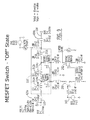
- Figure 4 illustrates a circuit simulation of the switch in the "on" state. Like numbers with Figure 2 are used. DC blocking capacitors 420a, 420b are also shown. A switch control input voltage of -20 V and a power supply voltage of 70 V are shown. Parasitic inductors are also shown for purposes of the simulation.
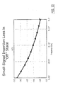
- Figure 5 graphically illustrates simulated small signal insertion loss in the "on" state for the MESFET switch of Figure 3. As shown, a loss of less than 0.25 dB is shown for frequencies between 20 MHz and 200 MHz.
- Figure 6 illustrates simulated loss in the "on” state versus RF input power as a function of frequency.
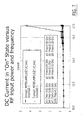
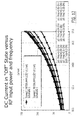
- Figure 7 illustrates simulated DC current in the "on” state versus RF input power and frequency.
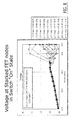
- Figure 8 illustrates the simulated voltage at the stacked FET nodes in the switch "on” state. In other words, Figure 8 illustrates that the voltage across the first and second power transistors 140', 142' are less than 50 volts between drain and source.
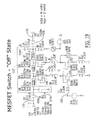
- Figure 9 is a circuit simulation of the switch of Figure 4 in the "off' state, where the power supply voltage VDD is switched to 0 V and the gate-to-source voltage corresponding to the switch control input 160 is switched to 2 V.
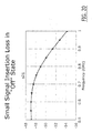
- Figure 10 graphically illustrates simulated small signal insertion loss in the "off' state
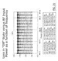
- Figure 11 illustrates simulated loss in the "off” state versus RF input power as a function of frequency.
- Figure 12 illustrates simulated DC current in the "off” state versus RF input power and frequency.
- Figure 13 illustrates the simulated voltage at the stacked FET nodes in the switch "off” state.
- Figures 4-13 show that some embodiments of the present invention that can provide at least 50 watts of power handling at less than 0.25 dB compression, an isolation of at least 32 dB and an effective on resistance of at least 0.5 ohm over a frequency range from about 20 MHz to about 200 MHz.
- Figures 14-23 refer to a second embodiment of a high power, high frequency silicon carbide MESFET switch that is capable of at least 50 watts power handling at less than about 0.3 dB compression, an isolation of at least 45 dB and an effective on resistance of less than 0.5 ohm over a frequency range of from about 500 MHz to about 1000 MHz.
- This embodiment was implemented using actual transmission lines 110" and shunt capacitors 314a, 314b, as was illustrated in Figure 3, but with two pairs of FETs 140', 250; and 142', 252 to absorb drain-to-source capacitance in shunt mode approach, as was illustrated in Figure 2. Stacked bare die FETs may be used to increase or maximize power handling.
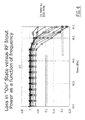
- Figure 14 illustrates this embodiment in the "on” state. Like numbers with Figures 2 and 3 are used. In the "on” state, a power supply voltage of 70 V and a control signal voltage 160 of -15 V is used.
- Figure 15 illustrates the simulated small signal insertion loss in the "on" state which is shown to be less than about 0.3 dB.
- Figure 16 illustrates simulated loss in the "on” state versus RF input power as a function of frequency.
- Figure 17 illustrates simulated DC current in the "on” state versus RF input power and frequency.
- Figure 18 illustrates simulated voltage at the stacked FET nodes in the "on” state, and shows voltage across the grounded gate FETs of less than 50 volts.
- Figure 19 shows the embodiment of Figure 14 in the "off" state, where a power supply voltage of 0 V and a control signal voltage of 2 V is provided.
- Figure 20 graphically illustrates simulated small signal insertion loss in the "off” state.
- Figure 21 illustrates simulated loss in the "off” state versus RF input power as a function of frequency.
- Figure 22 illustrates simulated DC current in the "off” state versus RF input power and frequency.
- Figure 23 illustrates simulated voltage at the stacked FET nodes in the switch "off' state.
- Figures 14-23 show that some embodiments of the invention can provide at least 50 watts of power handling at less than 0.3 dB compression, an isolation of at least 45 dB, and an effective on resistance of less than 0.5 ohm over a frequency range from about 500 MHz to about 1000 MHz.
- embodiments of the present invention have been described above in connection with single pole/single throw switches. However, embodiments of the present invention can be used for more complex switches with more poles/throws, such as a single pole/double throw switch.
- a schematic diagram of a simulated single pole/double throw switch is illustrated in Figure 24.
Abstract
Description
- This invention relates to electronic circuits, and more particularly to electronic switch circuits.
- Electronic switch circuits are widely used to switch high power (for example, at least 20 watts) at high frequencies (for example in the range of MHz and beyond). Semiconductor device manufacturers have developed transistors that are capable of operating at high frequencies and are still capable of handling higher power loads. For example, metal semiconductor field effect transistors (MESFETs) have been developed for high frequency, high power applications. High power, high frequency MESFETs have been fabricated from semiconductor materials including gallium arsenide, silicon carbide and/or gallium nitride.
- In order to provide a high power, high frequency switch, one or more power transistors, such as MESFETs, are connected into a circuit. It is desirable for such circuits to have a high power handling ability over a range of high frequencies, to provide relatively large isolation of the high power signal when in the "off" state, and relatively low resistance when in the "on" state.
- High power, high frequency switches according to some embodiments of the present invention include a transmission line having at least three portions that are serially coupled between an input port and an output port, to define at least two nodes therebetween, and to carry a high power, high frequency signal between the input port and the output port. First and second power transistors are provided, each including a controlling electrode and controlled electrodes. At least a third power transistor is also provided, including a controlling electrode and controlled electrodes. The controlled electrodes of a respective one of the first and second power transistors and of a respective one of the at least a third power transistor are serially coupled between a respective one of the at least two nodes and a reference voltage. The controlling electrodes of the first, second and/or at least a third power transistor are responsive to a switch control input. In some embodiments, the first, second and the at least a third power transistor are operable to shunt the first and second nodes to the reference voltage, and to decouple from the nodes, in response to the switch control signal.
- In some embodiments, the at least a third power transistor comprises a third and a fourth power transistor. The controlled electrodes of the first and third power transistors are serially connected between the first node and the reference voltage, and the controlled electrodes of the second and fourth power transistors are serially connected between the second node and the reference voltage.
- In still other embodiments, the at least a third power transistor consists of a third power transistor. The controlled electrodes of a respective one of the first and second power transistors and the third power transistor are serially coupled between the respective one of the at least two nodes and the reference voltage.
- In some embodiments, the transmission line comprises an actual transmission line including the at least three portions. The transmission line may include strip lines, coaxial lines and/or other conventional transmission lines. In other embodiments, the transmission line comprises an artificial transmission line that is formed of, for example, distributed series inductors and distributed shunt capacitors. In some embodiments, the shunt capacitors comprise parasitic capacitance of the first and second power transistors.
- High power, high frequency switches according to other embodiments of the present invention include a signal line that carries a high power, high frequency signal between an input port and an output port, and a plurality of strings of serially connected power transistors. A respective string of serially connected power transistors is connected between the signal line and a reference voltage, and is responsive to a switch control signal. In some embodiments, the plurality of strings of serially connected power transistors are operable to shunt to the signal line to the reference voltage, and to decouple from the signal line, in response to the switch control signal.
- In some embodiments, the above-described power transistors are embodied as silicon carbide MESFETs. Moreover, in some embodiments, the above-described circuits are configured to provide at least 50 watts of power handling at less than 0.25 dB compression, an isolation of at least 32 dB and an effective on resistance of less than 0.5 ohm over a frequency range of from about 20 MHz to about 200 MHz. In other embodiments, the above-described circuits are configured to provide at least 50 watts of power handling at less than 0.3 dB compression, an isolation of at least 45 dB and an effective on resistance of less than 0.5 ohm over a frequency range from about 500 MHz to about 1000 MHz.
- Figure 1 is a block diagram of a high power, high frequency switch according to various embodiments of the present invention.
- Figures 2 and 3 are circuit diagrams of high power, high frequency switches according to various embodiments of the present invention.
- Figure 4 is a circuit simulation of a high power, high frequency switch according to some embodiments of the present invention in the "on" state.
- Figures 5-8 graphically illustrate simulation results for the circuit of Figure 4.
- Figure 9 is a circuit simulation of a high power, high frequency switch according to some embodiments of the present invention in the "off" state.
- Figures 10-13 graphically illustrate simulation results for the circuit of Figure 9.
- Figure 14 is a circuit simulation of a high power, high frequency switch according to other embodiments of the present invention in the "on" state.
- Figures 15-18 graphically illustrate simulation results for the circuit of Figure 14.
- Figure 19 is a circuit simulation of a high power, high frequency switch according to other embodiments of the present invention in the "off" state.
- Figures 20-23 graphically illustrate simulation results for the circuit of Figure 19.
- Figure 24 is a circuit simulation of a single pole/double throw switch according to other embodiments of the present invention.
- The invention now will be described more fully hereinafter with reference to the accompanying drawings, in which embodiments of the invention are shown. This invention may, however, be embodied in many different forms and should not be construed as limited to the embodiments set forth herein. Rather, these embodiments are provided so that this disclosure will be thorough and complete, and will fully convey the scope of the invention to those skilled in the art. Moreover, each embodiment described and illustrated herein includes its complementary conductivity type embodiment as well. Like numbers refer to like elements throughout.
- It will be understood that when an element is referred to as being "connected", "coupled", "responsive" or "in response to" another element, it can be directly connected, responsive or in response to the other element or intervening elements may be present. In contrast, the term "directly" means there are no intervening elements present. As used herein, the term "and/or" includes any and all combinations of one or more of the associated listed items and may be abbreviated as "/".
- It will be understood that, although the terms first, second, etc. may be used herein to describe various elements, these elements should not be limited by these terms. These terms are only used to distinguish one element from another. For example, a first transistor could be termed a second transistor, and, similarly, a second transistor could be termed a first transistor without departing from the teachings of the disclosure.
- The terminology used herein is for the purpose of describing particular embodiments only and is not intended to be limiting of the invention. As used herein, the singular forms "a", "an" and "the" are intended to include the plural forms as well, unless the context clearly indicates otherwise. It will be further understood that the terms "comprises," "comprising," "includes" and/or "including", when used in this specification, specify the presence of stated features, regions, integers, steps, operations, elements, and/or components, but do not preclude the presence or addition of one or more other features, regions, integers, steps, operations, elements, components, and/or groups thereof. In contrast, the phrase "the at least a third power transistor consists of a third power transistor", when used in the specification, specifies that only a single third power transistor is provided.
- Unless otherwise defined, all terms (including technical and scientific terms) used herein have the same meaning as commonly understood by one of ordinary skill in the art to which this invention belongs. It will be further understood that terms, such as those defined in commonly used dictionaries, should be interpreted as having a meaning that is consistent with their meaning in the context of the relevant art and the present disclosure, and will not be interpreted in an idealized or overly formal sense unless expressly so defined herein.
- Figure 1 is a block diagram of a high power, high frequency switch according to various embodiments of the present invention. As shown in Figure 1, these embodiments of high power,
high frequency switch 100 include atransmission line 110 including at least threetransmission line portions 112a-112c that are serially coupled between aninput port 120 and anoutput port 130 to define at least twonodes transmission line portions 112a-112e are also labeled TLP1-TLP3 in Figure 1. Thetransmission line 110 carries the high power, high frequency signal between theinput port 120 and theoutput port 130, in either or both directions. - Still referring to Figure 1, first and
second power transistors third power transistor 150 is also provided, including a controlling electrode and controlled electrodes. As illustrated in Figure 1, the controlled electrodes of a respective one of the first andsecond transistors third transistor 150, are serially coupled between a respective one of the at least twonodes respective power transistor respective node respective connections second power transistors third power transistor 150 is indicated by theconnections - Still referring to Figure 1, the controlling electrodes of the
first power transistor 140,second power transistor 142 and/or at least athird power transistor 150 is responsive to aswitch control input 160. In some embodiments, as shown in Figure 1, the controlling electrodes of the at least athird power transistor 150 are responsive to theswitch control input 160. In other embodiments, the controlling electrodes of thefirst power transistor 140 and/orsecond power transistor 142 is responsive to the switch control input. In still other embodiments, thefirst power transistor 140,second power transistor 142 and at least athird power transistor 150 are all responsive to theswitch control input 160. A given power transistor may be directly responsive to theswitch control input 160 or may be indirectly responsive to theswitch control input 160, for example by way of a voltage divider or other circuit. - Figure 2 is a circuit diagram of a high power, high frequency switch according to other embodiments of the present invention. As shown in Figure 2, in these
switches 200, the transmission line 110' comprises an artificial transmission line that includes distributedseries inductors 212a-212c, and distributed shunt capacitors. In Figure 2, the distributed shunt capacitors may be provided by the parasitic capacitance of the first andsecond power transistors second power transistors third power transistor 150 of Figure 1 comprises athird power transistor 250 and afourth power transistor 252. As shown in Figure 2, in these embodiments, the third andfourth power transistors third power transistors first node 114a and the reference voltage (here ground), as shown by theconnections 140a', 140b'. Finally, the controlled electrodes of the second andfourth power transistors second node 114b and the reference voltage, as shown by theconnections 142a', 142b'. In Figure 2, the third and fourth power transistors may also be embodied as MESFETs and, in some embodiments, as silicon carbide-based MESFETs. - Figure 3 illustrates yet other embodiments of the present invention. In a high power,
high frequency switch 300 of Figure 3, thetransmission line 110" comprises an actual transmission line including at least threetransmission lines Discrete shunt capacitors third power transistor 150 of Figure 1 consists of asingle power transistor 350 including a controlling electrode that is responsive to theswitch control input 160. As shown in Figure 3, the controlled electrodes of a respective one of the first andsecond transistors third transistor 350 are serially coupled between a respective one of the at least twonodes - It will be understood by those having skill in the art that various embodiments of Figures 1-3 may be combined in various combinations and subcombinations. For example, a single
third power transistor 350 and/or multiplethird power transistors actual transmission line 110" may be used with any of the embodiments. Theswitch control input 160 may also be connected to the first andsecond power transistors second nodes nodes switch control input 160. - High power, high frequency switches according to exemplary embodiments of the present invention may also be regarded as including a
signal line input port 120 and anoutput port 130. A plurality ofstrings signal line switch control signal 160. The strings may include independent transistors, as illustrated in Figure 2, or a given transistor may be shared by two or more strings, as illustrated in Figure 3. Moreover, embodiments of Figures 1-3 include only two transistors in a given string. However, three or more transistors also may be stacked in a given string. Finally, only two strings are shown in Figures 1-3. However, more than two strings may also be provided in other embodiments of the present invention. - As was described above, the power transistors of Figures 1-3 may be embodied by MESFETs and, in some embodiments, by silicon carbide MESFETs. Silicon carbide MESFETs are known to those having skill in the art and are described, for example, in
U.S. Patents 4,762,806 ;4,757,028 ;5,270,554 ;5,925,895 ;6,686,616 ;6,906,350 and6,956,239 . Also, devices such as those described inU.S. Patent Application Serial No. 10/977,054, filed on October 29, 2004 No. 10/977,227, filed on October 29, 2004 No. 11/012,553, filed on December 15, 2004 No. 11/157,356, filed on June 21, 2005 - Moreover, other high power and/or high frequency transistors, such as High Electron Mobility Transistors (HEMTs), also referred to as Modulation-Doped Field Effect Transistors (MODFETs), may be used. For example, HEMTs, as described in
U.S. Patents 5,192,987 ;5,296,395 ;6,316,793 ;6,548,333 ; and6,849,882 may be used. Other suitable structures for gallium nitride-based HEMTs are described, for example, inU.S. Patent Publication No. 2004/0061129 filed July 11, 2003 and published April 1, 2004 for Nitride-Based Transistors And Methods Of Fabrication Thereof Using Non-Etched Contact Recesses;U.S. Patent Publication No. 2003/0020092 filed July 23, 2002 and published January 30, 2003 for Insulating Gate AlGaN/GaN HEMT;U.S. Application Serial No. 11/118,575, filed April 29, 2005 U.S. Application Serial No. 11/118,675, filed April 29, 2005 - Accordingly, some embodiments of the invention can employ pairs of silicon carbide MESFETs in an artificial/actual transmission line configuration, such that the drain and gate voltages on the MESFETs are changed to provide a low loss (or even some gain) "on" state or a high isolation "off" state. Stacked MESFETs may be used to increase or maximize radio frequency (RF) power handling ability at low frequencies, by providing the voltage swing across the gates of the devices. Suitable gate width FETs may be used to enable RF power handling with low compression. Some embodiments of the invention can provide a high power, high isolation switch covering a decade of bandwidth at relatively low current drive. Embodiments of the invention may also be compatible with standard Monolithic Microwave Integrated Circuit (MMIC) design practices, which can allow the potential integration of the switch configurations of embodiments of the present invention with other circuit elements, such as power amplifiers.
- Conventionally, switches for the same levels of RF power handling capacities may employ PIN diodes, which may draw large amounts of current in their "on" states and may not be compatible with MMIC technology. In sharp contrast, some embodiments of the invention can use multiple FETs in an actual/artificial transmission line configuration and/or may employ stacked transistors to allow greater power handling capability, particularly at low frequencies, where the low parasitic capacitance of the transistors may not contribute to the effective voltage division between the gate and drain, and the gate and source.
- Some embodiments of the present invention can provide a 20 MHz to 200 MHz single pole/single throw switch. Moreover, other embodiments of the invention can be scaled in power handling and/or frequency, to cover specific bandwidths. The single pole/single throw switch configuration also may provide a building block for many other switch configurations, such as multiple pole/multiple throw switches.
- Embodiments of the invention can exhibit well behaved compression characteristics in the "on" state, where simulations indicate only 0.2 dB loss at 56 watts continuous wave power, as described below. Low switch loss at high power levels can be used to reduce or minimize dissipated power/heat, increase or maximize system efficiency, etc. Other embodiments of the present invention can replace the series inductors of Figure 2 with actual transmission lines, as in Figure 3. Actual transmission lines may be used in higher frequency applications, in some embodiments of the present invention.
- As will be described in detail below, in some embodiments of the present invention, the
transmission line third transistors - The following Examples shall be regarded as merely illustrative and shall not be construed as limiting the invention. Two embodiments of high power, high frequency switches were designed and simulated, as will be described in detail below. A conventional Harmonic Balance Nonlinear simulator, such as Applied Wave Research's "Microwave Office Version 6.53 ", was used to simulate these circuits.
- Example 1
- Figures 4-13 refer to a first high power, high frequency switch according to exemplary embodiments of the present invention. These embodiments are capable of more than 50 watts power handling at less than 0.25 dB compression. An isolation of at least 32 dB is provided over a bandwidth from about 20 MHz to about 200 MHz. The effective"on"resistance is less than about 0.5 ohm. These embodiments are implemented using an artificial transmission line with two pairs of silicon carbide MESFETs, to absorb the drain-to-source capacitance in shunt mode approach, as was illustrated schematically in Figure 2. In some embodiments, stacked bare die silicon carbide MESFETs may be used to increase or maximize power handling ability at low frequencies.
- Figure 4 illustrates a circuit simulation of the switch in the "on" state. Like numbers with Figure 2 are used.
DC blocking capacitors - Figure 5 graphically illustrates simulated small signal insertion loss in the "on" state for the MESFET switch of Figure 3. As shown, a loss of less than 0.25 dB is shown for frequencies between 20 MHz and 200 MHz.
- Figure 6 illustrates simulated loss in the "on" state versus RF input power as a function of frequency. Figure 7 illustrates simulated DC current in the "on" state versus RF input power and frequency. Figure 8 illustrates the simulated voltage at the stacked FET nodes in the switch "on" state. In other words, Figure 8 illustrates that the voltage across the first and
second power transistors - Figure 9 is a circuit simulation of the switch of Figure 4 in the "off' state, where the power supply voltage VDD is switched to 0 V and the gate-to-source voltage corresponding to the
switch control input 160 is switched to 2 V. Figure 10 graphically illustrates simulated small signal insertion loss in the "off' state, and Figure 11 illustrates simulated loss in the "off" state versus RF input power as a function of frequency. Figure 12 illustrates simulated DC current in the "off" state versus RF input power and frequency. Finally, Figure 13 illustrates the simulated voltage at the stacked FET nodes in the switch "off" state. - Accordingly, Figures 4-13 show that some embodiments of the present invention that can provide at least 50 watts of power handling at less than 0.25 dB compression, an isolation of at least 32 dB and an effective on resistance of at least 0.5 ohm over a frequency range from about 20 MHz to about 200 MHz.
- Example 2
- Figures 14-23 refer to a second embodiment of a high power, high frequency silicon carbide MESFET switch that is capable of at least 50 watts power handling at less than about 0.3 dB compression, an isolation of at least 45 dB and an effective on resistance of less than 0.5 ohm over a frequency range of from about 500 MHz to about 1000 MHz. This embodiment was implemented using
actual transmission lines 110" andshunt capacitors FETs - Figure 14 illustrates this embodiment in the "on" state. Like numbers with Figures 2 and 3 are used. In the "on" state, a power supply voltage of 70 V and a
control signal voltage 160 of -15 V is used. - Figure 15 illustrates the simulated small signal insertion loss in the "on" state which is shown to be less than about 0.3 dB. Figure 16 illustrates simulated loss in the "on" state versus RF input power as a function of frequency. Figure 17 illustrates simulated DC current in the "on" state versus RF input power and frequency. Figure 18 illustrates simulated voltage at the stacked FET nodes in the "on" state, and shows voltage across the grounded gate FETs of less than 50 volts.
- Figure 19 shows the embodiment of Figure 14 in the "off" state, where a power supply voltage of 0 V and a control signal voltage of 2 V is provided.
- Figure 20 graphically illustrates simulated small signal insertion loss in the "off" state. Figure 21 illustrates simulated loss in the "off" state versus RF input power as a function of frequency. Figure 22 illustrates simulated DC current in the "off" state versus RF input power and frequency. Figure 23 illustrates simulated voltage at the stacked FET nodes in the switch "off' state.
- Accordingly, Figures 14-23 show that some embodiments of the invention can provide at least 50 watts of power handling at less than 0.3 dB compression, an isolation of at least 45 dB, and an effective on resistance of less than 0.5 ohm over a frequency range from about 500 MHz to about 1000 MHz.
- Finally, embodiments of the present invention have been described above in connection with single pole/single throw switches. However, embodiments of the present invention can be used for more complex switches with more poles/throws, such as a single pole/double throw switch. A schematic diagram of a simulated single pole/double throw switch is illustrated in Figure 24.
- In the drawings and specification, there have been disclosed embodiments of the invention and, although specific terms are employed, they are used in a generic and descriptive sense only and not for purposes of limitation, the scope of the invention being set forth in the following claims.
Claims (20)
- A high power, high frequency switch (100, 200, 300) comprising:a transmission line (110, 110', 110") including at least three portions (112a-c, 212a-c, 312 a-c) that are serially coupled between an input port (120) and an output port (130) to define at least two nodes (114a, 114b) therebetween, and to carry a high power, high frequency signal between the input port (120) and the output port (130);first and second power transistors (140, 140', 140"; 142, 142', 142") including a controlling electrode and controlled electrodes; andat least a third power transistor (150) including a controlling electrode and also controlled electrodes, the controlled electrodes of a respective one of the first and second power transistors and of a respective one of the at least a third power transistor being serially coupled between a respective one of the at least two nodes and a reference voltage, the controlling electrodes of the first, second and/or at least a third power transistor being responsive to a switch control input (160).
- A switch according to Claim 1 wherein the at least a third power transistor (150) comprises a third (250) and a fourth (252) power transistor, the controlled electrodes of the first and third power transistors being serially connected between the first node and the reference voltage and the controlled electrodes of the second and fourth power transistors being serially connected between the second node and the reference voltage.
- A switch according to Claim 1 wherein the at least a third power transistor (150) consists of a third power transistor (350), the controlled electrodes of a respective one of the first and second power transistors and the third power transistor (350) being serially coupled between the respective one of the at least two nodes (114a, 114b) and the reference voltage.
- A switch according to Claim 1, 2 or 3 wherein first (140, 140', 140") second (142, 142', 142") and the at least a third power transistor (150) are operable to shunt the first (114a) and second (114b) nodes to the reference voltage and to decouple from the nodes in response to the switch control input (160).
- A switch according to Claim 1 or 3 wherein the transmission line comprises an actual transmission line including at least three portions (112a, 112b, 112c; 312a, 312b,312c).
- A switch according to Claim 1 or 2 wherein the transmission line comprises an artificial transmission line (110') comprising distributed series inductors (212a-212c) and distributed shunt capacitors.
- A switch according to Claim 6 wherein the shunt capacitors comprise parasitic capacitance of the first (140') and second (142') power transistors.
- A switch according to any preceding Claim, wherein the controlling electrodes of the first and second power transistors are coupled to a reference voltage and wherein the controlling electrodes of the at least a third power transistor are coupled to the switch control input.
- A switch according to any preceding Claim, wherein the first, second and the at least a third power transistors are silicon carbide MESFETS.
- A switch according to any Claim 1 to 9 wherein the transmission line and the first, second and the at least a third power transistors are configured to provide at least 50 watts of power handling at less than 0.25 dB compression, an isolation of at least 32 dB and an effective on resistance of less than 0.5 ohm over a range from about 20 MHz to about 200 MHz.
- A switch according to any Claim 1 to 9 wherein the transmission line and the first, second and the at least a third power transistors are configured to provide at least 50 watts of power handling at less than 0.3 dB compression, an isolation of at least 45 dB and an effective on resistance of less than 0.5 ohm over a range from about 500 MHz to about 1000 MHz.
- A high power, high frequency switch (100, 200, 300) comprising:a signal line (110, 110', 110") that carries a high power, high frequency signal between an input port (120) and an output port (130); anda plurality of strings (170a-c; 170a' -c'; 170a" -c") of serially connected power transistors, a respective string of serially connected power transistors being connected between the signal line and a reference voltage and being responsive to a switch control signal (160).
- A switch according to Claim 12 wherein the plurality of strings of serially connected power transistors are operable to shunt the signal line to the reference voltage and to decouple from the signal line in response to the switch control signal.
- A switch according to Claim 12 wherein the signal line comprises an artificial and/or an actual transmission line.
- A switch according to any Claim 12 to 14 wherein the power transistors comprise silicon carbide MESFETs.
- A switch according to any Claim 12 to 15 wherein the plurality of strings of serially connected power transistors are configured to provide at least 50 watts of power handling at less than 0.25 dB compression, an isolation of at least 32 dB and an effective on resistance of less than 0.5 ohm over a range from about 20 MHz to about 200 MHz.
- A switch according to any Claim 12 to 15 wherein the plurality of strings of serially connected power transistors are configured to provide at least 50 watts of power handling at less than 0.3 dB compression, an isolation of at least 45 dB and an effective on resistance of less than 0.5 ohm over a range from about 500 MHz to about 1000 MHz.
- A high power, high frequency switch (100, 200, 300) comprising:a signal line (110, 110', 110") that carries a high power, high frequency signal between an input port (120) and an output port (130); anda plurality of power transistors that are connected to the signal line (110, 110', 110") and are responsive to a switch control signal (160), the plurality of power transistors being operable to provide at least 50 watts of power handling at less than 0.3 dB compression, an isolation of at least 45 dB and an affective on resistance of less than 0.5 ohm over a range from about 500 MHz to about 1000 MHz.
- A switch according to Claim 18 wherein the signal line (110, 110', 110") comprises an artificial and/or an actual transmission line.
- A switch according to Claim 18 wherein the power transistors comprise silicon carbide MESFETs.
Applications Claiming Priority (1)
| Application Number | Priority Date | Filing Date | Title |
|---|---|---|---|
| US11/295,060 US7368971B2 (en) | 2005-12-06 | 2005-12-06 | High power, high frequency switch circuits using strings of power transistors |
Publications (2)
| Publication Number | Publication Date |
|---|---|
| EP1796202A1 true EP1796202A1 (en) | 2007-06-13 |
| EP1796202B1 EP1796202B1 (en) | 2013-07-10 |
Family
ID=37806956
Family Applications (1)
| Application Number | Title | Priority Date | Filing Date |
|---|---|---|---|
| EP06124121.2A Active EP1796202B1 (en) | 2005-12-06 | 2006-11-15 | High power, high frequency switch circuits using strings of power transistors |
Country Status (2)
| Country | Link |
|---|---|
| US (1) | US7368971B2 (en) |
| EP (1) | EP1796202B1 (en) |
Families Citing this family (8)
| Publication number | Priority date | Publication date | Assignee | Title |
|---|---|---|---|---|
| FR2931300B1 (en) * | 2008-05-16 | 2016-10-21 | Thales Sa | HYPERFREQUENCY SWITCH AND TRANSMITTING AND RECEIVING MODULE HAVING SUCH A SWITCH |
| US7764120B2 (en) * | 2008-08-19 | 2010-07-27 | Cree, Inc. | Integrated circuit with parallel sets of transistor amplifiers having different turn on power levels |
| US7893791B2 (en) | 2008-10-22 | 2011-02-22 | The Boeing Company | Gallium nitride switch methodology |
| US8390395B2 (en) | 2010-05-03 | 2013-03-05 | Raytheon Company | High power RF switch with active device size tapering |
| US8421122B2 (en) * | 2010-05-20 | 2013-04-16 | Cree, Inc. | High power gallium nitride field effect transistor switches |
| US8436643B2 (en) | 2010-11-04 | 2013-05-07 | Advanced Energy Industries, Inc. | High frequency solid state switching for impedance matching |
| US9065426B2 (en) | 2011-11-03 | 2015-06-23 | Advanced Energy Industries, Inc. | High frequency solid state switching for impedance matching |
| US10027366B2 (en) * | 2014-04-25 | 2018-07-17 | Raytheon Company | High power radio frequency (RF) antenna switch |
Citations (3)
| Publication number | Priority date | Publication date | Assignee | Title |
|---|---|---|---|---|
| US5666089A (en) | 1996-04-12 | 1997-09-09 | Hewlett-Packard Company | Monolithic step attenuator having internal frequency compensation |
| US5990580A (en) * | 1998-03-05 | 1999-11-23 | The Whitaker Corporation | Single pole double throw switch |
| US20030132814A1 (en) * | 2002-01-15 | 2003-07-17 | Nokia Corporation | Circuit topology for attenuator and switch circuits |
Family Cites Families (17)
| Publication number | Priority date | Publication date | Assignee | Title |
|---|---|---|---|---|
| US4762806A (en) | 1983-12-23 | 1988-08-09 | Sharp Kabushiki Kaisha | Process for producing a SiC semiconductor device |
| JP2615390B2 (en) | 1985-10-07 | 1997-05-28 | 工業技術院長 | Method of manufacturing silicon carbide field effect transistor |
| US5081706A (en) * | 1987-07-30 | 1992-01-14 | Texas Instruments Incorporated | Broadband merged switch |
| US4929855A (en) * | 1988-12-09 | 1990-05-29 | Grumman Corporation | High frequency switching device |
| US5012123A (en) * | 1989-03-29 | 1991-04-30 | Hittite Microwave, Inc. | High-power rf switching system |
| US5192987A (en) | 1991-05-17 | 1993-03-09 | Apa Optics, Inc. | High electron mobility transistor with GaN/Alx Ga1-x N heterojunctions |
| US5270554A (en) | 1991-06-14 | 1993-12-14 | Cree Research, Inc. | High power high frequency metal-semiconductor field-effect transistor formed in silicon carbide |
| US5925895A (en) | 1993-10-18 | 1999-07-20 | Northrop Grumman Corporation | Silicon carbide power MESFET with surface effect supressive layer |
| JPH0927736A (en) * | 1995-07-13 | 1997-01-28 | Japan Radio Co Ltd | Fet switch |
| US6316793B1 (en) | 1998-06-12 | 2001-11-13 | Cree, Inc. | Nitride based transistors on semi-insulating silicon carbide substrates |
| US6686616B1 (en) | 2000-05-10 | 2004-02-03 | Cree, Inc. | Silicon carbide metal-semiconductor field effect transistors |
| US6548333B2 (en) | 2000-12-01 | 2003-04-15 | Cree, Inc. | Aluminum gallium nitride/gallium nitride high electron mobility transistors having a gate contact on a gallium nitride based cap segment |
| US6849882B2 (en) | 2001-05-11 | 2005-02-01 | Cree Inc. | Group-III nitride based high electron mobility transistor (HEMT) with barrier/spacer layer |
| WO2003032397A2 (en) | 2001-07-24 | 2003-04-17 | Cree, Inc. | INSULTING GATE AlGaN/GaN HEMT |
| US6906350B2 (en) | 2001-10-24 | 2005-06-14 | Cree, Inc. | Delta doped silicon carbide metal-semiconductor field effect transistors having a gate disposed in a double recess structure |
| US6982204B2 (en) | 2002-07-16 | 2006-01-03 | Cree, Inc. | Nitride-based transistors and methods of fabrication thereof using non-etched contact recesses |
| US6956239B2 (en) | 2002-11-26 | 2005-10-18 | Cree, Inc. | Transistors having buried p-type layers beneath the source region |
-
2005
- 2005-12-06 US US11/295,060 patent/US7368971B2/en active Active
-
2006
- 2006-11-15 EP EP06124121.2A patent/EP1796202B1/en active Active
Patent Citations (3)
| Publication number | Priority date | Publication date | Assignee | Title |
|---|---|---|---|---|
| US5666089A (en) | 1996-04-12 | 1997-09-09 | Hewlett-Packard Company | Monolithic step attenuator having internal frequency compensation |
| US5990580A (en) * | 1998-03-05 | 1999-11-23 | The Whitaker Corporation | Single pole double throw switch |
| US20030132814A1 (en) * | 2002-01-15 | 2003-07-17 | Nokia Corporation | Circuit topology for attenuator and switch circuits |
Non-Patent Citations (1)
| Title |
|---|
| UMEDA Y ET AL INSTITUTE OF ELECTRICAL AND ELECTRONICS ENGINEERS: "Novel direct-coupled current switch architecture for a series-connected voltage-balancing pulse driver", 2003 IEEE MTT-S INTERNATIONAL MICROWAVE SYMPOSIUM DIGEST.(IMS 2003). PHILADELPHIA, PA, JUNE 8 - 13, 2003, IEEE MTT-S INTERNATIONAL MICROWAVE SYMPOSIUM, NEW YORK, NY : IEEE, US, vol. VOL. 3 OF 3, 8 June 2003 (2003-06-08), pages 2265 - 2268, XP010746706, ISBN: 0-7803-7695-1 * |
Also Published As
| Publication number | Publication date |
|---|---|
| EP1796202B1 (en) | 2013-07-10 |
| US7368971B2 (en) | 2008-05-06 |
| US20070126492A1 (en) | 2007-06-07 |
Similar Documents
| Publication | Publication Date | Title |
|---|---|---|
| EP1796202B1 (en) | High power, high frequency switch circuits using strings of power transistors | |
| US7561853B2 (en) | Radio frequency switch | |
| US7928794B2 (en) | Method and apparatus for a dynamically self-bootstrapped switch | |
| US8421122B2 (en) | High power gallium nitride field effect transistor switches | |
| US20010040479A1 (en) | Electronic switch | |
| US7893749B2 (en) | High frequency switch circuit having reduced input power distortion | |
| US8614597B2 (en) | High linear voltage variable attenuator (VVA) | |
| US5945879A (en) | Series-connected microwave power amplifiers with voltage feedback and method of operation for the same | |
| CN109792234A (en) | The ontology of stacked transistors amplifier links optimization | |
| US20230283247A1 (en) | Device Stack with Novel Gate Capacitor Topology | |
| US20170047924A1 (en) | Power switching cell with normally conducting field-effect transistors | |
| US11323072B1 (en) | Mixer with series connected active devices | |
| CN107078722B (en) | Active circulator with radio frequency choke | |
| Huang et al. | A 20-mW G-band monolithic driver amplifier using 0.07-μm InP HEMT | |
| JP2008147627A (en) | High isolation switching element for millimeter wave band control circuit | |
| JP5011312B2 (en) | Method and system for high power switching | |
| Dennler et al. | Monolithic three-stage 6–18GHz high power amplifier with distributed interstage in GaN technology | |
| US20080106353A1 (en) | High-frequency switch | |
| US6774416B2 (en) | Small area cascode FET structure operating at mm-wave frequencies | |
| US20090079489A1 (en) | Constant phase digital attenuator with on-chip matching circuitry | |
| Koudymov et al. | Monolithically integrated high-power broad-band RF switch based on III-N insulated gate transistors | |
| US8039880B2 (en) | High performance microwave switching devices and circuits | |
| Campbell et al. | Design considerations for GaN based MMICs | |
| WO2010127078A1 (en) | Transistor junction diode circuitry systems and methods | |
| CN111934663A (en) | Transfer printing for radio frequency applications |
Legal Events
| Date | Code | Title | Description |
|---|---|---|---|
| PUAI | Public reference made under article 153(3) epc to a published international application that has entered the european phase |
Free format text: ORIGINAL CODE: 0009012 |
|
| AK | Designated contracting states |
Kind code of ref document: A1 Designated state(s): AT BE BG CH CY CZ DE DK EE ES FI FR GB GR HU IE IS IT LI LT LU LV MC NL PL PT RO SE SI SK TR |
|
| AX | Request for extension of the european patent |
Extension state: AL BA HR MK YU |
|
| 17P | Request for examination filed |
Effective date: 20071203 |
|
| 17Q | First examination report despatched |
Effective date: 20080109 |
|
| AKX | Designation fees paid |
Designated state(s): AT BE BG CH CY CZ DE DK EE ES FI FR GB GR HU IE IS IT LI LT LU LV MC NL PL PT RO SE SI SK TR |
|
| GRAP | Despatch of communication of intention to grant a patent |
Free format text: ORIGINAL CODE: EPIDOSNIGR1 |
|
| GRAP | Despatch of communication of intention to grant a patent |
Free format text: ORIGINAL CODE: EPIDOSNIGR1 |
|
| GRAP | Despatch of communication of intention to grant a patent |
Free format text: ORIGINAL CODE: EPIDOSNIGR1 |
|
| GRAP | Despatch of communication of intention to grant a patent |
Free format text: ORIGINAL CODE: EPIDOSNIGR1 |
|
| INTG | Intention to grant announced |
Effective date: 20130424 |
|
| GRAS | Grant fee paid |
Free format text: ORIGINAL CODE: EPIDOSNIGR3 |
|
| GRAA | (expected) grant |
Free format text: ORIGINAL CODE: 0009210 |
|
| INTG | Intention to grant announced |
Effective date: 20130514 |
|
| AK | Designated contracting states |
Kind code of ref document: B1 Designated state(s): AT BE BG CH CY CZ DE DK EE ES FI FR GB GR HU IE IS IT LI LT LU LV MC NL PL PT RO SE SI SK TR |
|
| REG | Reference to a national code |
Ref country code: GB Ref legal event code: FG4D |
|
| REG | Reference to a national code |
Ref country code: CH Ref legal event code: EP Ref country code: AT Ref legal event code: REF Ref document number: 621418 Country of ref document: AT Kind code of ref document: T Effective date: 20130715 |
|
| REG | Reference to a national code |
Ref country code: IE Ref legal event code: FG4D |
|
| REG | Reference to a national code |
Ref country code: DE Ref legal event code: R096 Ref document number: 602006037202 Country of ref document: DE Effective date: 20130905 |
|
| PG25 | Lapsed in a contracting state [announced via postgrant information from national office to epo] |
Ref country code: SI Free format text: LAPSE BECAUSE OF FAILURE TO SUBMIT A TRANSLATION OF THE DESCRIPTION OR TO PAY THE FEE WITHIN THE PRESCRIBED TIME-LIMIT Effective date: 20130710 |
|
| REG | Reference to a national code |
Ref country code: AT Ref legal event code: MK05 Ref document number: 621418 Country of ref document: AT Kind code of ref document: T Effective date: 20130710 |
|
| REG | Reference to a national code |
Ref country code: NL Ref legal event code: VDEP Effective date: 20130710 |
|
| REG | Reference to a national code |
Ref country code: LT Ref legal event code: MG4D |
|
| PG25 | Lapsed in a contracting state [announced via postgrant information from national office to epo] |
Ref country code: CY Free format text: LAPSE BECAUSE OF FAILURE TO SUBMIT A TRANSLATION OF THE DESCRIPTION OR TO PAY THE FEE WITHIN THE PRESCRIBED TIME-LIMIT Effective date: 20130717 Ref country code: IS Free format text: LAPSE BECAUSE OF FAILURE TO SUBMIT A TRANSLATION OF THE DESCRIPTION OR TO PAY THE FEE WITHIN THE PRESCRIBED TIME-LIMIT Effective date: 20131110 Ref country code: SE Free format text: LAPSE BECAUSE OF FAILURE TO SUBMIT A TRANSLATION OF THE DESCRIPTION OR TO PAY THE FEE WITHIN THE PRESCRIBED TIME-LIMIT Effective date: 20130710 Ref country code: PT Free format text: LAPSE BECAUSE OF FAILURE TO SUBMIT A TRANSLATION OF THE DESCRIPTION OR TO PAY THE FEE WITHIN THE PRESCRIBED TIME-LIMIT Effective date: 20131111 Ref country code: AT Free format text: LAPSE BECAUSE OF FAILURE TO SUBMIT A TRANSLATION OF THE DESCRIPTION OR TO PAY THE FEE WITHIN THE PRESCRIBED TIME-LIMIT Effective date: 20130710 Ref country code: LT Free format text: LAPSE BECAUSE OF FAILURE TO SUBMIT A TRANSLATION OF THE DESCRIPTION OR TO PAY THE FEE WITHIN THE PRESCRIBED TIME-LIMIT Effective date: 20130710 Ref country code: BE Free format text: LAPSE BECAUSE OF FAILURE TO SUBMIT A TRANSLATION OF THE DESCRIPTION OR TO PAY THE FEE WITHIN THE PRESCRIBED TIME-LIMIT Effective date: 20130710 |
|
| PG25 | Lapsed in a contracting state [announced via postgrant information from national office to epo] |
Ref country code: NL Free format text: LAPSE BECAUSE OF FAILURE TO SUBMIT A TRANSLATION OF THE DESCRIPTION OR TO PAY THE FEE WITHIN THE PRESCRIBED TIME-LIMIT Effective date: 20130710 Ref country code: GR Free format text: LAPSE BECAUSE OF FAILURE TO SUBMIT A TRANSLATION OF THE DESCRIPTION OR TO PAY THE FEE WITHIN THE PRESCRIBED TIME-LIMIT Effective date: 20131011 Ref country code: ES Free format text: LAPSE BECAUSE OF FAILURE TO SUBMIT A TRANSLATION OF THE DESCRIPTION OR TO PAY THE FEE WITHIN THE PRESCRIBED TIME-LIMIT Effective date: 20131021 Ref country code: LV Free format text: LAPSE BECAUSE OF FAILURE TO SUBMIT A TRANSLATION OF THE DESCRIPTION OR TO PAY THE FEE WITHIN THE PRESCRIBED TIME-LIMIT Effective date: 20130710 Ref country code: PL Free format text: LAPSE BECAUSE OF FAILURE TO SUBMIT A TRANSLATION OF THE DESCRIPTION OR TO PAY THE FEE WITHIN THE PRESCRIBED TIME-LIMIT Effective date: 20130710 |
|
| PG25 | Lapsed in a contracting state [announced via postgrant information from national office to epo] |
Ref country code: CY Free format text: LAPSE BECAUSE OF FAILURE TO SUBMIT A TRANSLATION OF THE DESCRIPTION OR TO PAY THE FEE WITHIN THE PRESCRIBED TIME-LIMIT Effective date: 20130710 |
|
| PG25 | Lapsed in a contracting state [announced via postgrant information from national office to epo] |
Ref country code: SK Free format text: LAPSE BECAUSE OF FAILURE TO SUBMIT A TRANSLATION OF THE DESCRIPTION OR TO PAY THE FEE WITHIN THE PRESCRIBED TIME-LIMIT Effective date: 20130710 Ref country code: CZ Free format text: LAPSE BECAUSE OF FAILURE TO SUBMIT A TRANSLATION OF THE DESCRIPTION OR TO PAY THE FEE WITHIN THE PRESCRIBED TIME-LIMIT Effective date: 20130710 Ref country code: DK Free format text: LAPSE BECAUSE OF FAILURE TO SUBMIT A TRANSLATION OF THE DESCRIPTION OR TO PAY THE FEE WITHIN THE PRESCRIBED TIME-LIMIT Effective date: 20130710 Ref country code: RO Free format text: LAPSE BECAUSE OF FAILURE TO SUBMIT A TRANSLATION OF THE DESCRIPTION OR TO PAY THE FEE WITHIN THE PRESCRIBED TIME-LIMIT Effective date: 20130710 Ref country code: EE Free format text: LAPSE BECAUSE OF FAILURE TO SUBMIT A TRANSLATION OF THE DESCRIPTION OR TO PAY THE FEE WITHIN THE PRESCRIBED TIME-LIMIT Effective date: 20130710 |
|
| PLBE | No opposition filed within time limit |
Free format text: ORIGINAL CODE: 0009261 |
|
| STAA | Information on the status of an ep patent application or granted ep patent |
Free format text: STATUS: NO OPPOSITION FILED WITHIN TIME LIMIT |
|
| PG25 | Lapsed in a contracting state [announced via postgrant information from national office to epo] |
Ref country code: IT Free format text: LAPSE BECAUSE OF FAILURE TO SUBMIT A TRANSLATION OF THE DESCRIPTION OR TO PAY THE FEE WITHIN THE PRESCRIBED TIME-LIMIT Effective date: 20130710 |
|
| 26N | No opposition filed |
Effective date: 20140411 |
|
| REG | Reference to a national code |
Ref country code: CH Ref legal event code: PL |
|
| GBPC | Gb: european patent ceased through non-payment of renewal fee |
Effective date: 20131115 |
|
| REG | Reference to a national code |
Ref country code: DE Ref legal event code: R097 Ref document number: 602006037202 Country of ref document: DE Effective date: 20140411 |
|
| PG25 | Lapsed in a contracting state [announced via postgrant information from national office to epo] |
Ref country code: MC Free format text: LAPSE BECAUSE OF FAILURE TO SUBMIT A TRANSLATION OF THE DESCRIPTION OR TO PAY THE FEE WITHIN THE PRESCRIBED TIME-LIMIT Effective date: 20130710 Ref country code: LI Free format text: LAPSE BECAUSE OF NON-PAYMENT OF DUE FEES Effective date: 20131130 Ref country code: CH Free format text: LAPSE BECAUSE OF NON-PAYMENT OF DUE FEES Effective date: 20131130 |
|
| REG | Reference to a national code |
Ref country code: IE Ref legal event code: MM4A |
|
| PG25 | Lapsed in a contracting state [announced via postgrant information from national office to epo] |
Ref country code: IE Free format text: LAPSE BECAUSE OF NON-PAYMENT OF DUE FEES Effective date: 20131115 |
|
| PG25 | Lapsed in a contracting state [announced via postgrant information from national office to epo] |
Ref country code: GB Free format text: LAPSE BECAUSE OF NON-PAYMENT OF DUE FEES Effective date: 20131115 |
|
| PG25 | Lapsed in a contracting state [announced via postgrant information from national office to epo] |
Ref country code: TR Free format text: LAPSE BECAUSE OF FAILURE TO SUBMIT A TRANSLATION OF THE DESCRIPTION OR TO PAY THE FEE WITHIN THE PRESCRIBED TIME-LIMIT Effective date: 20130710 |
|
| PG25 | Lapsed in a contracting state [announced via postgrant information from national office to epo] |
Ref country code: HU Free format text: LAPSE BECAUSE OF FAILURE TO SUBMIT A TRANSLATION OF THE DESCRIPTION OR TO PAY THE FEE WITHIN THE PRESCRIBED TIME-LIMIT; INVALID AB INITIO Effective date: 20061115 Ref country code: LU Free format text: LAPSE BECAUSE OF NON-PAYMENT OF DUE FEES Effective date: 20131115 Ref country code: BG Free format text: LAPSE BECAUSE OF FAILURE TO SUBMIT A TRANSLATION OF THE DESCRIPTION OR TO PAY THE FEE WITHIN THE PRESCRIBED TIME-LIMIT Effective date: 20130710 |
|
| REG | Reference to a national code |
Ref country code: FR Ref legal event code: PLFP Year of fee payment: 10 |
|
| REG | Reference to a national code |
Ref country code: FR Ref legal event code: PLFP Year of fee payment: 11 |
|
| REG | Reference to a national code |
Ref country code: FR Ref legal event code: PLFP Year of fee payment: 12 |
|
| REG | Reference to a national code |
Ref country code: FR Ref legal event code: PLFP Year of fee payment: 13 |
|
| PGFP | Annual fee paid to national office [announced via postgrant information from national office to epo] |
Ref country code: FR Payment date: 20231127 Year of fee payment: 18 Ref country code: FI Payment date: 20231127 Year of fee payment: 18 Ref country code: DE Payment date: 20231129 Year of fee payment: 18 |