EP1792364B1 - Spiral antenna - Google Patents
Spiral antenna Download PDFInfo
- Publication number
- EP1792364B1 EP1792364B1 EP05800801A EP05800801A EP1792364B1 EP 1792364 B1 EP1792364 B1 EP 1792364B1 EP 05800801 A EP05800801 A EP 05800801A EP 05800801 A EP05800801 A EP 05800801A EP 1792364 B1 EP1792364 B1 EP 1792364B1
- Authority
- EP
- European Patent Office
- Prior art keywords
- antenna
- arms
- spiral
- circuit board
- contact location
- Prior art date
- Legal status (The legal status is an assumption and is not a legal conclusion. Google has not performed a legal analysis and makes no representation as to the accuracy of the status listed.)
- Not-in-force
Links
Images


Classifications
-
- H—ELECTRICITY
- H01—ELECTRIC ELEMENTS
- H01Q—ANTENNAS, i.e. RADIO AERIALS
- H01Q1/00—Details of, or arrangements associated with, antennas
- H01Q1/36—Structural form of radiating elements, e.g. cone, spiral, umbrella; Particular materials used therewith
- H01Q1/38—Structural form of radiating elements, e.g. cone, spiral, umbrella; Particular materials used therewith formed by a conductive layer on an insulating support
-
- H—ELECTRICITY
- H01—ELECTRIC ELEMENTS
- H01Q—ANTENNAS, i.e. RADIO AERIALS
- H01Q1/00—Details of, or arrangements associated with, antennas
- H01Q1/12—Supports; Mounting means
- H01Q1/1207—Supports; Mounting means for fastening a rigid aerial element
- H01Q1/1221—Supports; Mounting means for fastening a rigid aerial element onto a wall
-
- H—ELECTRICITY
- H01—ELECTRIC ELEMENTS
- H01Q—ANTENNAS, i.e. RADIO AERIALS
- H01Q1/00—Details of, or arrangements associated with, antennas
- H01Q1/36—Structural form of radiating elements, e.g. cone, spiral, umbrella; Particular materials used therewith
-
- H—ELECTRICITY
- H01—ELECTRIC ELEMENTS
- H01Q—ANTENNAS, i.e. RADIO AERIALS
- H01Q1/00—Details of, or arrangements associated with, antennas
- H01Q1/42—Housings not intimately mechanically associated with radiating elements, e.g. radome
-
- H—ELECTRICITY
- H01—ELECTRIC ELEMENTS
- H01Q—ANTENNAS, i.e. RADIO AERIALS
- H01Q21/00—Antenna arrays or systems
- H01Q21/24—Combinations of antenna units polarised in different directions for transmitting or receiving circularly and elliptically polarised waves or waves linearly polarised in any direction
-
- H—ELECTRICITY
- H01—ELECTRIC ELEMENTS
- H01Q—ANTENNAS, i.e. RADIO AERIALS
- H01Q9/00—Electrically-short antennas having dimensions not more than twice the operating wavelength and consisting of conductive active radiating elements
- H01Q9/04—Resonant antennas
- H01Q9/16—Resonant antennas with feed intermediate between the extremities of the antenna, e.g. centre-fed dipole
- H01Q9/26—Resonant antennas with feed intermediate between the extremities of the antenna, e.g. centre-fed dipole with folded element or elements, the folded parts being spaced apart a small fraction of operating wavelength
- H01Q9/27—Spiral antennas
Definitions
- This relates antennas, and, more specifically, to antennas for use in with KVM (Keyboard, Video, Mouse) systems.
- KVM Keyboard, Video, Mouse
- KVM systems enable one or mole remote computers to access and/or control one or more target computers.
- the term computer as used herein is nonlimiting and refers to any processor or collection of processors, including servers (and groups or racks thereof), processors in appliances such as ATM machines, kiosks, cash registers, set-top boxes, PCs and the like
- Early KVM systems used wired connections between the remote and target computers
- wireless KVM systems have become available, e.g., from Avocent Corporation, the assignee of the present application.
- a typical wireless KVM system connecting a target computer to a remote computer uses two radios, one at the target computer (or at a switch connected thereto) and the other at the remote computer. These systems preferably operate using the 802.11a standard
- Prior wireless KVM systems used two omnidirectional antennas. However, using this type of antenna limited the range of transmission between the two radios (the wireless transmitter and the wireless receiver) to about 100 feet through three walls and up to 300 feet line-of-sight. Notably, the distance range was limited by the antennas used, and not by issues relating to the 802.11a standard. It is desirable and an object of the present invention to extend the distance between the wireless radios (the Transmitter and the Receiver) in a KVM system, especially 802.11a-based wireless systems.
- This invention provides 802.11 a radios an efficient, circularly polarized directional antenna.
- the transmitted and received signal modulation should not be distorted or sacrificed in group delay. Accordingly, a type of frequency independent structure that includes a match of 50 ohms across the operating bandwidth was developed and optimized.
- US 6 130 652 A discloses an antenna apparatus comprising a spiral metallic pattern formed of four arms, each arm being connected to a central feed line and an end feed line.
- the pattern also includes four outer circumferential arms that are connected to ground via resistors.
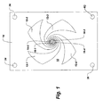
- Fig. 1 shows an antenna according to embodiments of the present invention, positioned on a printed circuit board
- Figs. 2-3 show aspects of the electrical connectivity of the antenna of Fig. 1 ;
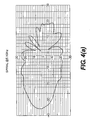
- Figs. 4(a)-4(b) are graphs showing the performance of the antenna of Fig. 1 at various frequencies;
- Figs. 5(a)-5(j) and 6(a) - 6(n) depict various packaging structures for the antenna of the present invention
- Fig. 7 depicts the operation of the present invention in a wireless KVM system.
- an antenna according to embodiments of the present invention as defined in claim 1, comprises a circularly polarized spiral antenna 10 formed by a metallic spiral pattern, e.g., on a substrate such as a printed circuit board (“PCB") 14 or the like.
- the spiral antenna 10 has four arms 12-1, 12-2, 12-3 and 12-4, each of which has a corresponding metallic contact area 16-1, 16-2, 16-3, 16 -4 near the center of the spiral.
- the arms are formed of a conductor (e.g., a metal) on the substrate 14.
- the substrate has four holes 18-1 , 18-2, 18-3, 18-4 therein, corresponding in location to be under the contact areas 16-1, 16-2, 16-3, 16 -4.
- the contact pins are either signal or ground pins.
- the holes are about 0.015 inches in diameter and are completely covered by their respective contact areas.
- Fig. 3 provides an enlarged view (for explanation purposes) of the contact pins and their connection to the various spiral arms.
- spiral arm 12-1 is electrically connected to signal pin 20
- spiral arm 12-2 is electrically connected to ground pins 22 and 24
- spiral arm 12-3 is electrically connected to ground pins 26 and 28
- spiral arm 12-4 is electrically connected to signal pin 30 .
- the gain of the antenna is preferably at least 6dBi and cover all the uni-bands of 802.11a, approximately 5.1 GHz to 5.9GHz.
- Figs. 4(a) and 4(b) show results of operating the antenna at 5.1 GHz and 5.9 GHz frequencies, respectively.
- the circularly polarized directional antenna has an average beam width of about 70 degrees making it fairly practical to use for long distance transmission.
- the antenna's bandwidth covers more than the bandwidth actually used, keeping a very linear plane rotation.
- the antenna achieves high radiant efficiency due to its low-loss compensating network designed as part of the antenna elements to have a frequency dependant linear rotation function.
- the four-arm spiral uses two low cost, independent, wideband matched power dividers for vertical and horizontal polarization directivity balancing.
- the two power dividers provide a choice of polarizations for a non-symmetric preformed beam width permitting the radios to select the best-fit polarization for transmitting and receiving data.
- each arm of the antenna planer structure is preferably two wavelengths (of the desired bandwidth).
- the wavelength center is optimized for best impedance match in the desired bandwidth.
- a finite ground plane is used to keep backward reflections and side lobes at minimum for best antenna efficiency and desired beam width angle.
- Figs. 4(a)-4(b) show plots of desired beam width for lower and upper uni-band frequencies
- the height of the ground plane to the bottom surface of the dielectric material under the conducting arms surfaces, and the center of the wavelength yield high antenna gain, beam angle, and antenna efficiency.
- the distance between the antenna and the ground plane is about 0.25 inches.
- This particular structure configuration also allows control of the beam angle by changing the height distance of the ground plane to the bottom surface of the dielectric material under the conducting arms surfaces with small effects on antenna efficiency and antenna matching due to its ultra broad band natural design topology.
- the spacing between the board and ground plane can be used to adjust the beam width (i.e., gain) and efficiency.
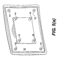
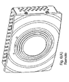
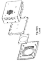
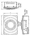
- spiral antenna of the present invention may be packaged in many ways. However, one packaging of the antenna is described herein with reference to Figs. 5(a)-5(j) .
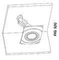
- Fig. 5(a) shows the back view of an antenna mount 32 , preferably formed of a light-weight molded plastic.
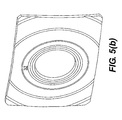
- Fig. 5(b) shows a front view of the antenna mount 32 .
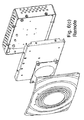
- the PCB (substrate) 14 has four holes 34, 36, 38, 40 in the four corners thereof. These holes allow the board to be positioned over four corresponding pins 42, 44, 46, 48 formed on a portion of the antenna mount 32..
- the PCB board 14 is mounted with the pins 42, 44, 46, 48 in the corresponding holes 34, 36, 38, 40 of the board such that the spiral antenna faces the front of the mount 32, and the connector and ground pins 20, 22, 24, 26, 28, 30, face the rear so that they may be connected with cables and or other circuitry.
- the back side of mount 32 has four pins 50, 52, 54, 56, one in each of the outer four corners thereof. These pins hold in place a rear cover 58 which may be secured to the mount 32 by four screws.
- the real cover 58 may house circuitry and provides connectors 60 , 62 to the antenna 10 housed on the mount 32 .
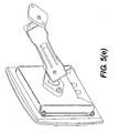
- the rear cover 58 has two holes 64 , 66 therein. Preferably these holes are threaded to enable connection of a ball joint 68 thereto, as shown in Fig. 5(d) .
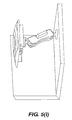
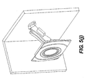
- the ball joint 68 may be connected to an arm 70 , itself having a ball joint 72 connected to another end thereof (as shown in Figs. 5(e)-5(g) .
- the entire construct housing the antenna may then be mounted on a wall, ceiling or other appropriate surface, as shown, e.g., in Figs. 5(h)-5(j) .
- the antenna may be positioned and aimed in a particular direction.
- the PCB 14 has dimensions 2..25 inches by 3.25 inches, and the holes 34, 36, 38, 40 are 0..156 inches in diameter, centered 0.200 inches from the edges of the board.
- This structure with its circular polarization for linear propagation used with an 802.11a communication link, allows minimal distortion, high efficiency and yields longer transmission distances.
- the structure uses two coax cables.
- Each coax cable is used for two functions: independent vertical and horizontal feeds; and as a 180 degree phase shifted broad band transformer to feed each arm of the antenna.
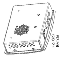
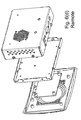
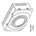
- FIG. 6(a)-6(k) Another packaging embodiment is shown in Figs. 6(a)-6(k) , where Figs. 6(a)-6(g) show the packaging of a remote-side unit, and Figs. 6(h) -b(n) show the packaging of a local-side unit.
- Fig. 7 depicts the use and operation of an antenna according to the present invention in a wireless KVM system.
- a target processor 74 is connected to a KVM wireless device 76 which is connected to a radio 78 .
- the radio has an antenna 10-1 connected thereto.
- a remote computer 82 is connected to a radio 80 which has an antenna 10-2 connected thereto. Either or both of the antennas 10-1 , 10-2 may be antennas according to embodiments of the present invention.
- the target processor 74 may be any type processor or collection of processors, including servers, processors in appliances such as ATM machines, kiosks and the like.
- the remote computer 82 connects via radio link 84 to the target processor 74 .
- the remote computer 82 may then access and / or control the target processor 74 , providing keyboard and mouse signals thereto and receiving keyboard, video and mouse signals therefrom.
- the target processor may not have a keyboard, mouse or display attached thereto (e.g., in the case of an embedded processor or a server or a processor in a device such as an ATM). In such cases, the processor would provide video signals to the remote computer 82 and receive KVM signals therefrom.
Abstract
Description
- This relates antennas, and, more specifically, to antennas for use in with KVM (Keyboard, Video, Mouse) systems.
- KVM systems enable one or mole remote computers to access and/or control one or more target computers. The term computer as used herein is nonlimiting and refers to any processor or collection of processors, including servers (and groups or racks thereof), processors in appliances such as ATM machines, kiosks, cash registers, set-top boxes, PCs and the like Early KVM systems used wired connections between the remote and target computers However, more recently, wireless KVM systems have become available, e.g., from Avocent Corporation, the assignee of the present application.
- A typical wireless KVM system connecting a target computer to a remote computer uses two radios, one at the target computer (or at a switch connected thereto) and the other at the remote computer. These systems preferably operate using the 802.11a standard Prior wireless KVM systems used two omnidirectional antennas. However, using this type of antenna limited the range of transmission between the two radios (the wireless transmitter and the wireless receiver) to about 100 feet through three walls and up to 300 feet line-of-sight. Notably, the distance range was limited by the antennas used, and not by issues relating to the 802.11a standard. It is desirable and an object of the present invention to extend the distance between the wireless radios (the Transmitter and the Receiver) in a KVM system, especially 802.11a-based wireless systems.
- This invention provides 802.11 a radios an efficient, circularly polarized directional antenna.
- It is a further object of the present invention that the transmitted and received signal modulation should not be distorted or sacrificed in group delay. Accordingly, a type of frequency independent structure that includes a match of 50 ohms across the operating bandwidth was developed and optimized.
-
US 6 130 652 A discloses an antenna apparatus comprising a spiral metallic pattern formed of four arms, each arm being connected to a central feed line and an end feed line. The pattern also includes four outer circumferential arms that are connected to ground via resistors. -
Fig. 1 shows an antenna according to embodiments of the present invention, positioned on a printed circuit board; -
Figs. 2-3 show aspects of the electrical connectivity of the antenna ofFig. 1 ; -
Figs. 4(a)-4(b) are graphs showing the performance of the antenna ofFig. 1 at various frequencies; -
Figs. 5(a)-5(j) and 6(a) - 6(n) depict various packaging structures for the antenna of the present invention; -
Fig. 7 depicts the operation of the present invention in a wireless KVM system. - With reference to
Fig. 1 , an antenna according to embodiments of the present invention as defined in claim 1, comprises a circularly polarizedspiral antenna 10 formed by a metallic spiral pattern, e.g., on a substrate such as a printed circuit board ("PCB") 14 or the like. Thespiral antenna 10 has four arms 12-1, 12-2, 12-3 and 12-4, each of which has a corresponding metallic contact area 16-1, 16-2, 16-3, 16 -4 near the center of the spiral. The arms are formed of a conductor (e.g., a metal) on thesubstrate 14. - In order to form electrical connections with the
antenna 10, when formed on asubstrate 14, as shown inFigs. 2-3 , the substrate has four holes 18-1, 18-2, 18-3, 18-4 therein, corresponding in location to be under the contact areas 16-1, 16-2, 16-3, 16 -4. Using wires passed through these holes, appropriate electrical contact may be made with each of the four antenna arms, through thesubstrate 14, to contact pins on the other side of the substrate. The contact pins are either signal or ground pins. In preferred embodiments the holes are about 0.015 inches in diameter and are completely covered by their respective contact areas. -
Fig. 3 provides an enlarged view (for explanation purposes) of the contact pins and their connection to the various spiral arms. In particular, in the embodiment shown, spiral arm 12-1 is electrically connected tosignal pin 20, spiral arm 12-2 is electrically connected toground pins ground pins signal pin 30. - The gain of the antenna is preferably at least 6dBi and cover all the uni-bands of 802.11a, approximately 5.1 GHz to 5.9GHz.
Figs. 4(a) and4(b) show results of operating the antenna at 5.1 GHz and 5.9 GHz frequencies, respectively. - In presently preferred embodiments of the invention, the circularly polarized directional antenna has an average beam width of about 70 degrees making it fairly practical to use for long distance transmission. The antenna's bandwidth covers more than the bandwidth actually used, keeping a very linear plane rotation. The antenna achieves high radiant efficiency due to its low-loss compensating network designed as part of the antenna elements to have a frequency dependant linear rotation function.
- The four-arm spiral uses two low cost, independent, wideband matched power dividers for vertical and horizontal polarization directivity balancing. The two power dividers provide a choice of polarizations for a non-symmetric preformed beam width permitting the radios to select the best-fit polarization for transmitting and receiving data.
- The conductor physical length of each arm of the antenna planer structure is preferably two wavelengths (of the desired bandwidth). The wavelength center is optimized for best impedance match in the desired bandwidth.
- In preferred embodiments, a finite ground plane is used to keep backward reflections and side lobes at minimum for best antenna efficiency and desired beam width angle.
Figs. 4(a)-4(b) show plots of desired beam width for lower and upper uni-band frequencies The height of the ground plane to the bottom surface of the dielectric material under the conducting arms surfaces, and the center of the wavelength yield high antenna gain, beam angle, and antenna efficiency. In presently preferred embodiments the distance between the antenna and the ground plane is about 0.25 inches. Other embodiments used spacing of up to about 0.5 inches. This particular structure configuration also allows control of the beam angle by changing the height distance of the ground plane to the bottom surface of the dielectric material under the conducting arms surfaces with small effects on antenna efficiency and antenna matching due to its ultra broad band natural design topology. In other words, the spacing between the board and ground plane can be used to adjust the beam width (i.e., gain) and efficiency. - One skilled in the art will realize that the spiral antenna of the present invention may be packaged in many ways. However, one packaging of the antenna is described herein with reference to
Figs. 5(a)-5(j) . -
Fig. 5(a) shows the back view of anantenna mount 32, preferably formed of a light-weight molded plastic.Fig. 5(b) shows a front view of theantenna mount 32. With reference toFig. 1 , in this embodiment the PCB (substrate) 14 has fourholes corresponding pins antenna mount 32.. ThePCB board 14 is mounted with thepins corresponding holes mount 32, and the connector andground pins - The back side of
mount 32 has fourpins rear cover 58 which may be secured to themount 32 by four screws. Thereal cover 58 may house circuitry and providesconnectors antenna 10 housed on themount 32. - The
rear cover 58 has twoholes ball joint 68 thereto, as shown inFig. 5(d) . Theball joint 68 may be connected to anarm 70, itself having aball joint 72 connected to another end thereof (as shown inFigs. 5(e)-5(g) . The entire construct housing the antenna may then be mounted on a wall, ceiling or other appropriate surface, as shown, e.g., inFigs. 5(h)-5(j) . One skilled in the art will realize that in this manner the antenna may be positioned and aimed in a particular direction. - In some preferred embodiments of the present invention, the PCB 14 has dimensions 2..25 inches by 3.25 inches, and the
holes - This structure, with its circular polarization for linear propagation used with an 802.11a communication link, allows minimal distortion, high efficiency and yields longer transmission distances.
- The structure uses two coax cables. Each coax cable is used for two functions: independent vertical and horizontal feeds; and as a 180 degree phase shifted broad band transformer to feed each arm of the antenna.
- Another packaging embodiment is shown in
Figs. 6(a)-6(k) , whereFigs. 6(a)-6(g) show the packaging of a remote-side unit, andFigs. 6(h) -b(n) show the packaging of a local-side unit. -
Fig. 7 depicts the use and operation of an antenna according to the present invention in a wireless KVM system.. Atarget processor 74 is connected to aKVM wireless device 76 which is connected to aradio 78. The radio has an antenna 10-1 connected thereto. Aremote computer 82 is connected to aradio 80 which has an antenna 10-2 connected thereto. Either or both of the antennas 10-1, 10-2 may be antennas according to embodiments of the present invention. As noted earlier, thetarget processor 74 may be any type processor or collection of processors, including servers, processors in appliances such as ATM machines, kiosks and the like. In operation, theremote computer 82 connects viaradio link 84 to thetarget processor 74. Theremote computer 82 may then access and / or control thetarget processor 74, providing keyboard and mouse signals thereto and receiving keyboard, video and mouse signals therefrom. In some cases the target processor may not have a keyboard, mouse or display attached thereto (e.g., in the case of an embedded processor or a server or a processor in a device such as an ATM). In such cases, the processor would provide video signals to theremote computer 82 and receive KVM signals therefrom.
Claims (9)
- An antenna apparatus comprising:a circuit board (14) mounted in a housing (32) constructed and adapted to direct the antenna in a specific direction,a spiral metallic pattern formed on a portion of the circuit board on a first side thereof, the spiral pattern being formed of four arms (12-1, 12-2, 12-3, 12-4), each arm having a contact location (16-1, 16-2, 16-3, 16 -4);characterized by
two signal connectors (20, 30) and four ground connectors (22, 24, 26, 28) being attached to a second side of said circuit board (14), wherein two of the arms (12-1, 12-4) are each electrically connected at the contact location to a respective signal connector (20, 30) and wherein a different two of the arms (12-2, 12-3) are each electrically connected at the contact location to two of the ground connectors (22, 24, 26, 28). - An antenna apparatus as in claim 1 wherein each arm (12-1, 12-2, 12-3, 12-4) has a contact location (16-1, 16-2, 16-3, 16 -4) near a center of the spiral.
- An antenna apparatus as in any of claims 1 to 2 further comprising a finite ground plane.
- An apparatus as in claim 3 wherein said finite ground plane is constructed and adapted to minimize backward reflections and side lobes.
- An apparatus as in any of claims 1-4 wherein:said two signal connectors (20, 30) are electrically connected to the ones of the spiral arms (12-1, 12-4) at the contact locations (16-1, 16 -4) thereof, said signal connectors being connected to said arms via holes (18-1, 18-2, 18-3, 18-4) in said circuit board.
- An apparatus as in claim 5 wherein each of said holes (18-1, 18-2, 18-3, 18-4) is substantially covered on said first side of said circuit board (14) by the contact location (16-1, 16-2, 16-3, 16 -4) of one of said four arms (12-1, 12-2, 12-3, 12-4).
- An apparatus as in any of claims 1-6 wherein the gain of the antenna is preferably at least 6dBi and covers the uni-bands of 802.11 a.
- An apparatus as in any of claims 1-7 wherein the apparatus forms a circularly polarized directional antenna with an average beam width of about 70 degrees.
- The apparatus any of claims 1-8 wherein a conductor physical length of each arm (12-1, 12-2, 12-3, 12-4) is preferably two wavelengths of a desired bandwidth.
Applications Claiming Priority (2)
| Application Number | Priority Date | Filing Date | Title |
|---|---|---|---|
| US10/948,307 US7075500B2 (en) | 2004-09-24 | 2004-09-24 | Antenna for wireless KVM, and housing therefor |
| PCT/US2005/034327 WO2006036855A1 (en) | 2004-09-24 | 2005-09-22 | Antenna for wireless kvm, and housing therefor |
Publications (3)
| Publication Number | Publication Date |
|---|---|
| EP1792364A1 EP1792364A1 (en) | 2007-06-06 |
| EP1792364A4 EP1792364A4 (en) | 2010-01-27 |
| EP1792364B1 true EP1792364B1 (en) | 2012-05-30 |
Family
ID=36098413
Family Applications (1)
| Application Number | Title | Priority Date | Filing Date |
|---|---|---|---|
| EP05800801A Not-in-force EP1792364B1 (en) | 2004-09-24 | 2005-09-22 | Spiral antenna |
Country Status (8)
| Country | Link |
|---|---|
| US (2) | US7075500B2 (en) |
| EP (1) | EP1792364B1 (en) |
| JP (1) | JP2008515288A (en) |
| CA (1) | CA2578213A1 (en) |
| IL (1) | IL182065A (en) |
| MY (1) | MY139275A (en) |
| TW (1) | TWI378600B (en) |
| WO (1) | WO2006036855A1 (en) |
Families Citing this family (8)
| Publication number | Priority date | Publication date | Assignee | Title |
|---|---|---|---|---|
| FR2925771B1 (en) * | 2007-12-21 | 2010-02-26 | Thales Sa | ANTENNAS NETWORK BROADBAND MULTI POLARIZATION INSTRUCTIONS |
| US7750868B1 (en) * | 2008-06-09 | 2010-07-06 | Scientific Applications & Research Associates, Inc | Low profile antenna for measuring the shielding effectiveness of hemp protected enclosures |
| TWI478440B (en) * | 2009-04-10 | 2015-03-21 | Chi Mei Comm Systems Inc | An uwb antenna and wireless communication device using the same |
| US20150173108A1 (en) * | 2013-12-13 | 2015-06-18 | Qualcomm Incorporated | Systems and methods for switching a set of wireless interactive devices |
| CN105896037B (en) * | 2016-06-01 | 2018-08-14 | 中国电子科技集团公司第五十四研究所 | A kind of coaxial feed spiral circle polarized omnidirectional antenna |
| US10552651B1 (en) * | 2016-06-29 | 2020-02-04 | United States Of America As Represented By The Administrator Of The National Aeronautics And Space | Frequency multiplexed radio frequency identification |
| US10944157B2 (en) | 2019-04-19 | 2021-03-09 | Bose Corporation | Multi-arm spiral antenna for a wireless device |
| US11525703B2 (en) | 2020-03-02 | 2022-12-13 | Bose Corporation | Integrated capacitor and antenna |
Family Cites Families (15)
| Publication number | Priority date | Publication date | Assignee | Title |
|---|---|---|---|---|
| US3562756A (en) * | 1968-06-03 | 1971-02-09 | Texas Instruments Inc | Multiple polarization spiral antenna |
| US3925784A (en) * | 1971-10-27 | 1975-12-09 | Radiation Inc | Antenna arrays of internally phased elements |
| JPH0296403A (en) * | 1988-10-03 | 1990-04-09 | Tech Res & Dev Inst Of Japan Def Agency | Antenna for wide band detector |
| US5453752A (en) * | 1991-05-03 | 1995-09-26 | Georgia Tech Research Corporation | Compact broadband microstrip antenna |
| US6166694A (en) * | 1998-07-09 | 2000-12-26 | Telefonaktiebolaget Lm Ericsson (Publ) | Printed twin spiral dual band antenna |
| US6130652A (en) * | 1999-06-15 | 2000-10-10 | Trw Inc. | Wideband, dual RHCP, LHCP single aperture direction finding antenna system |
| DE19929879A1 (en) * | 1999-06-29 | 2001-01-18 | Bosch Gmbh Robert | Spiral antenna |
| US6373446B2 (en) * | 2000-05-31 | 2002-04-16 | Bae Systems Information And Electronic Systems Integration Inc | Narrow-band, symmetric, crossed, circularly polarized meander line loaded antenna |
| JP2003188633A (en) | 2001-12-20 | 2003-07-04 | Mitsumi Electric Co Ltd | Combined antenna assembly |
| WO2003105273A2 (en) * | 2002-06-10 | 2003-12-18 | Hrl Laboratories, Llc | Low profile, dual polarized/pattern antenna |
| JP4103466B2 (en) * | 2002-06-27 | 2008-06-18 | 日立電線株式会社 | High-frequency connector surface mounting method, high-frequency connector mounting printed circuit board, and printed circuit board |
| JP3761501B2 (en) * | 2002-07-31 | 2006-03-29 | 本多通信工業株式会社 | Coaxial connector and ground pad on which it is mounted |
| US6765542B2 (en) * | 2002-09-23 | 2004-07-20 | Andrew Corporation | Multiband antenna |
| JP3558080B2 (en) * | 2003-01-20 | 2004-08-25 | 株式会社村田製作所 | Method of correcting measurement error, method of determining quality of electronic component, and electronic component characteristic measuring device |
| TWI349473B (en) * | 2003-07-11 | 2011-09-21 | Sk Telecom Co Ltd | Apparatus for reducing ground effects in a folder-type communications handset device |
-
2004
- 2004-09-24 US US10/948,307 patent/US7075500B2/en not_active Expired - Fee Related
-
2005
- 2005-09-21 TW TW094132624A patent/TWI378600B/en not_active IP Right Cessation
- 2005-09-22 WO PCT/US2005/034327 patent/WO2006036855A1/en active Application Filing
- 2005-09-22 JP JP2007533687A patent/JP2008515288A/en active Pending
- 2005-09-22 EP EP05800801A patent/EP1792364B1/en not_active Not-in-force
- 2005-09-22 CA CA002578213A patent/CA2578213A1/en not_active Abandoned
- 2005-09-23 MY MYPI20054506A patent/MY139275A/en unknown
-
2006
- 2006-05-09 US US11/429,950 patent/US7280085B2/en not_active Expired - Fee Related
-
2007
- 2007-03-20 IL IL182065A patent/IL182065A/en not_active IP Right Cessation
Also Published As
| Publication number | Publication date |
|---|---|
| MY139275A (en) | 2009-09-30 |
| JP2008515288A (en) | 2008-05-08 |
| US20060202908A1 (en) | 2006-09-14 |
| CA2578213A1 (en) | 2006-04-06 |
| IL182065A (en) | 2012-10-31 |
| EP1792364A4 (en) | 2010-01-27 |
| EP1792364A1 (en) | 2007-06-06 |
| US7075500B2 (en) | 2006-07-11 |
| TWI378600B (en) | 2012-12-01 |
| TW200623521A (en) | 2006-07-01 |
| IL182065A0 (en) | 2007-07-24 |
| US20060066500A1 (en) | 2006-03-30 |
| US7280085B2 (en) | 2007-10-09 |
| WO2006036855A1 (en) | 2006-04-06 |
Similar Documents
| Publication | Publication Date | Title |
|---|---|---|
| EP1792364B1 (en) | Spiral antenna | |
| JP6854326B2 (en) | Electronic device with communication and ranging functions | |
| US9407012B2 (en) | Antenna with dual polarization and mountable antenna elements | |
| CN206076482U (en) | Electronic equipment | |
| CN112563728B (en) | Millimeter wave antenna with continuously stacked radiating elements | |
| US6366258B2 (en) | Low profile high polarization purity dual-polarized antennas | |
| US6531985B1 (en) | Integrated laptop antenna using two or more antennas | |
| US6337666B1 (en) | Planar sleeve dipole antenna | |
| US6339404B1 (en) | Diversity antenna system for lan communication system | |
| US7215296B2 (en) | Switched multi-beam antenna | |
| US9401545B2 (en) | Multi polarization conformal channel monopole antenna | |
| US6208311B1 (en) | Dipole antenna for use in wireless communications system | |
| US8223077B2 (en) | Multisector parallel plate antenna for electronic devices | |
| JP2005210521A (en) | Antenna device | |
| JP6661714B2 (en) | Microwave equipment | |
| WO2021083223A1 (en) | Antenna unit and electronic device | |
| CN110828985A (en) | Antenna unit and electronic equipment | |
| TWI600209B (en) | Antenna reset circuit | |
| WO2021083218A1 (en) | Antenna unit and electronic device | |
| JP3006399B2 (en) | Dual band antenna | |
| CN102751569A (en) | Low-cost broadband vertical polarization ultra high frequency (UHF) wave band antenna installed in limited space | |
| US6690924B1 (en) | Circular polarization antenna for wireless communications | |
| US20100123637A1 (en) | Antenna | |
| JP2022148624A (en) | antenna device |
Legal Events
| Date | Code | Title | Description |
|---|---|---|---|
| PUAI | Public reference made under article 153(3) epc to a published international application that has entered the european phase |
Free format text: ORIGINAL CODE: 0009012 |
|
| 17P | Request for examination filed |
Effective date: 20070405 |
|
| AK | Designated contracting states |
Kind code of ref document: A1 Designated state(s): BE DE GB LU NL |
|
| DAX | Request for extension of the european patent (deleted) | ||
| RBV | Designated contracting states (corrected) |
Designated state(s): BE DE GB LU NL |
|
| A4 | Supplementary search report drawn up and despatched |
Effective date: 20091228 |
|
| RIC1 | Information provided on ipc code assigned before grant |
Ipc: H01Q 1/36 20060101ALI20091218BHEP Ipc: H01Q 1/42 20060101ALI20091218BHEP Ipc: H01Q 9/27 20060101AFI20091218BHEP Ipc: H01Q 21/24 20060101ALI20091218BHEP Ipc: H01Q 1/38 20060101ALI20091218BHEP Ipc: H01Q 1/12 20060101ALI20091218BHEP |
|
| 17Q | First examination report despatched |
Effective date: 20100412 |
|
| REG | Reference to a national code |
Ref country code: DE Ref legal event code: R079 Ref document number: 602005034452 Country of ref document: DE Free format text: PREVIOUS MAIN CLASS: H01Q0001360000 Ipc: H01Q0009270000 |
|
| GRAP | Despatch of communication of intention to grant a patent |
Free format text: ORIGINAL CODE: EPIDOSNIGR1 |
|
| RIC1 | Information provided on ipc code assigned before grant |
Ipc: H01Q 1/42 20060101ALI20111123BHEP Ipc: H01Q 21/24 20060101ALI20111123BHEP Ipc: H01Q 1/12 20060101ALI20111123BHEP Ipc: H01Q 1/38 20060101ALI20111123BHEP Ipc: H01Q 9/27 20060101AFI20111123BHEP Ipc: H01Q 1/36 20060101ALI20111123BHEP |
|
| RTI1 | Title (correction) |
Free format text: SPIRAL ANTENNA |
|
| GRAS | Grant fee paid |
Free format text: ORIGINAL CODE: EPIDOSNIGR3 |
|
| GRAA | (expected) grant |
Free format text: ORIGINAL CODE: 0009210 |
|
| AK | Designated contracting states |
Kind code of ref document: B1 Designated state(s): BE DE GB LU NL |
|
| REG | Reference to a national code |
Ref country code: GB Ref legal event code: FG4D |
|
| REG | Reference to a national code |
Ref country code: DE Ref legal event code: R096 Ref document number: 602005034452 Country of ref document: DE Effective date: 20120802 |
|
| REG | Reference to a national code |
Ref country code: NL Ref legal event code: VDEP Effective date: 20120530 |
|
| PG25 | Lapsed in a contracting state [announced via postgrant information from national office to epo] |
Ref country code: BE Free format text: LAPSE BECAUSE OF FAILURE TO SUBMIT A TRANSLATION OF THE DESCRIPTION OR TO PAY THE FEE WITHIN THE PRESCRIBED TIME-LIMIT Effective date: 20120530 |
|
| PG25 | Lapsed in a contracting state [announced via postgrant information from national office to epo] |
Ref country code: NL Free format text: LAPSE BECAUSE OF FAILURE TO SUBMIT A TRANSLATION OF THE DESCRIPTION OR TO PAY THE FEE WITHIN THE PRESCRIBED TIME-LIMIT Effective date: 20120530 |
|
| REG | Reference to a national code |
Ref country code: DE Ref legal event code: R119 Ref document number: 602005034452 Country of ref document: DE |
|
| PLBE | No opposition filed within time limit |
Free format text: ORIGINAL CODE: 0009261 |
|
| STAA | Information on the status of an ep patent application or granted ep patent |
Free format text: STATUS: NO OPPOSITION FILED WITHIN TIME LIMIT |
|
| 26N | No opposition filed |
Effective date: 20130301 |
|
| GBPC | Gb: european patent ceased through non-payment of renewal fee |
Effective date: 20120922 |
|
| REG | Reference to a national code |
Ref country code: DE Ref legal event code: R097 Ref document number: 602005034452 Country of ref document: DE Effective date: 20130301 |
|
| PG25 | Lapsed in a contracting state [announced via postgrant information from national office to epo] |
Ref country code: GB Free format text: LAPSE BECAUSE OF NON-PAYMENT OF DUE FEES Effective date: 20120922 Ref country code: DE Free format text: LAPSE BECAUSE OF NON-PAYMENT OF DUE FEES Effective date: 20130403 |
|
| REG | Reference to a national code |
Ref country code: DE Ref legal event code: R119 Ref document number: 602005034452 Country of ref document: DE Effective date: 20130403 |
|
| PG25 | Lapsed in a contracting state [announced via postgrant information from national office to epo] |
Ref country code: LU Free format text: LAPSE BECAUSE OF NON-PAYMENT OF DUE FEES Effective date: 20120922 |