EP1791074A1 - Belichtungseinstellung in einem Maschinenvisionssystem - Google Patents
Belichtungseinstellung in einem Maschinenvisionssystem Download PDFInfo
- Publication number
- EP1791074A1 EP1791074A1 EP05270087A EP05270087A EP1791074A1 EP 1791074 A1 EP1791074 A1 EP 1791074A1 EP 05270087 A EP05270087 A EP 05270087A EP 05270087 A EP05270087 A EP 05270087A EP 1791074 A1 EP1791074 A1 EP 1791074A1
- Authority
- EP
- European Patent Office
- Prior art keywords
- zone
- image
- frame
- exposure time
- zones
- Prior art date
- Legal status (The legal status is an assumption and is not a legal conclusion. Google has not performed a legal analysis and makes no representation as to the accuracy of the status listed.)
- Granted
Links
- 239000007787 solid Substances 0.000 claims abstract description 8
- 238000005096 rolling process Methods 0.000 claims abstract description 4
- 238000000034 method Methods 0.000 claims description 13
- 230000001934 delay Effects 0.000 claims description 2
- 238000005286 illumination Methods 0.000 description 3
- 230000001960 triggered effect Effects 0.000 description 2
- 238000003384 imaging method Methods 0.000 description 1
- 238000012986 modification Methods 0.000 description 1
- 230000004048 modification Effects 0.000 description 1
Images
Classifications
-
- G—PHYSICS
- G06—COMPUTING; CALCULATING OR COUNTING
- G06K—GRAPHICAL DATA READING; PRESENTATION OF DATA; RECORD CARRIERS; HANDLING RECORD CARRIERS
- G06K7/00—Methods or arrangements for sensing record carriers, e.g. for reading patterns
- G06K7/10—Methods or arrangements for sensing record carriers, e.g. for reading patterns by electromagnetic radiation, e.g. optical sensing; by corpuscular radiation
- G06K7/10544—Methods or arrangements for sensing record carriers, e.g. for reading patterns by electromagnetic radiation, e.g. optical sensing; by corpuscular radiation by scanning of the records by radiation in the optical part of the electromagnetic spectrum
- G06K7/10712—Fixed beam scanning
- G06K7/10722—Photodetector array or CCD scanning
-
- H—ELECTRICITY
- H04—ELECTRIC COMMUNICATION TECHNIQUE
- H04N—PICTORIAL COMMUNICATION, e.g. TELEVISION
- H04N25/00—Circuitry of solid-state image sensors [SSIS]; Control thereof
- H04N25/50—Control of the SSIS exposure
- H04N25/57—Control of the dynamic range
- H04N25/58—Control of the dynamic range involving two or more exposures
- H04N25/581—Control of the dynamic range involving two or more exposures acquired simultaneously
- H04N25/583—Control of the dynamic range involving two or more exposures acquired simultaneously with different integration times
-
- G—PHYSICS
- G06—COMPUTING; CALCULATING OR COUNTING
- G06K—GRAPHICAL DATA READING; PRESENTATION OF DATA; RECORD CARRIERS; HANDLING RECORD CARRIERS
- G06K7/00—Methods or arrangements for sensing record carriers, e.g. for reading patterns
- G06K7/10—Methods or arrangements for sensing record carriers, e.g. for reading patterns by electromagnetic radiation, e.g. optical sensing; by corpuscular radiation
- G06K7/10544—Methods or arrangements for sensing record carriers, e.g. for reading patterns by electromagnetic radiation, e.g. optical sensing; by corpuscular radiation by scanning of the records by radiation in the optical part of the electromagnetic spectrum
- G06K7/10712—Fixed beam scanning
- G06K7/10722—Photodetector array or CCD scanning
- G06K7/10752—Exposure time control
-
- H—ELECTRICITY
- H04—ELECTRIC COMMUNICATION TECHNIQUE
- H04N—PICTORIAL COMMUNICATION, e.g. TELEVISION
- H04N25/00—Circuitry of solid-state image sensors [SSIS]; Control thereof
- H04N25/50—Control of the SSIS exposure
- H04N25/53—Control of the integration time
- H04N25/531—Control of the integration time by controlling rolling shutters in CMOS SSIS
Definitions
- This invention the automatic setting of exposure levels in machine vision systems.
- the invention is particularly, but not exclusively, applicable to systems and devices for reading bar codes.
- the reader will be placed in a standby mode when not actively reading. When a reading is then taken, it is necessary to set the exposure level in accordance with ambient conditions; in prior art systems this is commonly done by taking a significant number (typically about 20) of frames of differing exposures and then selecting the best exposure for the ambient conditions. However, this number of frames leads to unnecessary power consumption and can cause problems owing to movement of the reader during the process.
- roaming devices are used in greatly differing ambient conditions which may range from direct sunlight to very low illumination levels within warehouses.
- Many designs have a default configuration in which the target is illuminated by LEDs, which are power hungry. It would be desirable to disable the LEDs as quickly as possible where ambient illumination is sufficient to permit this.
- the present invention provides a method of setting exposure level in a solid state image sensing system, the method comprising:
- Said zones preferably comprise successive groups of rows of pixels, and the respective exposure times for the zones are set by using a rolling blade system with different time delays between reset and readout.
- the readout from each zone may be processed to give a statistical value of the image sensed in the zone, said processing preferably being carried out on the same chip as the image sensor.
- Said best exposure time may be determined as the zone exposure time which produces the most acceptable image quality.
- said best exposure time may be determined by interpolation between zone exposure times.
- the image sensed is a digital pattern image, more preferably a bar code.
- the present invention provides a solid state image sensing device comprising an array of pixels, reset means for resetting said pixels, readout means for reading out pixel integrated light values, and control means for producing a time delay between reset and readout of the pixels which varies between predetermined zones of said array.
- the device preferably includes processing means on the same chip arranged to produce zone statistics from the readout pixel values of each zone.
- the invention provides apparatus for reading a digital pattern, comprising a solid state image sensing device as defined above, and a lens system for forming an image of said digital pattern on the pixel array, typically in the form of a handheld mobile device for reading bar codes.
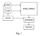
- a solid state image sensor 10 used in a bar code reader comprises a pixel array 12.
- the pixel array 12 is a CMOS array of 3-transistor or 4-transistor type, as is well known. In principle, the invention could also be applied to other types of pixel array, such as a CCD sensor.
- the image sensor 12 also comprises a reset circuit 14 and a read circuit 16 controlled by a control circuit 18.
- the control circuit 18 is operable to control the line spacing between read and reset so as to control exposure time in a "rolling blade" manner.
- the exposure time can be varied within each frame to divide the frame into a number of zones of varying exposure time.
- the zones are of progressively increasing exposure time.
- the statistics for each zone of the search frame are then used to select an exposure setting for the subsequent frame, or 'captured' frame. This may be done by selecting the zone is the search frame which produced the best result in the search frame, and using the same exposure time in the capture frame. Alternatively, the exposure time for the capture frame may be chosen by interpolating between the two best zones in the search frame. This processing can conveniently be carried out during the normal interframe time.
- the selected exposure time is then used during the whole of the captured frame.
- the same processing circuit may be used to process the pixel readout to decode the bar code.
- the sensor then reverts to a sleep mode until next triggered.
- the senor of the invention is capable of reading bar codes in only two frames, considerably reducing power consumption both in the imaging sensing circuitry itself and also in any associated illumination means.
- processing circuitry could be embodied on a separate chip, although a single chip embodiment is preferred.
- the invention is also potentially useful with other forms of image sensor.
Priority Applications (3)
| Application Number | Priority Date | Filing Date | Title |
|---|---|---|---|
| DE602005013404T DE602005013404D1 (de) | 2005-11-28 | 2005-11-28 | Belichtungseinstellung in einem Maschinenvisionssystem |
| EP05270087A EP1791074B1 (de) | 2005-11-28 | 2005-11-28 | Belichtungseinstellung in einem Maschinenvisionssystem |
| US11/559,113 US8477222B2 (en) | 2005-11-28 | 2006-11-13 | Method and apparatus for exposure level setting in machine vision systems |
Applications Claiming Priority (1)
| Application Number | Priority Date | Filing Date | Title |
|---|---|---|---|
| EP05270087A EP1791074B1 (de) | 2005-11-28 | 2005-11-28 | Belichtungseinstellung in einem Maschinenvisionssystem |
Publications (2)
| Publication Number | Publication Date |
|---|---|
| EP1791074A1 true EP1791074A1 (de) | 2007-05-30 |
| EP1791074B1 EP1791074B1 (de) | 2009-03-18 |
Family
ID=35945167
Family Applications (1)
| Application Number | Title | Priority Date | Filing Date |
|---|---|---|---|
| EP05270087A Active EP1791074B1 (de) | 2005-11-28 | 2005-11-28 | Belichtungseinstellung in einem Maschinenvisionssystem |
Country Status (3)
| Country | Link |
|---|---|
| US (1) | US8477222B2 (de) |
| EP (1) | EP1791074B1 (de) |
| DE (1) | DE602005013404D1 (de) |
Cited By (2)
| Publication number | Priority date | Publication date | Assignee | Title |
|---|---|---|---|---|
| EP3324329A1 (de) * | 2016-11-16 | 2018-05-23 | Hand Held Products, Inc. | Leser für unter zwei oder mehreren abbildungsbedingungen dargestellte optische zeichen innerhalb einer einzigen rahmenzeit |
| WO2019042890A1 (fr) | 2017-09-01 | 2019-03-07 | Teledyne E2V Semiconductors Sas | Procede d'acquisition d'image par un capteur d'image de type cmos pour la reconnaissance de code lisible optiquement |
Families Citing this family (1)
| Publication number | Priority date | Publication date | Assignee | Title |
|---|---|---|---|---|
| US8780241B2 (en) * | 2011-01-25 | 2014-07-15 | Aptina Imaging Corporation | Digitally graded neutral density filter |
Citations (3)
| Publication number | Priority date | Publication date | Assignee | Title |
|---|---|---|---|---|
| US5646390A (en) * | 1994-07-26 | 1997-07-08 | Metanetics Corporation | Dataform readers and methods |
| US5815200A (en) * | 1994-07-26 | 1998-09-29 | Metanetics Corporation | Extended working range dataform reader with reduced power consumption |
| US20020039137A1 (en) * | 2000-09-30 | 2002-04-04 | Harper Jeffrey D. | Methods and apparatus for automatic exposure control |
Family Cites Families (4)
| Publication number | Priority date | Publication date | Assignee | Title |
|---|---|---|---|---|
| US5745808A (en) * | 1995-08-21 | 1998-04-28 | Eastman Kodak Company | Camera exposure control system using variable-length exposure tables |
| ATE506807T1 (de) * | 2001-06-18 | 2011-05-15 | Casio Computer Co Ltd | Photosensorsystem und ansteuerungsverfahren dafür |
| WO2003083773A2 (en) * | 2002-03-27 | 2003-10-09 | The Trustees Of Columbia University In The City Of New York | Imaging method and system |
| US7978245B2 (en) * | 2004-06-24 | 2011-07-12 | Hewlett-Packard Development Company, L.P. | Method and apparatus for controlling color balance in a digital imaging device |
-
2005
- 2005-11-28 EP EP05270087A patent/EP1791074B1/de active Active
- 2005-11-28 DE DE602005013404T patent/DE602005013404D1/de active Active
-
2006
- 2006-11-13 US US11/559,113 patent/US8477222B2/en active Active
Patent Citations (3)
| Publication number | Priority date | Publication date | Assignee | Title |
|---|---|---|---|---|
| US5646390A (en) * | 1994-07-26 | 1997-07-08 | Metanetics Corporation | Dataform readers and methods |
| US5815200A (en) * | 1994-07-26 | 1998-09-29 | Metanetics Corporation | Extended working range dataform reader with reduced power consumption |
| US20020039137A1 (en) * | 2000-09-30 | 2002-04-04 | Harper Jeffrey D. | Methods and apparatus for automatic exposure control |
Cited By (7)
| Publication number | Priority date | Publication date | Assignee | Title |
|---|---|---|---|---|
| EP3324329A1 (de) * | 2016-11-16 | 2018-05-23 | Hand Held Products, Inc. | Leser für unter zwei oder mehreren abbildungsbedingungen dargestellte optische zeichen innerhalb einer einzigen rahmenzeit |
| US10114997B2 (en) | 2016-11-16 | 2018-10-30 | Hand Held Products, Inc. | Reader for optical indicia presented under two or more imaging conditions within a single frame time |
| US10311274B2 (en) | 2016-11-16 | 2019-06-04 | Hand Held Products, Inc. | Reader for optical indicia presented under two or more imaging conditions within a single frame time |
| WO2019042890A1 (fr) | 2017-09-01 | 2019-03-07 | Teledyne E2V Semiconductors Sas | Procede d'acquisition d'image par un capteur d'image de type cmos pour la reconnaissance de code lisible optiquement |
| FR3070779A1 (fr) * | 2017-09-01 | 2019-03-08 | Teledyne E2V Semiconductors Sas | Procede d'acquisition d'image par un capteur d'image de type cmos pour la reconnaissance de code lisible optiquement |
| JP2020532249A (ja) * | 2017-09-01 | 2020-11-05 | テレダイン・イー・2・ブイ・セミコンダクターズ・エス・ア・エス | 光学的に読み取り可能なコードを認識するcmos型画像センサによる画像取得方法 |
| US10896303B2 (en) | 2017-09-01 | 2021-01-19 | Teledyne E2V Semiconductors Sas | Method of image acquisition by an image sensor of CMOS type for the recognition of optically readable code |
Also Published As
| Publication number | Publication date |
|---|---|
| DE602005013404D1 (de) | 2009-04-30 |
| US8477222B2 (en) | 2013-07-02 |
| US20070126922A1 (en) | 2007-06-07 |
| EP1791074B1 (de) | 2009-03-18 |
Similar Documents
| Publication | Publication Date | Title |
|---|---|---|
| US9609241B2 (en) | Image sensor pixel array having output response curve including logarithmic pattern for image sensor based terminal | |
| EP2410463A1 (de) | Endgerät zur Ausgabe von monochromen Bilddaten und Farbbilddaten | |
| US9129172B2 (en) | Indicia reading terminal with color frame processing | |
| US8910875B2 (en) | Indicia reading terminal with color frame processing | |
| US8083146B2 (en) | Optical code reading system and method for processing multiple resolution representations of an image | |
| EP2284766B1 (de) | Markierungsleser mit unterschiedlichen Belichtungszeiten | |
| US9438868B2 (en) | Adaptive image sensor systems and methods | |
| JP5592643B2 (ja) | フレーム処理を含む証印読取端末 | |
| US20110080500A1 (en) | Imaging terminal, imaging sensor having multiple reset and/or multiple read mode and methods for operating the same | |
| EP1453304B1 (de) | Bildsensor mit doppelter automatischer Belichtungssteuerung | |
| US9030583B2 (en) | Imaging system with foveated imaging capabilites | |
| US20070263109A1 (en) | Imager integrated CMOS circuit chip and associated optical code reading systems | |
| CN101860689A (zh) | 固体摄像器件、固体摄像器件的信号处理方法及电子装置 | |
| EP3394791B1 (de) | Lesegerät für codierte informationen | |
| WO2002063543A2 (en) | Optical reader having partial frame operating mode | |
| EP1791074B1 (de) | Belichtungseinstellung in einem Maschinenvisionssystem | |
| US11823005B2 (en) | Optical reading device | |
| JP7410675B2 (ja) | 撮像装置及びその制御方法 | |
| EP2562680B1 (de) | Optisches Codelesegerät mit einem Farbbildsensor | |
| US9491380B2 (en) | Methods for triggering for multi-camera system | |
| JP2006235719A (ja) | 撮像方法及び撮像装置 | |
| WO2010014084A1 (en) | One dimensional barcode reader using two dimensional image sensor | |
| US6942152B1 (en) | Versatile graphical code reader that is configured for efficient decoding | |
| US20080266444A1 (en) | Method, apparatus, and system for continuous autofocusing | |
| EP3844945B1 (de) | Verfahren und vorrichtung zur dynamischen bilderfassung basierend auf bewegungsinformation in einem bild |
Legal Events
| Date | Code | Title | Description |
|---|---|---|---|
| PUAI | Public reference made under article 153(3) epc to a published international application that has entered the european phase |
Free format text: ORIGINAL CODE: 0009012 |
|
| AK | Designated contracting states |
Kind code of ref document: A1 Designated state(s): AT BE BG CH CY CZ DE DK EE ES FI FR GB GR HU IE IS IT LI LT LU LV MC NL PL PT RO SE SI SK TR |
|
| AX | Request for extension of the european patent |
Extension state: AL BA HR MK YU |
|
| 17P | Request for examination filed |
Effective date: 20071102 |
|
| 17Q | First examination report despatched |
Effective date: 20071213 |
|
| AKX | Designation fees paid |
Designated state(s): DE FR GB IT |
|
| GRAP | Despatch of communication of intention to grant a patent |
Free format text: ORIGINAL CODE: EPIDOSNIGR1 |
|
| GRAS | Grant fee paid |
Free format text: ORIGINAL CODE: EPIDOSNIGR3 |
|
| GRAA | (expected) grant |
Free format text: ORIGINAL CODE: 0009210 |
|
| AK | Designated contracting states |
Kind code of ref document: B1 Designated state(s): DE FR GB IT |
|
| REG | Reference to a national code |
Ref country code: GB Ref legal event code: FG4D |
|
| REF | Corresponds to: |
Ref document number: 602005013404 Country of ref document: DE Date of ref document: 20090430 Kind code of ref document: P |
|
| PLBE | No opposition filed within time limit |
Free format text: ORIGINAL CODE: 0009261 |
|
| STAA | Information on the status of an ep patent application or granted ep patent |
Free format text: STATUS: NO OPPOSITION FILED WITHIN TIME LIMIT |
|
| 26N | No opposition filed |
Effective date: 20091221 |
|
| REG | Reference to a national code |
Ref country code: FR Ref legal event code: ST Effective date: 20100730 |
|
| PG25 | Lapsed in a contracting state [announced via postgrant information from national office to epo] |
Ref country code: FR Free format text: LAPSE BECAUSE OF NON-PAYMENT OF DUE FEES Effective date: 20091130 |
|
| PG25 | Lapsed in a contracting state [announced via postgrant information from national office to epo] |
Ref country code: IT Free format text: LAPSE BECAUSE OF FAILURE TO SUBMIT A TRANSLATION OF THE DESCRIPTION OR TO PAY THE FEE WITHIN THE PRESCRIBED TIME-LIMIT Effective date: 20090318 |
|
| PGFP | Annual fee paid to national office [announced via postgrant information from national office to epo] |
Ref country code: GB Payment date: 20121025 Year of fee payment: 8 |
|
| GBPC | Gb: european patent ceased through non-payment of renewal fee |
Effective date: 20131128 |
|
| PG25 | Lapsed in a contracting state [announced via postgrant information from national office to epo] |
Ref country code: GB Free format text: LAPSE BECAUSE OF NON-PAYMENT OF DUE FEES Effective date: 20131128 |
|
| PGFP | Annual fee paid to national office [announced via postgrant information from national office to epo] |
Ref country code: DE Payment date: 20231019 Year of fee payment: 19 |