EP1790978B1 - Temperature compensated vapor sensor - Google Patents
Temperature compensated vapor sensor Download PDFInfo
- Publication number
- EP1790978B1 EP1790978B1 EP06024012A EP06024012A EP1790978B1 EP 1790978 B1 EP1790978 B1 EP 1790978B1 EP 06024012 A EP06024012 A EP 06024012A EP 06024012 A EP06024012 A EP 06024012A EP 1790978 B1 EP1790978 B1 EP 1790978B1
- Authority
- EP
- European Patent Office
- Prior art keywords
- resistor
- switch
- resistance
- sensing element
- circuit
- Prior art date
- Legal status (The legal status is an assumption and is not a legal conclusion. Google has not performed a legal analysis and makes no representation as to the accuracy of the status listed.)
- Not-in-force
Links
Images
Classifications
-
- G—PHYSICS
- G01—MEASURING; TESTING
- G01N—INVESTIGATING OR ANALYSING MATERIALS BY DETERMINING THEIR CHEMICAL OR PHYSICAL PROPERTIES
- G01N27/00—Investigating or analysing materials by the use of electric, electrochemical, or magnetic means
- G01N27/02—Investigating or analysing materials by the use of electric, electrochemical, or magnetic means by investigating impedance
- G01N27/04—Investigating or analysing materials by the use of electric, electrochemical, or magnetic means by investigating impedance by investigating resistance
- G01N27/12—Investigating or analysing materials by the use of electric, electrochemical, or magnetic means by investigating impedance by investigating resistance of a solid body in dependence upon absorption of a fluid; of a solid body in dependence upon reaction with a fluid, for detecting components in the fluid
- G01N27/122—Circuits particularly adapted therefor, e.g. linearising circuits
-
- G—PHYSICS
- G01—MEASURING; TESTING
- G01N—INVESTIGATING OR ANALYSING MATERIALS BY DETERMINING THEIR CHEMICAL OR PHYSICAL PROPERTIES
- G01N33/00—Investigating or analysing materials by specific methods not covered by groups G01N1/00 - G01N31/00
- G01N33/0004—Gaseous mixtures, e.g. polluted air
- G01N33/0009—General constructional details of gas analysers, e.g. portable test equipment
- G01N33/0027—General constructional details of gas analysers, e.g. portable test equipment concerning the detector
- G01N33/0031—General constructional details of gas analysers, e.g. portable test equipment concerning the detector comprising two or more sensors, e.g. a sensor array
-
- G—PHYSICS
- G01—MEASURING; TESTING
- G01N—INVESTIGATING OR ANALYSING MATERIALS BY DETERMINING THEIR CHEMICAL OR PHYSICAL PROPERTIES
- G01N33/00—Investigating or analysing materials by specific methods not covered by groups G01N1/00 - G01N31/00
- G01N33/0004—Gaseous mixtures, e.g. polluted air
- G01N33/0009—General constructional details of gas analysers, e.g. portable test equipment
- G01N33/0062—General constructional details of gas analysers, e.g. portable test equipment concerning the measuring method or the display, e.g. intermittent measurement or digital display
- G01N33/0063—General constructional details of gas analysers, e.g. portable test equipment concerning the measuring method or the display, e.g. intermittent measurement or digital display using a threshold to release an alarm or displaying means
Definitions
- the present invention relates to chemiresistor sensors.
- the present invention relates to a chemiresistor sensor system having multiple resistive elements that can be selectively incorporated into a sensor circuit to change the overall resistance of the circuit in response to changes in ambient temperature.
- Detecting the presence of specific chemical compounds in the atmosphere is important in a variety of different applications. For example, it is often important to detect the presence and concentration of potentially flammable compounds in the atmosphere. Chemical compounds of interest are often referred to as target analytes.
- a variety of different sensor systems known in the art can be used to detect the presence and concentration of different analytes.
- conductiometric sensor systems for example, conductiometric sensor systems, optical sensor systems, and surface acoustic wave sensor systems can all be used.
- Polymer-absorption chemiresistor sensors include a sensor probe having a pair of electrodes and a sensing element. The probe is part of a sensor circuit.
- the sensing element typically takes the form of a polymeric sensor film that spans the two electrodes.
- the sensor film is exposed to the surrounding atmosphere.
- the exact composition of the polymeric sensor film varies depending on the target analyte, as is known in the art, such that the sensor film absorbs the target analyte when it is present in the surrounding atmosphere.
- a load is applied across the sensor film via the electrodes.
- the sensor film swells and undergoes a volumetric change. The change in volume changes the electrical resistance of the film.
- a processor or control unit is typically coupled to the sensor circuit.
- the processor monitors the resistance of the sensor film to determine the absence, presence, and concentration of the target analytes.
- the processor can be coupled to a user interface.
- the user interface typically includes an indicating device that generates a signal when the concentration of the target analyte exceeds a predetermined threshold value.
- the resistance of the sensor film changes not only in response to absorption of the target analytes, but also in response to changes in ambient temperature. If the sensor film has a positive temperature coefficient of resistance, the resistance of the sensor film increases as ambient temperature increases. If the sensor film has a negative temperature coefficient of resistance, the resistance of the sensor film decreases as ambient temperature increases. Whether the sensor film has a positive or negative temperature coefficient of resistance depends on the composition of the sensor film and the application.
- detection of target analytes is based on changes in the resistance of the sensor film that occur when the sensor absorbs target analytes
- changes in ambient temperature that change the resistance of the sensor film can negatively affect the sensor system's ability to accurately detect the presence of target analytes. For example, if the sensor film has a positive temperature coefficient of resistance and increases in resistance upon the absorption of target analytes, increases in ambient temperature might cause the sensor system to generate a false signal indicating that target analytes are present when they are not.
- chemiresistor sensor systems While conventional chemiresistor sensor systems perform adequately for their intended uses, they are subject to improvement. Specifically, there is a need for a chemiresistor sensor system that can modify its overall resistance in response to changes in ambient temperature to increase the accuracy of the sensor system.
- the sensor system improves upon the prior art by providing a chemiresistor sensor system that compensates for changes in resistance caused by changes in ambient temperature, thereby increasing the accuracy of the sensor system's ability to detect target analytes.
- the sensor system generally includes a first resistor, a second resistor, and a load regulator or switch. At least one of the first resistor and the second resistor is a sensing element having a resistance that changes in response to the presence of one or more of the analytes. The resistors also change resistance in response to changes in ambient temperature.
- the switch manages an electrical load across the first resistor and the second resistor.
- the switch prevents passage of the electrical load across the first and/or second resistor(s) when the ambient temperature is at a first value.
- the switch permits passage of the electrical load across the first and/or second resistor when the ambient temperature is at a second value.
- the sensor system advantageously incorporates the first and/or second resistors into a sensing circuit in response to changes in ambient temperature.
- the sensor system is able to change its overall resistance to compensate for changes in resistance of the first and second resistors caused by changes in ambient temperature.
- the sensor system's ability to compensate for changes in resistance caused by changes in ambient temperature increases the system's ability to accurately detect the presence of target analytes.
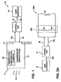
- Figure 1 generally depicts the major components of an exemplary chemiresistor sensor system at 10.
- the sensor system 10 is generally comprised of a chemiresistor sensor probe 12, a control unit 14, and a user interface 16.
- the sensor probe 12 includes temperature compensating elements 20.
- the sensor probe 12 interacts with an external environment 17 to detect the presence of chemical compositions of interest, or target analytes 18.
- the sensor probe 12 generates a raw output signal 19a based on continuous detection of analytes 18 in the external environment 17.
- the raw output signal 19a is processed by the control unit 14.
- the control unit 14 transmits a calculated output signal 19b to the user interface 16 to relay analysis of the raw output signal 19a from the sensor probe 12.
- the control unit 14 supplies operating commands and a load, both represented at 22, to the probe 12.
- the user interface 16 provides information to a user regarding the status of the sensor system 10, such as whether or not the system 10 detects the presence of the target analytes 18.
- the user interface 16 can be of a variety of different forms known in the art and can range from a simple alarm signal to a sophisticated computerized display.
- the sensor probe 12 can take the form of a variety of different sensor probes.
- the sensor probe 12 can take the form of any of the sensor probes described in U.S. Patent Application No. 10/412,602 , ( US 2004200722 ) titled Robust Chemiresistor Sensor and filed April 11, 2003.
- the sensor probe 12 includes a conductive sensor element or film.
- the sensor film can be any suitable sensor film known in the art, such as those described in U.S. Patent App. No. 10/411,805 , US 200420856which was filed on April 11, 2003 and is titled "Vapor Sensor and Materials Therefor.”
- the sensor film absorbs the target analytes 18 and changes resistance upon absorbing the target analytes.
- FIG. 1 a simplified schematic diagram showing the circuitry of the sensor probe 12 is illustrated at 100.
- Figure 2A illustrates the circuitry of the sensor probe 12 according to a first embodiment at 100A.
- the sensor probe 12 includes a first resistor R1, a second resistor R2, and a load regulating device or switch SW.
- the second resistor R2 and the switch SW are part of the temperature compensation element 20A.
- the first resistor R1 is provided by the sensor film.
- the second resistor R2 can be a second sensor film or any conventional resistor known in the art.
- the first resistor R1 and the second resistor R2 are arranged electrically in parallel.
- the resistance of the circuit 100A is monitored by the control unit 14.
- the switch SW is movable between an open position and a closed position.
- the switch SW opens and closes in response to changes in ambient temperature.
- the switch SW can be any suitable switch known in the art, such as a stand-alone thermostatically activated switch or a switch controlled by external means.
- the switch SW is a bimetal temperature control, such as any one of the 36T series of bimetal temperature controls from Therm-O-Disc Inc. of Mansfield, Ohio, for example.
- FIG. 1B An additional embodiment of the circuitry of the sensor probe 12 is illustrated in Figure 2B at reference numeral 100B.
- the circuit 100B includes the same elements as the circuit 100A.
- the temperature compensation elements 20B include the second resistor R 2 and the switch SW.
- the only substantial difference between the circuit 100A and the circuit 100B is the manner in which the different elements are arranged. Therefore, the general description of the resistors R 1 and R 2 and the switch SW set forth in connection with the description of the circuit 100A equally applies to the circuit 100B.
- the first resistor R 1 and the second resistor R 2 are arranged electrically in series.
- the switch SW is positioned to provide a low resistance bypass around the resistor R 2 .
- the switch SW When the switch SW is open the load passes through both the first resistor R 1 and the second resistor R 2 in series to increase the overall resistance of the circuit 100B.
- the switch SW When the switch SW is closed the load bypasses the second resistor R 2 to remove the second resistor R 2 from the circuit 100B and lower the overall resistance of the circuit 100B.
- Figure 2C illustrates an additional embodiment of the circuitry of the sensor probe 12 at reference numeral 100C.
- the circuit 100C includes all of the same elements as the circuit 100A. However, in the circuit 100C the second resistor R 2 , like the first resistor R 1 , is provided by the sensor film of the probe 12 with the first resistor R 1 and the second resistor R 2 having different resistances.
- the temperature compensation elements 20 include the switch SW and both resistors R 1 and R 2 .
- the general description of the resistor R 1 and the switch SW set forth in connection with the description of the circuit 100A equally applies to the circuit 100C.
- the first and second resistors R 1 and R 2 are on independent load paths. Actuation of the switch SW places either the first resistor R 1 or the second resistor R 2 in the circuit 100C. Specifically, the switch can be moved between a first position in which it contacts the load path of the first resistor R 1 to include the first resistor R 1 in the circuit 100C and a second position in which it contacts the load path of the second resistor R 2 to include the second resistor R 2 in the circuit 100C.
- the first resistor has a first resistance and the second resistor has a second resistance that is lower than the first resistance.
- the circuit 100 may take the form of numerous other embodiments in addition to those provided at reference numerals 100A, 100B, and 100C.
- the circuit 100 can include a combination of series and parallel circuits as well as combinations of positive, negative, and zero temperature coefficient resistors. Any suitable circuit having a plurality of resistors operable to compensate for changes in resistance due to changes in ambient temperature can be used.
- the target analytes 18 are absorbed by the sensor film of the probe 12 when the analytes 18 are present in the external environment 17.
- the sensor film swells upon absorption of the analytes 18. As the film swells, the distance between conductive particles embedded in the sensor film increases, thus changing the resistance R 1 (or R 2 in the circuit 100C) of the film as measured by the control unit 14.
- the control unit 14 Upon detecting a change in resistance, the control unit 14 transmits a calculated output 19b to the user interface 16 instructing the user interface 16 to alert the user that the target analytes 18 have been detected by the probe 12.
- the user interface 16 may be any appropriate interface capable of providing an alert to the user.
- the interface 16 may range in complexity from a simple alarm to a complex computer providing audio and visual alerts.
- the switch SW opens and closes in response to changes in ambient temperature. If the first and second resistors R 1 and R 2 both have a positive temperature coefficient of resistance, such that the resistance increases as temperature increases, the switch SW remains in an open position when the ambient temperature is at or below a predetermined temperature value or threshold. When the switch SW is in the open position only the resistor R 1 is in the circuit. Operation of the switch SW can be controlled by the control unit 14 and/or the switch SW can be a stand-alone thermostatically activated switch.
- the switch SW closes to place the second resistor R 2 in parallel with the first resistor R 1 .
- Having the first and second resistors R 1 and R 2 in parallel lowers the overall resistance of the circuit 100A below the individual resistance of the first and second resistors R 1 and R 2 to take into account the increased resistance of the resistors R 1 and R 2 caused by the increase in ambient temperature.
- the switch opens to return the resistance of the circuit 100A to its optimal resistance for the predetermined temperature.
- the operation of the switch SW is reversed. Specifically, the switch SW opens when the ambient temperature rises above the predetermined temperature and closes when the ambient temperature is at or below the predetermined temperature.
- the switch SW remains open at or below a predetermined ambient temperature threshold or value so that the first resistor R 1 and the second resistor R 2 are electrically in series to maintain the overall resistance of the circuit 100B at an acceptable resistance. If the first and second resistors R 1 and R 2 both have a positive temperature coefficient of resistance, such that the resistance increases as temperature increases, the switch SW closes when the ambient temperature increases above a predetermined temperature threshold. Closing the switch effectively removes the second resistor R2 from the circuit and lowers the overall resistance of the circuit 100B to counteract the increase in resistance caused by the increase in ambient temperature.
- the operation of the switch SW is reversed. Specifically, the switch SW remains closed at standard or lower ambient temperatures and opens when the ambient temperature rises above a predetermined temperature threshold.
- the switch SW is placed in the first position at or below a predetermined ambient temperature value or threshold to include the first resistor R1 in the circuit 100C.
- a predetermined ambient temperature value or threshold to include the first resistor R1 in the circuit 100C.
- the switch moves to the second position to remove the first resistor R1 from the circuit and include the second resistor R2 in the circuit.
- Replacing the first resistor R1 with the second resistor R2 lowers the overall resistance of the circuit 100C because the second resistor R2 has a lower resistance than the first resistor R1.
- the operation of the switch SW in response to changes in ambient temperature is reversed. Specifically, the switch SW moves to the second position when the ambient temperature is at or below the predetermined temperature threshold. The switch moves to the first position when the temperature rises above the predetermined temperature threshold.
- the circuits 100 compensate for changes in the resistance of the first and second resistors R1 and R2 that occurs due to changes in ambient temperature. Therefore, the sensor system 10 is able to distinguish between changes in resistance caused by the presence of the target analytes 18 versus changes in resistance caused by changes in ambient temperature. As a result, the sensor system 10 can detect the presence of the analytes 18 with improved accuracy.
Landscapes
- Chemical & Material Sciences (AREA)
- Chemical Kinetics & Catalysis (AREA)
- Electrochemistry (AREA)
- Physics & Mathematics (AREA)
- Health & Medical Sciences (AREA)
- Life Sciences & Earth Sciences (AREA)
- Analytical Chemistry (AREA)
- Biochemistry (AREA)
- General Health & Medical Sciences (AREA)
- General Physics & Mathematics (AREA)
- Immunology (AREA)
- Pathology (AREA)
- Investigating Or Analyzing Materials By The Use Of Electric Means (AREA)
- Investigating Or Analyzing Materials By The Use Of Fluid Adsorption Or Reactions (AREA)
Description
- The present invention relates to chemiresistor sensors. In particular, the present invention relates to a chemiresistor sensor system having multiple resistive elements that can be selectively incorporated into a sensor circuit to change the overall resistance of the circuit in response to changes in ambient temperature.
- Detecting the presence of specific chemical compounds in the atmosphere is important in a variety of different applications. For example, it is often important to detect the presence and concentration of potentially flammable compounds in the atmosphere. Chemical compounds of interest are often referred to as target analytes.
- A variety of different sensor systems known in the art can be used to detect the presence and concentration of different analytes. For example, conductiometric sensor systems, optical sensor systems, and surface acoustic wave sensor systems can all be used.
-
- One type of conductiometric sensor is a polymer-absorption chemiresistor sensor. Polymer-absorption chemiresistor sensors include a sensor probe having a pair of electrodes and a sensing element. The probe is part of a sensor circuit.
- The sensing element typically takes the form of a polymeric sensor film that spans the two electrodes. The sensor film is exposed to the surrounding atmosphere. The exact composition of the polymeric sensor film varies depending on the target analyte, as is known in the art, such that the sensor film absorbs the target analyte when it is present in the surrounding atmosphere.
- A load is applied across the sensor film via the electrodes. Upon exposure to and absorption of the target analyte, the sensor film swells and undergoes a volumetric change. The change in volume changes the electrical resistance of the film.
- A processor or control unit is typically coupled to the sensor circuit. The processor monitors the resistance of the sensor film to determine the absence, presence, and concentration of the target analytes. The processor can be coupled to a user interface. The user interface typically includes an indicating device that generates a signal when the concentration of the target analyte exceeds a predetermined threshold value.
- The resistance of the sensor film changes not only in response to absorption of the target analytes, but also in response to changes in ambient temperature. If the sensor film has a positive temperature coefficient of resistance, the resistance of the sensor film increases as ambient temperature increases. If the sensor film has a negative temperature coefficient of resistance, the resistance of the sensor film decreases as ambient temperature increases. Whether the sensor film has a positive or negative temperature coefficient of resistance depends on the composition of the sensor film and the application.
- Because detection of target analytes is based on changes in the resistance of the sensor film that occur when the sensor absorbs target analytes, changes in ambient temperature that change the resistance of the sensor film can negatively affect the sensor system's ability to accurately detect the presence of target analytes. For example, if the sensor film has a positive temperature coefficient of resistance and increases in resistance upon the absorption of target analytes, increases in ambient temperature might cause the sensor system to generate a false signal indicating that target analytes are present when they are not.
- While conventional chemiresistor sensor systems perform adequately for their intended uses, they are subject to improvement. Specifically, there is a need for a chemiresistor sensor system that can modify its overall resistance in response to changes in ambient temperature to increase the accuracy of the sensor system.
- The sensor system improves upon the prior art by providing a chemiresistor sensor system that compensates for changes in resistance caused by changes in ambient temperature, thereby increasing the accuracy of the sensor system's ability to detect target analytes.
- The sensor system generally includes a first resistor, a second resistor, and a load regulator or switch. At least one of the first resistor and the second resistor is a sensing element having a resistance that changes in response to the presence of one or more of the analytes. The resistors also change resistance in response to changes in ambient temperature.
- The switch manages an electrical load across the first resistor and the second resistor. The switch prevents passage of the electrical load across the first and/or second resistor(s) when the ambient temperature is at a first value. The switch permits passage of the electrical load across the first and/or second resistor when the ambient temperature is at a second value.
- The sensor system advantageously incorporates the first and/or second resistors into a sensing circuit in response to changes in ambient temperature. By selectively incorporating the first and/or second resistors in a variety of different configurations, such as electrically in parallel or in series, the sensor system is able to change its overall resistance to compensate for changes in resistance of the first and second resistors caused by changes in ambient temperature. The sensor system's ability to compensate for changes in resistance caused by changes in ambient temperature increases the system's ability to accurately detect the presence of target analytes.
- Further areas of applicability of the present invention will become apparent from the detailed description provided hereinafter. It should be understood that the detailed description and specific examples, while indicating the preferred embodiment of the invention, are intended for purposes of illustration only and are not intended to limit the scope of the invention.
- The present invention will become more fully understood from the detailed description and the accompanying drawings, wherein:
-
Figure 1 is a block diagram of a chemiresistor sensor system according to the present invention; -
Figure 2A is a simplified schematic diagram showing circuitry of a sensor probe of the sensor system ofFigure 1 according to a first embodiment; -
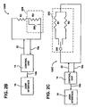
Figure 2B is a simplified schematic diagram showing circuitry of a sensor probe of the sensor system ofFigure 1 according to a second embodiment; and -
Figure 2C is a simplified schematic diagram showing circuitry of a sensor probe of the sensor system ofFigure 1 according to a third embodiment. - The following description of the preferred embodiments is merely exemplary in nature and is in no way intended to limit the invention, its application, or uses.
-
Figure 1 generally depicts the major components of an exemplary chemiresistor sensor system at 10. Thesensor system 10 is generally comprised of achemiresistor sensor probe 12, acontrol unit 14, and auser interface 16. Thesensor probe 12 includestemperature compensating elements 20. - The
sensor probe 12 interacts with anexternal environment 17 to detect the presence of chemical compositions of interest, or target analytes 18. Thesensor probe 12 generates araw output signal 19a based on continuous detection ofanalytes 18 in theexternal environment 17. Theraw output signal 19a is processed by thecontrol unit 14. Thecontrol unit 14 transmits a calculatedoutput signal 19b to theuser interface 16 to relay analysis of theraw output signal 19a from thesensor probe 12. Thecontrol unit 14 supplies operating commands and a load, both represented at 22, to theprobe 12. - The
user interface 16 provides information to a user regarding the status of thesensor system 10, such as whether or not thesystem 10 detects the presence of thetarget analytes 18. Theuser interface 16 can be of a variety of different forms known in the art and can range from a simple alarm signal to a sophisticated computerized display. - The
sensor probe 12 can take the form of a variety of different sensor probes. For example, thesensor probe 12 can take the form of any of the sensor probes described inU.S. Patent Application No. 10/412,602 , (US 2004200722 ) titled Robust Chemiresistor Sensor and filed April 11, 2003. U.S.. - The
sensor probe 12 includes a conductive sensor element or film. The sensor film can be any suitable sensor film known in the art, such as those described inU.S. Patent App. No. 10/411,805 ,US 200420856which was filed on April 11, 2003 and is titled "Vapor Sensor and Materials Therefor." The sensor film absorbs thetarget analytes 18 and changes resistance upon absorbing the target analytes. - With additional reference to
Figure 2 , a simplified schematic diagram showing the circuitry of thesensor probe 12 is illustrated at 100. -
Figure 2A illustrates the circuitry of thesensor probe 12 according to a first embodiment at 100A. In the embodiment at 100A, thesensor probe 12 includes a first resistor R1, a second resistor R2, and a load regulating device or switch SW. The second resistor R2 and the switch SW are part of thetemperature compensation element 20A. - The first resistor R1 is provided by the sensor film. The second resistor R2 can be a second sensor film or any conventional resistor known in the art. The first resistor R1 and the second resistor R2 are arranged electrically in parallel. The resistance of the
circuit 100A is monitored by thecontrol unit 14. - The switch SW is movable between an open position and a closed position. The switch SW opens and closes in response to changes in ambient temperature. The switch SW can be any suitable switch known in the art, such as a stand-alone thermostatically activated switch or a switch controlled by external means. In some embodiments, the switch SW is a bimetal temperature control, such as any one of the 36T series of bimetal temperature controls from Therm-O-Disc Inc. of Mansfield, Ohio, for example.
- When the switch SW is in the closed position the second resistor R2 is connected electrically in parallel with the first resistor R1. When the switch SW is in the open position the resistor R2 is removed from the circuit, leaving only the first resistor R1 in the circuit.
- An additional embodiment of the circuitry of the
sensor probe 12 is illustrated inFigure 2B at reference numeral 100B. The circuit 100B includes the same elements as thecircuit 100A. As with thecircuit 100A, thetemperature compensation elements 20B include the second resistor R2 and the switch SW. The only substantial difference between thecircuit 100A and the circuit 100B is the manner in which the different elements are arranged. Therefore, the general description of the resistors R1 and R2 and the switch SW set forth in connection with the description of thecircuit 100A equally applies to the circuit 100B. - In the circuit 100B, the first resistor R1 and the second resistor R2 are arranged electrically in series. The switch SW is positioned to provide a low resistance bypass around the resistor R2. When the switch SW is open the load passes through both the first resistor R1 and the second resistor R2 in series to increase the overall resistance of the circuit 100B. When the switch SW is closed the load bypasses the second resistor R2 to remove the second resistor R2 from the circuit 100B and lower the overall resistance of the circuit 100B.
-
Figure 2C illustrates an additional embodiment of the circuitry of thesensor probe 12 atreference numeral 100C. Thecircuit 100C includes all of the same elements as thecircuit 100A. However, in thecircuit 100C the second resistor R2, like the first resistor R1, is provided by the sensor film of theprobe 12 with the first resistor R1 and the second resistor R2 having different resistances. Thetemperature compensation elements 20 include the switch SW and both resistors R1 and R2. The general description of the resistor R1 and the switch SW set forth in connection with the description of thecircuit 100A equally applies to thecircuit 100C. - In the
circuit 100C, the first and second resistors R1 and R2 are on independent load paths. Actuation of the switch SW places either the first resistor R1 or the second resistor R2 in thecircuit 100C. Specifically, the switch can be moved between a first position in which it contacts the load path of the first resistor R1 to include the first resistor R1 in thecircuit 100C and a second position in which it contacts the load path of the second resistor R2 to include the second resistor R2 in thecircuit 100C. The first resistor has a first resistance and the second resistor has a second resistance that is lower than the first resistance. - The circuit 100 may take the form of numerous other embodiments in addition to those provided at
reference numerals - Operation of the
sensor system 10 will now be described. The target analytes 18 are absorbed by the sensor film of theprobe 12 when theanalytes 18 are present in theexternal environment 17. The sensor film swells upon absorption of theanalytes 18. As the film swells, the distance between conductive particles embedded in the sensor film increases, thus changing the resistance R1 (or R2 in thecircuit 100C) of the film as measured by thecontrol unit 14. - Upon detecting a change in resistance, the
control unit 14 transmits acalculated output 19b to theuser interface 16 instructing theuser interface 16 to alert the user that thetarget analytes 18 have been detected by theprobe 12. Theuser interface 16 may be any appropriate interface capable of providing an alert to the user. Theinterface 16 may range in complexity from a simple alarm to a complex computer providing audio and visual alerts. - Operation of the
sensor probe 12 outfitted with some of the different sensor circuits 100 set forth herein will now be described. - With respect to the
circuit 100A, the switch SW opens and closes in response to changes in ambient temperature. If the first and second resistors R1 and R2 both have a positive temperature coefficient of resistance, such that the resistance increases as temperature increases, the switch SW remains in an open position when the ambient temperature is at or below a predetermined temperature value or threshold. When the switch SW is in the open position only the resistor R1 is in the circuit. Operation of the switch SW can be controlled by thecontrol unit 14 and/or the switch SW can be a stand-alone thermostatically activated switch. - When the ambient temperature rises above the predetermined temperature threshold, the switch SW closes to place the second resistor R2 in parallel with the first resistor R1. Having the first and second resistors R1 and R2 in parallel lowers the overall resistance of the
circuit 100A below the individual resistance of the first and second resistors R1 and R2 to take into account the increased resistance of the resistors R1 and R2 caused by the increase in ambient temperature. - When the ambient temperature drops back to or below the predetermined temperature, the switch opens to return the resistance of the
circuit 100A to its optimal resistance for the predetermined temperature. - If the first and second resistors R1 and R2 both have a negative temperature coefficient of resistance, such that the resistance decreases as the temperature increases, the operation of the switch SW is reversed. Specifically, the switch SW opens when the ambient temperature rises above the predetermined temperature and closes when the ambient temperature is at or below the predetermined temperature.
- With respect to the circuit 100B, the switch SW remains open at or below a predetermined ambient temperature threshold or value so that the first resistor R1 and the second resistor R2 are electrically in series to maintain the overall resistance of the circuit 100B at an acceptable resistance. If the first and second resistors R1 and R2 both have a positive temperature coefficient of resistance, such that the resistance increases as temperature increases, the switch SW closes when the ambient temperature increases above a predetermined temperature threshold. Closing the switch effectively removes the second resistor R2 from the circuit and lowers the overall resistance of the circuit 100B to counteract the increase in resistance caused by the increase in ambient temperature.
- If the first and second resistors R1 and R2 both have a negative temperature coefficient of resistance, such that the resistance decreases as the temperature increases, the operation of the switch SW is reversed. Specifically, the switch SW remains closed at standard or lower ambient temperatures and opens when the ambient temperature rises above a predetermined temperature threshold.
- With respect to the
circuit 100C, if the first and second resistors R1 and R2 each have a positive coefficient of resistance, the switch SW is placed in the first position at or below a predetermined ambient temperature value or threshold to include the first resistor R1 in thecircuit 100C. When the ambient temperature rises above the predetermined temperature threshold the switch moves to the second position to remove the first resistor R1 from the circuit and include the second resistor R2 in the circuit. Replacing the first resistor R1 with the second resistor R2 lowers the overall resistance of thecircuit 100C because the second resistor R2 has a lower resistance than the first resistor R1. - If the first and second resistors R1 and R2 have a negative temperature coefficient of resistance, the operation of the switch SW in response to changes in ambient temperature is reversed. Specifically, the switch SW moves to the second position when the ambient temperature is at or below the predetermined temperature threshold. The switch moves to the first position when the temperature rises above the predetermined temperature threshold.
- The circuits 100 compensate for changes in the resistance of the first and second resistors R1 and R2 that occurs due to changes in ambient temperature. Therefore, the
sensor system 10 is able to distinguish between changes in resistance caused by the presence of thetarget analytes 18 versus changes in resistance caused by changes in ambient temperature. As a result, thesensor system 10 can detect the presence of theanalytes 18 with improved accuracy. - The description of the invention is merely exemplary in nature and, thus, variations that do not depart from the gist of the invention are intended to be within the scope of the invention. Such variations are not to be regarded as a departure from the scope of the invention.
Claims (15)
- A chemiresistor sensor system for detecting the presence of one or more analytes comprising:- a first resistor;- a second resistor; and- a thermally responsive load regulating device that comprises a switch that manages an electrical load current across at least one of said first resistor and said second resistor to change the resistance of a sensing circuit that includes said first resistor and said second resistor;wherein at least one of said first resistor and said second resistor is a sensing element with a resistance that changes in response to the presence of one or more of the analytes;
wherein said load regulating device prevents passage of the electrical load current across said first resistor when the ambient temperature is at a first value; and
wherein said load regulating device permits passage of the electrical load current across said first resistor when the ambient temperature is at a second value. - The chemiresistor sensor system of claim 1, wherein said first resistor is electrically in parallel with said second resistor.
- The chemiresistor sensor system of claim 1, wherein said first resistor is electrically in series with said second resistor.
- The chemiresistor sensor system of any of claims 1-3, wherein said sensing element comprises a crosslinked, polymeric matrix sensor film.
- The chemiresistor sensor system of any of claims 1-4, wherein said first value Is greater than said second value.
- The chemiresistor sensor system of any of claims 1-4, wherein said first value is less than said second value.
- A chemiresistor sensor system circuit for detecting the presence of an analyte, said circuit comprising:- a first sensing element having a first resistance that changes in response to the presence of the analyte;- a second sensing element having a second resistance that changes in response to the presence of the analyte, said second resistance is different from said first resistance; and- a thermally responsive load regulating device that includes a switch;wherein at a first ambient temperature the operation of the switch
prevents the electrical load current from passing from passing across the second sensing element; and
wherein at a second ambient temperature the operation of the switch enables the electrical load current to pass across both the first sensing element and the second sensing element. - The chemiresistor sensor system circuit of claim 7, wherein at least one of said first sensing element and said second sensing element includes a crosslinked, polymeric matrix sensor film.
- The chemiresistor sensor system circuit of claim 7 or 8, wherein said switch is a stand-alone thermally activated switch.
- The chemiresistor sensor circuit of any of claims 7-9, wherein said switch is a bimetal switch.
- A method for compensating for the effects of ambient temperature on a chemiresistor sensor circuit system having a first sensing element with a resistance that changes in response to the presence of one or more analytes, the method comprising:- determining the ambient temperature of the area surrounding the sensor circuit system;- actuating a thermally responsive load regulating device that includes a switch to add a resistor into the sensor circuit system if the ambient temperature is at a first value; and- actuating the switch to remove the resistor from the sensing circuit system if the ambient temperature is at a second value that is different from the first value,wherein the resistor compensates for a change in the resistance of the first sensing element when the ambient temperature changes from the first value to the second value.
- The method of claim 11, further comprising adding the resistor to the sensor circuit system so that the resistor is electrically in parallel with the first sensing element.
- The method of claim 11 or 12, further comprising adding the resistor to the sensor circuit system so that the resistor is electrically in series with the first sensing element.
- The method of any of claims 11-13, wherein said resistor is a second sensing element.
- The method of any of claims 11-14, further comprising including a crosslinked, polymeric matrix sensor film in each of the first sensing element and the second sensing element.
Applications Claiming Priority (1)
| Application Number | Priority Date | Filing Date | Title |
|---|---|---|---|
| US11/286,985 US7265560B2 (en) | 2005-11-23 | 2005-11-23 | Temperature compensated vapor sensor |
Publications (3)
| Publication Number | Publication Date |
|---|---|
| EP1790978A1 EP1790978A1 (en) | 2007-05-30 |
| EP1790978B1 true EP1790978B1 (en) | 2013-01-02 |
| EP1790978B8 EP1790978B8 (en) | 2013-04-10 |
Family
ID=37759961
Family Applications (1)
| Application Number | Title | Priority Date | Filing Date |
|---|---|---|---|
| EP06024012.4A Not-in-force EP1790978B8 (en) | 2005-11-23 | 2006-11-20 | Temperature compensated vapor sensor |
Country Status (5)
| Country | Link |
|---|---|
| US (1) | US7265560B2 (en) |
| EP (1) | EP1790978B8 (en) |
| JP (1) | JP5107558B2 (en) |
| CN (1) | CN201043961Y (en) |
| CA (1) | CA2562732C (en) |
Families Citing this family (6)
| Publication number | Priority date | Publication date | Assignee | Title |
|---|---|---|---|---|
| TWI323032B (en) * | 2006-07-25 | 2010-04-01 | Siliconmotion Inc | A circuit for compensating resistance variation and a method for tuning frequency thereof |
| WO2015054784A1 (en) | 2013-10-15 | 2015-04-23 | 1835963 Alberta Ltd. | Sensing element compositions and sensor system for detecting and monitoring structures for hydrocarbons |
| CA3000385A1 (en) | 2017-04-11 | 2018-10-11 | Syscor Controls & Automation Inc. | Polymer absorption sensor having low cross-sensitivity |
| US11331019B2 (en) | 2017-08-07 | 2022-05-17 | The Research Foundation For The State University Of New York | Nanoparticle sensor having a nanofibrous membrane scaffold |
| US11092497B2 (en) | 2018-10-31 | 2021-08-17 | Taiwan Semiconductor Manufacturing Company Limited | Temperature protection circuit |
| JP7731857B2 (en) * | 2022-08-25 | 2025-09-01 | 株式会社東芝 | Sensors and Sensor Systems |
Family Cites Families (18)
| Publication number | Priority date | Publication date | Assignee | Title |
|---|---|---|---|---|
| GB1259566A (en) | 1970-07-13 | 1972-01-05 | ||
| GB1479925A (en) | 1974-08-24 | 1977-07-13 | Westfaelische Berggewerkschaft | Method and apparatus for determining the concentration of one or more than one gaseous component in a mixture of gases |
| JPS592080B2 (en) * | 1975-09-27 | 1984-01-17 | 株式会社山武 | Nisenshikisitsudohatsushinki |
| JPS54134698A (en) | 1978-04-11 | 1979-10-19 | Mitsubishi Electric Corp | Semiconductor gas detector |
| JP2556367B2 (en) * | 1988-12-02 | 1996-11-20 | 株式会社ジャパンエナジー | Electronic thermo-hygrometer |
| JPH06160318A (en) * | 1992-04-23 | 1994-06-07 | Nippon Ceramic Co Ltd | Gas sensor temperature compensation circuit |
| JP2889910B2 (en) * | 1993-10-18 | 1999-05-10 | リコーエレメックス株式会社 | Atmosphere detector |
| US5464739A (en) * | 1994-08-22 | 1995-11-07 | Bayer Corporation | Composition method for determining the presence of leukocyte cells, esterase or protease in a test sample |
| EP0698786A1 (en) | 1994-08-23 | 1996-02-28 | RICOH SEIKI COMPANY, Ltd. | Atmosphere measuring device and flow sensor |
| JP3343801B2 (en) * | 1994-12-29 | 2002-11-11 | 光照 木村 | Humidity sensor |
| US5864458A (en) * | 1995-09-14 | 1999-01-26 | Raychem Corporation | Overcurrent protection circuits comprising combinations of PTC devices and switches |
| JP3933321B2 (en) * | 1997-09-03 | 2007-06-20 | フィガロ技研株式会社 | Gas detection method and apparatus |
| JP3942059B2 (en) * | 1997-09-03 | 2007-07-11 | フィガロ技研株式会社 | Gas detector |
| JP2002190607A (en) * | 2000-12-22 | 2002-07-05 | Denso Corp | Semiconductor device and manufacturing method thereof |
| JP2003185613A (en) * | 2001-12-18 | 2003-07-03 | Fis Inc | Portable gas detector |
| DE10254852A1 (en) | 2002-11-25 | 2004-06-03 | Robert Bosch Gmbh | Circuit arrangement for sensor evaluation and method for evaluating a plurality of sensors |
| US7138090B2 (en) | 2003-04-11 | 2006-11-21 | Therm-O-Disc, Incorporated | Vapor sensor and materials therefor |
| US7126355B2 (en) * | 2004-05-31 | 2006-10-24 | Yamaha Hatsudoki Kabushiki Kaisha | Physical quantity sensing device with bridge circuit and temperature compensating method |
-
2005
- 2005-11-23 US US11/286,985 patent/US7265560B2/en not_active Expired - Lifetime
-
2006
- 2006-10-05 CA CA2562732A patent/CA2562732C/en active Active
- 2006-11-10 CN CNU2006201474237U patent/CN201043961Y/en not_active Expired - Lifetime
- 2006-11-16 JP JP2006309826A patent/JP5107558B2/en not_active Expired - Fee Related
- 2006-11-20 EP EP06024012.4A patent/EP1790978B8/en not_active Not-in-force
Also Published As
| Publication number | Publication date |
|---|---|
| US20070117207A1 (en) | 2007-05-24 |
| JP2007147611A (en) | 2007-06-14 |
| US7265560B2 (en) | 2007-09-04 |
| CA2562732C (en) | 2013-02-19 |
| CA2562732A1 (en) | 2007-05-23 |
| EP1790978A1 (en) | 2007-05-30 |
| EP1790978B8 (en) | 2013-04-10 |
| JP5107558B2 (en) | 2012-12-26 |
| CN201043961Y (en) | 2008-04-02 |
Similar Documents
| Publication | Publication Date | Title |
|---|---|---|
| EP2239562B1 (en) | Checking electrochemical gas sensors | |
| US7607823B2 (en) | Leak detector comprising a self-heated thermistor control circuit | |
| US20250067714A1 (en) | Determination of sensor operational status via sensor interrogation | |
| EP2195646B1 (en) | Gas measuring device and method of manufacturing the same | |
| EP2012115A2 (en) | Chemiresistor sensor system compensated for temperature and aging effects | |
| JP5622352B2 (en) | Electrochemical sensor with zero calibration function and calibration method | |
| CN114594132B (en) | Thermal sensor device and method for detecting faults in thermal sensor device | |
| US7265560B2 (en) | Temperature compensated vapor sensor | |
| US8505354B2 (en) | Compensated gas detectors | |
| WO2009045447A2 (en) | Gas measuring device and method of operating the same | |
| AU2006332047B2 (en) | Linear fire-detector alarming system based on data fusion and the method | |
| CN201311407Y (en) | Chemical resistor sensor system capable of compensating temperature and aging effect | |
| JP3882297B2 (en) | Gas measuring device | |
| US20120019308A1 (en) | Pressure switch with temperature enable function | |
| KR100638951B1 (en) | Sensor device and method for measuring electrical resistance of an electrical supply lead to sensor elements | |
| US20090213517A1 (en) | Switching device for switching at least one current | |
| JP2007147611A5 (en) | ||
| JP5062657B2 (en) | Abnormality detection device and abnormality detection method for sensor chip with heater | |
| Ansuini | Dual Mode Corrosion Monitors | |
| JP2001264280A (en) | Method of diagnosing sensitivity deterioration of gas detector, and gas detector having sensitivity deterioration diagnosis function | |
| JP2002055071A (en) | Gas detection performance diagnosis method and gas detection device | |
| KR20060069895A (en) | Engine oil deterioration detection and alarm | |
| JPH0580027A (en) | Electrochemical gas sensor | |
| JP2007093365A (en) | Voltage detection element and voltage detection method | |
| GB2484089A (en) | Dual action parallel sensor |
Legal Events
| Date | Code | Title | Description |
|---|---|---|---|
| PUAI | Public reference made under article 153(3) epc to a published international application that has entered the european phase |
Free format text: ORIGINAL CODE: 0009012 |
|
| AK | Designated contracting states |
Kind code of ref document: A1 Designated state(s): AT BE BG CH CY CZ DE DK EE ES FI FR GB GR HU IE IS IT LI LT LU LV MC NL PL PT RO SE SI SK TR |
|
| AX | Request for extension of the european patent |
Extension state: AL BA HR MK YU |
|
| 17P | Request for examination filed |
Effective date: 20071113 |
|
| 17Q | First examination report despatched |
Effective date: 20071221 |
|
| AKX | Designation fees paid |
Designated state(s): AT BE BG CH CY CZ DE DK EE ES FI FR GB GR HU IE IS IT LI LT LU LV MC NL PL PT RO SE SI SK TR |
|
| GRAP | Despatch of communication of intention to grant a patent |
Free format text: ORIGINAL CODE: EPIDOSNIGR1 |
|
| GRAS | Grant fee paid |
Free format text: ORIGINAL CODE: EPIDOSNIGR3 |
|
| GRAP | Despatch of communication of intention to grant a patent |
Free format text: ORIGINAL CODE: EPIDOSNIGR1 |
|
| GRAA | (expected) grant |
Free format text: ORIGINAL CODE: 0009210 |
|
| AK | Designated contracting states |
Kind code of ref document: B1 Designated state(s): AT BE BG CH CY CZ DE DK EE ES FI FR GB GR HU IE IS IT LI LT LU LV MC NL PL PT RO SE SI SK TR |
|
| REG | Reference to a national code |
Ref country code: GB Ref legal event code: FG4D |
|
| REG | Reference to a national code |
Ref country code: CH Ref legal event code: EP Ref country code: AT Ref legal event code: REF Ref document number: 591869 Country of ref document: AT Kind code of ref document: T Effective date: 20130115 |
|
| REG | Reference to a national code |
Ref country code: IE Ref legal event code: FG4D |
|
| REG | Reference to a national code |
Ref country code: DE Ref legal event code: R096 Ref document number: 602006033917 Country of ref document: DE Effective date: 20130228 |
|
| REG | Reference to a national code |
Ref country code: AT Ref legal event code: MK05 Ref document number: 591869 Country of ref document: AT Kind code of ref document: T Effective date: 20130102 |
|
| REG | Reference to a national code |
Ref country code: NL Ref legal event code: VDEP Effective date: 20130102 |
|
| PG25 | Lapsed in a contracting state [announced via postgrant information from national office to epo] |
Ref country code: SI Free format text: LAPSE BECAUSE OF FAILURE TO SUBMIT A TRANSLATION OF THE DESCRIPTION OR TO PAY THE FEE WITHIN THE PRESCRIBED TIME-LIMIT Effective date: 20130102 |
|
| REG | Reference to a national code |
Ref country code: LT Ref legal event code: MG4D |
|
| PG25 | Lapsed in a contracting state [announced via postgrant information from national office to epo] |
Ref country code: LT Free format text: LAPSE BECAUSE OF FAILURE TO SUBMIT A TRANSLATION OF THE DESCRIPTION OR TO PAY THE FEE WITHIN THE PRESCRIBED TIME-LIMIT Effective date: 20130102 Ref country code: SE Free format text: LAPSE BECAUSE OF FAILURE TO SUBMIT A TRANSLATION OF THE DESCRIPTION OR TO PAY THE FEE WITHIN THE PRESCRIBED TIME-LIMIT Effective date: 20130102 Ref country code: CZ Free format text: LAPSE BECAUSE OF FAILURE TO SUBMIT A TRANSLATION OF THE DESCRIPTION OR TO PAY THE FEE WITHIN THE PRESCRIBED TIME-LIMIT Effective date: 20130102 Ref country code: BE Free format text: LAPSE BECAUSE OF FAILURE TO SUBMIT A TRANSLATION OF THE DESCRIPTION OR TO PAY THE FEE WITHIN THE PRESCRIBED TIME-LIMIT Effective date: 20130102 Ref country code: BG Free format text: LAPSE BECAUSE OF FAILURE TO SUBMIT A TRANSLATION OF THE DESCRIPTION OR TO PAY THE FEE WITHIN THE PRESCRIBED TIME-LIMIT Effective date: 20130402 Ref country code: IS Free format text: LAPSE BECAUSE OF FAILURE TO SUBMIT A TRANSLATION OF THE DESCRIPTION OR TO PAY THE FEE WITHIN THE PRESCRIBED TIME-LIMIT Effective date: 20130502 Ref country code: ES Free format text: LAPSE BECAUSE OF FAILURE TO SUBMIT A TRANSLATION OF THE DESCRIPTION OR TO PAY THE FEE WITHIN THE PRESCRIBED TIME-LIMIT Effective date: 20130413 Ref country code: AT Free format text: LAPSE BECAUSE OF FAILURE TO SUBMIT A TRANSLATION OF THE DESCRIPTION OR TO PAY THE FEE WITHIN THE PRESCRIBED TIME-LIMIT Effective date: 20130102 |
|
| PG25 | Lapsed in a contracting state [announced via postgrant information from national office to epo] |
Ref country code: PT Free format text: LAPSE BECAUSE OF FAILURE TO SUBMIT A TRANSLATION OF THE DESCRIPTION OR TO PAY THE FEE WITHIN THE PRESCRIBED TIME-LIMIT Effective date: 20130502 Ref country code: GR Free format text: LAPSE BECAUSE OF FAILURE TO SUBMIT A TRANSLATION OF THE DESCRIPTION OR TO PAY THE FEE WITHIN THE PRESCRIBED TIME-LIMIT Effective date: 20130403 Ref country code: PL Free format text: LAPSE BECAUSE OF FAILURE TO SUBMIT A TRANSLATION OF THE DESCRIPTION OR TO PAY THE FEE WITHIN THE PRESCRIBED TIME-LIMIT Effective date: 20130102 Ref country code: LV Free format text: LAPSE BECAUSE OF FAILURE TO SUBMIT A TRANSLATION OF THE DESCRIPTION OR TO PAY THE FEE WITHIN THE PRESCRIBED TIME-LIMIT Effective date: 20130102 Ref country code: FI Free format text: LAPSE BECAUSE OF FAILURE TO SUBMIT A TRANSLATION OF THE DESCRIPTION OR TO PAY THE FEE WITHIN THE PRESCRIBED TIME-LIMIT Effective date: 20130102 Ref country code: NL Free format text: LAPSE BECAUSE OF FAILURE TO SUBMIT A TRANSLATION OF THE DESCRIPTION OR TO PAY THE FEE WITHIN THE PRESCRIBED TIME-LIMIT Effective date: 20130102 |
|
| PG25 | Lapsed in a contracting state [announced via postgrant information from national office to epo] |
Ref country code: DK Free format text: LAPSE BECAUSE OF FAILURE TO SUBMIT A TRANSLATION OF THE DESCRIPTION OR TO PAY THE FEE WITHIN THE PRESCRIBED TIME-LIMIT Effective date: 20130102 Ref country code: EE Free format text: LAPSE BECAUSE OF FAILURE TO SUBMIT A TRANSLATION OF THE DESCRIPTION OR TO PAY THE FEE WITHIN THE PRESCRIBED TIME-LIMIT Effective date: 20130102 Ref country code: RO Free format text: LAPSE BECAUSE OF FAILURE TO SUBMIT A TRANSLATION OF THE DESCRIPTION OR TO PAY THE FEE WITHIN THE PRESCRIBED TIME-LIMIT Effective date: 20130102 Ref country code: SK Free format text: LAPSE BECAUSE OF FAILURE TO SUBMIT A TRANSLATION OF THE DESCRIPTION OR TO PAY THE FEE WITHIN THE PRESCRIBED TIME-LIMIT Effective date: 20130102 |
|
| PLBE | No opposition filed within time limit |
Free format text: ORIGINAL CODE: 0009261 |
|
| STAA | Information on the status of an ep patent application or granted ep patent |
Free format text: STATUS: NO OPPOSITION FILED WITHIN TIME LIMIT |
|
| 26N | No opposition filed |
Effective date: 20131003 |
|
| REG | Reference to a national code |
Ref country code: DE Ref legal event code: R097 Ref document number: 602006033917 Country of ref document: DE Effective date: 20131003 |
|
| REG | Reference to a national code |
Ref country code: CH Ref legal event code: PL |
|
| PG25 | Lapsed in a contracting state [announced via postgrant information from national office to epo] |
Ref country code: CH Free format text: LAPSE BECAUSE OF NON-PAYMENT OF DUE FEES Effective date: 20131130 Ref country code: LI Free format text: LAPSE BECAUSE OF NON-PAYMENT OF DUE FEES Effective date: 20131130 Ref country code: MC Free format text: LAPSE BECAUSE OF FAILURE TO SUBMIT A TRANSLATION OF THE DESCRIPTION OR TO PAY THE FEE WITHIN THE PRESCRIBED TIME-LIMIT Effective date: 20130102 |
|
| REG | Reference to a national code |
Ref country code: IE Ref legal event code: MM4A |
|
| PG25 | Lapsed in a contracting state [announced via postgrant information from national office to epo] |
Ref country code: IE Free format text: LAPSE BECAUSE OF NON-PAYMENT OF DUE FEES Effective date: 20131120 |
|
| PG25 | Lapsed in a contracting state [announced via postgrant information from national office to epo] |
Ref country code: TR Free format text: LAPSE BECAUSE OF FAILURE TO SUBMIT A TRANSLATION OF THE DESCRIPTION OR TO PAY THE FEE WITHIN THE PRESCRIBED TIME-LIMIT Effective date: 20130102 Ref country code: CY Free format text: LAPSE BECAUSE OF FAILURE TO SUBMIT A TRANSLATION OF THE DESCRIPTION OR TO PAY THE FEE WITHIN THE PRESCRIBED TIME-LIMIT Effective date: 20130102 |
|
| PG25 | Lapsed in a contracting state [announced via postgrant information from national office to epo] |
Ref country code: HU Free format text: LAPSE BECAUSE OF FAILURE TO SUBMIT A TRANSLATION OF THE DESCRIPTION OR TO PAY THE FEE WITHIN THE PRESCRIBED TIME-LIMIT; INVALID AB INITIO Effective date: 20061120 Ref country code: LU Free format text: LAPSE BECAUSE OF NON-PAYMENT OF DUE FEES Effective date: 20131120 |
|
| REG | Reference to a national code |
Ref country code: FR Ref legal event code: PLFP Year of fee payment: 10 |
|
| REG | Reference to a national code |
Ref country code: FR Ref legal event code: PLFP Year of fee payment: 11 |
|
| REG | Reference to a national code |
Ref country code: FR Ref legal event code: PLFP Year of fee payment: 12 |
|
| P01 | Opt-out of the competence of the unified patent court (upc) registered |
Effective date: 20230515 |
|
| PGFP | Annual fee paid to national office [announced via postgrant information from national office to epo] |
Ref country code: GB Payment date: 20231127 Year of fee payment: 18 |
|
| PGFP | Annual fee paid to national office [announced via postgrant information from national office to epo] |
Ref country code: IT Payment date: 20231122 Year of fee payment: 18 Ref country code: FR Payment date: 20231127 Year of fee payment: 18 Ref country code: DE Payment date: 20231129 Year of fee payment: 18 |
|
| REG | Reference to a national code |
Ref country code: DE Ref legal event code: R119 Ref document number: 602006033917 Country of ref document: DE |
|
| GBPC | Gb: european patent ceased through non-payment of renewal fee |
Effective date: 20241120 |
|
| PG25 | Lapsed in a contracting state [announced via postgrant information from national office to epo] |
Ref country code: DE Free format text: LAPSE BECAUSE OF NON-PAYMENT OF DUE FEES Effective date: 20250603 |
|
| PG25 | Lapsed in a contracting state [announced via postgrant information from national office to epo] |
Ref country code: IT Free format text: LAPSE BECAUSE OF NON-PAYMENT OF DUE FEES Effective date: 20241120 |
|
| PG25 | Lapsed in a contracting state [announced via postgrant information from national office to epo] |
Ref country code: GB Free format text: LAPSE BECAUSE OF NON-PAYMENT OF DUE FEES Effective date: 20241120 |
|
| PG25 | Lapsed in a contracting state [announced via postgrant information from national office to epo] |
Ref country code: FR Free format text: LAPSE BECAUSE OF NON-PAYMENT OF DUE FEES Effective date: 20241130 |