EP1788700A1 - Method for double sampling loop negative feedback and double sampling negative feedback amplifier - Google Patents
Method for double sampling loop negative feedback and double sampling negative feedback amplifier Download PDFInfo
- Publication number
- EP1788700A1 EP1788700A1 EP05774340A EP05774340A EP1788700A1 EP 1788700 A1 EP1788700 A1 EP 1788700A1 EP 05774340 A EP05774340 A EP 05774340A EP 05774340 A EP05774340 A EP 05774340A EP 1788700 A1 EP1788700 A1 EP 1788700A1
- Authority
- EP
- European Patent Office
- Prior art keywords
- signal
- frequency
- feedback
- double
- sampling
- Prior art date
- Legal status (The legal status is an assumption and is not a legal conclusion. Google has not performed a legal analysis and makes no representation as to the accuracy of the status listed.)
- Granted
Links
Images


Classifications
-
- H—ELECTRICITY
- H03—ELECTRONIC CIRCUITRY
- H03F—AMPLIFIERS
- H03F3/00—Amplifiers with only discharge tubes or only semiconductor devices as amplifying elements
- H03F3/45—Differential amplifiers
- H03F3/45071—Differential amplifiers with semiconductor devices only
- H03F3/45076—Differential amplifiers with semiconductor devices only characterised by the way of implementation of the active amplifying circuit in the differential amplifier
- H03F3/4508—Differential amplifiers with semiconductor devices only characterised by the way of implementation of the active amplifying circuit in the differential amplifier using bipolar transistors as the active amplifying circuit
- H03F3/45085—Long tailed pairs
-
- H—ELECTRICITY
- H03—ELECTRONIC CIRCUITRY
- H03F—AMPLIFIERS
- H03F1/00—Details of amplifiers with only discharge tubes, only semiconductor devices or only unspecified devices as amplifying elements
- H03F1/32—Modifications of amplifiers to reduce non-linear distortion
-
- H—ELECTRICITY
- H03—ELECTRONIC CIRCUITRY
- H03F—AMPLIFIERS
- H03F1/00—Details of amplifiers with only discharge tubes, only semiconductor devices or only unspecified devices as amplifying elements
- H03F1/32—Modifications of amplifiers to reduce non-linear distortion
- H03F1/3211—Modifications of amplifiers to reduce non-linear distortion in differential amplifiers
-
- H—ELECTRICITY
- H03—ELECTRONIC CIRCUITRY
- H03F—AMPLIFIERS
- H03F1/00—Details of amplifiers with only discharge tubes, only semiconductor devices or only unspecified devices as amplifying elements
- H03F1/34—Negative-feedback-circuit arrangements with or without positive feedback
-
- H—ELECTRICITY
- H03—ELECTRONIC CIRCUITRY
- H03F—AMPLIFIERS
- H03F3/00—Amplifiers with only discharge tubes or only semiconductor devices as amplifying elements
- H03F3/20—Power amplifiers, e.g. Class B amplifiers, Class C amplifiers
-
- H—ELECTRICITY
- H03—ELECTRONIC CIRCUITRY
- H03F—AMPLIFIERS
- H03F3/00—Amplifiers with only discharge tubes or only semiconductor devices as amplifying elements
- H03F3/30—Single-ended push-pull [SEPP] amplifiers; Phase-splitters therefor
- H03F3/3069—Single-ended push-pull [SEPP] amplifiers; Phase-splitters therefor the emitters of complementary power transistors being connected to the output
- H03F3/3071—Single-ended push-pull [SEPP] amplifiers; Phase-splitters therefor the emitters of complementary power transistors being connected to the output with asymmetrical driving of the end stage
- H03F3/3072—Single-ended push-pull [SEPP] amplifiers; Phase-splitters therefor the emitters of complementary power transistors being connected to the output with asymmetrical driving of the end stage using Darlington transistors
-
- H—ELECTRICITY
- H03—ELECTRONIC CIRCUITRY
- H03F—AMPLIFIERS
- H03F3/00—Amplifiers with only discharge tubes or only semiconductor devices as amplifying elements
- H03F3/30—Single-ended push-pull [SEPP] amplifiers; Phase-splitters therefor
- H03F3/3069—Single-ended push-pull [SEPP] amplifiers; Phase-splitters therefor the emitters of complementary power transistors being connected to the output
- H03F3/3071—Single-ended push-pull [SEPP] amplifiers; Phase-splitters therefor the emitters of complementary power transistors being connected to the output with asymmetrical driving of the end stage
- H03F3/3074—Single-ended push-pull [SEPP] amplifiers; Phase-splitters therefor the emitters of complementary power transistors being connected to the output with asymmetrical driving of the end stage using parallel power transistors
-
- H—ELECTRICITY
- H03—ELECTRONIC CIRCUITRY
- H03F—AMPLIFIERS
- H03F3/00—Amplifiers with only discharge tubes or only semiconductor devices as amplifying elements
- H03F3/45—Differential amplifiers
- H03F3/45071—Differential amplifiers with semiconductor devices only
- H03F3/45076—Differential amplifiers with semiconductor devices only characterised by the way of implementation of the active amplifying circuit in the differential amplifier
- H03F3/4508—Differential amplifiers with semiconductor devices only characterised by the way of implementation of the active amplifying circuit in the differential amplifier using bipolar transistors as the active amplifying circuit
- H03F3/45085—Long tailed pairs
- H03F3/45094—Folded cascode stages
Definitions
- the invention relates to an amplifier, and more particularly, to a method for double sampling loop negative feedback and double sampling negative feedback amplifier.
- Loop negative feedback is an important method for improving performance of a linear amplifier.
- larger loop feedback depth results in less distortion of the amplifier.
- further increase in feedback depth is limited by stability of the amplifier. That is to say, if the frequency of amplified signal is higher, the loop negative feedback depth obtainable will be smaller.
- the negative feedback depth of the audio power amplifier generally is only 10 times (20 db) at a frequency of 20 KHz. So that the capability of the loop negative feedback to lower amplifier distortion is limited.
- a main object of the invention is to provide a method for double sampling loop negative feedback, which is of advantageous to increase the feedback depth.
- Another object of the invention is to provide a double sampling negative feedback amplifier, which has good stability and small distortion characteristics.
- the invention provides a method for double sampling loop negative feedback, which comprises the steps: obtaining a low-frequency feedback signal from the output of the amplifier; obtaining a high-frequency feedback signal from part of the amplifier of which high frequency signal phase shift is low, wherein two-ways sampling signals have the same amplifying phase; combining the two sampling signals together using a series capacitor-inductor double signal combining circuit to form one signal, which having low phase shift at both high and low-frequency and being used for negative loop feedback.
- a damping resistor may be added to the series capacitor-inductor double signal combining circuit in parallel to the inductor or in series to the capacitor, or a damping resistor may be in parallel to the inductor and another resistor may be in series to the capacitor at a time.
- the invention provides a double sampling negative feedback amplifier, which comprises: a voltage amplifying circuit used to output voltage signal and transfer it to a high-speed buffer circuit and an output buffer circuit; an output buffer circuit used to achieve unit voltage gain, provide amplified output signal and low-frequency feedback signal; a high-speed buffer circuit used to achieve unit voltage gain and output high-frequency feedback signal to the input of the double signal combining circuit; a series capacitor-inductor double signal combining circuit used to combine the high and low-frequency feedback signals to form one-way compound feedback signal; and a feedback network for transfer the compound feedback signal to the inverting input of the voltage amplifying circuit.
- a damping resistor may be added to the series capacitor-inductor double signal combining circuit in parallel to the inductor or in series to the capacitor, or a damping resistor may be in parallel to the inductor and another damping resistor may be in series to the capacitor at a time.
- the double sampling negative feedback amplifier has a high-pass filter circuit incorporated in its high-frequency sampling channel in order to remove the low-frequency signal.
- the double sampling negative feedback amplifier further comprises a voltage gain stage prior to the output buffer circuit.
- the double sampling negative feedback amplifier further comprises a low-pass filter circuit prior to the low-frequency sampling node, which is utilized to remove the high-frequency signal from the low-frequency sampling channel.
- the stability at high-frequency will not be influenced by the output buffer circuit (stage) and changeable load, while the output buffer circuit and the load often have great impact on the feedback depth, thus the stability being affected only at low-frequency.
- the stability at high-frequency is affected by the high-frequency feedback sampling. Accordingly, the feedback depth of high-frequency is enhanced, i.e., more stable feedback depth can be obtained.
- the series capacitor-inductor double signal combining circuit signal ratio changes rapidly with frequency, it can achieve deeper feedback depth with a relatively narrow bandwidth of the output buffer circuit, thus reducing difficulty in realizing of deep negative feedback.
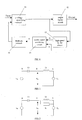
- Fig. 1 shows a schematic block illustrating a circuit of a double sampling negative feedback amplifier in accordance with a first embodiment of the invention
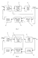
- Fig. 2 shows a schematic view illustrating a series capacitor-inductor double signal combining circuits in accordance with a first embodiment of the invention
- Fig. 3 shows a schematic view illustrating a series capacitor-inductor double signal combining circuits in accordance with a second embodiment of the invention
- Fig. 4 shows a schematic view illustrating a series capacitor-inductor double signal combining circuits in accordance with a third embodiment of the invention
- Fig. 5 shows a schematic view illustrating a series capacitor-inductor double signal combining circuits in accordance with a fourth embodiment of the invention
- Fig. 6 shows a schematic block illustrating a circuit of a double sampling negative feedback amplifier according to a second embodiment of the invention
- Fig. 7 shows a schematic block illustrating a circuit of a double sampling negative feedback amplifier according to a third embodiment of the invention.
- Fig. 8 shows a schematic block illustrating a circuit of a double sampling negative feedback amplifier according to a fourth embodiment of the invention.
- Fig. 9 shows a schematic block illustrating a circuit of a double sampling negative feedback amplifier according to a fifth embodiment of the invention.
- Fig. 10 shows an actual circuit for the double sampling negative feedback amplifier according to an embodiment of the invention.
- the invention provides a method for double sampling loop negative feedback, which includes the follow steps: (1) obtaining a low-frequency feedback signal from the output of the amplifier; obtaining a high-frequency feedback signal from part of the amplifier where high frequency signal phase shift is low, wherein two sampling signals have the same amplifying phase; combining the two sampling signals together using a series capacitor-inductor double signal combining circuit to form one signal, the signal having low phase shift at both high and low-frequency and being used for negative loop feedback.
- a damping resistor may be added to the series capacitor-inductor double signal combining circuit in parallel to the inductor or in series to the capacitor, or a damping resistor may be in parallel to the inductor and another resistor may be in series to the capacitor at a time.
- amplifying signal frequency band exists in low-frequency feedback frequency band.
- the output stage and the load will have impact on the stability of the negative feedback loop only at low-frequency band, while have no impact on the stability at high-frequency band, thus enabling to improve the feedback depth.
- the first method increasing crossover frequency of the double sampling circuit such that the bandwidth of the amplifier output (low-frequency sampling portion) will be widened.
- the method requires increase the bandwidth of the output stage.
- the second method utilizing a signal combining method which has characteristic of rapid frequency change.
- the method can take a lower crossover frequency, the requirement of bandwidth for the output stage is low and can obtain good stability.
- Fig. 1 shows a block illustrating a circuit of a double sampling negative feedback amplifier in accordance with a first,embodiment of the invention. Meaning and usage of each numeral is explained as follows:
- the voltage amplifying circuit used to output voltage signal and transfer it to a high-speed buffer circuit and an output buffer circuit.
- the voltage amplifying circuit is a differential input voltage amplifying stage.
- output buffer circuit used to achieve unit voltage gain, provide amplified output signal and low-frequency feedback sampling signal for a double signal combining circuit.
- high-speed buffer circuit used to achieve high speed unit voltage gain and output high-frequency feedback sampling signal to an input of the double signal combining circuit.
- double signal combining circuit used to combine the high and low-frequency feedback signals to form one-way compound feedback signal.
- the output signal of the voltage amplifying circuit 11 is delivered to the output buffer circuit 12 and the high-speed buffer circuit 13.
- the output buffer circuit 12 provides amplified output signal and low-frequency feedback sampling signal for the double signal combining circuit.
- the high-speed buffer circuit 13 provides high-frequency feedback sampling signal for the double signal combining circuit.
- the double signal combining circuit 14 composes the two-ways sampling signals into one-way signal, and then, the signal is delivered by feedback network 15 to the inverting input of the voltage amplifying circuit 11 to form a loop feedback.
- the main point of the design is a series capacitor-inductor double signal combining circuit.
- Fig. 2 shows a schematic view illustrating a series capacitor-inductor double signal combining circuit in accordance with an embodiment of the invention.
- the circuit is constructed by a capacitor C1 and an inductor L1 in series connection.
- One node B of the capacitor C1 is the high-frequency sampling input point
- one node A of the inductor L1 is the low-frequency sampling input point
- the connection node D of the capacitor C 1 and the inductor L1 is the compound signal output point.
- Nodes A, B and D shown in Fig. 2 are corresponding with the nodes A, B and D shown in Fig. 1, wherein
- V B High-frequency sampling input signal at node B of Fig. 1;
- V D Compound output feedback signal at node D of Fig. 1.
- ratio R AB the combining ratio of V A and V B , in compound signal V D
- the frequency is analyzed.
- Z C , Z L are impedance of Cl, L1 respectively
- V DA Z C Z C + Z L ⁇ V A
- V DB Z L Z C + Z L ⁇ V B
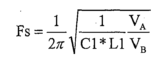
- R AB shows the relationship between ratio of low-frequency sampling component to high-frequency sampling component against the frequency for the compound feedback signal. Because the change of the ratio is proportional to the square of the frequency change, the method of the invention gains a feature of rapid frequency change, thus can achieving deeper feedback depth using narrower bandwidth in low-frequency feedback sampling. This is an important feature of the double signal combining circuit of the invention.
- the inductor L1 and the capacitor C1 are dynamic elements, the frequency characteristic of compound feedback signal at point D may have fluctuation in the band that between the high and low-sampling frequency, thus resulting in instability.
- the inductor L1 may connect with a damping resistor in parallel, or the capacitor C1 may connect in series with a damping resistor.
- the inner resistor of the buffer could be used as the resistor in this case.
- a damping resistor R1 is added in parallel to the inductor L1.
- a damping resistor R2 is added in series with the capacitor C1.
- a damping resistor R1 in parallel to the inductor L1 and a damping resistor R2 in series with the capacitor C1 are together added therein.
- V A , V B and V D have almost the same voltage level, and accordingly, the current passing through the capacitor C 1 at the amplifying signal frequency is very small. That is, the capacitor C 1 has very high impedance at the amplifying signal band. At high-frequency band have only small interference and noise voltage. Therefore, the high-speed buffer circuit drives a very small current at full frequency range.
- Fig. 6 shows a block illustrating a circuit of a double sampling negative feedback amplifier in accordance with a second embodiment of the invention.
- the double feedback amplifying circuit further contains a high-pass filter circuit 16 on the high-frequency sampling channel.
- the high-pass filter circuit 16 is used to remove the signal of the amplifying signal frequency from the high-frequency sampling channel.
- the high-pass filter circuit 16 is incorporated prior to the high-speed buffer circuit 13 to reduce the amplifying signal at node B, the sampling of the amplifying signal in the high-frequency channel is reduced without stability of the feedback circuit being influenced.
- the high-pass filter circuit 16 can be positioned at either the input or output of the high-speed buffer circuit 13.
- the high-pass filter circuit 16 After the high-pass filter circuit 16 is incorporated into the high-frequency sampling channel, at the amplifying signal frequency band, a current will pass through the capacitor C1 due to lower voltage level of V B than that of V A and V D . It will bring two problems. Firstly, the output current of the high-speed buffer circuit 13 will be increased and accordingly, the drive ability of the current need be extended. Secondly, the bypass effect of the capacitor C1 causes the signal response speed at node D less than that at node A. As a result, the response speed of the feedback signal is decreased and the dynamic performance of the amplifying circuit turns to be bad. Considering the above problems, it is necessary to have all things considered when in use.
- Fig. 7 shows a block illustrating a circuit of a double sampling negative feedback amplifier in accordance with a third embodiment of the invention.
- a voltage gain stage i.e., an in-phase voltage amplifying circuit 17
- the in-phase voltage amplifying circuit 17 enhances the voltage gain at low-frequency channel such that the DC gain at low-frequency channel is higher than that at high-frequency channel, and as a result, the feedback depth of the amplifying frequency is increased.
- the signal voltage level of V B is less than V A and V D .
- the signal voltage level of V B is less than V A at the crossover frequency.
- Fig. 8 shows a block illustrating a circuit of a double sampling negative feedback amplifier in accordance with another embodiment of the invention.
- a low-pass filter circuit 18 is added before the low-frequency sampling channel for removing high-frequency signal from the low-frequency sampling channel.
- the low pass filtering decrease the response speed of the feedback signal, and thus causes the dynamic performance of the amplifying circuit turns to be bad.
- the low pass filtering increases the phase-shift in the low-frequency feedback loop, and undue control will influence the stability of the feedback loop.
- Fig. 9 shows a block illustrating a circuit of a double sampling negative feedback amplifier in accordance with a fifth embodiment of the invention.
- this embodiment is just a modification of the first example embodiment, and therefore, further details thereof are omitted.
- Fig. 10 shows an actual circuit of the first embodiment of the invention.
- the voltage amplifying circuit 11 comprises Q01, R01, Q02, R02, Q03, Q04, R04, Q05, R05, Q06, R06, Q07, R07, Q08, R08, Q09, R09, Q10, R10, Q11, R11, Q12, R12, Q13, Q14, Q15, R15, Q16, R16, Q17, Q18, W01, D01, D02, R13, D03, D04, R21.
- the high-speed buffer circuit 13 comprises Q19, R17, Q20, C03 and C04.
- the output buffer circuit 12 comprises Q21, R18, Q22, Q23, R19, Q24 and R20.
- the double signal combining circuit 14 comprises C02, L01 and R14.
- the feedback network comprises R22 and R23.
- the stability at high-frequency will not be influenced by the output buffer circuit (stage) and changeable load, while the output buffer circuit and the load often have great impact on the feedback depth, thus the stability being affected only at low-frequency. Accordingly, the feedback depth of high-frequency is enhanced, i.e., more stable feedback depth can be obtained.
- the series capacitor-inductor double signal combining circuit has a feature of rapid frequency change, a relatively narrow bandwidth of the output buffer stage of the amplifier is sufficient to achieve deeper feedback depth, thus reducing difficulty in realizing deep negative loop feedback.
Landscapes
- Engineering & Computer Science (AREA)
- Power Engineering (AREA)
- Physics & Mathematics (AREA)
- Nonlinear Science (AREA)
- Amplifiers (AREA)
Abstract
Description
- The invention relates to an amplifier, and more particularly, to a method for double sampling loop negative feedback and double sampling negative feedback amplifier.
- Loop negative feedback is an important method for improving performance of a linear amplifier. For a loop negative feedback amplifier, larger loop feedback depth results in less distortion of the amplifier. However, further increase in feedback depth is limited by stability of the amplifier. That is to say, if the frequency of amplified signal is higher, the loop negative feedback depth obtainable will be smaller. More particularly, for a power amplifier, since it is necessary to utilize power elements of bad frequency characteristic, or use more stages of buffer amplifiers to provide sufficient gain and to accommodate the complex change of output load. Thus, signal of higher-frequency will achieve smaller negative feedback depth, for example, the negative feedback depth of the audio power amplifier generally is only 10 times (20 db) at a frequency of 20 KHz. So that the capability of the loop negative feedback to lower amplifier distortion is limited.
- In conclusion, it is necessary to solve the negative feedback loop stability problem of the amplifier for purpose of increasing the feedback depth of the amplifier. The reason that causes instability of the loop feedback is: a phase shift of negative 180 degree occurs to the closed-loop feedback at a certain frequency, thus satisfying the condition of generating a positive feedback, and in addition, the closed-loop gain at the frequency is larger than 1, and accordingly, oscillations are generated due to satisfaction of self-excited oscillation.
- Accordingly, it is necessary to provide a method for double sampling loop negative feedback and double sampling negative feedback amplifier for overcoming disadvantages of the conventional technology.
- Considering shortcomings of the conventional technology, a main object of the invention is to provide a method for double sampling loop negative feedback, which is of advantageous to increase the feedback depth.
- Another object of the invention is to provide a double sampling negative feedback amplifier, which has good stability and small distortion characteristics.
- In order to achieve the above objects , the invention provides a method for double sampling loop negative feedback, which comprises the steps: obtaining a low-frequency feedback signal from the output of the amplifier; obtaining a high-frequency feedback signal from part of the amplifier of which high frequency signal phase shift is low, wherein two-ways sampling signals have the same amplifying phase; combining the two sampling signals together using a series capacitor-inductor double signal combining circuit to form one signal, which having low phase shift at both high and low-frequency and being used for negative loop feedback. In the present invention, a damping resistor may be added to the series capacitor-inductor double signal combining circuit in parallel to the inductor or in series to the capacitor, or a damping resistor may be in parallel to the inductor and another resistor may be in series to the capacitor at a time.
- The invention provides a double sampling negative feedback amplifier, which comprises: a voltage amplifying circuit used to output voltage signal and transfer it to a high-speed buffer circuit and an output buffer circuit; an output buffer circuit used to achieve unit voltage gain, provide amplified output signal and low-frequency feedback signal; a high-speed buffer circuit used to achieve unit voltage gain and output high-frequency feedback signal to the input of the double signal combining circuit; a series capacitor-inductor double signal combining circuit used to combine the high and low-frequency feedback signals to form one-way compound feedback signal; and a feedback network for transfer the compound feedback signal to the inverting input of the voltage amplifying circuit.
- In the invention, a damping resistor may be added to the series capacitor-inductor double signal combining circuit in parallel to the inductor or in series to the capacitor, or a damping resistor may be in parallel to the inductor and another damping resistor may be in series to the capacitor at a time.
- In an embodiment, the double sampling negative feedback amplifier has a high-pass filter circuit incorporated in its high-frequency sampling channel in order to remove the low-frequency signal. In another example embodiment, the double sampling negative feedback amplifier further comprises a voltage gain stage prior to the output buffer circuit. In a third example embodiment, the double sampling negative feedback amplifier further comprises a low-pass filter circuit prior to the low-frequency sampling node, which is utilized to remove the high-frequency signal from the low-frequency sampling channel.
- After utilization of the invention, it will bring several advantages. Firstly, as the output buffer circuit thereafter is kept away from the high-frequency feedback loop, the stability at high-frequency will not be influenced by the output buffer circuit (stage) and changeable load, while the output buffer circuit and the load often have great impact on the feedback depth, thus the stability being affected only at low-frequency. The stability at high-frequency is affected by the high-frequency feedback sampling. Accordingly, the feedback depth of high-frequency is enhanced, i.e., more stable feedback depth can be obtained. Secondly, because the series capacitor-inductor double signal combining circuit signal ratio changes rapidly with frequency, it can achieve deeper feedback depth with a relatively narrow bandwidth of the output buffer circuit, thus reducing difficulty in realizing of deep negative feedback.
- Other aspects, features, and advantages of this invention will become apparent from the following detailed description when taken in conjunction with the accompanying drawings, which are a part of this disclosure and which illustrate, by way of example, principles of the series capacitor-inductor double signal combining circuit, and double sampling negative feedback amplifier of the invention.
- Fig. 1 shows a schematic block illustrating a circuit of a double sampling negative feedback amplifier in accordance with a first embodiment of the invention;
- Fig. 2 shows a schematic view illustrating a series capacitor-inductor double signal combining circuits in accordance with a first embodiment of the invention;
- Fig. 3 shows a schematic view illustrating a series capacitor-inductor double signal combining circuits in accordance with a second embodiment of the invention;
- Fig. 4 shows a schematic view illustrating a series capacitor-inductor double signal combining circuits in accordance with a third embodiment of the invention;
- Fig. 5 shows a schematic view illustrating a series capacitor-inductor double signal combining circuits in accordance with a fourth embodiment of the invention;
- Fig. 6 shows a schematic block illustrating a circuit of a double sampling negative feedback amplifier according to a second embodiment of the invention;
- Fig. 7 shows a schematic block illustrating a circuit of a double sampling negative feedback amplifier according to a third embodiment of the invention;
- Fig. 8 shows a schematic block illustrating a circuit of a double sampling negative feedback amplifier according to a fourth embodiment of the invention;
- Fig. 9 shows a schematic block illustrating a circuit of a double sampling negative feedback amplifier according to a fifth embodiment of the invention;
- Fig. 10 shows an actual circuit for the double sampling negative feedback amplifier according to an embodiment of the invention.
- The invention provides a method for double sampling loop negative feedback, which includes the follow steps: (1) obtaining a low-frequency feedback signal from the output of the amplifier; obtaining a high-frequency feedback signal from part of the amplifier where high frequency signal phase shift is low, wherein two sampling signals have the same amplifying phase; combining the two sampling signals together using a series capacitor-inductor double signal combining circuit to form one signal, the signal having low phase shift at both high and low-frequency and being used for negative loop feedback. In the present invention, a damping resistor may be added to the series capacitor-inductor double signal combining circuit in parallel to the inductor or in series to the capacitor, or a damping resistor may be in parallel to the inductor and another resistor may be in series to the capacitor at a time. In the invention, amplifying signal frequency band exists in low-frequency feedback frequency band. As the output stage and the load will have impact on the stability of the negative feedback loop only at low-frequency band, while have no impact on the stability at high-frequency band, thus enabling to improve the feedback depth.
- For a double negative feedback circuit, because the feedback signal doesn't represent completely the output signal as not all the feedback signals come from the output of the amplifier, the actual effect of feedback will be degraded. Thus, it is necessary let the combined feedback signal to improve its proportion coming from the output of the amplifier so as to make the actual feedback signal as likely to the output signal as possible. The proportion should be increased when the feedback depth is deeper. Therefore, we can use the following two methods:
- The first method: increasing crossover frequency of the double sampling circuit such that the bandwidth of the amplifier output (low-frequency sampling portion) will be widened. The method requires increase the bandwidth of the output stage.
- The second method: utilizing a signal combining method which has characteristic of rapid frequency change. The method can take a lower crossover frequency, the requirement of bandwidth for the output stage is low and can obtain good stability.
- The following detailed description will be illustrated taken in conjunction with the accompanying drawings, which are a part of this disclosure and which illustrate, by way of example, principles of this invention.
- Fig. 1 shows a block illustrating a circuit of a double sampling negative feedback amplifier in accordance with a first,embodiment of the invention. Meaning and usage of each numeral is explained as follows:
- 11: voltage amplifying circuit used to output voltage signal and transfer it to a high-speed buffer circuit and an output buffer circuit. In an example embodiment, the voltage amplifying circuit is a differential input voltage amplifying stage.
- 12: output buffer circuit used to achieve unit voltage gain, provide amplified output signal and low-frequency feedback sampling signal for a double signal combining circuit.
- 13: high-speed buffer circuit used to achieve high speed unit voltage gain and output high-frequency feedback sampling signal to an input of the double signal combining circuit.
- 14: double signal combining circuit used to combine the high and low-frequency feedback signals to form one-way compound feedback signal.
- 15: feedback network for transfer the compound signal to the inverting input node of the voltage amplifying circuit.
- Firstly, the output signal of the
voltage amplifying circuit 11 is delivered to theoutput buffer circuit 12 and the high-speed buffer circuit 13. Theoutput buffer circuit 12 provides amplified output signal and low-frequency feedback sampling signal for the double signal combining circuit. The high-speed buffer circuit 13 provides high-frequency feedback sampling signal for the double signal combining circuit. The doublesignal combining circuit 14 composes the two-ways sampling signals into one-way signal, and then, the signal is delivered byfeedback network 15 to the inverting input of thevoltage amplifying circuit 11 to form a loop feedback. - In accordance with the invention, the main point of the design is a series capacitor-inductor double signal combining circuit. Fig. 2 shows a schematic view illustrating a series capacitor-inductor double signal combining circuit in accordance with an embodiment of the invention. The circuit is constructed by a capacitor C1 and an inductor L1 in series connection. One node B of the capacitor C1 is the high-frequency sampling input point, one node A of the inductor L1 is the low-frequency sampling input point, while the connection node D of the capacitor C 1 and the inductor L1 is the compound signal output point. Nodes A, B and D shown in Fig. 2 are corresponding with the nodes A, B and D shown in Fig. 1, wherein
- VA□Low-frequency sampling input signal at node A of Fig. 1;
- VB□High-frequency sampling input signal at node B of Fig. 1;
- VD□Compound output feedback signal at node D of Fig. 1.
- In order to explain the invention more clearly, the relationship between ratio RAB (the combining ratio of VA and VB, in compound signal VD) and the frequency is analyzed. Assuming that ZC, ZL are impedance of Cl, L1 respectively,
- The component voltage VDA of VD generated by VA is expressed as follows:

- The component voltage VDB of VD generated by VB is expressed as follows:
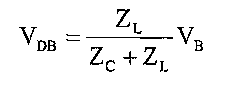
- The ratio RAB (VDA/VDB) is expressed as:

- It can be seen from the above formula that RAB shows the relationship between ratio of low-frequency sampling component to high-frequency sampling component against the frequency for the compound feedback signal. Because the change of the ratio is proportional to the square of the frequency change, the method of the invention gains a feature of rapid frequency change, thus can achieving deeper feedback depth using narrower bandwidth in low-frequency feedback sampling. This is an important feature of the double signal combining circuit of the invention.
- If the frequency at which RAB equals to 1 is defined as the crossover frequency Fs of the double sampling feedback system, then
- Referring to Fig. 2, because the inductor L1 and the capacitor C1 are dynamic elements, the frequency characteristic of compound feedback signal at point D may have fluctuation in the band that between the high and low-sampling frequency, thus resulting in instability. In order to reduce the fluctuation, the inductor L1 may connect with a damping resistor in parallel, or the capacitor C1 may connect in series with a damping resistor. In an actual application circuit, as the damping resistor connected in series with the capacitor C1 is very small, the inner resistor of the buffer could be used as the resistor in this case. In the circuit shown in Fig.3, a damping resistor R1 is added in parallel to the inductor L1. In the circuit shown in Fig.4, a damping resistor R2 is added in series with the capacitor C1. In the circuit shown in Fig.5, a damping resistor R1 in parallel to the inductor L1 and a damping resistor R2 in series with the capacitor C1 are together added therein.
- Referring to Figs. 2-5, at the amplifying signal frequency, as the impedance of the inductor L1 is very small, VA , VB and VD have almost the same voltage level, and accordingly, the current passing through the capacitor C 1 at the amplifying signal frequency is very small. That is, the capacitor C 1 has very high impedance at the amplifying signal band. At high-frequency band have only small interference and noise voltage. Therefore, the high-speed buffer circuit drives a very small current at full frequency range.
- Fig. 6 shows a block illustrating a circuit of a double sampling negative feedback amplifier in accordance with a second embodiment of the invention. Compared with the first example embodiment, the double feedback amplifying circuit further contains a high-
pass filter circuit 16 on the high-frequency sampling channel. The high-pass filter circuit 16 is used to remove the signal of the amplifying signal frequency from the high-frequency sampling channel. - Because the high-
pass filter circuit 16 is incorporated prior to the high-speed buffer circuit 13 to reduce the amplifying signal at node B, the sampling of the amplifying signal in the high-frequency channel is reduced without stability of the feedback circuit being influenced. In the invention, the high-pass filter circuit 16 can be positioned at either the input or output of the high-speed buffer circuit 13. - After the high-
pass filter circuit 16 is incorporated into the high-frequency sampling channel, at the amplifying signal frequency band, a current will pass through the capacitor C1 due to lower voltage level of VB than that of VA and VD. It will bring two problems. Firstly, the output current of the high-speed buffer circuit 13 will be increased and accordingly, the drive ability of the current need be extended. Secondly, the bypass effect of the capacitor C1 causes the signal response speed at node D less than that at node A. As a result, the response speed of the feedback signal is decreased and the dynamic performance of the amplifying circuit turns to be bad. Considering the above problems, it is necessary to have all things considered when in use. - Fig. 7 shows a block illustrating a circuit of a double sampling negative feedback amplifier in accordance with a third embodiment of the invention. Compared with the first example embodiment, a voltage gain stage, i.e., an in-phase
voltage amplifying circuit 17, is positioned prior to theoutput buffer circuit 12. The in-phasevoltage amplifying circuit 17 enhances the voltage gain at low-frequency channel such that the DC gain at low-frequency channel is higher than that at high-frequency channel, and as a result, the feedback depth of the amplifying frequency is increased. Because the gain at low-frequency channel is higher than that at high-frequency, at the amplifying signal frequency band, the signal voltage level of VB is less than VA and VD. The signal voltage level of VB is less than VA at the crossover frequency. It can be known from the expression of Fs that either the capacitor C1 or the inductor L1 should have a larger value. Thus, we can understand that the circuit has the same problem as the circuit shown in Fig.6. In addition, the response speed of the feedback signal is decreased due to larger value of the capacitor C1 and/or the inductor L1. As a result, the dynamic performance of the amplifying circuit turns to be bad. - Fig. 8 shows a block illustrating a circuit of a double sampling negative feedback amplifier in accordance with another embodiment of the invention. In the embodiment, a low-
pass filter circuit 18 is added before the low-frequency sampling channel for removing high-frequency signal from the low-frequency sampling channel. The low pass filtering decrease the response speed of the feedback signal, and thus causes the dynamic performance of the amplifying circuit turns to be bad. Notably, the low pass filtering increases the phase-shift in the low-frequency feedback loop, and undue control will influence the stability of the feedback loop. - Fig. 9 shows a block illustrating a circuit of a double sampling negative feedback amplifier in accordance with a fifth embodiment of the invention. In fact, this embodiment is just a modification of the first example embodiment, and therefore, further details thereof are omitted.
- Fig. 10 shows an actual circuit of the first embodiment of the invention. In the circuit, the
voltage amplifying circuit 11 comprises Q01, R01, Q02, R02, Q03, Q04, R04, Q05, R05, Q06, R06, Q07, R07, Q08, R08, Q09, R09, Q10, R10, Q11, R11, Q12, R12, Q13, Q14, Q15, R15, Q16, R16, Q17, Q18, W01, D01, D02, R13, D03, D04, R21. The high-speed buffer circuit 13 comprises Q19, R17, Q20, C03 and C04. Theoutput buffer circuit 12 comprises Q21, R18, Q22, Q23, R19, Q24 and R20. The doublesignal combining circuit 14 comprises C02, L01 and R14. The feedback network comprises R22 and R23. - After utilization of the invention, it will bring several advantages. Firstly, as the output buffer circuit thereafter is kept away from the high-frequency feedback loop, the stability at high-frequency will not be influenced by the output buffer circuit (stage) and changeable load, while the output buffer circuit and the load often have great impact on the feedback depth, thus the stability being affected only at low-frequency. Accordingly, the feedback depth of high-frequency is enhanced, i.e., more stable feedback depth can be obtained. Secondly, because the series capacitor-inductor double signal combining circuit has a feature of rapid frequency change, a relatively narrow bandwidth of the output buffer stage of the amplifier is sufficient to achieve deeper feedback depth, thus reducing difficulty in realizing deep negative loop feedback.
- While the invention has been described in connection with what are presently considered to be the most practical and preferred embodiments, it is to be understood that the invention is not to be limited to the disclosed embodiments, but on the contrary, is intended to cover various modifications and equivalent arrangements included within the spirit and scope of the invention.
Claims (7)
- A method for double sampling loop negative feedback, comprising the steps of:obtaining a low-frequency feedback signal from the output of the amplifier;obtaining a high-frequency feedback signal from part of the amplifier of which high-frequency phase shift is low, wherein two-ways sampling signals have the same amplifying phase;combining the two sampling signals using a series capacitor-inductor double signal combining circuit to form one signal, which having low phase shift at both high and low-frequency and being used for negative loop feedback.
- The method according to claim 1, wherein a damping resistor may be added to the capacitor-inductor in series type of double sampling-combining circuit in parallel to the inductor or in series to the capacitor, or a damping resistor may be in parallel to the inductor and another resistor may be in series to the capacitor at a time.
- A double sampling negative feedback amplifier, comprising:a voltage amplifying circuit used to output voltage signal and transfer it to a high-speed buffer circuit and an output buffer circuit;an output buffer circuit used to achieve unit voltage gain, provide amplified output signal and low-frequency feedback sampling signal for a double signal combining circuit;a high-speed buffer circuit used to achieve unit voltage gain and output high-frequency feedback sampling signal to a double signal combining circuit;a series capacitor-inductor double signal combining circuit used to combine the high and low-frequency feedback signals to form one-way compound feedback signal; anda feedback network for transfer the compound feedback signal to an inverting input of the voltage amplifying circuit.
- The double sampling negative feedback amplifier according to claim 3, wherein the double feedback amplifier has a high-pass filter circuit incorporated in its high-frequency sampling channel in order to remove the signal on the amplifying signal frequency from the high-frequency sampling channel.
- The double sampling negative feedback amplifier of claim 3, wherein the double sampling negative feedback amplifier further comprises a voltage gain stage prior to the output buffer circuit.
- The double sampling negative feedback amplifier of claim 3, wherein the double sampling negative feedback amplifier further comprises a low-pass filter circuit prior to the low-frequency sampling node for removing the high-frequency signal from the low-frequency sampling channel.
- The double sampling negative feedback amplifier of claim 3, wherein a damping resistor may be added to the series capacitor-inductor double signal combining circuit in parallel to the inductor or in series to the capacitor, or a damping resistor may be in parallel to the inductor and another resistor may be in series to the capacitor at a time.
Applications Claiming Priority (2)
| Application Number | Priority Date | Filing Date | Title |
|---|---|---|---|
| CNB2004100512468A CN100461623C (en) | 2004-08-27 | 2004-08-27 | Double-way sampling loop negative feedback method and two-way sampling negative feed back amplifier |
| PCT/CN2005/001223 WO2006021142A1 (en) | 2004-08-27 | 2005-08-10 | Method for double sampling loop negative feedback and double sampling negative feedback amplifier |
Publications (4)
| Publication Number | Publication Date |
|---|---|
| EP1788700A1 true EP1788700A1 (en) | 2007-05-23 |
| EP1788700A4 EP1788700A4 (en) | 2009-04-01 |
| EP1788700B1 EP1788700B1 (en) | 2010-11-03 |
| EP1788700B8 EP1788700B8 (en) | 2010-12-22 |
Family
ID=35967160
Family Applications (1)
| Application Number | Title | Priority Date | Filing Date |
|---|---|---|---|
| EP05774340A Expired - Lifetime EP1788700B8 (en) | 2004-08-27 | 2005-08-10 | Method for double sampling loop negative feedback and double sampling negative feedback amplifier |
Country Status (7)
| Country | Link |
|---|---|
| US (1) | US7403068B2 (en) |
| EP (1) | EP1788700B8 (en) |
| CN (1) | CN100461623C (en) |
| AT (1) | ATE487273T1 (en) |
| DE (1) | DE602005024577D1 (en) |
| RU (1) | RU2007111878A (en) |
| WO (1) | WO2006021142A1 (en) |
Cited By (1)
| Publication number | Priority date | Publication date | Assignee | Title |
|---|---|---|---|---|
| EP2575298A1 (en) | 2011-08-11 | 2013-04-03 | brainchild GmbH | Method and device for secure handling of an email message |
Families Citing this family (9)
| Publication number | Priority date | Publication date | Assignee | Title |
|---|---|---|---|---|
| WO2008106822A1 (en) * | 2007-03-06 | 2008-09-12 | Zongshan Zhou | Method for resistance combining double sampling loop negative feedback and amplifier thereof |
| TWI358220B (en) * | 2008-04-21 | 2012-02-11 | Ra Link Technology Corp | Signal transmitting apparatus for ofdm system and |
| US20090245541A1 (en) * | 2009-03-16 | 2009-10-01 | Zhenwu Wang | Audio Power Amplifier with Feedback-Shifting Technology |
| US8055212B2 (en) * | 2009-05-26 | 2011-11-08 | ST-Erisson SA | Transmitter phase shift determination and compensation |
| CN101826844B (en) | 2010-05-06 | 2012-08-08 | 华为技术有限公司 | A kind of power amplifier and signal amplification method based on power amplifier |
| CN102158179B (en) * | 2011-03-18 | 2014-04-02 | 复旦大学 | Multimode low-noise amplifier adopting positive and negative feedback structure |
| TWI732367B (en) * | 2019-12-02 | 2021-07-01 | 香港商吉達物聯科技股份有限公司 | Multi-level noise shaping system, method and non-transitory computer-readable medium |
| CN112596571A (en) * | 2020-12-15 | 2021-04-02 | 固高科技(深圳)有限公司 | Driving circuit and driving system based on double negative feedback |
| CN112653403B (en) * | 2020-12-24 | 2023-03-14 | 唯捷创芯(天津)电子技术股份有限公司 | Radio frequency power amplifier, chip and communication terminal for reducing load change sensitivity |
Family Cites Families (14)
| Publication number | Priority date | Publication date | Assignee | Title |
|---|---|---|---|---|
| US3813609A (en) * | 1972-11-27 | 1974-05-28 | Petty Ray Geophysical Inc | Multiple stage sample normalizing amplifier with automatic gain prediction |
| JPS6134749Y2 (en) * | 1979-09-28 | 1986-10-09 | ||
| DE3036887C2 (en) * | 1980-09-30 | 1982-10-28 | Siemens AG, 1000 Berlin und 8000 München | Negative feedback circuit arrangement for a transistor amplifier, in particular an integrated transistor amplifier |
| US4470020A (en) * | 1982-05-06 | 1984-09-04 | Mohr Daniel R | Virtual ground preamplifier for magnetic phono cartridge |
| US4481480A (en) * | 1982-10-04 | 1984-11-06 | Tektronix, Inc. | Feedback amplifier having a voltage-controlled compensation circuit |
| US4634993A (en) * | 1985-08-23 | 1987-01-06 | Burr-Brown Corporation | High gain, low drift operational amplifier for sample and hold circuit |
| CN2081605U (en) * | 1990-06-15 | 1991-07-24 | 陈国伟 | Class ab bridge amplifier |
| GB2293935B (en) * | 1994-10-03 | 1999-07-14 | Linear Modulation Tech | Automatic calibration of carrier suppression and loop phase in a cartesian amplifier |
| US6081158A (en) * | 1997-06-30 | 2000-06-27 | Harris Corporation | Adaptive pre-distortion apparatus for linearizing an amplifier output within a data transmission system |
| US5974089A (en) * | 1997-07-22 | 1999-10-26 | Tripath Technology, Inc. | Method and apparatus for performance improvement by qualifying pulses in an oversampled noise-shaping signal processor |
| US6175276B1 (en) * | 1998-03-16 | 2001-01-16 | National Semiconductor Corporation | Indirect emitter-coupling preamplifier for magneto-resistive heads with single-ended feedback |
| CN2388776Y (en) | 1999-03-19 | 2000-07-19 | 桂杰 | Transistor loopless negative feedback power amplifier |
| US7061313B2 (en) * | 2000-05-05 | 2006-06-13 | Telefonaktiebolaget Lm Ericsson (Publ) | Dual feedback linear amplifier |
| US6417504B1 (en) * | 2000-09-29 | 2002-07-09 | Innovative Technology Licensing, Llc | Compact ultra-low noise high-bandwidth pixel amplifier for single-photon readout of photodetectors |
-
2004
- 2004-08-27 CN CNB2004100512468A patent/CN100461623C/en not_active Expired - Fee Related
-
2005
- 2005-08-10 AT AT05774340T patent/ATE487273T1/en not_active IP Right Cessation
- 2005-08-10 EP EP05774340A patent/EP1788700B8/en not_active Expired - Lifetime
- 2005-08-10 DE DE602005024577T patent/DE602005024577D1/en not_active Expired - Lifetime
- 2005-08-10 RU RU2007111878/09A patent/RU2007111878A/en not_active Application Discontinuation
- 2005-08-10 WO PCT/CN2005/001223 patent/WO2006021142A1/en not_active Ceased
- 2005-08-10 US US11/574,383 patent/US7403068B2/en not_active Expired - Fee Related
Cited By (1)
| Publication number | Priority date | Publication date | Assignee | Title |
|---|---|---|---|---|
| EP2575298A1 (en) | 2011-08-11 | 2013-04-03 | brainchild GmbH | Method and device for secure handling of an email message |
Also Published As
| Publication number | Publication date |
|---|---|
| ATE487273T1 (en) | 2010-11-15 |
| WO2006021142A1 (en) | 2006-03-02 |
| CN100461623C (en) | 2009-02-11 |
| RU2007111878A (en) | 2008-10-10 |
| EP1788700A4 (en) | 2009-04-01 |
| EP1788700B1 (en) | 2010-11-03 |
| CN1741371A (en) | 2006-03-01 |
| US20070296502A1 (en) | 2007-12-27 |
| EP1788700B8 (en) | 2010-12-22 |
| DE602005024577D1 (en) | 2010-12-16 |
| US7403068B2 (en) | 2008-07-22 |
Similar Documents
| Publication | Publication Date | Title |
|---|---|---|
| JP3174340B2 (en) | Automatic gain control device for receiver | |
| EP1788700B1 (en) | Method for double sampling loop negative feedback and double sampling negative feedback amplifier | |
| US5982232A (en) | Low noise, bandwidth compensated transimpedance amplifier | |
| GB1577467A (en) | Microwave signal amplifiers | |
| CA1296397C (en) | Automatic gain control amplifier for compensating cable loss | |
| JP2561025B2 (en) | Unbalance-balance conversion circuit | |
| CN115053453A (en) | Feedforward amplifying circuit, audio amplifier and audio playing device | |
| US4491689A (en) | Amplifier for use with telephone transmitter mounted in hand held telephone unit | |
| JP2007150434A (en) | Analog amplifier and transmitter / receiver using the same | |
| JPS61196625A (en) | Autodyne receiver | |
| US3980967A (en) | Differential feedback amplifier with frequency-shaped reference signal | |
| JP3403387B2 (en) | Transmission device | |
| JP3097740B2 (en) | Audio signal recording compensator | |
| JP3394116B2 (en) | Power supply ripple suppression circuit for differential amplifier | |
| US20240014791A1 (en) | Amplifier system | |
| KR100334889B1 (en) | Multi-combination linear power amplifier | |
| JP3917571B2 (en) | Differential circuit and transconductor using it | |
| JP2002359525A (en) | Audio power amplifying circuit | |
| JP2005236866A (en) | High frequency power amplifier | |
| JPH08167815A (en) | Negative feedback amplifier | |
| JP3234479B2 (en) | FM detection circuit | |
| JPH0618307B2 (en) | Operational amplifier | |
| JPS5850444B2 (en) | auto-balanced amplifier circuit | |
| Self | Microphone preamplifiers | |
| JPS58162109A (en) | Power amplifier |
Legal Events
| Date | Code | Title | Description |
|---|---|---|---|
| PUAI | Public reference made under article 153(3) epc to a published international application that has entered the european phase |
Free format text: ORIGINAL CODE: 0009012 |
|
| 17P | Request for examination filed |
Effective date: 20070326 |
|
| AK | Designated contracting states |
Kind code of ref document: A1 Designated state(s): AT BE BG CH CY CZ DE DK EE ES FI FR GB GR HU IE IS IT LI LT LU LV MC NL PL PT RO SE SI SK TR |
|
| DAX | Request for extension of the european patent (deleted) | ||
| A4 | Supplementary search report drawn up and despatched |
Effective date: 20090226 |
|
| 17Q | First examination report despatched |
Effective date: 20090423 |
|
| GRAP | Despatch of communication of intention to grant a patent |
Free format text: ORIGINAL CODE: EPIDOSNIGR1 |
|
| GRAS | Grant fee paid |
Free format text: ORIGINAL CODE: EPIDOSNIGR3 |
|
| GRAA | (expected) grant |
Free format text: ORIGINAL CODE: 0009210 |
|
| RAP1 | Party data changed (applicant data changed or rights of an application transferred) |
Owner name: ZHOU, ZONGSHAN |
|
| RIN1 | Information on inventor provided before grant (corrected) |
Inventor name: ZHOU, ZONGSHAN |
|
| AK | Designated contracting states |
Kind code of ref document: B1 Designated state(s): AT BE BG CH CY CZ DE DK EE ES FI FR GB GR HU IE IS IT LI LT LU LV MC NL PL PT RO SE SI SK TR |
|
| REG | Reference to a national code |
Ref country code: GB Ref legal event code: FG4D |
|
| REG | Reference to a national code |
Ref country code: CH Ref legal event code: EP |
|
| REG | Reference to a national code |
Ref country code: IE Ref legal event code: FG4D |
|
| REF | Corresponds to: |
Ref document number: 602005024577 Country of ref document: DE Date of ref document: 20101216 Kind code of ref document: P |
|
| REG | Reference to a national code |
Ref country code: NL Ref legal event code: VDEP Effective date: 20101103 |
|
| LTIE | Lt: invalidation of european patent or patent extension |
Effective date: 20101103 |
|
| PG25 | Lapsed in a contracting state [announced via postgrant information from national office to epo] |
Ref country code: LT Free format text: LAPSE BECAUSE OF FAILURE TO SUBMIT A TRANSLATION OF THE DESCRIPTION OR TO PAY THE FEE WITHIN THE PRESCRIBED TIME-LIMIT Effective date: 20101103 |
|
| PG25 | Lapsed in a contracting state [announced via postgrant information from national office to epo] |
Ref country code: NL Free format text: LAPSE BECAUSE OF FAILURE TO SUBMIT A TRANSLATION OF THE DESCRIPTION OR TO PAY THE FEE WITHIN THE PRESCRIBED TIME-LIMIT Effective date: 20101103 Ref country code: IS Free format text: LAPSE BECAUSE OF FAILURE TO SUBMIT A TRANSLATION OF THE DESCRIPTION OR TO PAY THE FEE WITHIN THE PRESCRIBED TIME-LIMIT Effective date: 20110303 Ref country code: LV Free format text: LAPSE BECAUSE OF FAILURE TO SUBMIT A TRANSLATION OF THE DESCRIPTION OR TO PAY THE FEE WITHIN THE PRESCRIBED TIME-LIMIT Effective date: 20101103 Ref country code: SE Free format text: LAPSE BECAUSE OF FAILURE TO SUBMIT A TRANSLATION OF THE DESCRIPTION OR TO PAY THE FEE WITHIN THE PRESCRIBED TIME-LIMIT Effective date: 20101103 Ref country code: BG Free format text: LAPSE BECAUSE OF FAILURE TO SUBMIT A TRANSLATION OF THE DESCRIPTION OR TO PAY THE FEE WITHIN THE PRESCRIBED TIME-LIMIT Effective date: 20110203 Ref country code: PT Free format text: LAPSE BECAUSE OF FAILURE TO SUBMIT A TRANSLATION OF THE DESCRIPTION OR TO PAY THE FEE WITHIN THE PRESCRIBED TIME-LIMIT Effective date: 20110303 Ref country code: SI Free format text: LAPSE BECAUSE OF FAILURE TO SUBMIT A TRANSLATION OF THE DESCRIPTION OR TO PAY THE FEE WITHIN THE PRESCRIBED TIME-LIMIT Effective date: 20101103 Ref country code: FI Free format text: LAPSE BECAUSE OF FAILURE TO SUBMIT A TRANSLATION OF THE DESCRIPTION OR TO PAY THE FEE WITHIN THE PRESCRIBED TIME-LIMIT Effective date: 20101103 Ref country code: AT Free format text: LAPSE BECAUSE OF FAILURE TO SUBMIT A TRANSLATION OF THE DESCRIPTION OR TO PAY THE FEE WITHIN THE PRESCRIBED TIME-LIMIT Effective date: 20101103 |
|
| PG25 | Lapsed in a contracting state [announced via postgrant information from national office to epo] |
Ref country code: GR Free format text: LAPSE BECAUSE OF FAILURE TO SUBMIT A TRANSLATION OF THE DESCRIPTION OR TO PAY THE FEE WITHIN THE PRESCRIBED TIME-LIMIT Effective date: 20110204 |
|
| PG25 | Lapsed in a contracting state [announced via postgrant information from national office to epo] |
Ref country code: BE Free format text: LAPSE BECAUSE OF FAILURE TO SUBMIT A TRANSLATION OF THE DESCRIPTION OR TO PAY THE FEE WITHIN THE PRESCRIBED TIME-LIMIT Effective date: 20101103 Ref country code: ES Free format text: LAPSE BECAUSE OF FAILURE TO SUBMIT A TRANSLATION OF THE DESCRIPTION OR TO PAY THE FEE WITHIN THE PRESCRIBED TIME-LIMIT Effective date: 20110214 Ref country code: EE Free format text: LAPSE BECAUSE OF FAILURE TO SUBMIT A TRANSLATION OF THE DESCRIPTION OR TO PAY THE FEE WITHIN THE PRESCRIBED TIME-LIMIT Effective date: 20101103 Ref country code: CZ Free format text: LAPSE BECAUSE OF FAILURE TO SUBMIT A TRANSLATION OF THE DESCRIPTION OR TO PAY THE FEE WITHIN THE PRESCRIBED TIME-LIMIT Effective date: 20101103 |
|
| PG25 | Lapsed in a contracting state [announced via postgrant information from national office to epo] |
Ref country code: PL Free format text: LAPSE BECAUSE OF FAILURE TO SUBMIT A TRANSLATION OF THE DESCRIPTION OR TO PAY THE FEE WITHIN THE PRESCRIBED TIME-LIMIT Effective date: 20101103 Ref country code: RO Free format text: LAPSE BECAUSE OF FAILURE TO SUBMIT A TRANSLATION OF THE DESCRIPTION OR TO PAY THE FEE WITHIN THE PRESCRIBED TIME-LIMIT Effective date: 20101103 Ref country code: DK Free format text: LAPSE BECAUSE OF FAILURE TO SUBMIT A TRANSLATION OF THE DESCRIPTION OR TO PAY THE FEE WITHIN THE PRESCRIBED TIME-LIMIT Effective date: 20101103 Ref country code: SK Free format text: LAPSE BECAUSE OF FAILURE TO SUBMIT A TRANSLATION OF THE DESCRIPTION OR TO PAY THE FEE WITHIN THE PRESCRIBED TIME-LIMIT Effective date: 20101103 |
|
| PLBE | No opposition filed within time limit |
Free format text: ORIGINAL CODE: 0009261 |
|
| STAA | Information on the status of an ep patent application or granted ep patent |
Free format text: STATUS: NO OPPOSITION FILED WITHIN TIME LIMIT |
|
| 26N | No opposition filed |
Effective date: 20110804 |
|
| REG | Reference to a national code |
Ref country code: DE Ref legal event code: R097 Ref document number: 602005024577 Country of ref document: DE Effective date: 20110804 |
|
| PG25 | Lapsed in a contracting state [announced via postgrant information from national office to epo] |
Ref country code: IT Free format text: LAPSE BECAUSE OF FAILURE TO SUBMIT A TRANSLATION OF THE DESCRIPTION OR TO PAY THE FEE WITHIN THE PRESCRIBED TIME-LIMIT Effective date: 20101103 |
|
| PG25 | Lapsed in a contracting state [announced via postgrant information from national office to epo] |
Ref country code: MC Free format text: LAPSE BECAUSE OF NON-PAYMENT OF DUE FEES Effective date: 20110831 |
|
| REG | Reference to a national code |
Ref country code: CH Ref legal event code: PL |
|
| GBPC | Gb: european patent ceased through non-payment of renewal fee |
Effective date: 20110810 |
|
| PG25 | Lapsed in a contracting state [announced via postgrant information from national office to epo] |
Ref country code: CH Free format text: LAPSE BECAUSE OF NON-PAYMENT OF DUE FEES Effective date: 20110831 Ref country code: LI Free format text: LAPSE BECAUSE OF NON-PAYMENT OF DUE FEES Effective date: 20110831 |
|
| REG | Reference to a national code |
Ref country code: FR Ref legal event code: ST Effective date: 20120430 |
|
| REG | Reference to a national code |
Ref country code: IE Ref legal event code: MM4A |
|
| REG | Reference to a national code |
Ref country code: DE Ref legal event code: R119 Ref document number: 602005024577 Country of ref document: DE Effective date: 20120301 |
|
| PG25 | Lapsed in a contracting state [announced via postgrant information from national office to epo] |
Ref country code: IE Free format text: LAPSE BECAUSE OF NON-PAYMENT OF DUE FEES Effective date: 20110810 |
|
| PG25 | Lapsed in a contracting state [announced via postgrant information from national office to epo] |
Ref country code: GB Free format text: LAPSE BECAUSE OF NON-PAYMENT OF DUE FEES Effective date: 20110810 Ref country code: FR Free format text: LAPSE BECAUSE OF NON-PAYMENT OF DUE FEES Effective date: 20110831 |
|
| PG25 | Lapsed in a contracting state [announced via postgrant information from national office to epo] |
Ref country code: LU Free format text: LAPSE BECAUSE OF NON-PAYMENT OF DUE FEES Effective date: 20110810 Ref country code: CY Free format text: LAPSE BECAUSE OF EXPIRATION OF PROTECTION Effective date: 20101103 |
|
| PG25 | Lapsed in a contracting state [announced via postgrant information from national office to epo] |
Ref country code: DE Free format text: LAPSE BECAUSE OF NON-PAYMENT OF DUE FEES Effective date: 20120301 |
|
| PG25 | Lapsed in a contracting state [announced via postgrant information from national office to epo] |
Ref country code: TR Free format text: LAPSE BECAUSE OF FAILURE TO SUBMIT A TRANSLATION OF THE DESCRIPTION OR TO PAY THE FEE WITHIN THE PRESCRIBED TIME-LIMIT Effective date: 20101103 |
|
| PG25 | Lapsed in a contracting state [announced via postgrant information from national office to epo] |
Ref country code: HU Free format text: LAPSE BECAUSE OF FAILURE TO SUBMIT A TRANSLATION OF THE DESCRIPTION OR TO PAY THE FEE WITHIN THE PRESCRIBED TIME-LIMIT Effective date: 20101103 |