EP1788629A1 - A readout chip for single photon counting - Google Patents
A readout chip for single photon counting Download PDFInfo
- Publication number
- EP1788629A1 EP1788629A1 EP05025326A EP05025326A EP1788629A1 EP 1788629 A1 EP1788629 A1 EP 1788629A1 EP 05025326 A EP05025326 A EP 05025326A EP 05025326 A EP05025326 A EP 05025326A EP 1788629 A1 EP1788629 A1 EP 1788629A1
- Authority
- EP
- European Patent Office
- Prior art keywords
- counter
- shift register
- readout
- bits
- data
- Prior art date
- Legal status (The legal status is an assumption and is not a legal conclusion. Google has not performed a legal analysis and makes no representation as to the accuracy of the status listed.)
- Withdrawn
Links
- 238000003384 imaging method Methods 0.000 abstract description 7
- 238000005513 bias potential Methods 0.000 description 4
- 239000000523 sample Substances 0.000 description 4
- 239000013078 crystal Substances 0.000 description 3
- 238000012986 modification Methods 0.000 description 3
- 230000004048 modification Effects 0.000 description 3
- 238000006243 chemical reaction Methods 0.000 description 2
- 238000002050 diffraction method Methods 0.000 description 2
- 238000002474 experimental method Methods 0.000 description 2
- 239000000463 material Substances 0.000 description 2
- 238000012544 monitoring process Methods 0.000 description 2
- 239000000843 powder Substances 0.000 description 2
- 230000005469 synchrotron radiation Effects 0.000 description 2
- 230000036962 time dependent Effects 0.000 description 2
- 238000002441 X-ray diffraction Methods 0.000 description 1
- 238000004458 analytical method Methods 0.000 description 1
- 230000007547 defect Effects 0.000 description 1
- 230000004907 flux Effects 0.000 description 1
- 238000011835 investigation Methods 0.000 description 1
- 239000011159 matrix material Substances 0.000 description 1
- 239000011368 organic material Substances 0.000 description 1
- 238000012545 processing Methods 0.000 description 1
- 102000004169 proteins and genes Human genes 0.000 description 1
- 108090000623 proteins and genes Proteins 0.000 description 1
- 230000005855 radiation Effects 0.000 description 1
Images
Classifications
-
- H—ELECTRICITY
- H01—ELECTRIC ELEMENTS
- H01L—SEMICONDUCTOR DEVICES NOT COVERED BY CLASS H10
- H01L27/00—Devices consisting of a plurality of semiconductor or other solid-state components formed in or on a common substrate
- H01L27/14—Devices consisting of a plurality of semiconductor or other solid-state components formed in or on a common substrate including semiconductor components sensitive to infrared radiation, light, electromagnetic radiation of shorter wavelength or corpuscular radiation and specially adapted either for the conversion of the energy of such radiation into electrical energy or for the control of electrical energy by such radiation
- H01L27/144—Devices controlled by radiation
- H01L27/1446—Devices controlled by radiation in a repetitive configuration
-
- H—ELECTRICITY
- H01—ELECTRIC ELEMENTS
- H01L—SEMICONDUCTOR DEVICES NOT COVERED BY CLASS H10
- H01L31/00—Semiconductor devices sensitive to infrared radiation, light, electromagnetic radiation of shorter wavelength or corpuscular radiation and specially adapted either for the conversion of the energy of such radiation into electrical energy or for the control of electrical energy by such radiation; Processes or apparatus specially adapted for the manufacture or treatment thereof or of parts thereof; Details thereof
- H01L31/08—Semiconductor devices sensitive to infrared radiation, light, electromagnetic radiation of shorter wavelength or corpuscular radiation and specially adapted either for the conversion of the energy of such radiation into electrical energy or for the control of electrical energy by such radiation; Processes or apparatus specially adapted for the manufacture or treatment thereof or of parts thereof; Details thereof in which radiation controls flow of current through the device, e.g. photoresistors
- H01L31/10—Semiconductor devices sensitive to infrared radiation, light, electromagnetic radiation of shorter wavelength or corpuscular radiation and specially adapted either for the conversion of the energy of such radiation into electrical energy or for the control of electrical energy by such radiation; Processes or apparatus specially adapted for the manufacture or treatment thereof or of parts thereof; Details thereof in which radiation controls flow of current through the device, e.g. photoresistors characterised by at least one potential-jump barrier or surface barrier, e.g. phototransistors
- H01L31/101—Devices sensitive to infrared, visible or ultraviolet radiation
Definitions
- the present invention relates to a readout chip for single photon counting.
- X-ray diffraction patterns are useful in the analysis of both organic and inorganic crystallographic structures.
- organic materials such as protein crystals
- x-ray detectors particularly where the x-ray source is high flux synchrotron radiation that enables and requires, due to the radiation damage, an experiment to be done rapidly.
- synchrotron radiation such as crystallography and/or powder diffraction analysis.
- Monitoring a time-dependent reaction in a sample i.e. a crystal or a powder, can elucidate the time-dependent crystal/molecular changes that occur in a chemical reaction. High time resolution is often critical in such monitoring.
- a fast single photon-counting imaging device for the above-mentioned purposes has been disclosed in the international patent application WO 2004/064168 .
- This reference teaches in detail a photon-counting imaging device for single x-ray counting which comprises:
- a photon counting imaging device having an architecture of the readout circuitry that allows to be tolerant with respect to a local defect of a detector diode and/or readout unit cell and that allows to control and redesign the program and/or the status of each detector diode and/or readout unit cell in order to achieve a fast photon counting imaging device.
- a readout chip for single photon counting which comprises:
- the data input shift register, the data output shift register as well as the channel select shift register and the counters comprise a CLEAR and a SET CONTROL signal which allows to clear and set the registers within one cycle per signal.
- the control signals are multiplexed to the data input-, data output- and channel select shift registers as well as the counter.
- the signals needed for the redout are also available non multiplexed in order not to compromise the readout speed.
- the programmable bits can be used for a DAC, i.e. for fine-tuning of a comparator threshold, enabling/disabling of a calibration pulse, for enabling/disabling the analogue output of a channel and for enabling the output of the channels comparator.
- the data input shift register and the data output shift register may have at least the length of the counter.
- the data input shift register has additionally a number of bits for the programmable bits which are used as explained above.
- the length of the counter may be an odd or an even multiple of the number K of the data outputs. According to the value of the multiple a respective number of integer cycles is used to read out the complete data output shift register. For example, assuming a 24 bit binary counter and a 4 bit parallel data output, six cycles for reading the 24 bit string counting value plus three cycles for selecting, controlling and resetting the data output shift register are required to readout the counter value of one channel. In case only four bits are necessary to be read out, like the four minor important bits 0 through 3, only 4 cycles are required in total. These features allow to cut down the readout time by more than 50% for those "channels of minor interest" (lower counting rates).
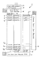
- the figure depicts a schematic view on the architecture of a readout chip 2 for use in a photon-counting imaging device.
- the readout chip 2 comprises a data input shift register 4 having a length of 33 bits. 24 bits of the data input shift register 4 is associated with a 24 bit data input bus 6 which connects to selectable counters 8 1 to 8 128 . The remaining nine bits of the data input shift register 4 are associated via a 9-bit data input bus 10 with the programmable bits pb1 to pb128 of each of the 128 channels. For selecting the channel, a channel select shift register 12 is provided.
- the programmable bits pb1 to pb128 are used for example for enabling/disabling the respective channel, for forwarding the analogue signal (which reflects the number and energy of the incident photons on each diode) to the analogue output of the chip (i.e. for calibration and debugging purposes), other bits are used for programming the DAC (6 bits), for fine-tuning of the comparator threshold, for enabling/disabling of a calibration pulse etc.
- the counter 8 1 to 8 128 are selectively connectable via a 24-bit data output bus 14 to a data output shift register 16.
- a multiplexer 18 the 24 bits of the data output shift register can be selectively assigned to a 4-bit data output 20 which allows in the present example to readout in parallel four selectable bits of the data output shift register 16.
- the multiplexer in the present example, is controlled by bits of the data input shift register.
- all the registers 4, 12, 8 1-128 and 16 comprise a leg for a CLEAR and a SET CONTROL signal.
- These control signals are further multiplexed which means that the number of control signals is reduced while further simplifying the operation. This can be done for example by mode multiplexing of the respective control signals.
- Another preferred modification may propose a data output 20 having more than 4 bits up to the maximal length of the counter 8 1 to 8 128 which would allow to readout the counter much faster and in parallel mode in case of the same length for both the counter and the data output within only one cycle (plus control signal cycles).
- the counter of a distinct channel can be set to an arbitrary value.
- the values for the programmable bits and the counter value can be entered into the readout chip 2 by the serial data input shift register 4 which could be also be a parallel data input register for the complete length of the counters.
- the input shift register also serves to program the multiplexer for the data output.
Abstract
It is the aim of the present invention to improve the properties and the speed of readout electronic significantly without losing accuracy of the counting in photon-counting imaging devices.
This aim is achieved according to the present invention by a readout chip (2) for single photon counting, comprising:
a) a plurality of N individually working channels each assigned to a respective detector diode; each channel comprising a counter (81 to 8128) being designed as a binary counter having a length of M bits and a number of programmable bits (pb1 to pb128);
b) a serial or parallel data input shift register (4) for entering values for the counter (81 to 8128) and the programmable bits (pb1 to pb128); and
c) a number of data output shift register (16); each having a number of K data outputs (20), whereby means (18) are provided for selectively multiplexing each of the K data outputs (20) onto a selectable bit of the data output shift register (16).
These features allow a much faster readout of the counter since the counter can be readout in parallel groups of K bits each cycle. Further, a variable length of selectable bits for each counter in each channel can be readout advantageously by multiplexing the K data outputs to the bits of interest which increases the speed of readout tremendeously.
Description
- The present invention relates to a readout chip for single photon counting.
- X-ray diffraction patterns are useful in the analysis of both organic and inorganic crystallographic structures. Especially organic materials, such as protein crystals, impose stringent requirements on x-ray detectors, particularly where the x-ray source is high flux synchrotron radiation that enables and requires, due to the radiation damage, an experiment to be done rapidly. Furthermore, an important and developing field is time-resolved diffraction experiments using synchrotron radiation, such as crystallography and/or powder diffraction analysis. Monitoring a time-dependent reaction in a sample, i.e. a crystal or a powder, can elucidate the time-dependent crystal/molecular changes that occur in a chemical reaction. High time resolution is often critical in such monitoring.
- A fast single photon-counting imaging device for the above-mentioned purposes has been disclosed in the international patent application
WO 2004/064168 . This reference teaches in detail a photon-counting imaging device for single x-ray counting which comprises: - a) a layer of photosensitive material;
- b) a source of bias potential;
- c) a source of threshold voltage supply;
- d) an NxM array of photodetector diodes arranged in said layer of photosensitive material; each of said photodetector diodes having a bias potential interface and a diode output interface, said bias potential interface of each photodetector diode being connected to said bias potential;
- e) an NxM array of high gain, low noise readout unit cells, one readout unit cell for each photodetector diode;
- f) each readout unit cell comprising an input interface connected to said diode output interface, a high-gain voltage amplifying means comprising a comparator unit, a digital counter unit, comprising a digital counter, and a digital counter output interface connected in series, each digital counter unit counting an output signal of the comparator unit; said digital counter output signal is proportional to the number of absorped incident photons in the respective photodetector diode,
- g) a multiplexing means comprising a row select and a column select allowing to access each of the readout cell units, i.e. to read out the digital data as actually stored in the digital counter to the digital counter output interface;
- h) each digital counter output interface connected to an output bus;
- i) said output bus being connected to a data processing means controlling the multiplexing means.
- According to these measures, a photon counting imaging device is created having an architecture of the readout circuitry that allows to be tolerant with respect to a local defect of a detector diode and/or readout unit cell and that allows to control and redesign the program and/or the status of each detector diode and/or readout unit cell in order to achieve a fast photon counting imaging device.
- However, even for this fast photon counting imaging device it is desirable to increase the speed of the data readout. So far, the counter in the reference cited above has been designed as a pseudo-random counter, such as an 18 bit shift register with an XOR feedback. The data from this counter is serially transmitted on one digital output pin during readout. For an 18 bit shift register a readout time of at least 1+18+1 cycles is required.
- Therefore, it is the aim of the present invention to improve the properties and the speed of readout electronic significantly without losing accuracy of the counting.
- This aim is achieved according to the present invention by a readout chip for single photon counting which comprises:
- a) a plurality of N individually working channels each assigned to a respective detector diode; each channel comprising a counter being designed as a binary counter having a length of M bits and a number of programmable bits;
- b) a serial shift register or parallel data input register for entering values for the counter and the programmable bits; the binary counter enables a variable length readout since for a low number of counts not all bits have to be read out (in contrast to e.g. a pseudo random counter realized as a shift register with an X-or feedback) and
- c) a number of data output shift register; each having a number of K data outputs, whereby means are provided for selectively multiplexing each of the K data outputs onto a selectable bit of the data output shift register.
- These features allow a much faster readout of the counter since the counter can be readout in parallel groups of K bits. Further, for each counter in each channel only a variable length of selectable bits can be readout by multiplexing the K data outputs to the bits of interest which increases the readout speed tremendeously, i.e. considering in crystallographic investigations some rare regions with higher counting rates and the gross part of regions with comparably low counting rates due to the regular lattice structure of the probe.
- In order to further speed up the operation, the data input shift register, the data output shift register as well as the channel select shift register and the counters comprise a CLEAR and a SET CONTROL signal which allows to clear and set the registers within one cycle per signal. To simplify the generation of control signals and to reduce their number the control signals are multiplexed to the data input-, data output- and channel select shift registers as well as the counter. However the signals needed for the redout are also available non multiplexed in order not to compromise the readout speed.
- In order to be able to interfere with the analogue part of the readout electronic, the programmable bits can be used for a DAC, i.e. for fine-tuning of a comparator threshold, enabling/disabling of a calibration pulse, for enabling/disabling the analogue output of a channel and for enabling the output of the channels comparator.
- In a preferred embodiment of the present invention, the data input shift register and the data output shift register may have at least the length of the counter. Preferably, the data input shift register has additionally a number of bits for the programmable bits which are used as explained above. Of course, the length of the counter may be an odd or an even multiple of the number K of the data outputs. According to the value of the multiple a respective number of integer cycles is used to read out the complete data output shift register. For example, assuming a 24 bit binary counter and a 4 bit parallel data output, six cycles for reading the 24 bit string counting value plus three cycles for selecting, controlling and resetting the data output shift register are required to readout the counter value of one channel. In case only four bits are necessary to be read out, like the four minor important bits 0 through 3, only 4 cycles are required in total. These features allow to cut down the readout time by more than 50% for those "channels of minor interest" (lower counting rates).
- Further advantageous features of the preferred embodiments of the present invention can be learned from the other depending claims.
- Examples of the present invention will be described in detail with reference to the following drawing. The figure depicts a schematic view on the architecture of a
readout chip 2 for use in a photon-counting imaging device. In the present example, thereadout chip 2 comprises a datainput shift register 4 having a length of 33 bits. 24 bits of the datainput shift register 4 is associated with a 24 bitdata input bus 6 which connects to selectable counters 81 to 8128. The remaining nine bits of the datainput shift register 4 are associated via a 9-bitdata input bus 10 with the programmable bits pb1 to pb128 of each of the 128 channels. For selecting the channel, a channelselect shift register 12 is provided. The programmable bits pb1 to pb128 are used for example for enabling/disabling the respective channel, for forwarding the analogue signal (which reflects the number and energy of the incident photons on each diode) to the analogue output of the chip (i.e. for calibration and debugging purposes), other bits are used for programming the DAC (6 bits), for fine-tuning of the comparator threshold, for enabling/disabling of a calibration pulse etc. - The counter 81 to 8128 are selectively connectable via a 24-bit
data output bus 14 to a dataoutput shift register 16. By amultiplexer 18 the 24 bits of the data output shift register can be selectively assigned to a 4-bit data output 20 which allows in the present example to readout in parallel four selectable bits of the dataoutput shift register 16. The multiplexer, in the present example, is controlled by bits of the data input shift register. Considering exemplarily the diffraction pattern of a probe having a regular crystalline lattice, most of the channels will have comparably small counting rates where a readout of 4 or 8 bits appear to be sufficient for these channels; only those channels having positions corresponding to the lattice structure of the probe will receive significantly higher counting rates which will lead to the readout of all 24 bits of the counter of the respective channels. In order to further speed up the operation, all theregisters - The example shown in the drawing comprises a basic layout of the
readout chip 2 which also allows various modifications. One preferred modification can be the multiplication of the architecture with respect to the dataoutput shift register 16 for which several data output shift register could be provided. This feature enables a readout of several channels simultaneously, for example a second data output shift register enables the set-up to readout 2 X 64 channels instead of 1X 128 channels. The channels could also be organized as a 2 dimensional matrix (e.g. for 2-dimensional detectors). - Another preferred modification may propose a
data output 20 having more than 4 bits up to the maximal length of the counter 81 to 8128 which would allow to readout the counter much faster and in parallel mode in case of the same length for both the counter and the data output within only one cycle (plus control signal cycles). - The counter of a distinct channel can be set to an arbitrary value. The values for the programmable bits and the counter value can be entered into the
readout chip 2 by the serial datainput shift register 4 which could be also be a parallel data input register for the complete length of the counters. The input shift register also serves to program the multiplexer for the data output.
Claims (6)
- A readout chip (2) for single photon counting, comprising:a) a plurality of N individually working channels each assigned to a respective detector diode; each channel comprising a counter (81 to 8128) being designed as a binary counter having a length of M bits and a number of programmable bits (pb1 to pb128);b) a serial shift register or parallel data input register (4) for entering values for the counter (81 to 8128) and the programmable bits (pb1 to pb128); andc) a number of data output shift register (16); each having a number of K data outputs (20), whereby means (18) are provided for selectively multiplexing each of the K data outputs (20) onto a selectable bit of the data output shift register (16).
- The readout chip (2) according to claim 1, wherein the data input shift register (4) and the data output shift register (16) as well as a channel select shift register (12) and counter (8) comprise a CLEAR and a SET CONTROL signal leg.
- The readout chip (2) according to claim 1 or 2, wherein control signals are multiplexed and the ones needed for the readout are also available non multiplexed.
- The readout chip (2) according to anyone of the preceding claims, wherein the programmable bits (pb1 to pb128) are used for a DAC, i.e. for fine-tuning of a comparator threshold, enabling/disabling of a calibration pulse, for enabling/disabling the analogue output of a channel and for enabling the output of the channels comparator.
- The readout chip (2) according to anyone of the preceding claims, wherein the data input shift register (4) and the data output shift register (16) have at least the length of the counter (81 to 8128).
- The readout chip (2) according to anyone of the preceding claims, wherein the length of the counter (81 to 8128) is an odd or an even multiple of the number K of the data outputs (20).
Priority Applications (6)
| Application Number | Priority Date | Filing Date | Title |
|---|---|---|---|
| EP05025326A EP1788629A1 (en) | 2005-11-21 | 2005-11-21 | A readout chip for single photon counting |
| PCT/EP2006/011098 WO2007057213A1 (en) | 2005-11-21 | 2006-11-20 | A readout chip for single photon counting |
| JP2008540528A JP5078902B2 (en) | 2005-11-21 | 2006-11-20 | Readout chip for single photon counting |
| US12/085,337 US8039784B2 (en) | 2005-11-21 | 2006-11-20 | Readout chip with binary counter for fast single photon counting |
| AU2006314714A AU2006314714B2 (en) | 2005-11-21 | 2006-11-20 | A readout chip for single photon counting |
| EP06818665.9A EP1952442B1 (en) | 2005-11-21 | 2006-11-20 | A readout chip for single photon counting |
Applications Claiming Priority (1)
| Application Number | Priority Date | Filing Date | Title |
|---|---|---|---|
| EP05025326A EP1788629A1 (en) | 2005-11-21 | 2005-11-21 | A readout chip for single photon counting |
Publications (1)
| Publication Number | Publication Date |
|---|---|
| EP1788629A1 true EP1788629A1 (en) | 2007-05-23 |
Family
ID=36123312
Family Applications (2)
| Application Number | Title | Priority Date | Filing Date |
|---|---|---|---|
| EP05025326A Withdrawn EP1788629A1 (en) | 2005-11-21 | 2005-11-21 | A readout chip for single photon counting |
| EP06818665.9A Active EP1952442B1 (en) | 2005-11-21 | 2006-11-20 | A readout chip for single photon counting |
Family Applications After (1)
| Application Number | Title | Priority Date | Filing Date |
|---|---|---|---|
| EP06818665.9A Active EP1952442B1 (en) | 2005-11-21 | 2006-11-20 | A readout chip for single photon counting |
Country Status (5)
| Country | Link |
|---|---|
| US (1) | US8039784B2 (en) |
| EP (2) | EP1788629A1 (en) |
| JP (1) | JP5078902B2 (en) |
| AU (1) | AU2006314714B2 (en) |
| WO (1) | WO2007057213A1 (en) |
Cited By (1)
| Publication number | Priority date | Publication date | Assignee | Title |
|---|---|---|---|---|
| EP2490441A1 (en) * | 2011-02-16 | 2012-08-22 | Paul Scherrer Institut | Single photon counting detector system having improved counter architecture |
Families Citing this family (10)
| Publication number | Priority date | Publication date | Assignee | Title |
|---|---|---|---|---|
| US7889831B2 (en) * | 2007-12-12 | 2011-02-15 | Promos Technologies Pte. Ltd. | N-bit shift register controller |
| EP2290403A1 (en) * | 2009-08-28 | 2011-03-02 | Paul Scherrer Institut | X-ray detector with integrating readout chip for single photon resolution |
| JP5451900B2 (en) * | 2010-12-09 | 2014-03-26 | 株式会社リガク | Radiation detector |
| CN102323959B (en) * | 2011-06-09 | 2013-04-17 | 中国科学院西安光学精密机械研究所 | Capture card for time-resolved photon counting imaging |
| WO2014097857A1 (en) * | 2012-12-20 | 2014-06-26 | ソニー株式会社 | Image pickup element, image pickup device, electronic apparatus, threshold calculation device, and image pickup method |
| US9935152B2 (en) | 2012-12-27 | 2018-04-03 | General Electric Company | X-ray detector having improved noise performance |
| US9029748B2 (en) | 2013-03-15 | 2015-05-12 | Her Majesty The Queen In Right Of Canada, As Represented By The Minister Of National Defence | Method and apparatus for photon counting with optical space spreading |
| US9917133B2 (en) | 2013-12-12 | 2018-03-13 | General Electric Company | Optoelectronic device with flexible substrate |
| KR101635980B1 (en) * | 2013-12-30 | 2016-07-05 | 삼성전자주식회사 | Radiation detector and computer tomography apparatus thereof |
| US10732131B2 (en) | 2014-03-13 | 2020-08-04 | General Electric Company | Curved digital X-ray detector for weld inspection |
Citations (3)
| Publication number | Priority date | Publication date | Assignee | Title |
|---|---|---|---|---|
| US4477918A (en) * | 1981-10-13 | 1984-10-16 | Rca Corporation | Multiple synchronous counters with ripple read |
| EP0505324A1 (en) * | 1991-02-15 | 1992-09-23 | MAGNETI MARELLI S.p.A. | Device for counting and storing the number of pulses of a signal within a time interval |
| WO2004064168A1 (en) | 2003-01-10 | 2004-07-29 | Paul Scherrer Institut | Photon counting imaging device |
Family Cites Families (5)
| Publication number | Priority date | Publication date | Assignee | Title |
|---|---|---|---|---|
| JPS59122180A (en) | 1982-12-28 | 1984-07-14 | Toshiba Corp | Solid-state image pickup device |
| JP3330403B2 (en) | 1992-11-18 | 2002-09-30 | 浜松ホトニクス株式会社 | Solid-state imaging device |
| US5665959A (en) * | 1995-01-13 | 1997-09-09 | The United States Of America As Represented By The Administrator Of The National Aeronautics And Space Adminstration | Solid-state image sensor with focal-plane digital photon-counting pixel array |
| US6028630A (en) * | 1996-11-05 | 2000-02-22 | Sony Corporation | Driving control method for imaging element, imaging control method, imaging control device, imaging system and imaging device |
| JP4012661B2 (en) * | 1999-04-26 | 2007-11-21 | 株式会社リコー | Signal generation circuit, semiconductor laser drive control circuit, and image forming apparatus |
-
2005
- 2005-11-21 EP EP05025326A patent/EP1788629A1/en not_active Withdrawn
-
2006
- 2006-11-20 JP JP2008540528A patent/JP5078902B2/en active Active
- 2006-11-20 US US12/085,337 patent/US8039784B2/en active Active
- 2006-11-20 WO PCT/EP2006/011098 patent/WO2007057213A1/en active Application Filing
- 2006-11-20 EP EP06818665.9A patent/EP1952442B1/en active Active
- 2006-11-20 AU AU2006314714A patent/AU2006314714B2/en not_active Ceased
Patent Citations (3)
| Publication number | Priority date | Publication date | Assignee | Title |
|---|---|---|---|---|
| US4477918A (en) * | 1981-10-13 | 1984-10-16 | Rca Corporation | Multiple synchronous counters with ripple read |
| EP0505324A1 (en) * | 1991-02-15 | 1992-09-23 | MAGNETI MARELLI S.p.A. | Device for counting and storing the number of pulses of a signal within a time interval |
| WO2004064168A1 (en) | 2003-01-10 | 2004-07-29 | Paul Scherrer Institut | Photon counting imaging device |
Cited By (3)
| Publication number | Priority date | Publication date | Assignee | Title |
|---|---|---|---|---|
| EP2490441A1 (en) * | 2011-02-16 | 2012-08-22 | Paul Scherrer Institut | Single photon counting detector system having improved counter architecture |
| WO2012110162A1 (en) * | 2011-02-16 | 2012-08-23 | Paul Scherrer Institut | Single photon counting detector system having improved counter architecture |
| US9121955B2 (en) | 2011-02-16 | 2015-09-01 | Paul Scherrer Institut | Single photon counting detector system having improved counter architecture |
Also Published As
| Publication number | Publication date |
|---|---|
| JP2009519585A (en) | 2009-05-14 |
| EP1952442B1 (en) | 2018-01-31 |
| AU2006314714B2 (en) | 2010-11-11 |
| US20090285352A1 (en) | 2009-11-19 |
| JP5078902B2 (en) | 2012-11-21 |
| WO2007057213A1 (en) | 2007-05-24 |
| AU2006314714A1 (en) | 2007-05-24 |
| EP1952442A1 (en) | 2008-08-06 |
| US8039784B2 (en) | 2011-10-18 |
Similar Documents
| Publication | Publication Date | Title |
|---|---|---|
| EP1952442B1 (en) | A readout chip for single photon counting | |
| JP2009519585A5 (en) | ||
| EP2529545B1 (en) | A single photon counting readout chip with negligible dead time | |
| EP2037505B1 (en) | Photon counting imaging device | |
| US7126386B2 (en) | Multi-channel integrated circuit | |
| RU2431157C2 (en) | Integrated multichannel transducer of time intervals in code for time-of-flight positron-emission tomography | |
| KR101857290B1 (en) | Imaging device and camera system | |
| Zhang et al. | New readout electronics for 3-D position sensitive CdZnTe/HgI $ _2 $ detector arrays | |
| US20070116168A1 (en) | System and method for ascribing times to events in a medical imaging system | |
| Andritschke et al. | The Compton and pair creation telescope MEGA | |
| Cominelli et al. | Smart routing logic for highly efficient readout of single photon avalanche diode arrays for time-resolved imaging | |
| CN117516732A (en) | Photon counting-based window time adjustable silicon photomultiplier and control method thereof | |
| Datema et al. | A compact readout system for multi-pixel hybrid photodiodes | |
| Villani et al. | A MAPS based readout for Tera: Pixel electromagnetic calorimeter at the ILC | |
| Vidali et al. | Development of a flexible MAPMT photon-counting read-out system | |
| Zhang et al. | VAS/spl I. bar/UM/TAT4 ASIC readout systems for 3D CdZnTe/HgI/sub 2/detector arrays | |
| Bailey | Calorimetry for ILC Experiments: CALICE Collaboration R&D | |
| Zhang et al. | Calibration strategy for 3-D position sensitive CdZnTe spectrometer arrays | |
| Comerma et al. | Specifications document | |
| Dawiec et al. | Development of the XPAD3 X-ray photon counting imager DAQ electronics | |
| Kenney et al. | Photon-counting detectors for pump-probe science | |
| JPS61275684A (en) | Semiconductor radiation position detecting device |
Legal Events
| Date | Code | Title | Description |
|---|---|---|---|
| PUAI | Public reference made under article 153(3) epc to a published international application that has entered the european phase |
Free format text: ORIGINAL CODE: 0009012 |
|
| AK | Designated contracting states |
Kind code of ref document: A1 Designated state(s): AT BE BG CH CY CZ DE DK EE ES FI FR GB GR HU IE IS IT LI LT LU LV MC NL PL PT RO SE SI SK TR |
|
| AX | Request for extension of the european patent |
Extension state: AL BA HR MK YU |
|
| AKX | Designation fees paid | ||
| STAA | Information on the status of an ep patent application or granted ep patent |
Free format text: STATUS: THE APPLICATION IS DEEMED TO BE WITHDRAWN |
|
| 18D | Application deemed to be withdrawn |
Effective date: 20071124 |
|
| REG | Reference to a national code |
Ref country code: DE Ref legal event code: 8566 |