EP1788609A2 - Plasma display panel with increased integration degree of pixels - Google Patents
Plasma display panel with increased integration degree of pixels Download PDFInfo
- Publication number
- EP1788609A2 EP1788609A2 EP06255959A EP06255959A EP1788609A2 EP 1788609 A2 EP1788609 A2 EP 1788609A2 EP 06255959 A EP06255959 A EP 06255959A EP 06255959 A EP06255959 A EP 06255959A EP 1788609 A2 EP1788609 A2 EP 1788609A2
- Authority
- EP
- European Patent Office
- Prior art keywords
- display panel
- plasma display
- pixel
- row
- electrodes
- Prior art date
- Legal status (The legal status is an assumption and is not a legal conclusion. Google has not performed a legal analysis and makes no representation as to the accuracy of the status listed.)
- Withdrawn
Links
Images


Classifications
-
- H—ELECTRICITY
- H01—ELECTRIC ELEMENTS
- H01J—ELECTRIC DISCHARGE TUBES OR DISCHARGE LAMPS
- H01J11/00—Gas-filled discharge tubes with alternating current induction of the discharge, e.g. alternating current plasma display panels [AC-PDP]; Gas-filled discharge tubes without any main electrode inside the vessel; Gas-filled discharge tubes with at least one main electrode outside the vessel
- H01J11/10—AC-PDPs with at least one main electrode being out of contact with the plasma
- H01J11/12—AC-PDPs with at least one main electrode being out of contact with the plasma with main electrodes provided on both sides of the discharge space
-
- H—ELECTRICITY
- H01—ELECTRIC ELEMENTS
- H01J—ELECTRIC DISCHARGE TUBES OR DISCHARGE LAMPS
- H01J11/00—Gas-filled discharge tubes with alternating current induction of the discharge, e.g. alternating current plasma display panels [AC-PDP]; Gas-filled discharge tubes without any main electrode inside the vessel; Gas-filled discharge tubes with at least one main electrode outside the vessel
- H01J11/20—Constructional details
- H01J11/22—Electrodes, e.g. special shape, material or configuration
- H01J11/26—Address electrodes
-
- H—ELECTRICITY
- H01—ELECTRIC ELEMENTS
- H01J—ELECTRIC DISCHARGE TUBES OR DISCHARGE LAMPS
- H01J11/00—Gas-filled discharge tubes with alternating current induction of the discharge, e.g. alternating current plasma display panels [AC-PDP]; Gas-filled discharge tubes without any main electrode inside the vessel; Gas-filled discharge tubes with at least one main electrode outside the vessel
- H01J11/20—Constructional details
- H01J11/22—Electrodes, e.g. special shape, material or configuration
- H01J11/32—Disposition of the electrodes
-
- H—ELECTRICITY
- H01—ELECTRIC ELEMENTS
- H01J—ELECTRIC DISCHARGE TUBES OR DISCHARGE LAMPS
- H01J2211/00—Plasma display panels with alternate current induction of the discharge, e.g. AC-PDPs
- H01J2211/20—Constructional details
- H01J2211/22—Electrodes
- H01J2211/32—Disposition of the electrodes
- H01J2211/326—Disposition of electrodes with respect to cell parameters, e.g. electrodes within the ribs
Definitions
- the present invention relates to a plasma display panel. More particularly, the present invention relates to a plasma display panel having enhanced integration degree of pixels.
- a plasma display panel refers to a flat display device capable of displaying images using gas discharge phenomenon, thereby providing superior display characteristic, such as high brightness and contrast, lack of residual image, and wide viewing angles.
- a conventional PDP may include two substrates with a plurality of discharging electrodes therebetween, i.e., a plurality of sustain and address electrodes, a plurality of pixels having phosphorescent layers, and barrier ribs between the two substrates to separate the plurality of phosphorescent layers.
- a sustain discharge may be generated to trigger ultraviolet (UV) emission and, thereby, to excite the phosphorescent layers to emit light and form visible images.
- UV ultraviolet
- Such a conventional PDP may be driven either by a direct current (DC) voltage or an alternating current (AC) voltage.
- DC direct current
- AC alternating current
- the driving electrodes may be coated with a dielectric layer to improve the electrostatic capacity thereof. Further, due to a reduced current flow through the driving electrodes, the exposure of the electrodes to discharge is minimized, thereby providing improved lifespan thereto.
- a conventional PDP is driven by an AC surface discharge, as opposed to face-type discharge, a plurality of parallel address electrodes may be positioned vertically between the two substrates, and a plurality of common and scan electrodes, e.g., pairs of sustain and display electrodes, may be positioned parallel to one another in alternating horizontal stripe-pattern between the two substrates.
- a matrix of pixels may be formed between the plurality of address electrodes and pairs of sustain and display electrodes, while each pixel may include discharge cells emitting separate visible light beams.
- the discharge cells of each pixel may be sequentially arranged in stripe-shaped or circle-shaped structures, such that each pixel may overlap with three address electrodes.
- the arrangement and structure of pixels may affect high definition and high brightness in a PDP. Accordingly, attempts have been made to increase the pixel density.
- an increase of pixel density may increase the number of required address electrodes.
- An increased number of address electrodes may reduce the distance therebetween and, therefore, increase the capacitance, the power consumption, and the heat release rate of the PDP, thereby reducing its signal transmittance.
- an increased number of address electrodes may increase the cost and complexity of the manufacturing process due to additional required elements, e.g., tape carrier packages (TCP), and difficulty in designing an appropriate driving board.
- TCP tape carrier packages
- the present invention is therefore directed to a plasma display panel which substantially overcomes one or more of the disadvantages of the related art.
- a plasma display panel as set out in Claim 1. Preferred features of this aspect are set on in Claims 2 to 17.
- a plasma display panel as set out in Claim 18.
- Preferred features of this aspect are set on in Claims 19 and 20.
- FIG. 1 illustrate a perspective sectional view of a plasma display panel according to an embodiment of the present invention
- FIG. 2 illustrates a schematic plan view of a plasma display panel according to another embodiment of the present invention.
- FIG. 3 illustrates a schematic plan view of a plasma display panel according to the other embodiment of the present invention.
- a PDP includes a first substrate, a second substrate, a plurality of pixels disposed between the first and second substrates, and a plurality of driving electrodes formed on the first substrate, the second substrate, or both.
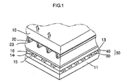
- An embodiment of the present invention shown in FIG. 1, includes a front substrate 10 and a rear substrate 11. Sustain electrodes 50 are formed on the rear substrate 11.
- the sustain electrodes 50 include a pair of electrodes 30, 40 (display electrodes and scanning electrodes) alternating with each other in the horizontal direction.
- a first dielectric film 15 covers the sustain electrodes 50.
- Address electrodes 14 are formed on the first dielectric film 15 and a second dielectric film 13 is positioned thereon.
- the address electrodes 14 crosses the sustain electrodes 50 while being perpendicular thereto, i.e., they intersect the sustain electrodes 50.
- a protective film 16, e.g., MgO, is formed on the second dielectric film 13.
- the sustain electrodes 50 and the address electrodes 14 are provided on inner portions of different substrates.
- Barrier ribs 20 are formed on the inner surface of the front substrate 10 facing the rear substrate 11.
- the barrier ribs 20 are formed in various shapes and by various methods.
- the front substrate 10 has a phosphor material 23, e.g., fluorescent layer, positioned for each cell on the inner surface thereof, i.e., on the surface having the barrier ribs 20 thereon, as well as on sidewalls of the barrier ribs 20.
- the phosphor material 23 may be provided by various conventional methods.
- the phosphor material 23 may also be on the rear substrate 11.
- a PDP plasma display device according to the present invention is more fully described below with reference to FIG. 2.
- a PDP plasma display device according to an embodiment of the present invention includes a first substrate, a second substrate, a plurality of pixels 130, a plurality of address electrodes A, a plurality of sustain electrodes X and Y, and a plurality of barrier ribs 110.
- the first substrate may be formed of a single layer or multiple layers, wherein at least one layer may be any opaque material.
- the first substrate may include a metal layer coated with a dielectric layer.
- the second substrate may be formed parallel to the first substrate, such that additional layers, e.g., electrodes, dielectric layers, protective layers, pixels and so forth, may be formed between the first and second substrates, as will be discussed in more detail below.
- Each pixel 130 of the PDP includes three discharge cells.
- each pixel 130 includes a first discharge cell 130a capable of emitting red (R) visible light, a second discharge cell 130b capable of emitting green (G) visible light, and a third discharge cell 130c capable of emitting blue (B) visible light.
- the discharge cells may have any convenient shape as determined by one of ordinary skill in the art, e.g., rectangular.
- each pixel 130 are arranged in a triangular shape in this embodiment.
- the three discharge cells of one pixel 130 are arranged in two parallel rows, such that two discharge cells of the pixel 130 are formed in one row and the other one discharge cell of the pixel 130 is formed in a parallel row.
- each adjacent pixel 130 in a pixel row has an alternating orientation.
- the adjacent pixel 130 in the same pixel row has one discharging cell in the upper row and two discharging cells in the lower row, i.e., forming a delta ( ⁇ ), such that the two adjacent pixels 130 form a uniform structure of two parallel rows. For example, as illustrated in FIG.
- rows may refer to a direction along an x-axis, as illustrated in FIG. 2. This orientation may be parallel to a horizontal side of a screen. However, other orientations are not excluded from the scope of the present invention. It should further be noted that terminology such as “first” and “second” with respect to rows is employed to distinguish the rows and indicate their sequence.
- the discharging cells may be disposed sequentially in any repetitive order along each row, such that a triangular shape of a pixel 130 having each of the first, second and third discharging cells 130a, 130b and 130c may be formed.
- the first, second and third discharging cells 130a, 130b and 130c are disposed sequentially in a first row
- the third, first and second discharging cells 130c, 130a and 130b are disposed sequentially in a second horizontal row, such that the third discharging cell 130c in the second row is shifted horizontally, more accurately shifted by half cycle, to be positioned symmetrically with respect to the first and second discharging cells 130a and 130b in the first row. Therefore, a central vertical line crossing the third discharging cell 130c aligns with a center of a vertical gap between the first and second discharge cells 130a and 130b.
- the above described pixel 130 structure is sequentially repeated in this embodiment.
- the delta-shaped pixels 130 and the nabla-shaped pixels 130 are positioned alternately in a linear array having two parallel rows of discharging cells.
- the plurality of address electrodes A of the PDP may be formed in a stripe-like structure in a plane parallel to a plane of the pixel 130 rows. Further, the plurality of address electrodes A may be formed in parallel to one another at a predetermined angel with respect to the linear array of pixel 130 rows, e.g., perpendicularly to the linear array of pixels 130.
- the plurality of address electrodes A are formed such that each address electrode A overlaps with one discharge cell in each row of discharge cells, e.g., address electrode A m+1 overlaps with the first discharge cell 130a in the first row.
- the structure of the discharge cells may be such that, for example, six address electrodes A m+1 ...A m+6 may overlap with four pixels 130 formed in the first two rows, as illustrated in FIG. 2. Accordingly, an average number of address electrodes A assigned to each pixel 130 may be 1.5, i.e., the average number of address electrodes A assigned to each pixel 130 may be reduced by two as compared with the conventional art.
- the barrier ribs 110 of the PDP may be formed on the first substrate or the second substrate by any method known in the art, e.g., lithography, photolithography, and so forth, in a direction parallel to a direction of the address electrodes A, as illustrated in FIG. 2.
- the barrier ribs 110 may be formed in a plane perpendicular to a plane of the first and the second substrates of the PDP and therebetween to define a plurality of discharge cells, such that phosphor layers 140 may be laminated in the discharge cells.
- the barrier ribs 110 may form a skewed grid structure, as illustrated in FIG.
- each address electrode A may pass between the vertically, i.e., along a y-axis, vertically formed portions of barrier ribs 110 without overlapping therewith.
- each address electrode A may be positioned between two vertically formed portions of barrier ribs 110.
- the sustain electrodes i.e., common electrodes X and scan electrodes Y, of the PDP according to an embodiment of the present invention may be formed of metal or of a transparent conductive layer, e.g., indium-tin-oxide (ITO), on the second substrate.
- ITO indium-tin-oxide
- the sustain electrodes X and Y may be formed in an alternating stripe-like structure and parallel to one another, i.e., alternately disposing a common electrode X and a scan electrode Y perpendicularly to a direction of the address electrodes A.
- the sustain electrodes X and Y may be formed in parallel to the rows of discharge cells and perpendicularly to the vertically formed portions of the barrier ribs 110, such that one sustain electrode may be positioned between two rows of discharge cells, as illustrated in FIG.1.
- sustain electrode Y n+1 may be positioned between the first and second discharge cell rows
- sustain electrode X n+2 may be positioned between the second and third discharge cell rows.
- negative voltage may be applied to any scan electrode Y, e.g., Y n+1
- positive voltage may be applied to any address electrode A, e.g., A m+1 , to trigger discharge in two vertical discharge cells positioned adjacent to the scan electrode Y, e.g., the first discharge cell 130a and the third discharge cell 130c.
- the scan electrodes Y may be divided into a first scan electrode group Y 2n+1 and a second scan electrode group Y 2n , such that different voltages may be applied to each group to provide ALIS driving.
- ALIS lightening of surface
- a dielectric layer and/or a protective layer maybe disposed on the sustain electrodes X and Y by any method known in the art, e.g., sputtering, deposition, and so forth.
- the PDP according to an embodiment of the present invention may have a layered structure, such that the first and second substrates may have layers of electrodes, barrier ribs, dielectric materials, and protective materials therebetween. Such structure and methods of manufacturing thereof are well-known in the art, and therefore, will not be described in detail herein.
- a PDP according to an embodiment of the present invention may further include at least one branch electrode 125 electrically connected to each address electrode A in order to increase an area of a display and/or address discharge and allowing greater accuracy.
- each branch electrode 125 may be formed to overlap with a respective discharge cell, such that the branch electrode 125 may extend from the respective address electrode A towards a center of the respective discharge cell.
- each two vertically adjacent branch electrodes 125 in communication with a respective address electrode A may be directed in opposite directions.
- the shape, number, and angle with respect to the main address electrode A of the branch electrodes 125 may vary.
- the PDP is similar to the PDP described with respect to FIG. 2, with the exception that a first, a second, and a third discharge cell 230a, 230b, and 230c, respectively, of each pixel 230 may have a hexagonal form. Accordingly, only details that may be distinguishable from the previous embodiment will be described hereinafter.
- Each sustain electrode X and Y has a predetermined width and be made of any suitable material as determined by one of ordinary skill in the art.
- each sustain electrode includes a bus electrode 313 and a transparent electrode 315, as illustrated in FIG. 3.
- the transparent electrode 315 is in contact with the bus electrode 313 and has a sufficient width to overlap with portions of two rows of discharge cells.
- the sustain electrode Y n+1 has a transparent electrode 315 overlapping with a lower portion of the first row of discharge cells and with an upper portion of the second row of discharge cells.
- the formation of the discharge cells and the address electrodes A is similar to the formation described previously with respect to FIG. 2. Accordingly, the average number of address electrodes A assigned to each pixel 230 is 1.5 as well.
- sixteen pixels are illustrated in FIGS. 2 and 3, i.e., four pixels in each row and column. Since a total number of address electrodes A illustrated in each one of FIGS. 2 and 3 is six, and a total number of scan electrodes Y illustrated in each one of FIGS. 2 and 3 is four, a ratio of the number of the address electrodes A to the number of the scan electrodes Y is 3:2. Further, a ratio of the number of the address electrodes A with respect to a number of the sustain electrodes X and Y is 3:4.
- the embodiments of the present invention were compared to conventional PDPs having different configurations of barrier ribs and electrodes.
- the comparison parameters included number of address electrodes, number of TCPs, number of scan electrodes and scan driving circuits, the required number of address buffer boards, the address power consumption, heat generation per address circuit, and the critical power (instantaneous power) applied to each address circuit.
- the power consumption, heat generation, and critical power for each address electrode were estimated at the most conservative case scenario.
- Stripe, hexagonal discharge, and hexagonal meander indicate the structure of the barrier ribs with respect to the shape of the discharge cells. Further, single and dual scans were performed. A single scan refers to address driving performed at one side of the discharge cells' center, while dual scan refers to address driving performed at both sides of the discharge cells' center. FHD refers to a "full high definition type.”
- the most conservative case means the case of applying on voltage and off voltage alternatively to the address electrodes.
- the interference between the address electrodes, the parasitic capacitance causes increased power consumption and heat generation.
- the value of the table is gained by theoretical calculation not by experiment. Theoretically, the current flow increase as the distance between the address electrodes decrease, the 'power consumption' is proportional to capacitance and the square of voltage difference between the electrodes nearly disposed.
- a PDP according to an embodiment of the present invention may have a reduced number of address electrodes as compared to a conventional PDP having the same horizontal resolution and number of driving circuit chips, whereby overall power consumption and heat release rate are reduced.
Abstract
Description
- The present invention relates to a plasma display panel. More particularly, the present invention relates to a plasma display panel having enhanced integration degree of pixels.
- In general, a plasma display panel (PDP) refers to a flat display device capable of displaying images using gas discharge phenomenon, thereby providing superior display characteristic, such as high brightness and contrast, lack of residual image, and wide viewing angles.
- A conventional PDP may include two substrates with a plurality of discharging electrodes therebetween, i.e., a plurality of sustain and address electrodes, a plurality of pixels having phosphorescent layers, and barrier ribs between the two substrates to separate the plurality of phosphorescent layers. When a predetermined amount of electricity is applied to the electrodes, a sustain discharge may be generated to trigger ultraviolet (UV) emission and, thereby, to excite the phosphorescent layers to emit light and form visible images.
- Such a conventional PDP may be driven either by a direct current (DC) voltage or an alternating current (AC) voltage. When a conventional PDP is driven by an AC voltage, the driving electrodes may be coated with a dielectric layer to improve the electrostatic capacity thereof. Further, due to a reduced current flow through the driving electrodes, the exposure of the electrodes to discharge is minimized, thereby providing improved lifespan thereto. When a conventional PDP is driven by an AC surface discharge, as opposed to face-type discharge, a plurality of parallel address electrodes may be positioned vertically between the two substrates, and a plurality of common and scan electrodes, e.g., pairs of sustain and display electrodes, may be positioned parallel to one another in alternating horizontal stripe-pattern between the two substrates.
- A matrix of pixels may be formed between the plurality of address electrodes and pairs of sustain and display electrodes, while each pixel may include discharge cells emitting separate visible light beams. The discharge cells of each pixel may be sequentially arranged in stripe-shaped or circle-shaped structures, such that each pixel may overlap with three address electrodes. The arrangement and structure of pixels may affect high definition and high brightness in a PDP. Accordingly, attempts have been made to increase the pixel density.
- However, an increase of pixel density may increase the number of required address electrodes. An increased number of address electrodes may reduce the distance therebetween and, therefore, increase the capacitance, the power consumption, and the heat release rate of the PDP, thereby reducing its signal transmittance. Additionally, an increased number of address electrodes may increase the cost and complexity of the manufacturing process due to additional required elements, e.g., tape carrier packages (TCP), and difficulty in designing an appropriate driving board.
- Accordingly, there exists a need to improve the structure of a PDP in order to provide for an improved pixel density, while maintaining a reduced number of address electrodes.
- The present invention is therefore directed to a plasma display panel which substantially overcomes one or more of the disadvantages of the related art.
- It is therefore a feature of an embodiment of the present invention to provide a plasma display panel capable of providing increased pixel density, while maintaining a reduced number of address electrodes.
- It is another feature of an embodiment of the present invention to provide a plasma display panel capable of reducing power consumption and manufacturing costs.
- According to a first aspect of the invention, there is provided a plasma display panel as set out in
Claim 1. Preferred features of this aspect are set on inClaims 2 to 17. - According to a second aspect of the invention, there is provided a a plasma display panel as set out in Claim 18. Preferred features of this aspect are set on in
Claims 19 and 20. - The above and other features and advantages of the present invention will become more apparent to those of ordinary skill in the art by describing in detail exemplary embodiments thereof with reference to the attached drawings, in which:
- FIG. 1 illustrate a perspective sectional view of a plasma display panel according to an embodiment of the present invention;
- FIG. 2 illustrates a schematic plan view of a plasma display panel according to another embodiment of the present invention; and
- FIG. 3 illustrates a schematic plan view of a plasma display panel according to the other embodiment of the present invention.
- The present invention will now be described more fully hereinafter with reference to the accompanying drawings, in which exemplary embodiments of the invention are illustrated. The invention may, however, be embodied in different forms and should not be construed as limited to the embodiments set forth herein. Rather, these embodiments are provided so that this disclosure will be thorough and complete, and will fully convey the scope of the invention to those skilled in the art.
- It will further be understood that when an element is referred to as being "on" another element or substrate, it can be directly on the other element or substrate, or intervening elements may also be present. Further, it will be understood that when an element is referred to as being "under" another element, it can be directly under, or one or more intervening elements may also be present. In addition, it will also be understood that when an element is referred to as being "between" two elements, it can be the only element between the two elements, or one or more intervening elements may also be present. Like reference numerals refer to like elements throughout.
- A PDP according to an embodiment of the present invention includes a first substrate, a second substrate, a plurality of pixels disposed between the first and second substrates, and a plurality of driving electrodes formed on the first substrate, the second substrate, or both.
- An embodiment of the present invention, shown in FIG. 1, includes a
front substrate 10 and arear substrate 11. Sustain electrodes 50 are formed on therear substrate 11. The sustain electrodes 50 include a pair ofelectrodes 30, 40 (display electrodes and scanning electrodes) alternating with each other in the horizontal direction. A firstdielectric film 15 covers the sustain electrodes 50. Address electrodes 14 are formed on the firstdielectric film 15 and a seconddielectric film 13 is positioned thereon. The address electrodes 14 crosses the sustain electrodes 50 while being perpendicular thereto, i.e., they intersect the sustain electrodes 50. A protective film 16, e.g., MgO, is formed on the seconddielectric film 13. The sustain electrodes 50 and the address electrodes 14 are provided on inner portions of different substrates. -
Barrier ribs 20 are formed on the inner surface of thefront substrate 10 facing therear substrate 11. Thebarrier ribs 20 are formed in various shapes and by various methods. Thefront substrate 10 has a phosphor material 23, e.g., fluorescent layer, positioned for each cell on the inner surface thereof, i.e., on the surface having the barrier ribs 20 thereon, as well as on sidewalls of thebarrier ribs 20. The phosphor material 23 may be provided by various conventional methods. The phosphor material 23 may also be on therear substrate 11. - An embodiment of a plasma display device (PDP) according to the present invention is more fully described below with reference to FIG. 2. As illustrated in FIG. 2, a PDP according to an embodiment of the present invention includes a first substrate, a second substrate, a plurality of pixels 130, a plurality of address electrodes A, a plurality of sustain electrodes X and Y, and a plurality of
barrier ribs 110. - The first substrate may be formed of a single layer or multiple layers, wherein at least one layer may be any opaque material. For example, the first substrate may include a metal layer coated with a dielectric layer. The second substrate may be formed parallel to the first substrate, such that additional layers, e.g., electrodes, dielectric layers, protective layers, pixels and so forth, may be formed between the first and second substrates, as will be discussed in more detail below.
- Each pixel 130 of the PDP according to an embodiment of the present invention includes three discharge cells. In particular, as further illustrated in FIG. 2, each pixel 130 includes a first discharge cell 130a capable of emitting red (R) visible light, a
second discharge cell 130b capable of emitting green (G) visible light, and athird discharge cell 130c capable of emitting blue (B) visible light. The discharge cells may have any convenient shape as determined by one of ordinary skill in the art, e.g., rectangular. - The discharge cells of each pixel 130 are arranged in a triangular shape in this embodiment. In particular, the three discharge cells of one pixel 130 are arranged in two parallel rows, such that two discharge cells of the pixel 130 are formed in one row and the other one discharge cell of the pixel 130 is formed in a parallel row. Further, each adjacent pixel 130 in a pixel row has an alternating orientation. In other words, if one pixel 130 has two discharging cells in an upper row and one discharging cell in a lower row, i.e., forming a nabla (∇), the adjacent pixel 130 in the same pixel row has one discharging cell in the upper row and two discharging cells in the lower row, i.e., forming a delta (Δ), such that the two adjacent pixels 130 form a uniform structure of two parallel rows. For example, as illustrated in FIG. 2, if one pixel 130 has the first and second discharging
cells 130a and 130b in the upper row and the third dischargingcell 130c in the lower row, the adjacent pixel 130 has the first and second dischargingcells 130a and 130b in the lower row and the third dischargingcell 130c in the upper row. - In this respect, it should be noted that "rows" may refer to a direction along an x-axis, as illustrated in FIG. 2. This orientation may be parallel to a horizontal side of a screen. However, other orientations are not excluded from the scope of the present invention. It should further be noted that terminology such as "first" and "second" with respect to rows is employed to distinguish the rows and indicate their sequence.
- The discharging cells may be disposed sequentially in any repetitive order along each row, such that a triangular shape of a pixel 130 having each of the first, second and third discharging
cells cells cells cell 130c in the second row is shifted horizontally, more accurately shifted by half cycle, to be positioned symmetrically with respect to the first and second dischargingcells 130a and 130b in the first row. Therefore, a central vertical line crossing the third dischargingcell 130c aligns with a center of a vertical gap between the first andsecond discharge cells 130a and 130b. - The above described pixel 130 structure is sequentially repeated in this embodiment. In other words, the delta-shaped pixels 130 and the nabla-shaped pixels 130 are positioned alternately in a linear array having two parallel rows of discharging cells.
- The plurality of address electrodes A of the PDP according to an embodiment of the present invention may be formed in a stripe-like structure in a plane parallel to a plane of the pixel 130 rows. Further, the plurality of address electrodes A may be formed in parallel to one another at a predetermined angel with respect to the linear array of pixel 130 rows, e.g., perpendicularly to the linear array of pixels 130.
- The plurality of address electrodes A are formed such that each address electrode A overlaps with one discharge cell in each row of discharge cells, e.g., address electrode Am+1 overlaps with the first discharge cell 130a in the first row. However, the structure of the discharge cells may be such that, for example, six address electrodes Am+1...Am+6 may overlap with four pixels 130 formed in the first two rows, as illustrated in FIG. 2. Accordingly, an average number of address electrodes A assigned to each pixel 130 may be 1.5, i.e., the average number of address electrodes A assigned to each pixel 130 may be reduced by two as compared with the conventional art.
- The
barrier ribs 110 of the PDP according to an embodiment of the present invention may be formed on the first substrate or the second substrate by any method known in the art, e.g., lithography, photolithography, and so forth, in a direction parallel to a direction of the address electrodes A, as illustrated in FIG. 2. In particular thebarrier ribs 110 may be formed in a plane perpendicular to a plane of the first and the second substrates of the PDP and therebetween to define a plurality of discharge cells, such that phosphor layers 140 may be laminated in the discharge cells. More specifically, thebarrier ribs 110 may form a skewed grid structure, as illustrated in FIG. 2, such that the address electrodes A may pass between the vertically, i.e., along a y-axis, vertically formed portions ofbarrier ribs 110 without overlapping therewith. In other words, each address electrode A may be positioned between two vertically formed portions ofbarrier ribs 110. - The sustain electrodes, i.e., common electrodes X and scan electrodes Y, of the PDP according to an embodiment of the present invention may be formed of metal or of a transparent conductive layer, e.g., indium-tin-oxide (ITO), on the second substrate. In particular, the sustain electrodes X and Y may be formed in an alternating stripe-like structure and parallel to one another, i.e., alternately disposing a common electrode X and a scan electrode Y perpendicularly to a direction of the address electrodes A. In particular, the sustain electrodes X and Y may be formed in parallel to the rows of discharge cells and perpendicularly to the vertically formed portions of the
barrier ribs 110, such that one sustain electrode may be positioned between two rows of discharge cells, as illustrated in FIG.1. For example, sustain electrode Yn+1 may be positioned between the first and second discharge cell rows, while the sustain electrode Xn+2 may be positioned between the second and third discharge cell rows. For example, negative voltage may be applied to any scan electrode Y, e.g., Yn+1, and positive voltage may be applied to any address electrode A, e.g., Am+1, to trigger discharge in two vertical discharge cells positioned adjacent to the scan electrode Y, e.g., the first discharge cell 130a and thethird discharge cell 130c. - Without intending to be bound by theory, it is believed that employing two types of sustain electrodes X and Y on the
barrier ribs 110 may provide a longer gap and a face discharge type PDP, thereby increasing the distance between discharge electrodes and overall discharge efficiency. - It should be noted; however, that when a discharge is triggered simultaneously in two vertically adjacent discharge cells, the two discharge cells may not be driven independently, thereby reducing vertical resolution of the PDP. Accordingly, an alternative lightening of surface (ALIS) method may be applied. For example, the scan electrodes Y may be divided into a first scan electrode group Y2n+1 and a second scan electrode group Y2n, such that different voltages may be applied to each group to provide ALIS driving. Other known methods of ALIS may be employed in the present invention as determined by one of ordinary skill in the art. However, since the ALIS method is well known, detailed description thereof will be omitted herein.
- A dielectric layer and/or a protective layer maybe disposed on the sustain electrodes X and Y by any method known in the art, e.g., sputtering, deposition, and so forth. Accordingly, the PDP according to an embodiment of the present invention may have a layered structure, such that the first and second substrates may have layers of electrodes, barrier ribs, dielectric materials, and protective materials therebetween. Such structure and methods of manufacturing thereof are well-known in the art, and therefore, will not be described in detail herein.
- A PDP according to an embodiment of the present invention may further include at least one
branch electrode 125 electrically connected to each address electrode A in order to increase an area of a display and/or address discharge and allowing greater accuracy. For example, eachbranch electrode 125 may be formed to overlap with a respective discharge cell, such that thebranch electrode 125 may extend from the respective address electrode A towards a center of the respective discharge cell. Accordingly, as illustrated in FIG. 2, each two verticallyadjacent branch electrodes 125 in communication with a respective address electrode A may be directed in opposite directions. In this respect, it should be noted that the shape, number, and angle with respect to the main address electrode A of thebranch electrodes 125 may vary. - In another embodiment of the present invention as illustrated in FIG. 3, the PDP is similar to the PDP described with respect to FIG. 2, with the exception that a first, a second, and a
third discharge cell pixel 230 may have a hexagonal form. Accordingly, only details that may be distinguishable from the previous embodiment will be described hereinafter. - Each sustain electrode X and Y has a predetermined width and be made of any suitable material as determined by one of ordinary skill in the art. In particular, each sustain electrode includes a
bus electrode 313 and atransparent electrode 315, as illustrated in FIG. 3. Thetransparent electrode 315 is in contact with thebus electrode 313 and has a sufficient width to overlap with portions of two rows of discharge cells. As illustrated in FIG. 3, the sustain electrode Yn+1 has atransparent electrode 315 overlapping with a lower portion of the first row of discharge cells and with an upper portion of the second row of discharge cells. - The formation of the discharge cells and the address electrodes A is similar to the formation described previously with respect to FIG. 2. Accordingly, the average number of address electrodes A assigned to each
pixel 230 is 1.5 as well. - Additionally, in both embodiments described above, sixteen pixels are illustrated in FIGS. 2 and 3, i.e., four pixels in each row and column. Since a total number of address electrodes A illustrated in each one of FIGS. 2 and 3 is six, and a total number of scan electrodes Y illustrated in each one of FIGS. 2 and 3 is four, a ratio of the number of the address electrodes A to the number of the scan electrodes Y is 3:2. Further, a ratio of the number of the address electrodes A with respect to a number of the sustain electrodes X and Y is 3:4.
- EXAMPLES:
- The embodiments of the present invention were compared to conventional PDPs having different configurations of barrier ribs and electrodes. The comparison parameters included number of address electrodes, number of TCPs, number of scan electrodes and scan driving circuits, the required number of address buffer boards, the address power consumption, heat generation per address circuit, and the critical power (instantaneous power) applied to each address circuit. The power consumption, heat generation, and critical power for each address electrode were estimated at the most conservative case scenario.
- Stripe, hexagonal discharge, and hexagonal meander indicate the structure of the barrier ribs with respect to the shape of the discharge cells. Further, single and dual scans were performed. A single scan refers to address driving performed at one side of the discharge cells' center, while dual scan refers to address driving performed at both sides of the discharge cells' center. FHD refers to a "full high definition type."
- Results of the comparison are summarized in Table 1 below.
- In relation with the table, We assume that, the power used for driving the address electrode is fully consumed as the switching is made, the voltage level for driving the address electrode is fixed for all cases.
- The most conservative case means the case of applying on voltage and off voltage alternatively to the address electrodes. In the case, the interference between the address electrodes, the parasitic capacitance causes increased power consumption and heat generation.
- The value of the table is gained by theoretical calculation not by experiment. Theoretically, the current flow increase as the distance between the address electrodes decrease, the 'power consumption' is proportional to capacitance and the square of voltage difference between the electrodes nearly disposed. In the table, the number of address electrode in hexagonal meander type is 4089 and that of address electrode in new delta type, the present invention type is 2880. If the size of the panel is same, the power consumption is decreased by 2880/4089=0.69.
Table 1 Type/item Number of address electrodes Number of TCP Number of required buffer board Power consumption for address electrodes Heat generation per address electrode Critical power per address buffer board Number of scan electrodes Number of scan driving chips Embodiment of the Present invention FHD, Dual 2880 30 2 0.69 0.49 0.35 1080 17 Stripe FHD, Dual 5760 60 2 1.39 0.49 0.7 1080 17 Hexagonal discharge FHD, Dual 5760 60 2 1.39 0.49 0.7 1080 17 Hexagonal meander FHD, Single 5760 30 1 2.78 1.98 1.41 1080 17 Hexagonal meander 1366*768, Single 4098 21 1 1 1 1 768 12 Hexagonal meander 1280*720, Single 3840 20 1 0.82 0.88 0.94 720 12 - As illustrated in Table 1, embodiments of the present invention have a reduced number of address electrodes as compared to conventional art, while exhibiting reduced power consumption per address electrode, reduced heat generation per address electrode, and reduced critical power per address electrode. Accordingly, a PDP according to an embodiment of the present invention may have a reduced number of address electrodes as compared to a conventional PDP having the same horizontal resolution and number of driving circuit chips, whereby overall power consumption and heat release rate are reduced.
- Embodiments of the present invention have been disclosed herein, and although specific terms are employed, they are used and are to be interpreted in a generic and descriptive sense only and not for purpose of limitation. Accordingly, it will be understood by those of ordinary skill in the art that various changes in form and details may be made without departing from the scope of the present invention as set forth in the following claims.
Claims (20)
- A plasma display panel comprising:two substrates;a plurality of barrier ribs arranged between the two substrates, the plurality of barrier ribs defining a plurality of discharge cells;a plurality of pixel rows arranged between the two substrates, each pixel row having a plurality of pixels, wherein each pixel includes three discharge cells arranged in a triangular shape; anda plurality of address electrodes arranged between the two substrates, wherein an average of 1.5 address electrodes are assigned to each pixel in a pixel row.
- A plasma display panel according to claim 1,
wherein the three discharge cells of each pixel are arranged in either a delta shape or a nabla shape to form a triangle,
wherein said pixel row includes pixels in which the discharge cells are alternately arranged in the delta shape and in the nabla shape, and
wherein two of the address electrodes pass through each of the pixels. - A plasma display panel according to claim 1 or 2,
wherein each pixel row include a first row and a second row of discharge cells,
wherein the second row is shifted horizontally with respect to the first row. - A plasma display panel according to claim 3,
wherein the discharge cells of each pixel are arranged to emit one of three colors of light, wherein the second row is arranged to be shifted horizontally with respect to the first row by 1/2 a cycle. - A plasma display panel according to any one of claims 1 to 4,
wherein the address electrodes are perpendicular to each pixel row. - A plasma display panel according to any one of claims 1 to 5,
wherein the address electrodes and the vertical portions of the barrier ribs are positioned alternatively in each pixel row. - A plasma display panel according to any one of claims 1 to 6,further comprising at least one branch electrode electrically connected to each address electrode, the at least one branch electrode assigned to one discharge cell.
- A plasma display panel according to claim 7,
wherein the at least one branch electrode of each address electrode is arranged to extend from the address electrode toward a center of the overlapping discharge cell. - A plasma display panel according to any one of claims 1 to 8,further comprising a plurality of sustain electrodes positioned perpendicularly to the address electrodes.
- A plasma display panel according to claim 9,
wherein the sustain electrodes are positioned to have predetermined intervals therebetween. - A plasma display panel according to claim 10, wherein the sustain electrodes are arranged to overlap with horizontal portions of the plurality of the barrier ribs.
- A plasma display panel according to claim 10 or 11,
wherein the plurality of sustain electrodes includes alternating scan and common electrodes. - A plasma display panel according to claim 12,
wherein each pixel row is assigned to one common electrode and one scan electrode. - A plasma display panel according to claim 12 or 13,
wherein the common electrodes include a first group of common electrodes and a second group of common electrodes, the first and second groups of common electrodes having different voltages. - A plasma display panel according to any one of claims 1 to 14,
wherein the barrier ribs are arranged in a skewed-grid shape. - A plasma display panel according to any one of claims 1 to 15,
wherein the discharge cells have a hexagonal form or a rectangular form. - A plasma display panel according to any one of claims 1 to 16,further including a plurality of phosphorescent layers.
- A plasma display panel comprising:two substrates;a plurality of barrier ribs arranged between the two substrates, the plurality of barrier ribs defining a plurality of discharge cells;a plurality of pixel rows arranged between the two substrates, each pixel row having a plurality of pixels, wherein each pixel includes three discharge cells arranged in a triangular shape; anda plurality of address electrodes arranged between the two substrates,a plurality of sustain electrodes positioned perpendicularly to the address electrodes, wherein a ratio of a number of the address electrodes to a number of the sustain electrodes is about 3:4.
- A plasma display panel according to claim 18,
wherein the discharge cells of each pixel are arranged in either a delta shape or a nabla shape to form a triangle,
wherein the said pixel row include pixels in which the discharge cells are alternately arranged in the delta shape and in the nabla shape, and
wherein two of the address electrodes pass through each of the pixels. - A plasma display panel according to claim 18 or 19,
wherein each pixel row include a first row and a second row of discharge cells,
wherein discharge cells of each pixel are arranged to emit one of three colors of light,
wherein the second row is shifted horizontally with respect to the first row by 1/2 cycle.
Applications Claiming Priority (1)
| Application Number | Priority Date | Filing Date | Title |
|---|---|---|---|
| KR1020050111911A KR100788576B1 (en) | 2005-11-22 | 2005-11-22 | Plasma display panel for increasing the degree of integration of pixel |
Publications (2)
| Publication Number | Publication Date |
|---|---|
| EP1788609A2 true EP1788609A2 (en) | 2007-05-23 |
| EP1788609A3 EP1788609A3 (en) | 2008-10-29 |
Family
ID=37998362
Family Applications (1)
| Application Number | Title | Priority Date | Filing Date |
|---|---|---|---|
| EP06255959A Withdrawn EP1788609A3 (en) | 2005-11-22 | 2006-11-22 | Plasma display panel with increased integration degree of pixels |
Country Status (5)
| Country | Link |
|---|---|
| US (1) | US20070114938A1 (en) |
| EP (1) | EP1788609A3 (en) |
| JP (1) | JP2007141818A (en) |
| KR (1) | KR100788576B1 (en) |
| CN (1) | CN1971828A (en) |
Cited By (1)
| Publication number | Priority date | Publication date | Assignee | Title |
|---|---|---|---|---|
| EP1870921A2 (en) * | 2006-06-21 | 2007-12-26 | Samsung SDI Co., Ltd. | Plasma display panel |
Families Citing this family (2)
| Publication number | Priority date | Publication date | Assignee | Title |
|---|---|---|---|---|
| KR100659834B1 (en) * | 2005-11-22 | 2006-12-19 | 삼성에스디아이 주식회사 | Plasma display panel suitable for mono color display |
| KR20100042795A (en) * | 2008-10-17 | 2010-04-27 | 삼성에스디아이 주식회사 | Plasma display panel and method of manufacturing the same |
Citations (5)
| Publication number | Priority date | Publication date | Assignee | Title |
|---|---|---|---|---|
| WO2003079392A2 (en) * | 2002-03-19 | 2003-09-25 | Koninklijke Philips Electronics N.V. | Plasma display panel electrode and phosphor structure |
| US20040178972A1 (en) * | 2003-02-20 | 2004-09-16 | Ji-Bin Du | Driving method for a plasma display panel |
| US20050057172A1 (en) * | 2003-08-20 | 2005-03-17 | Yao-Ching Su | [alternating current plasma display panel] |
| WO2005059943A1 (en) * | 2003-12-17 | 2005-06-30 | Hitachi Plasma Patent Licensing Co., Ltd. | Plasma display panel |
| EP1786013A2 (en) * | 2005-11-15 | 2007-05-16 | Samsung SDI Co., Ltd. | Plasma display panel |
Family Cites Families (9)
| Publication number | Priority date | Publication date | Assignee | Title |
|---|---|---|---|---|
| KR100408213B1 (en) * | 2000-06-26 | 2003-12-01 | 황기웅 | an AC plasma display panel having delta color pixels of closed shape subpixels |
| KR20020056443A (en) * | 2000-12-29 | 2002-07-10 | 엘지전자 주식회사 | Plasma display panel |
| JP2002251165A (en) * | 2001-02-22 | 2002-09-06 | Mitsubishi Electric Corp | Plasma display panel, driving device for plasma display panel, plasma display device and driving method for plasma display panel |
| KR20030037293A (en) * | 2001-11-01 | 2003-05-14 | 엘지전자 주식회사 | Plasma display panel |
| US6806645B2 (en) * | 2001-10-24 | 2004-10-19 | Lg Electronics Inc. | Plasma display panel |
| KR100482325B1 (en) * | 2002-03-14 | 2005-04-13 | 엘지전자 주식회사 | Plasma display panel |
| TWI220052B (en) * | 2002-11-25 | 2004-08-01 | Au Optronics Corp | Plasma display panel having shared data electrodes |
| KR100589341B1 (en) * | 2004-02-25 | 2006-06-14 | 삼성에스디아이 주식회사 | Plasma display panel |
| KR100578878B1 (en) * | 2004-04-29 | 2006-05-11 | 삼성에스디아이 주식회사 | Plasma display panel |
-
2005
- 2005-11-22 KR KR1020050111911A patent/KR100788576B1/en not_active IP Right Cessation
-
2006
- 2006-10-10 JP JP2006276873A patent/JP2007141818A/en active Pending
- 2006-11-22 US US11/603,193 patent/US20070114938A1/en not_active Abandoned
- 2006-11-22 EP EP06255959A patent/EP1788609A3/en not_active Withdrawn
- 2006-11-22 CN CNA2006101723925A patent/CN1971828A/en active Pending
Patent Citations (5)
| Publication number | Priority date | Publication date | Assignee | Title |
|---|---|---|---|---|
| WO2003079392A2 (en) * | 2002-03-19 | 2003-09-25 | Koninklijke Philips Electronics N.V. | Plasma display panel electrode and phosphor structure |
| US20040178972A1 (en) * | 2003-02-20 | 2004-09-16 | Ji-Bin Du | Driving method for a plasma display panel |
| US20050057172A1 (en) * | 2003-08-20 | 2005-03-17 | Yao-Ching Su | [alternating current plasma display panel] |
| WO2005059943A1 (en) * | 2003-12-17 | 2005-06-30 | Hitachi Plasma Patent Licensing Co., Ltd. | Plasma display panel |
| EP1786013A2 (en) * | 2005-11-15 | 2007-05-16 | Samsung SDI Co., Ltd. | Plasma display panel |
Cited By (2)
| Publication number | Priority date | Publication date | Assignee | Title |
|---|---|---|---|---|
| EP1870921A2 (en) * | 2006-06-21 | 2007-12-26 | Samsung SDI Co., Ltd. | Plasma display panel |
| EP1870921A3 (en) * | 2006-06-21 | 2010-01-20 | Samsung SDI Co., Ltd. | Plasma display panel |
Also Published As
| Publication number | Publication date |
|---|---|
| CN1971828A (en) | 2007-05-30 |
| KR100788576B1 (en) | 2007-12-26 |
| KR20070053992A (en) | 2007-05-28 |
| EP1788609A3 (en) | 2008-10-29 |
| JP2007141818A (en) | 2007-06-07 |
| US20070114938A1 (en) | 2007-05-24 |
Similar Documents
| Publication | Publication Date | Title |
|---|---|---|
| JP2003068209A (en) | Plasma display panel | |
| JP2003331741A (en) | Plasma display panel | |
| US20050264232A1 (en) | Plasma display panel | |
| US7098594B2 (en) | Plasma display panel having delta pixel arrangement | |
| EP1788609A2 (en) | Plasma display panel with increased integration degree of pixels | |
| CN1265518A (en) | Panel display | |
| KR100612244B1 (en) | Plasma display panel | |
| EP1786013A2 (en) | Plasma display panel | |
| US7728522B2 (en) | Plasma display panel | |
| US7642718B2 (en) | Plasma display panel with wider and narrower display regions | |
| US7667402B2 (en) | Plasma display panel and method of fabricating the same | |
| EP1755140A1 (en) | Plasma display panel | |
| US20080094317A1 (en) | Plasma display panel | |
| US20070018913A1 (en) | Plasma display panel, plasma display device and driving method therefor | |
| US20050122045A1 (en) | Plasma display panel | |
| KR100658726B1 (en) | Plasma display panel | |
| US7508136B2 (en) | Plasma display panel | |
| KR100447127B1 (en) | Plasma display panel | |
| US20050253514A1 (en) | Plasma display panel | |
| KR100322083B1 (en) | Plasma display panel | |
| US7667404B2 (en) | Plasma display apparatus | |
| KR100684851B1 (en) | Plasma display panel | |
| KR100590079B1 (en) | Plasma display panel | |
| US20070114934A1 (en) | Plasma display panel (PDP) suitable for monochromatic display | |
| JP2008004528A (en) | Plasma display panel |
Legal Events
| Date | Code | Title | Description |
|---|---|---|---|
| PUAI | Public reference made under article 153(3) epc to a published international application that has entered the european phase |
Free format text: ORIGINAL CODE: 0009012 |
|
| 17P | Request for examination filed |
Effective date: 20061128 |
|
| AK | Designated contracting states |
Kind code of ref document: A2 Designated state(s): AT BE BG CH CY CZ DE DK EE ES FI FR GB GR HU IE IS IT LI LT LU LV MC NL PL PT RO SE SI SK TR |
|
| AX | Request for extension of the european patent |
Extension state: AL BA HR MK YU |
|
| PUAL | Search report despatched |
Free format text: ORIGINAL CODE: 0009013 |
|
| AK | Designated contracting states |
Kind code of ref document: A3 Designated state(s): AT BE BG CH CY CZ DE DK EE ES FI FR GB GR HU IE IS IT LI LT LU LV MC NL PL PT RO SE SI SK TR |
|
| AX | Request for extension of the european patent |
Extension state: AL BA HR MK RS |
|
| RIC1 | Information provided on ipc code assigned before grant |
Ipc: H01J 17/04 20060101ALI20080925BHEP Ipc: H01J 17/49 20060101AFI20070122BHEP |
|
| 17Q | First examination report despatched |
Effective date: 20090602 |
|
| AKX | Designation fees paid |
Designated state(s): DE FR GB |
|
| STAA | Information on the status of an ep patent application or granted ep patent |
Free format text: STATUS: THE APPLICATION HAS BEEN WITHDRAWN |
|
| 18W | Application withdrawn |
Effective date: 20091221 |