EP1787786A2 - Extrusion/dispensing systems and methods - Google Patents
Extrusion/dispensing systems and methods Download PDFInfo
- Publication number
- EP1787786A2 EP1787786A2 EP06123903A EP06123903A EP1787786A2 EP 1787786 A2 EP1787786 A2 EP 1787786A2 EP 06123903 A EP06123903 A EP 06123903A EP 06123903 A EP06123903 A EP 06123903A EP 1787786 A2 EP1787786 A2 EP 1787786A2
- Authority
- EP
- European Patent Office
- Prior art keywords
- materials
- channels
- applicator
- housing
- substrate
- Prior art date
- Legal status (The legal status is an assumption and is not a legal conclusion. Google has not performed a legal analysis and makes no representation as to the accuracy of the status listed.)
- Granted
Links
Images


Classifications
-
- B—PERFORMING OPERATIONS; TRANSPORTING
- B05—SPRAYING OR ATOMISING IN GENERAL; APPLYING FLUENT MATERIALS TO SURFACES, IN GENERAL
- B05C—APPARATUS FOR APPLYING FLUENT MATERIALS TO SURFACES, IN GENERAL
- B05C11/00—Component parts, details or accessories not specifically provided for in groups B05C1/00 - B05C9/00
- B05C11/10—Storage, supply or control of liquid or other fluent material; Recovery of excess liquid or other fluent material
- B05C11/105—Storage, supply or control of liquid or other fluent material; Recovery of excess liquid or other fluent material by capillary action, e.g. using wicks
-
- B—PERFORMING OPERATIONS; TRANSPORTING
- B05—SPRAYING OR ATOMISING IN GENERAL; APPLYING FLUENT MATERIALS TO SURFACES, IN GENERAL
- B05B—SPRAYING APPARATUS; ATOMISING APPARATUS; NOZZLES
- B05B9/00—Spraying apparatus for discharge of liquids or other fluent material, without essentially mixing with gas or vapour
- B05B9/03—Spraying apparatus for discharge of liquids or other fluent material, without essentially mixing with gas or vapour characterised by means for supplying liquid or other fluent material
- B05B9/04—Spraying apparatus for discharge of liquids or other fluent material, without essentially mixing with gas or vapour characterised by means for supplying liquid or other fluent material with pressurised or compressible container; with pump
- B05B9/06—Spraying apparatus for discharge of liquids or other fluent material, without essentially mixing with gas or vapour characterised by means for supplying liquid or other fluent material with pressurised or compressible container; with pump the delivery being related to the movement of a vehicle, e.g. the pump being driven by a vehicle wheel
-
- B—PERFORMING OPERATIONS; TRANSPORTING
- B05—SPRAYING OR ATOMISING IN GENERAL; APPLYING FLUENT MATERIALS TO SURFACES, IN GENERAL
- B05C—APPARATUS FOR APPLYING FLUENT MATERIALS TO SURFACES, IN GENERAL
- B05C19/00—Apparatus specially adapted for applying particulate materials to surfaces
- B05C19/04—Apparatus specially adapted for applying particulate materials to surfaces the particulate material being projected, poured or allowed to flow onto the surface of the work
-
- B—PERFORMING OPERATIONS; TRANSPORTING
- B05—SPRAYING OR ATOMISING IN GENERAL; APPLYING FLUENT MATERIALS TO SURFACES, IN GENERAL
- B05C—APPARATUS FOR APPLYING FLUENT MATERIALS TO SURFACES, IN GENERAL
- B05C5/00—Apparatus in which liquid or other fluent material is projected, poured or allowed to flow on to the surface of the work
- B05C5/02—Apparatus in which liquid or other fluent material is projected, poured or allowed to flow on to the surface of the work the liquid or other fluent material being discharged through an outlet orifice by pressure, e.g. from an outlet device in contact or almost in contact, with the work
- B05C5/0254—Coating heads with slot-shaped outlet
-
- B—PERFORMING OPERATIONS; TRANSPORTING
- B05—SPRAYING OR ATOMISING IN GENERAL; APPLYING FLUENT MATERIALS TO SURFACES, IN GENERAL
- B05C—APPARATUS FOR APPLYING FLUENT MATERIALS TO SURFACES, IN GENERAL
- B05C9/00—Apparatus or plant for applying liquid or other fluent material to surfaces by means not covered by any preceding group, or in which the means of applying the liquid or other fluent material is not important
-
- B—PERFORMING OPERATIONS; TRANSPORTING
- B29—WORKING OF PLASTICS; WORKING OF SUBSTANCES IN A PLASTIC STATE IN GENERAL
- B29C—SHAPING OR JOINING OF PLASTICS; SHAPING OF MATERIAL IN A PLASTIC STATE, NOT OTHERWISE PROVIDED FOR; AFTER-TREATMENT OF THE SHAPED PRODUCTS, e.g. REPAIRING
- B29C48/00—Extrusion moulding, i.e. expressing the moulding material through a die or nozzle which imparts the desired form; Apparatus therefor
- B29C48/03—Extrusion moulding, i.e. expressing the moulding material through a die or nozzle which imparts the desired form; Apparatus therefor characterised by the shape of the extruded material at extrusion
- B29C48/05—Filamentary, e.g. strands
-
- B—PERFORMING OPERATIONS; TRANSPORTING
- B29—WORKING OF PLASTICS; WORKING OF SUBSTANCES IN A PLASTIC STATE IN GENERAL
- B29C—SHAPING OR JOINING OF PLASTICS; SHAPING OF MATERIAL IN A PLASTIC STATE, NOT OTHERWISE PROVIDED FOR; AFTER-TREATMENT OF THE SHAPED PRODUCTS, e.g. REPAIRING
- B29C48/00—Extrusion moulding, i.e. expressing the moulding material through a die or nozzle which imparts the desired form; Apparatus therefor
- B29C48/03—Extrusion moulding, i.e. expressing the moulding material through a die or nozzle which imparts the desired form; Apparatus therefor characterised by the shape of the extruded material at extrusion
- B29C48/12—Articles with an irregular circumference when viewed in cross-section, e.g. window profiles
-
- B—PERFORMING OPERATIONS; TRANSPORTING
- B29—WORKING OF PLASTICS; WORKING OF SUBSTANCES IN A PLASTIC STATE IN GENERAL
- B29C—SHAPING OR JOINING OF PLASTICS; SHAPING OF MATERIAL IN A PLASTIC STATE, NOT OTHERWISE PROVIDED FOR; AFTER-TREATMENT OF THE SHAPED PRODUCTS, e.g. REPAIRING
- B29C48/00—Extrusion moulding, i.e. expressing the moulding material through a die or nozzle which imparts the desired form; Apparatus therefor
- B29C48/16—Articles comprising two or more components, e.g. co-extruded layers
- B29C48/18—Articles comprising two or more components, e.g. co-extruded layers the components being layers
- B29C48/19—Articles comprising two or more components, e.g. co-extruded layers the components being layers the layers being joined at their edges
-
- B—PERFORMING OPERATIONS; TRANSPORTING
- B29—WORKING OF PLASTICS; WORKING OF SUBSTANCES IN A PLASTIC STATE IN GENERAL
- B29C—SHAPING OR JOINING OF PLASTICS; SHAPING OF MATERIAL IN A PLASTIC STATE, NOT OTHERWISE PROVIDED FOR; AFTER-TREATMENT OF THE SHAPED PRODUCTS, e.g. REPAIRING
- B29C48/00—Extrusion moulding, i.e. expressing the moulding material through a die or nozzle which imparts the desired form; Apparatus therefor
- B29C48/25—Component parts, details or accessories; Auxiliary operations
- B29C48/30—Extrusion nozzles or dies
- B29C48/305—Extrusion nozzles or dies having a wide opening, e.g. for forming sheets
-
- B—PERFORMING OPERATIONS; TRANSPORTING
- B29—WORKING OF PLASTICS; WORKING OF SUBSTANCES IN A PLASTIC STATE IN GENERAL
- B29C—SHAPING OR JOINING OF PLASTICS; SHAPING OF MATERIAL IN A PLASTIC STATE, NOT OTHERWISE PROVIDED FOR; AFTER-TREATMENT OF THE SHAPED PRODUCTS, e.g. REPAIRING
- B29C48/00—Extrusion moulding, i.e. expressing the moulding material through a die or nozzle which imparts the desired form; Apparatus therefor
- B29C48/03—Extrusion moulding, i.e. expressing the moulding material through a die or nozzle which imparts the desired form; Apparatus therefor characterised by the shape of the extruded material at extrusion
- B29C48/07—Flat, e.g. panels
- B29C48/08—Flat, e.g. panels flexible, e.g. films
Definitions
- the following relates to micro-extrusion systems and methods for co-extruding multiple similar and/or dissimilar materials to form relatively fine structures with relatively high aspect ratios.
- extrusion typically is not used for creating conducting contacts and/or channels for electrochemical (e.g., fuel), solar, and/or other types of cells, which leverage high aspect-ratio fine featured porous structures to increase efficiency and electrical power generation.
- a device for extruding/dispensing materials on a substrate includes a housing enclosing at least two channels.
- the at least two channels are formed to facilitate flow and each channel includes at least one entrance port for accepting a different material.
- the device further includes an exit port for co-extruding the materials on the substrate to generate a relatively fine feature with a relatively high aspect ratio.
- FIGURE 1 illustrates an extrusion device with an applicator for concurrently applying one or more materials on a substrate
- FIGURE 2 illustrates an exemplary applicator
- FIGURE 3 illustrates another exemplary applicator
- FIGURE 4 illustrates a plurality of dispensing ports
- FIGURE 5 illustrates another exemplary applicator
- FIGURE 6 illustrates an exemplary portion of a photovoltaic cell
- FIGURE 7 illustrates a method for fabricating the photovoltaic cell
- FIGURE 8 illustrates a method for fabricating grid lines
- FIGURE 9 illustrates an exploded view of a portion of an exemplary applicator
- FIGURE 10 illustrates a cross section of gridlines
- FIGURE 11 illustrates a portion of an exemplary applicator with vertically positioned sub-channels for creating vertically layered entities
- FIGURE 12 illustrates a cross section of gridlines
- FIGURE 13 illustrates alternative configuration for producing a vertically layered entity in which flows are vertically merged and dispensed
- FIGURE 14 illustrates alternative configuration for producing a vertically layered entity in which flows are vertically merged together pair-wise;
- FIGURE 15 illustrates alternative configurations for producing vertically layered entities in which flows are vertically merged together external to the applicator
- FIGURE 16 illustrates a portion of an exemplary fuel cell
- FIGURE 17 illustrates a method for fabricating the electrode of the fuel cell described in FIGURE 13;
- FIGURE 18 illustrates a serial array of applicators
- FIGURE 19 illustrates stacked applicators
- FIGURE 20 illustrates a matrix of applicators.
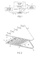
- FIGURE 1 illustrates extrusion device 10 with applicator 12 for concurrently applying two or more substantially similar and/or different materials (e.g., fluids, pastes, liquids, inks, etc.) on substrate 14.
- materials are applied through pushing and/or drawing techniques (e.g., hot and cold) in which materials are pushed (e.g., squeezed, etc.) and/or drawn (e.g., via a vacuum, etc.) through applicator 12 and out one or more dispensing openings 16 of applicator 12.
- Materials are dispensed to create one or more variously shaped entities (e.g., continuous, multi-sectional, rectangular, triangular, irregular, etc.) on substrate 14.
- Suitable entities include, but are not limited to, a bead, point, track, pipe, frame, rail, rod, seal, volume within a void, etc.
- Shape of the entity can be defined through at least one of shapes of the one or more dispensing openings 16, structure within applicator 12 (e.g., channels), characteristics of materials (e.g., viscosity, etc.), and extrusion technique (e.g., flow rate, pressure, temperature, etc.).
- Suitable materials include, but are not limited to, silver, copper, aluminum, steel, plastic, ceramic, oil, etc., combinations thereof, and/or variations thereof, including combining the above with other substances to obtain a desired density, viscosity, texture, color.
- Multiple materials can be pushed and/or pulled through applicator 12 and dispensed together to produce one or more structured layers of materials on substrate 14.
- Multiple materials can be pushed and/or pulled through applicator 12 under laminar flow to mitigate mixing of the materials.
- Mixing can be further reduced by using substantially immiscible materials, including mixing a material with one or more other materials, impurities, dopants, coatings, etc. to create pastes, etc.
- Materials can be prepared such that they are mutually insoluble, enabling striped layers to be extruded onto substrate 14 through applicator 12 with relatively little mixing. Viscosities of materials can also be matched to reduce shear and mixing between flows.
- Applicator 12 can be a nozzle, die, or any structure that receives materials and facilitates applying the materials to substrate 14. Applicator 12 can be micromachined with structures that receive and converge individual material. Applicator 12 can include N channels, where N is an integer equal to or greater than one (e.g., thousands), for merging materials within applicator 12 into a single flow dispensed by applicator 12. Each N channel can be used for introducing a different material and/or multiple channels can be used for introducing a substantially similar material. Where applicator 12 includes a single channel, the different material can be introduced through similar and/or different ports into the channel.
- Each channel can extend through a length (e.g., the entire length or a subset thereof) of applicator 12.
- one or more of the N channels can be designed to be shorter than the length of applicator 12, but relatively longer than an entrance length to produce laminar flow, wherein flow velocity is stabilized prior to merging materials. This can be achieved through known micro-machining techniques such as deep reactive ion etching, wafer bonding, etc.
- Creating applicator 12 for laminar flow mitigates and/or minimizes mixing of materials as materials traverse through applicator 12 and out of its opening.
- N channels may also be shaped to counteract effects of surface tension on materials as they progress from applicator 12 to substrate 14.
- Each channel may be uniquely and/or similarly shaped, including uniform and/or non-uniform shapes.
- applicator 12 is suitably positioned with respect to substrate 14, and the one or more materials are dispensed through applicator 12.
- Such positioning can be based on factors such as distance between applicator 12 and substrate 14, the angle of the dispensing end of applicator 12 with respect to substrate 14 (e.g., from parallel to perpendicular to substrate 14)to increase transfer efficiency, entity definition (e.g., width, height, length, diameter, etc), entity characteristics (e.g., strength, pliability, etc.), etc.
- entity definition e.g., width, height, length, diameter, etc
- entity characteristics e.g., strength, pliability, etc.
- device 10 and applicator 12 and/or substrate 14 Prior to, during, and/or after dispensing the materials on substrate 14, device 10 and applicator 12 and/or substrate 14 can be moved. For example, to create a point (or dot, ball, etc.) at a particular location on substrate 14, device 10 and applicator 12 and/or substrate 14 can be moved and suitably positioned. Subsequently, materials can be dispensed to create the point. Thereafter, device 10 and applicator 12 and/or substrate 14 can be moved to another position for a subsequent application, if any. In another example, to create a bead, device 10 and applicator 12 and/or substrate 14 can be moved to an initial position.
- FIGURE 1 depicts applicator 12 dispensing a flow of materials to form a continuous bead on substrate 14 as depicted at 18.
- the bead of material leaving applicator 12 can be quenched on substrate 14 by making substrate 14 relatively cold with respect to applicator 12, e.g., quenching component 15 can be used to cool substrate 14.
- quenching component 15 can be used to cool substrate 14.
- materials can be cured by thermal, optical and/or other means upon exit from applicator 12, e.g., curing component 17 can thermally and/or optically cure materials. If one or both materials includes ultraviolet curing agent, material can be bound up into solid form to enable further processing without mixing.
- Applicator 12 can be manufactured a variety of ways, (i) via deep silicon reactive ion etching and wafer bonding; (ii) electroplating metal up through features in a patterned resist structure; (iii) brazing together layers of etched sheet metal; (iv) generating structures out of photo-definable polymer such as SU8; (v) being machined or molded out of metal and/or plastic using conventional manufacturing techniques.
- Relative speed of motion between applicator 12 and substrate 14 and speed at which materials are dispensed determine characteristics such as whether material is stretched or compressed as it is placed on substrate 14. Rates also determine thickness and/or average thickness of extruded material. Typically, these rates are set based at least in part on one or more of application, materials, and/or substrate 14. Rates may be set to minimize separation between adjacent materials and/or deviations from desired dimensions.
- Airflow may be used to direct one or more materials onto substrate 14.Airflow around dispensing opening of applicator 12 can be provided to pull materials in desired directions. If substrate is porous, as in the case of some fuel cell electrodes, airflow (e.g., a vacuum) can be pulled through substrate 14 to increase attachment of material to substrate 14. Flow can also be controlled through controlling pressure, temperature, etc. of applicator 12 and/or substrate 14 to achieve desired flow properties of material being extruded.
- the duty cycle of each dispensed material can be controlled by adjusting a corresponding pressure of each material entering applicator 12 in which each pressure can be similar and/or different. Additionally and/or alternatively, the duty cycle can be determined by design of applicator 12. For instance, pitch of each dispensed material can be defined by geometry of applicator 12 (e.g., width of opening, number of channels, shape of channels, etc.). Both pitch and duty cycle can be configured for a particular design. In one application widths of dispensed materials may be substantially similar. With another application, width of one or more of materials may be different. In another application, one or more groups of channels may have different widths wherein channels within anyone group may have substantial similar widths. Because surface tension forces may distort pitch of material (e.g., at edges), pitch of each channel can be adjusted to compensate.
- pitch of each dispensed material can be defined by geometry of applicator 12 (e.g., width of opening, number of channels, shape of channels, etc.). Both pitch and duty cycle can be
- One or more materials can be pre-filled within one or more storage elements (not shown) associated with device 10, e.g., materials may be stored together in a similar storage element and/or separated into individual storage elements. Additionally and/or alternatively, materials may be supplied to device 10 before and/or during extrusion via one or more optional input ports (not shown) of device 10.
- Device 10 may include more than one applicator 12. Suitable configurations include, but are not limited to, a serial array of applicators 12 (e.g., staggered, adjacent, etc.), to increase a width of a single pass; stacked applicators 12, to apply multiple layers in a single pass; a matrix of applicators (serial array / stacked combination) to concurrently increase the width and the number of layers, to increase efficiency, etc. Such configurations are depicted in FIGURES 18, 19, and 20.
- a serial array of applicators 12 e.g., staggered, adjacent, etc.
- stacked applicators 12 to apply multiple layers in a single pass
- a matrix of applicators serial array / stacked combination
- Each applicator 12 may be used to dispense a plurality of materials. Substantially all of applicators 12 could dispense similar materials. Materials dispensed by one applicators 12 may be different from materials dispensed by one or more other applicators 12. Each of applicators 12 could dispense different materials, wherein materials dispensed by any one applicator 12 may be similar and/or different. Each of applicators 12 may only dispense a single material.
- Applicators 12 can be configured such that device 10 dispenses materials in an interleaved and/or adjacent manner.
- first applicator 12 dispensing K materials (where K is an integer equal to or greater than two) may dispense K adjacent materials, K materials with gaps in between, and/or some combination thereof.
- Second applicator 12 dispensing L materials (where L is an integer equal to or greater than two) may dispense L adjacent materials next to the K adjacent materials, L materials within the gaps between the K materials, and/or some combination thereof.
- Third, fourth, etc. applicator 12 can be similarly used to apply materials in connection with K and L materials.
- Device 10 can be used to create solar and/or electrochemical (e.g., fuel, battery, etc.) cell electrodes.
- Device 10 can be used to extrude lines of silver paste into high aspect ratio grid lines surrounded by sacrificial material that is in place only as long as needed to maintain the shape of the electrode on a solar cell substrate before or during any processing.
- Sacrificial material leads to an overall larger output orifice, and hence a lower pressure drop for a given material flow speed. Higher process speed is therefore achievable.
- convergent flow a minimum fabrication feature of device 10 is larger than the minimum feature of an extruded gridline.
- variations of applicator 12 can be used to additionally and/or alternatively introduce materials with vertical variation, e.g ., for introducing barrier layers onto substrate 14.
- Vertical variation can be implemented by forming channels that converge dissimilar materials together in the vertical direction within the manifold,With a solar cell application, it may be advantageous to introduce a metal bi-layer onto the cell surface with one metal making contact to the silicon as a diffusion barrier, and a second metal on top selected for either lower cost or higher conductance.
- Device 10 can be used to facilitate manufacturing light control films such as those used for computer privacy screens. Typically, such screens have a series of tall, thin opaque louver layers in a clear matrix to limit the optical transmission to a narrow range of angles. Applicator 12 could dispense alternating layers of opaque and clear materials to form a layer of louvers by molding a ridge pattern into plastic and pressing a black matrix in between the ridges, wherein the two structures can be laminated together. Device 10 can be used to print striated structures with a high aspect ratio such as artificial muscle. For instance, lateral co-extrusion in combination with a valving scheme could be used to make such structures. Multiple bands of muscle like material could be laid out in varied directions to produce a variety of actuations.
- Device 10 and applicator 12 can be used for printing. By utilizing multi-pass printing, with or without registration, systems could be developed to create thicker layers, or layers with a wider mix of materials, or functional composite materials with novel properties. Process direction can also be changed from layer to layer in order to create unique structures. For example, device 10 and applicator 12 could be used to create high strength plastics with crisscrossing grain structures similar to plywood. Device 10 and applicator 12 enables printing a wide range of materials with viscosities up to the order several hundred thousand cP, with high aspect ratios on the order of 10:1 and features as small as 100 nanometers.
- Employing applicator 12 can reduce costs. Typical costs associated with fabricating electrodes of a fuel cell can be reduced $10 to $20 per square foot of electrode area.
- a wide array of materials ranging from paints, waxes, colloidal suspensions, pastes, resists, particle suspensions, gels, thixotropic materials, etc. can be extruded through applicator 12. Materials are not limited by viscosity and/or by need to form a vapor, and more than one material can be dispensed simultaneously.
- Convergent applicator 12 can produce feature sizes with lateral dimensions on the order of 100 nanometers. Thickness of a layer (e.g., about 50 microns) can be variously applied and, large volumes of material can be printed in single pass. The printed mark would essentially become a 2D feature if the surface was to get wet.
- Applicator 12 can apply pastes to render three dimensional (3D) structures with relatively high aspect ratio, typically 2:1 or greater, for example, 10:1 for fuel cell applications.
- Productivity of a co-extrusion process typically depends on dispense rate of fluids and for a fixed nozzle pressure, dispense rate is lower for fluids of higher viscosity. To achieve high process throughput, low viscosity is desired. On the other hand, to produce co-extruded composite material with well defined interfaces and overall shape that follows the nozzle geometry, high viscosity is desired.
- One way to achieve high nozzle throughput and shape retention is to dispense shear-thinning fluids. Such, non-Newtonian fluids, generally lower their viscosity in the presence of shear stress, sometimes by large amounts, even by factors of 100 in some cases for example as described in Rao et al., Adv. Materials vol. 17 no. 3 (2005 ).
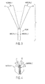
- FIGURE 2 illustrates an applicator that can be used as applicator 12 of device 10.
- the applicator includes manifold 20 having a first side 22 and second side 24.
- Manifold 20 can be fabricated by known micro-machining techniques such as deep reactive ion etching and wafer bonding, for example.
- Each of halves 22 and 24 include M channels 26, wherein M is an integer equal to or greater than one (e.g., thousands or more). For clarity, ten channels are shown.
- Channels 26 typically are machined to extend a defined length of manifold 20, e.g ., channels 26 may be fabricated to be relatively longer than an entrance length to create laminar flow, but less then the entire length of manifold 20.
- Channels 26 can also be machined to create similar and/or different shaped uniform and/or non-uniform channels.
- each of channels 26 forms one or more isolated compartments, conduits, passageways, etc. beginning at first end 28 of manifold 20 and extending toward second end 30 of manifold 20 up to region 32 where channels 26 terminate and converge into single volume 34.
- compartments, conduits, passageways, etc. formed by channels 26 may not be isolated such that materials flowing through adjacent channels may come into contact with each other.
- Manifold 20 further includes ports for receiving materials.
- a plurality of ports 36 can be interleaved and located on first side 22, and a plurality of ports 38 can be interleaved and located on second side 24.
- the ports 36 and 38 can all be located on one and/or both of sides 22 and 24 of manifold 20.
- a single material may be fed into ports 36 and 38 or a different material may be fed into each of ports 36 and 38.
- one or more materials may be fed into ports 36 on first side 22 of manifold 20, and one or more different materials may be fed into ports 38 on second side 24 of manifold 20.
- materials traversing through channels 26 and merging in region 34 typically do not mix or there is relatively minimal mixing of materials. Viscosities of materials can be matched to reduce shear and mixing between materials.
- channels 26 may be shaped to counteract effects of surface tension on material as it progresses out of manifold 20.
- Manifold 20 and/or M channels 26 can be variously shaped to facilitate producing laminar flow, merging different materials, and/or producing a desired shape on substrate 14.
- a suitable manifold shape includes a trapezoidal shape with channels extending and/or tapering from first end 28 of manifold 20 to second end 30 of the manifold.
- FIGURES 3 and 4 illustrate another applicator that can be used as applicator 12 of device 10,, where separate structures are used to dispense each material.
- Dispenser 40 is used to apply a first material
- dispenser 42 is used to apply Zth material, wherein Z is an integer equal to or greater than one.
- Dispensers 40 and 42 can be positioned relative to each other by micro-positioners and/or other suitable drives. Alignment from channel-to-channel can also be achieved by interlocking features built into dispensers 40 and 42, such as comb-like structures. Since the materials come into contact outside of dispensers 40 and 42, materials can be partially intermixable if the materials can be cured relatively rapidly after being dispensed onto substrate 14 (e.g. UV-curing). Materials can be co-mingled into a layer in flight between channel tips and substrate 14. Alternately, separate stripes on substrate 14 may flow together once materials are deposited on substrate 14.
- FIGURE 4 shows each of dispensers 40 and 42 can include one or more dispensing ports.
- Dispenser ports 44 are used to apply the first material
- dispenser ports 46 are used to apply Zth material.
- Ports 44 can be separated by a plurality of (equal or non-equal) gaps 48 for applying a plurality of flows of first material.
- Ports 44 can be offset parallel to ports 44 and separated by a plurality of (equal or non-equal) gaps 50 in order to facilitate dispensing Zth material in gaps 44 to render a flow comprising alternating materials with a width based on an aggregate number of ports 44 and 46.
- FIGURE 5 illustrates another configuration of an applicator that can be used as applicator 12.
- the applicator is used to apply two different materials on substrate 14.
- the applicator includes manifold 20, which includes a plurality of channels 26 that are fabricated to facilitate creating laminar flow to merge materials received in each channel 26 within manifold 20 into a single flow of separate materials (with material to material contact) while mitigating mixing of the materials.
- Channels 26 are associated with either ports 36 or ports 38, which are used to introduce at least one of the materials into manifold 20. Two such ports are illustrated.
- the two different materials are introduced into manifold 20 in an interleaved manner such that adjacent channels 26 are used for different materials.
- similar materials can be introduced into adjacent channels.
- two different materials can be introduced into manifold 20 from opposing sides 52 and 54.
- two different materials can be introduced from a substantially similar side(s) (e.g., either side 52 or side 54), including introducing both materials from multiple sides (e.g., both side 52 and side 54).
- the side in which a material is introduced may be arbitrary or defined in order to establish a particular sequence.
- a first material is supplied to some of channels 26 of manifold 20 through one or more of the plurality of ports 38, and another material is supplied to different channels 26 of manifold 20 through the plurality of ports 36.
- the relative position of ports 36 and 38 with respect to each other can be arbitrary such that manifold 20 could be turned 180 degrees.
- materials traverse (e.g., via a push, a pull, etc. technique) through corresponding channels and merge under laminar flow within manifold 20 to form a single flow of materials.
- the applicator further includes housing 56, which reinforces the exterior of the applicator.
- Housing 56 can be designed to taper, or diminish in size (e.g., thickness, diameter, width, etc.) from back region 58 to front region 60.
- Such tapering provides relatively more support at back region 58, which typically includes the highest pressure regions of the applicator, while enabling dispensing end 62 to be positioned adjacent to and/or in contact with substrate 14.
- Such positioning can be based on factors such as distance between the applicator and substrate 14, the angle of dispensing end 62 with respect to substrate 14, etc.
- the applicator and/or substrate 14 can be moved in order facilitate applying the materials to substrate 14.
- Relatively narrower dispensing end 62 enables multiple applicators to be arrayed together in a staggered or non-staggered arrangement to increase width of material applied with each pass of the applicators across substrate 14.
- Substrate 14 can be fed as cut sheets or in a roll-to-roll process.
- Flow speed of the material can be controlled as described above. For example, pressure of the materials can be suitably adjusted to effectuate flow speed.
- FIGURE 6 illustrates a portion of a photovoltaic cell, such as a solar cell, with grid lines created via applicator 12.
- the photovoltaic cell includes semiconductor 64 with p-type region 66 and n-type region 68.
- regions 66 and 68 of semiconductor 64 can be formed from semiconductor materials such as, for example, Aluminium Arsenide, Aluminium Gallium Arsenide, Boron Nitride, Cadmium Sulfide, Cadmium Selenide, Diamond, Gallium Arsenide, Gallium Nitride, Germanium, Indium Phosphide, Silicon, Silicon Carbide, Silicon Germanium, Silicon on insulator, Zinc Sulfide, Zinc Selenide, etc.
- An electric field is created across p-n junction 70 and allows electrons and/or holes to flow from one region to another region of semiconductor 64, for example, upon absorption of a photon. Electrons pass from n-type region 68 into p-type region 66, and holes pass from p-type region 66 to n-type region 68.
- the photovoltaic cell further includes contact 72 formed adjacent to side 74 of p-type region 66.
- Contact 72 can be formed via metal paste such as aluminum based paste.
- Grid contact 76 is formed adjacent to side 78 of n-type region 68.
- Grid contact 76 includes conducting fingers 80 separated by non-conducting regions 82.
- Fingers 80 can be formed via a metal paste such as silver based paste.
- Contacts 72 and/or 76 may be exposed to heat treatment, and/or drying, curing, and/or sintering, and/or other processes.
- a plurality of the cells can be interconnected in series and/or parallel, for example, via flat wires or metal ribbons, and assembled into modules or panels.
- a sheet of tempered glass (not shown) may be layered over grid contact 76 and/or a polymer encapsulation (not shown) may be formed over contacts 72.
- the photon absorbing surface may include a textured surface and/or be coated with antireflection material (e.g., silicon nitride, titanium dioxide, etc.) in order to increase the amount of light absorbed into the cell.
- Grid contract 76 can be formed as rectangular bars or variously shaped, for example, as triangular volumes (e.g., with the point of the triangle facing away from the semiconductor 64) that facilitate directing photons into semiconductor 64 and mitigating blocking photons from entering semiconductor 64, which can improve efficiency and/or generation of electrical power.
- Electrode 84 can be connected to grid contacts 76 and external load 86, and electrode 88 can be connected to external load 86 and contact 72.
- photons 90 When photons 90 are absorbed into semiconductor 64, their energy excites electrons therein, which subsequently freely move. Electrical current is generated when excited electrons in n-type region 68 travel through grid contact 76 and electrode 84 to external load 86 and back through electrode 88 and contact 72 to p-type region 72.
- FIGURE 7 illustrates a method for fabricating grid lines on a photovoltaic device such as the photovoltaic cell described in connection with FIGURE 6.
- a semiconductor is formed, which can include various semiconductor materials.
- the semiconductor can be formed by coupling a piece of n-type silicon with a piece of p-type silicon to form a semiconductor p-n junction, or an n-type dopant (e.g., Phosphorus, Arsenic, Antimony, etc.) or a p-type dopant (e.g., Boron, etc.) is diffused into a side of a silicon wafer, or naturally occurring semiconductors such as blue diamonds, which contain Boron impurities, can be used.
- an n-type dopant e.g., Phosphorus, Arsenic, Antimony, etc.
- a p-type dopant e.g., Boron, etc.
- the photovoltaic cells can be coupled in a serial and/or parallel manner to create a photovoltaic module or panel.
- a conducting contact is formed adjacent to the p-type region.
- a conducting grid is formed adjacent to the n-type region. In one example, device 10, as described above, is used to form the conducting grid.
- electrodes are coupled from the conducting contact and the conducting grid to a load. When photons are absorbed into the semiconductor, electrical energy is generated via the photovoltaic effect.
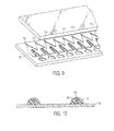
- FIGURE 8 illustrates a method for fabricating grid lines in connection with FIGURE 6.
- one or more applicators e.g., applicators 12
- the applicators can be coupled in a serial (e.g., staggered or non-staggered) and/or parallel manner.
- the device can be suitably positioned with respect to a surface of the photovoltaic substrate.
- silver paste and sacrificial material are fed into applicators.
- the silver paste and sacrificial materials can be pushed and/or drawn into the applicators through known techniques.
- Each of the applicators can include a plurality of channels fabricated to facilitate producing laminar flow for merging materials within the applicators while mitigating mixing of such materials.
- Silver paste and sacrificial material typically are fed in an interleaved manner such that adjacent channels are fed different materials (e.g., one channel is fed silver paste while an adjacent channel is fed the sacrificial material), or alternating channels are fed a similar material (e.g., every odd channel or every even channel is fed is either silver paste or sacrificial material).
- materials traverse through their respective channels.
- Parameters such as rate, temperature, duty cycle, etc. are set based at least in part on factors such as material viscosity and/or desired characteristics such as grid line length, width, strength, resistance, etc. These parameters are set to produce a laminar flow for each material traveling through each of the channels.
- a plurality of flows from the plurality of channels within each applicator is merged into a single flow of alternating materials. Since each flow is a laminar flow, the materials merge with reduced mixing relative to non-laminar flows.
- the sacrificial material is preferably, but is not limited to, a material with a closely matched rheology to that of the silver paste.
- merged materials are dispensed from each of the applicators and applied to the photovoltaic substrate to create grid lines.
- the device and applicators and/or photovoltaic substrate can be moved relative to the other, and can be used multiple times in order to create a desired width and/or apply a desired number of layers, for example, for introducing barrier layers onto the photovoltaic substrate like a metal bi-layer with one metal making contact with the substrate as a diffusion barrier and another metal formed over it to reduce cost and/or increase conductance.
- Grid lines can be further processed, for example, via heat treatment or sintering to make Ohmic contact with the substrate.
- applicator 12 for the grid lines results in grid lines with a high aspect ratio such as up to about 10:1 and relatively fine features such as less than about 5 to 10 microns.
- grid lines cover about 4% of the area and are opaque and metallic and, thus, block photons from entering semiconductor 64.
- the high aspect ratio fine feature grid lines produced via applicator 12 take up less than 4% of the area and allow more photons to enter semiconductor 64, which improves electrical power output. Because narrow grid lines have a smaller metal-to-semiconductor contact area, a beneficial effect of reducing electron-hole recombination is obtained.
- FIGURE 9 illustrates an exploded view of a portion of a co-extrusion/dispense applicator suitable for the deposition of solar cell gridlines.
- the applicator includes an array of outlets 112.
- Each of outlets 112 corresponds to a single gridline and dispenses a material composite consisting of a central metal line of high aspect ratio with supporting material adjacent to one or more sides of the metal line.
- FIGURE 10 depicts a cross section of two such gridlines dispensed via the applicator of FIGURE 9 on substrate 120.
- Each of the dispensed gridlines includes metal line 116 and support material 118.
- convergent path 120 leading to each outlet 112 has advantages in comparison to a straight channel.
- the extruded features can be finer than the finest minimum design feature of the applicator itself.
- the applicator uses less material to support the gridline compared to one that uses a single outlet.
- a co-extrusion applicator with the estimated parameters illustrated in Table 1 could be used to dispense materials to make gridlines on a crystalline silicon solar cell.
- Table 1 Exemplary applicator parameters for generating a gridline. Sheet Thickness 152 microns Gridline Pitch 2.5 mm Applicator Speed 1 cm/sec Past Viscosity 100,000 Cp Applicator Angle 45 degrees Applicator Exit Width 304.8 Microns Silver Width 49.2 microns Silver Line Cross Section 7,500 microns ⁇ 2 Silver Line Aspect Ratio 3.10:1 Silver Flow 0.075 mm ⁇ 3/sec Applicator Compression 6.2:1 Applicator Pressure Drop 2.24 atm
- convergent channels are patterned into a sheet of material with a thickness of approximately 0.15 mm.
- Output orifices of the applicator/nozzles are repeated on a pitch of 2.5 mm.
- paste of 1000 poise is ejected at a rate of 1 cm/sec.
- the central stripe of silver is approximately 50 microns wide with an aspect ratio of 3.1.
- An applicator/nozzle with many separate outputs may have inherent instability, particularly fluid being dispensed undergoes large amounts of shear thinning. This instability could cause fluids in different channels to divide into different flow states. The flows could divide into low flow, low shear, high viscosity state in some channels while others have a high flow, high shear, low viscosity state.
- An undesirable condition is one in which given fluid displacement rate, overall pressure drop is lowest for a combination of high and low output flows.
- One way to avoid uneven flows from a dispense nozzle with multiple outputs (such as the applicator of FIGURE 9) is to drive each output from a separate fluid pump. A particularly desirable and cost effective way to achieve this is to create an array of positive displacement pumps in which fluid in multiple reservoirs is simultaneously compressed by a single actuator, such as a motor and lead screw driving a plate with multiple plungers.
- FIGURE 11 illustrates such an applicator in which a channel includes two or more sub-channels 122 positioned vertically with respect to each other to generate vertically layered entity 124 via exit port outlet 126. Each of the sub-channels includes inlet 128 for introducing a material.
- the applicator can include a plurality of the channels with a similar and/or different number of sub-channels 122 to concurrently form horizontal and vertical layers. The foregoing structure facilitates lowering metallization cost of solar cells.
- vertically layered entity 124 includes a comparatively expensive contact material 130 such as a silver gridline metallization formed adjacent to substrate 132.
- a layer such as a nickel metallization that acts as diffusion barrier 134 is formed vertically adjacent to contact material 130.
- metal line 136 such as a layer of copper metallization that serves as an additional low cost material to carry current generated by the solar cell.
- Support material 138 is formed horizontally adjacent to contact material 130, diffusion barrier 134, and/or metal line 136.
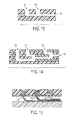
- FIGURE 13 vertical flows through sub-channels 122 can be simply merged together and dispensed at the outlet 126 as shown. Alternatively, sub-channels 122 can converge together in order to produce finer features and to lessen to total pressure drop for a given flow rate.
- FIGURE14 one layer of a stack of bonded plates is shown. On this layer, flows through sub-channels 122 converge vertically. Layers above and below may contain filling orifices. Additional layers above and below can be introduced and merge the laterally disposed flows of sacrificial material.
- FIGURE 16 illustrates an exemplary fuel cell anode with at least one channel created via applicator of FIGURE 9.
- the applicator of FIGURE 9 can be used to create barrier channels and/or electrodes for other electrochemical devices such a batteries (e.g., zinc-air), etc.
- the fuel cell anode includes a porous electrode and gas diffusion layer 144, membrane 146 consisting of for example phosphoric acid bound in a polymer structure, and composite porous electrode 148 disposed there between.
- Electrode 144 typically is a porous electrode and gas diffusion layer which allows reactants, such as oxygen for a hydrogen fuel cell, to permeate into composite porous electrode 148, consisting of alternating vertical stripes of nanoporous hydrophobic material (e.g., polytetrafluoroethylene particles) 150 and nanoporous phdrophilic conductor and catalyst 152 (e.g., graphite particles and platinum).
- a catalyst, such as platinum, in conductor lines 152 catalyzes the reaction to produce water.
- the reaction is characterized by the following: H + + 1 2 ⁇ O 2 + e - ⁇ ⁇ Pt ⁇ H 2 ⁇ O .
- the porous nature of the stripes 150 and 152 provide for continuous replenishment of the reactants consumed within the composite porous electrode 148.
- Relatively high aspect ratio (10:1) thin feature (5-10 microns) porous lines are desirable because they produce a long reaction zone that increases utilization of the expensive catalyst needed for the electrode.
- conventional extrusion techniques cannot fabricate such lines on relatively rough (0.01 mm RMS) substrates at costs below $1/square foot.
- the structure should facilitate conducting protons form the membrane to the reaction site, diffusing oxygen to the reaction site with low partial pressure drop, conducting electrons from the porous electrode to the reaction site, carry heat away from the reaction site, and withstand a compressive mechanical load of 100-200 PSI.
- the challenges imposed by the electrode structure and its target cost place nearly impossible demands on conventional photolithographic, direct marking, and molding techniques.
- FIGURE 17 illustrates a method for fabricating the membrane electrode assembly of the fuel cell described in FIGURE 16.
- a device employing the applicator of FIGURE 9 with respect to a surface of a substrate.
- Such positioning includes a distance between dispensing ends of the applicators and the photovoltaic device, an angle of the dispensing ends of the applicators with respect to the photovoltaic substrate, etc.
- a first material for creating hydrophilic lines, and a second material for creating hydrophobic lines are fed into the applicator(s).
- Each of the applicators can include a plurality of channels fabricated to facilitate producing laminar flow for merging materials within the applicators while mitigating mixing of such materials.
- the first and second materials typically are fed in an interleaved manner such that adjacent channels are fed different materials, or alternating channels are fed a similar material.
- Parameters such as rate, temperature, duty cycle, etc. are set based at least in part on factors such as material viscosity and/or desired characteristics such as grid line length, width, strength, resistance, etc. These parameters are set to produce a laminar flow for each material traveling through each of the channels.
- a plurality of flows from a plurality of channels within each applicator is merged into a single flow of alternating materials. Since each flow is a laminar flow, the materials merge with reduced mixing relative to non-laminar flow flows.
- the merged materials are dispensed from the applicator(s) to create a plurality of channels the form the electrolyte.
- the applicator(s) and/or substrate can be moved relative to the other.
- the applicator(s) can be used multiple times in order to create a desired width and/or apply a desired number of layers.
- the materials can be formulated such that they are substantially immiscible.
- Particles that form the network of porous media in the electrode can be coated, if necessary, with hydrophilic or hydrophobic coatings to affect their intermixing. Both pairs and combinations of liquids and colloidal suspensions can be made to be mutually insoluble, enabling striped layers of these materials to be extruded onto the substrate through the applicator without substantial mixing.
- Table 2 provides examples of throughput related parameters for the applicators described herein.
- the throughput related parameters were obtained by estimating a pressure gradient to produce a Poiseuille flow in a rectangular cross section at various points along a length of applicator 12.
- a relatively highly viscous material could be printed at a rate of about 1 square foot per minute.
- Injector pitch at the wide end of the applicator is about 50 microns, and width converges from about 50 mm to about 5 mm, with about 1000 injection ports, and a printed pitch at the applicator opening of about 5 microns.
- Height of the layer deposited by the applicator is about 50 microns, whereas the applicator channel is about 200 microns deep.
- the deposited layer is thinned by stretching, or moving the substrate faster (e.g., about four-times) than flow rate of materials as they leave the applicator.
- applicator channel is about 500 microns deep, and layer thickness is about 50 microns, a substantially similar print speed can be achieved with a pressure drop of only about 1.7 PSI.
- the applicator can include more injection ports or a narrower opening.
Landscapes
- Engineering & Computer Science (AREA)
- Mechanical Engineering (AREA)
- Manufacturing & Machinery (AREA)
- Coating Apparatus (AREA)
- Extrusion Moulding Of Plastics Or The Like (AREA)
- Application Of Or Painting With Fluid Materials (AREA)
- Photovoltaic Devices (AREA)
- Inert Electrodes (AREA)
Abstract
Description
- The following relates to micro-extrusion systems and methods for co-extruding multiple similar and/or dissimilar materials to form relatively fine structures with relatively high aspect ratios.
- Conventional techniques cannot render relatively high aspect-ratio (e.g., 10:1) fine featured (e.g., less then 5 micron) porous (e.g., 0.01 mm RMS) structures for costs below $1/sq. ft. Thus, extrusion typically is not used for creating conducting contacts and/or channels for electrochemical (e.g., fuel), solar, and/or other types of cells, which leverage high aspect-ratio fine featured porous structures to increase efficiency and electrical power generation.
- In one aspect, a device for extruding/dispensing materials on a substrate is illustrated. The device includes a housing enclosing at least two channels. The at least two channels are formed to facilitate flow and each channel includes at least one entrance port for accepting a different material. The device further includes an exit port for co-extruding the materials on the substrate to generate a relatively fine feature with a relatively high aspect ratio.
- FIGURE 1 illustrates an extrusion device with an applicator for concurrently applying one or more materials on a substrate;
- FIGURE 2 illustrates an exemplary applicator;
- FIGURE 3 illustrates another exemplary applicator;
- FIGURE 4 illustrates a plurality of dispensing ports;
- FIGURE 5 illustrates another exemplary applicator;
- FIGURE 6 illustrates an exemplary portion of a photovoltaic cell;
- FIGURE 7 illustrates a method for fabricating the photovoltaic cell;
- FIGURE 8 illustrates a method for fabricating grid lines;
- FIGURE 9 illustrates an exploded view of a portion of an exemplary applicator;
- FIGURE 10 illustrates a cross section of gridlines;
- FIGURE 11 illustrates a portion of an exemplary applicator with vertically positioned sub-channels for creating vertically layered entities;
- FIGURE 12 illustrates a cross section of gridlines;
- FIGURE 13 illustrates alternative configuration for producing a vertically layered entity in which flows are vertically merged and dispensed;
- FIGURE 14 illustrates alternative configuration for producing a vertically layered entity in which flows are vertically merged together pair-wise;
- FIGURE 15 illustrates alternative configurations for producing vertically layered entities in which flows are vertically merged together external to the applicator;
- FIGURE 16 illustrates a portion of an exemplary fuel cell;
- FIGURE 17 illustrates a method for fabricating the electrode of the fuel cell described in FIGURE 13;
- FIGURE 18 illustrates a serial array of applicators;
- FIGURE 19 illustrates stacked applicators; and
- FIGURE 20 illustrates a matrix of applicators.
- FIGURE 1 illustrates
extrusion device 10 with applicator 12 for concurrently applying two or more substantially similar and/or different materials (e.g., fluids, pastes, liquids, inks, etc.) onsubstrate 14. Materials are applied through pushing and/or drawing techniques (e.g., hot and cold) in which materials are pushed (e.g., squeezed, etc.) and/or drawn (e.g., via a vacuum, etc.) through applicator 12 and out one or more dispensingopenings 16 of applicator 12. Materials are dispensed to create one or more variously shaped entities (e.g., continuous, multi-sectional, rectangular, triangular, irregular, etc.) onsubstrate 14. Suitable entities include, but are not limited to, a bead, point, track, pipe, frame, rail, rod, seal, volume within a void, etc. Shape of the entity can be defined through at least one of shapes of the one or more dispensingopenings 16, structure within applicator 12 (e.g., channels), characteristics of materials (e.g., viscosity, etc.), and extrusion technique (e.g., flow rate, pressure, temperature, etc.). Suitable materials include, but are not limited to, silver, copper, aluminum, steel, plastic, ceramic, oil, etc., combinations thereof, and/or variations thereof, including combining the above with other substances to obtain a desired density, viscosity, texture, color. - Multiple materials (e.g., with viscosity from about 1 centipoise (cP) to about several hundred thousand cP) can be pushed and/or pulled through applicator 12 and dispensed together to produce one or more structured layers of materials on
substrate 14. Multiple materials can be pushed and/or pulled through applicator 12 under laminar flow to mitigate mixing of the materials. Mixing can be further reduced by using substantially immiscible materials, including mixing a material with one or more other materials, impurities, dopants, coatings, etc. to create pastes, etc. Materials can be prepared such that they are mutually insoluble, enabling striped layers to be extruded ontosubstrate 14 through applicator 12 with relatively little mixing. Viscosities of materials can also be matched to reduce shear and mixing between flows. - Applicator 12 can be a nozzle, die, or any structure that receives materials and facilitates applying the materials to
substrate 14. Applicator 12 can be micromachined with structures that receive and converge individual material. Applicator 12 can include N channels, where N is an integer equal to or greater than one (e.g., thousands), for merging materials within applicator 12 into a single flow dispensed by applicator 12. Each N channel can be used for introducing a different material and/or multiple channels can be used for introducing a substantially similar material. Where applicator 12 includes a single channel, the different material can be introduced through similar and/or different ports into the channel. - Each channel can extend through a length (e.g., the entire length or a subset thereof) of applicator 12. For instance, one or more of the N channels can be designed to be shorter than the length of applicator 12, but relatively longer than an entrance length to produce laminar flow, wherein flow velocity is stabilized prior to merging materials. This can be achieved through known micro-machining techniques such as deep reactive ion etching, wafer bonding, etc. Creating applicator 12 for laminar flow mitigates and/or minimizes mixing of materials as materials traverse through applicator 12 and out of its opening. N channels may also be shaped to counteract effects of surface tension on materials as they progress from applicator 12 to
substrate 14. Each channel may be uniquely and/or similarly shaped, including uniform and/or non-uniform shapes. - To deposit the entity (e.g., bead, point, etc.) onto
substrate 14, applicator 12 is suitably positioned with respect tosubstrate 14, and the one or more materials are dispensed through applicator 12. Such positioning can be based on factors such as distance between applicator 12 andsubstrate 14, the angle of the dispensing end of applicator 12 with respect to substrate 14 (e.g., from parallel to perpendicular to substrate 14)to increase transfer efficiency, entity definition (e.g., width, height, length, diameter, etc), entity characteristics (e.g., strength, pliability, etc.), etc. Such positioning may result in contact between applicator 12 andsubstrate 14. FIGURE 1 depicts applicator 12 positioned abovesubstrate 14 during dispensing. - Prior to, during, and/or after dispensing the materials on
substrate 14,device 10 and applicator 12 and/orsubstrate 14 can be moved. For example, to create a point (or dot, ball, etc.) at a particular location onsubstrate 14,device 10 and applicator 12 and/orsubstrate 14 can be moved and suitably positioned. Subsequently, materials can be dispensed to create the point. Thereafter,device 10 and applicator 12 and/orsubstrate 14 can be moved to another position for a subsequent application, if any. In another example, to create a bead,device 10 and applicator 12 and/orsubstrate 14 can be moved to an initial position. During dispensing of materials onsubstrate 14,device 10 and applicator 12 and/orsubstrate 14 can be moved in a direction to facilitate forming the bead onsubstrate 14. FIGURE 1 depicts applicator 12 dispensing a flow of materials to form a continuous bead onsubstrate 14 as depicted at 18. - To limit the tendency for materials to intermix after extrusion, the bead of material leaving applicator 12 can be quenched on
substrate 14 by makingsubstrate 14 relatively cold with respect to applicator 12, e.g.,quenching component 15 can be used to coolsubstrate 14. In another technique, materials can be cured by thermal, optical and/or other means upon exit from applicator 12, e.g., curingcomponent 17 can thermally and/or optically cure materials. If one or both materials includes ultraviolet curing agent, material can be bound up into solid form to enable further processing without mixing. - Applicator 12 can be manufactured a variety of ways, (i) via deep silicon reactive ion etching and wafer bonding; (ii) electroplating metal up through features in a patterned resist structure; (iii) brazing together layers of etched sheet metal; (iv) generating structures out of photo-definable polymer such as SU8; (v) being machined or molded out of metal and/or plastic using conventional manufacturing techniques.
- Relative speed of motion between applicator 12 and
substrate 14 and speed at which materials are dispensed determine characteristics such as whether material is stretched or compressed as it is placed onsubstrate 14. Rates also determine thickness and/or average thickness of extruded material. Typically, these rates are set based at least in part on one or more of application, materials, and/orsubstrate 14. Rates may be set to minimize separation between adjacent materials and/or deviations from desired dimensions. Airflow may be used to direct one or more materials onto substrate 14.Airflow around dispensing opening of applicator 12 can be provided to pull materials in desired directions. If substrate is porous, as in the case of some fuel cell electrodes, airflow (e.g., a vacuum) can be pulled throughsubstrate 14 to increase attachment of material tosubstrate 14. Flow can also be controlled through controlling pressure, temperature, etc. of applicator 12 and/orsubstrate 14 to achieve desired flow properties of material being extruded. - The duty cycle of each dispensed material can be controlled by adjusting a corresponding pressure of each material entering applicator 12 in which each pressure can be similar and/or different. Additionally and/or alternatively, the duty cycle can be determined by design of applicator 12. For instance, pitch of each dispensed material can be defined by geometry of applicator 12 (e.g., width of opening, number of channels, shape of channels, etc.). Both pitch and duty cycle can be configured for a particular design. In one application widths of dispensed materials may be substantially similar. With another application, width of one or more of materials may be different. In another application, one or more groups of channels may have different widths wherein channels within anyone group may have substantial similar widths. Because surface tension forces may distort pitch of material (e.g., at edges), pitch of each channel can be adjusted to compensate.
- One or more materials can be pre-filled within one or more storage elements (not shown) associated with
device 10, e.g., materials may be stored together in a similar storage element and/or separated into individual storage elements. Additionally and/or alternatively, materials may be supplied todevice 10 before and/or during extrusion via one or more optional input ports (not shown) ofdevice 10. -
Device 10 may include more than one applicator 12. Suitable configurations include, but are not limited to, a serial array of applicators 12 (e.g., staggered, adjacent, etc.), to increase a width of a single pass; stacked applicators 12, to apply multiple layers in a single pass; a matrix of applicators (serial array / stacked combination) to concurrently increase the width and the number of layers, to increase efficiency, etc. Such configurations are depicted in FIGURES 18, 19, and 20. - Each applicator 12 may be used to dispense a plurality of materials. Substantially all of applicators 12 could dispense similar materials. Materials dispensed by one applicators 12 may be different from materials dispensed by one or more other applicators 12. Each of applicators 12 could dispense different materials, wherein materials dispensed by any one applicator 12 may be similar and/or different. Each of applicators 12 may only dispense a single material.
- Applicators 12 can be configured such that
device 10 dispenses materials in an interleaved and/or adjacent manner. Thus, first applicator 12 dispensing K materials (where K is an integer equal to or greater than two) may dispense K adjacent materials, K materials with gaps in between, and/or some combination thereof. Second applicator 12 dispensing L materials (where L is an integer equal to or greater than two) may dispense L adjacent materials next to the K adjacent materials, L materials within the gaps between the K materials, and/or some combination thereof. Third, fourth, etc. applicator 12 can be similarly used to apply materials in connection with K and L materials. -
Device 10 can be used to create solar and/or electrochemical (e.g., fuel, battery, etc.) cell electrodes.Device 10 can be used to extrude lines of silver paste into high aspect ratio grid lines surrounded by sacrificial material that is in place only as long as needed to maintain the shape of the electrode on a solar cell substrate before or during any processing. Sacrificial material leads to an overall larger output orifice, and hence a lower pressure drop for a given material flow speed. Higher process speed is therefore achievable. When convergent flow is used a minimum fabrication feature ofdevice 10 is larger than the minimum feature of an extruded gridline. - In addition to striped materials with a lateral variation, variations of applicator 12 can be used to additionally and/or alternatively introduce materials with vertical variation, e.g., for introducing barrier layers onto
substrate 14. Vertical variation can be implemented by forming channels that converge dissimilar materials together in the vertical direction within the manifold,With a solar cell application, it may be advantageous to introduce a metal bi-layer onto the cell surface with one metal making contact to the silicon as a diffusion barrier, and a second metal on top selected for either lower cost or higher conductance. -
Device 10 can be used to facilitate manufacturing light control films such as those used for computer privacy screens. Typically, such screens have a series of tall, thin opaque louver layers in a clear matrix to limit the optical transmission to a narrow range of angles. Applicator 12 could dispense alternating layers of opaque and clear materials to form a layer of louvers by molding a ridge pattern into plastic and pressing a black matrix in between the ridges, wherein the two structures can be laminated together.Device 10 can be used to print striated structures with a high aspect ratio such as artificial muscle. For instance, lateral co-extrusion in combination with a valving scheme could be used to make such structures. Multiple bands of muscle like material could be laid out in varied directions to produce a variety of actuations. -
Device 10 and applicator 12 can be used for printing. By utilizing multi-pass printing, with or without registration, systems could be developed to create thicker layers, or layers with a wider mix of materials, or functional composite materials with novel properties. Process direction can also be changed from layer to layer in order to create unique structures. For example,device 10 and applicator 12 could be used to create high strength plastics with crisscrossing grain structures similar to plywood.Device 10 and applicator 12 enables printing a wide range of materials with viscosities up to the order several hundred thousand cP, with high aspect ratios on the order of 10:1 and features as small as 100 nanometers. - Employing applicator 12 can reduce costs. Typical costs associated with fabricating electrodes of a fuel cell can be reduced $10 to $20 per square foot of electrode area. A wide array of materials ranging from paints, waxes, colloidal suspensions, pastes, resists, particle suspensions, gels, thixotropic materials, etc. can be extruded through applicator 12. Materials are not limited by viscosity and/or by need to form a vapor, and more than one material can be dispensed simultaneously. Convergent applicator 12 can produce feature sizes with lateral dimensions on the order of 100 nanometers. Thickness of a layer (e.g., about 50 microns) can be variously applied and, large volumes of material can be printed in single pass. The printed mark would essentially become a 2D feature if the surface was to get wet. Applicator 12 can apply pastes to render three dimensional (3D) structures with relatively high aspect ratio, typically 2:1 or greater, for example, 10:1 for fuel cell applications.
- Productivity of a co-extrusion process typically depends on dispense rate of fluids and for a fixed nozzle pressure, dispense rate is lower for fluids of higher viscosity. To achieve high process throughput, low viscosity is desired. On the other hand, to produce co-extruded composite material with well defined interfaces and overall shape that follows the nozzle geometry, high viscosity is desired. One way to achieve high nozzle throughput and shape retention is to dispense shear-thinning fluids. Such, non-Newtonian fluids, generally lower their viscosity in the presence of shear stress, sometimes by large amounts, even by factors of 100 in some cases for example as described in Rao et al., Adv. Materials vol. 17 no. 3 (2005).
- FIGURE 2 illustrates an applicator that can be used as applicator 12 of
device 10. - The applicator includes
manifold 20 having afirst side 22 andsecond side 24.Manifold 20 can be fabricated by known micro-machining techniques such as deep reactive ion etching and wafer bonding, for example. Each ofhalves channels 26, wherein M is an integer equal to or greater than one (e.g., thousands or more). For clarity, ten channels are shown.Channels 26 typically are machined to extend a defined length ofmanifold 20, e.g.,channels 26 may be fabricated to be relatively longer than an entrance length to create laminar flow, but less then the entire length ofmanifold 20.Channels 26 can also be machined to create similar and/or different shaped uniform and/or non-uniform channels. -
Sides sides channels 26 forms one or more isolated compartments, conduits, passageways, etc. beginning atfirst end 28 ofmanifold 20 and extending towardsecond end 30 ofmanifold 20 up toregion 32 wherechannels 26 terminate and converge intosingle volume 34. In other instances, compartments, conduits, passageways, etc. formed bychannels 26 may not be isolated such that materials flowing through adjacent channels may come into contact with each other. -
Manifold 20 further includes ports for receiving materials. As depicted, a plurality ofports 36 can be interleaved and located onfirst side 22, and a plurality ofports 38 can be interleaved and located onsecond side 24. In other instances, theports sides manifold 20. A single material may be fed intoports ports ports 36 onfirst side 22 ofmanifold 20, and one or more different materials may be fed intoports 38 onsecond side 24 ofmanifold 20. - Different materials traverse through
respective channels 26 and merge withinregion 34 ofmanifold 20 to form a single flow comprising multiple materials in which adjacent materials within the flow originate from adjacent channels and can be similar and/or different materials. Under laminar flow conditions, materials traversing throughchannels 26 and merging inregion 34 typically do not mix or there is relatively minimal mixing of materials. Viscosities of materials can be matched to reduce shear and mixing between materials. Additionally,channels 26 may be shaped to counteract effects of surface tension on material as it progresses out ofmanifold 20. -
Manifold 20 and/orM channels 26 can be variously shaped to facilitate producing laminar flow, merging different materials, and/or producing a desired shape onsubstrate 14. A suitable manifold shape includes a trapezoidal shape with channels extending and/or tapering fromfirst end 28 ofmanifold 20 tosecond end 30 of the manifold. - FIGURES 3 and 4 illustrate another applicator that can be used as applicator 12 of
device 10,, where separate structures are used to dispense each material.Dispenser 40 is used to apply a first material, anddispenser 42 is used to apply Zth material, wherein Z is an integer equal to or greater than one.Dispensers dispensers dispensers substrate 14. Alternately, separate stripes onsubstrate 14 may flow together once materials are deposited onsubstrate 14. - FIGURE 4 shows each of
dispensers dispenser ports 46 are used to apply Zth material. Ports 44 can be separated by a plurality of (equal or non-equal) gaps 48 for applying a plurality of flows of first material. Ports 44 can be offset parallel to ports 44 and separated by a plurality of (equal or non-equal)gaps 50 in order to facilitate dispensing Zth material in gaps 44 to render a flow comprising alternating materials with a width based on an aggregate number ofports 44 and 46. - FIGURE 5 illustrates another configuration of an applicator that can be used as applicator 12. The applicator is used to apply two different materials on
substrate 14. The applicator includesmanifold 20, which includes a plurality ofchannels 26 that are fabricated to facilitate creating laminar flow to merge materials received in eachchannel 26 withinmanifold 20 into a single flow of separate materials (with material to material contact) while mitigating mixing of the materials.Channels 26 are associated with eitherports 36 orports 38, which are used to introduce at least one of the materials intomanifold 20. Two such ports are illustrated. - Typically, the two different materials are introduced into
manifold 20 in an interleaved manner such thatadjacent channels 26 are used for different materials. However, similar materials can be introduced into adjacent channels. As depicted, two different materials can be introduced intomanifold 20 from opposingsides side 52 or side 54), including introducing both materials from multiple sides (e.g., bothside 52 and side 54). The side in which a material is introduced may be arbitrary or defined in order to establish a particular sequence. - A first material is supplied to some of
channels 26 ofmanifold 20 through one or more of the plurality ofports 38, and another material is supplied todifferent channels 26 ofmanifold 20 through the plurality ofports 36. The relative position ofports manifold 20 could be turned 180 degrees. As described above, materials traverse (e.g., via a push, a pull, etc. technique) through corresponding channels and merge under laminar flow withinmanifold 20 to form a single flow of materials. - The applicator further includes
housing 56, which reinforces the exterior of the applicator.Housing 56 can be designed to taper, or diminish in size (e.g., thickness, diameter, width, etc.) fromback region 58 tofront region 60. Such tapering provides relatively more support at backregion 58, which typically includes the highest pressure regions of the applicator, while enabling dispensingend 62 to be positioned adjacent to and/or in contact withsubstrate 14. Such positioning can be based on factors such as distance between the applicator andsubstrate 14, the angle of dispensingend 62 with respect tosubstrate 14, etc. - The applicator and/or
substrate 14 can be moved in order facilitate applying the materials tosubstrate 14. Relatively narrower dispensingend 62 enables multiple applicators to be arrayed together in a staggered or non-staggered arrangement to increase width of material applied with each pass of the applicators acrosssubstrate 14.Substrate 14 can be fed as cut sheets or in a roll-to-roll process. Flow speed of the material can be controlled as described above. For example, pressure of the materials can be suitably adjusted to effectuate flow speed. - FIGURE 6 illustrates a portion of a photovoltaic cell, such as a solar cell, with grid lines created via applicator 12. The photovoltaic cell includes
semiconductor 64 with p-type region 66 and n-type region 68. One or both ofregions semiconductor 64 can be formed from semiconductor materials such as, for example, Aluminium Arsenide, Aluminium Gallium Arsenide, Boron Nitride, Cadmium Sulfide, Cadmium Selenide, Diamond, Gallium Arsenide, Gallium Nitride, Germanium, Indium Phosphide, Silicon, Silicon Carbide, Silicon Germanium, Silicon on insulator, Zinc Sulfide, Zinc Selenide, etc. An electric field is created acrossp-n junction 70 and allows electrons and/or holes to flow from one region to another region ofsemiconductor 64, for example, upon absorption of a photon. Electrons pass from n-type region 68 into p-type region 66, and holes pass from p-type region 66 to n-type region 68. - The photovoltaic cell further includes
contact 72 formed adjacent toside 74 of p-type region 66.Contact 72 can be formed via metal paste such as aluminum based paste.Grid contact 76 is formed adjacent toside 78 of n-type region 68.Grid contact 76 includes conductingfingers 80 separated bynon-conducting regions 82.Fingers 80 can be formed via a metal paste such as silver based paste.Contacts 72 and/or 76 may be exposed to heat treatment, and/or drying, curing, and/or sintering, and/or other processes. - After
contacts grid contact 76 and/or a polymer encapsulation (not shown) may be formed overcontacts 72. The photon absorbing surface may include a textured surface and/or be coated with antireflection material (e.g., silicon nitride, titanium dioxide, etc.) in order to increase the amount of light absorbed into the cell.Grid contract 76 can be formed as rectangular bars or variously shaped, for example, as triangular volumes (e.g., with the point of the triangle facing away from the semiconductor 64) that facilitate directing photons intosemiconductor 64 and mitigating blocking photons from enteringsemiconductor 64, which can improve efficiency and/or generation of electrical power. -
Electrode 84 can be connected togrid contacts 76 andexternal load 86, andelectrode 88 can be connected toexternal load 86 andcontact 72. Whenphotons 90 are absorbed intosemiconductor 64, their energy excites electrons therein, which subsequently freely move. Electrical current is generated when excited electrons in n-type region 68 travel throughgrid contact 76 andelectrode 84 toexternal load 86 and back throughelectrode 88 andcontact 72 to p-type region 72. - FIGURE 7 illustrates a method for fabricating grid lines on a photovoltaic device such as the photovoltaic cell described in connection with FIGURE 6. At 92, a semiconductor is formed, which can include various semiconductor materials. The semiconductor can be formed by coupling a piece of n-type silicon with a piece of p-type silicon to form a semiconductor p-n junction, or an n-type dopant (e.g., Phosphorus, Arsenic, Antimony, etc.) or a p-type dopant (e.g., Boron, etc.) is diffused into a side of a silicon wafer, or naturally occurring semiconductors such as blue diamonds, which contain Boron impurities, can be used. The photovoltaic cells can be coupled in a serial and/or parallel manner to create a photovoltaic module or panel. At 94, a conducting contact is formed adjacent to the p-type region. At 96, a conducting grid is formed adjacent to the n-type region. In one example,
device 10, as described above, is used to form the conducting grid. At 98, electrodes are coupled from the conducting contact and the conducting grid to a load. When photons are absorbed into the semiconductor, electrical energy is generated via the photovoltaic effect. - FIGURE 8 illustrates a method for fabricating grid lines in connection with FIGURE 6. At 100, one or more applicators (e.g., applicators 12) can be coupled to an extruding device (e.g., device 10). The applicators can be coupled in a serial (e.g., staggered or non-staggered) and/or parallel manner. At 102, the device can be suitably positioned with respect to a surface of the photovoltaic substrate.
- At 104, silver paste and sacrificial material are fed into applicators. The silver paste and sacrificial materials can be pushed and/or drawn into the applicators through known techniques. Each of the applicators can include a plurality of channels fabricated to facilitate producing laminar flow for merging materials within the applicators while mitigating mixing of such materials. Silver paste and sacrificial material typically are fed in an interleaved manner such that adjacent channels are fed different materials (e.g., one channel is fed silver paste while an adjacent channel is fed the sacrificial material), or alternating channels are fed a similar material (e.g., every odd channel or every even channel is fed is either silver paste or sacrificial material).
- At 106, materials traverse through their respective channels. Parameters such as rate, temperature, duty cycle, etc. are set based at least in part on factors such as material viscosity and/or desired characteristics such as grid line length, width, strength, resistance, etc. These parameters are set to produce a laminar flow for each material traveling through each of the channels. At 108, a plurality of flows from the plurality of channels within each applicator is merged into a single flow of alternating materials. Since each flow is a laminar flow, the materials merge with reduced mixing relative to non-laminar flows. The sacrificial material is preferably, but is not limited to, a material with a closely matched rheology to that of the silver paste.
- At 110, merged materials are dispensed from each of the applicators and applied to the photovoltaic substrate to create grid lines. The device and applicators and/or photovoltaic substrate can be moved relative to the other, and can be used multiple times in order to create a desired width and/or apply a desired number of layers, for example, for introducing barrier layers onto the photovoltaic substrate like a metal bi-layer with one metal making contact with the substrate as a diffusion barrier and another metal formed over it to reduce cost and/or increase conductance. Grid lines can be further processed, for example, via heat treatment or sintering to make Ohmic contact with the substrate.
- Using applicator 12 for the grid lines results in grid lines with a high aspect ratio such as up to about 10:1 and relatively fine features such as less than about 5 to 10 microns. With conventional systems, grid lines cover about 4% of the area and are opaque and metallic and, thus, block photons from entering
semiconductor 64. The high aspect ratio fine feature grid lines produced via applicator 12 take up less than 4% of the area and allow more photons to entersemiconductor 64, which improves electrical power output. Because narrow grid lines have a smaller metal-to-semiconductor contact area, a beneficial effect of reducing electron-hole recombination is obtained. - FIGURE 9 illustrates an exploded view of a portion of a co-extrusion/dispense applicator suitable for the deposition of solar cell gridlines. The applicator includes an array of
outlets 112. Each ofoutlets 112 corresponds to a single gridline and dispenses a material composite consisting of a central metal line of high aspect ratio with supporting material adjacent to one or more sides of the metal line.
FIGURE 10 depicts a cross section of two such gridlines dispensed via the applicator of FIGURE 9 onsubstrate 120. Each of the dispensed gridlines includesmetal line 116 andsupport material 118. Returning to FIGURE 9,convergent path 120 leading to eachoutlet 112 has advantages in comparison to a straight channel. The extruded features can be finer than the finest minimum design feature of the applicator itself. The applicator uses less material to support the gridline compared to one that uses a single outlet. - A co-extrusion applicator with the estimated parameters illustrated in Table 1 could be used to dispense materials to make gridlines on a crystalline silicon solar cell.
Table 1. Exemplary applicator parameters for generating a gridline. Sheet Thickness 152 microns Gridline Pitch 2.5 mm Applicator Speed 1 cm/sec Past Viscosity 100,000 Cp Applicator Angle 45 degrees Applicator Exit Width 304.8 Microns Silver Width 49.2 microns Silver Line Cross Section 7,500 microns^2 Silver Line Aspect Ratio 3.10:1 Silver Flow 0.075 mm^3/sec Applicator Compression 6.2:1 Applicator Pressure Drop 2.24 atm - With this design, convergent channels are patterned into a sheet of material with a thickness of approximately 0.15 mm. Output orifices of the applicator/nozzles are repeated on a pitch of 2.5 mm. At an applicator/nozzle pressure of approximately 2.24 atmospheres, paste of 1000 poise is ejected at a rate of 1 cm/sec. The central stripe of silver is approximately 50 microns wide with an aspect ratio of 3.1.
- An applicator/nozzle with many separate outputs may have inherent instability, particularly fluid being dispensed undergoes large amounts of shear thinning. This instability could cause fluids in different channels to divide into different flow states. The flows could divide into low flow, low shear, high viscosity state in some channels while others have a high flow, high shear, low viscosity state. An undesirable condition is one in which given fluid displacement rate, overall pressure drop is lowest for a combination of high and low output flows. One way to avoid uneven flows from a dispense nozzle with multiple outputs (such as the applicator of FIGURE 9) is to drive each output from a separate fluid pump. A particularly desirable and cost effective way to achieve this is to create an array of positive displacement pumps in which fluid in multiple reservoirs is simultaneously compressed by a single actuator, such as a motor and lead screw driving a plate with multiple plungers.
- A further refinement of the arrayed lateral co-extrusion device described above in FIGURE 9 includes the addition of manifolds directed at the introduction of vertically layered laminar flows of materials. FIGURE 11 illustrates such an applicator in which a channel includes two or
more sub-channels 122 positioned vertically with respect to each other to generate vertically layeredentity 124 viaexit port outlet 126. Each of the sub-channels includesinlet 128 for introducing a material. The applicator can include a plurality of the channels with a similar and/or different number ofsub-channels 122 to concurrently form horizontal and vertical layers. The foregoing structure facilitates lowering metallization cost of solar cells. As shown in FIGURE 12, vertically layeredentity 124 includes a comparativelyexpensive contact material 130 such as a silver gridline metallization formed adjacent tosubstrate 132. A layer such as a nickel metallization that acts asdiffusion barrier 134 is formed vertically adjacent to contactmaterial 130. Vertically layered overdiffusion barrier 134 ismetal line 136 such as a layer of copper metallization that serves as an additional low cost material to carry current generated by the solar cell.Support material 138 is formed horizontally adjacent to contactmaterial 130,diffusion barrier 134, and/ormetal line 136. - In FIGURE 13, vertical flows through
sub-channels 122 can be simply merged together and dispensed at theoutlet 126 as shown. Alternatively, sub-channels 122 can converge together in order to produce finer features and to lessen to total pressure drop for a given flow rate. In FIGURE14, one layer of a stack of bonded plates is shown. On this layer, flows throughsub-channels 122 converge vertically. Layers above and below may contain filling orifices. Additional layers above and below can be introduced and merge the laterally disposed flows of sacrificial material. - In FIGURE 15, individual layers from
outlets 126 are combined external to the dispense head in such a fashion that as the substrate moves relative to the dispense head, layers of dispensed paste lay on top of one another. - FIGURE 16 illustrates an exemplary fuel cell anode with at least one channel created via applicator of FIGURE 9. The applicator of FIGURE 9 can be used to create barrier channels and/or electrodes for other electrochemical devices such a batteries (e.g., zinc-air), etc.
- The fuel cell anode includes a porous electrode and
gas diffusion layer 144,membrane 146 consisting of for example phosphoric acid bound in a polymer structure, and compositeporous electrode 148 disposed there between.Electrode 144 typically is a porous electrode and gas diffusion layer which allows reactants, such as oxygen for a hydrogen fuel cell, to permeate into compositeporous electrode 148, consisting of alternating vertical stripes of nanoporous hydrophobic material (e.g., polytetrafluoroethylene particles) 150 and nanoporous phdrophilic conductor and catalyst 152 (e.g., graphite particles and platinum). A catalyst, such as platinum, inconductor lines 152 catalyzes the reaction to produce water. In once instance, the reaction is characterized by the following:
stripes porous electrode 148. - Relatively high aspect ratio (10:1) thin feature (5-10 microns) porous lines are desirable because they produce a long reaction zone that increases utilization of the expensive catalyst needed for the electrode. However, conventional extrusion techniques cannot fabricate such lines on relatively rough (0.01 mm RMS) substrates at costs below $1/square foot. In addition, the structure should facilitate conducting protons form the membrane to the reaction site, diffusing oxygen to the reaction site with low partial pressure drop, conducting electrons from the porous electrode to the reaction site, carry heat away from the reaction site, and withstand a compressive mechanical load of 100-200 PSI. The challenges imposed by the electrode structure and its target cost place nearly impossible demands on conventional photolithographic, direct marking, and molding techniques. To compensate for this deficiency, conventional techniques commonly use more catalyst than desired to increase the number of reaction sites and/or employ agglomerates of carbon catalyzed with Platinum in a matrix of a porous material, or polytetrafluoroethylene (PTFE). The applicator of FIGURE 9 can be used to produce high aspect-ratio (10:1)
thin conductor lines 150 interleaved with porous PTFE 152 (5 microns or less) on relatively rough (0.01 mm RMS) substrates at costs below $1/square foot. - FIGURE 17 illustrates a method for fabricating the membrane electrode assembly of the fuel cell described in FIGURE 16. At 154, suitably position a device employing the applicator of FIGURE 9 with respect to a surface of a substrate. Such positioning includes a distance between dispensing ends of the applicators and the photovoltaic device, an angle of the dispensing ends of the applicators with respect to the photovoltaic substrate, etc.
- At 156, a first material for creating hydrophilic lines, and a second material for creating hydrophobic lines are fed into the applicator(s). Each of the applicators can include a plurality of channels fabricated to facilitate producing laminar flow for merging materials within the applicators while mitigating mixing of such materials. The first and second materials typically are fed in an interleaved manner such that adjacent channels are fed different materials, or alternating channels are fed a similar material. Parameters such as rate, temperature, duty cycle, etc. are set based at least in part on factors such as material viscosity and/or desired characteristics such as grid line length, width, strength, resistance, etc. These parameters are set to produce a laminar flow for each material traveling through each of the channels.
- At 158, a plurality of flows from a plurality of channels within each applicator is merged into a single flow of alternating materials. Since each flow is a laminar flow, the materials merge with reduced mixing relative to non-laminar flow flows. At 160, the merged materials are dispensed from the applicator(s) to create a plurality of channels the form the electrolyte. The applicator(s) and/or substrate can be moved relative to the other. The applicator(s) can be used multiple times in order to create a desired width and/or apply a desired number of layers.
- To reduce the mixing of pastes and particles that the materials include, the materials can be formulated such that they are substantially immiscible. Particles that form the network of porous media in the electrode can be coated, if necessary, with hydrophilic or hydrophobic coatings to affect their intermixing. Both pairs and combinations of liquids and colloidal suspensions can be made to be mutually insoluble, enabling striped layers of these materials to be extruded onto the substrate through the applicator without substantial mixing.
- Table 2 provides examples of throughput related parameters for the applicators described herein. The throughput related parameters were obtained by estimating a pressure gradient to produce a Poiseuille flow in a rectangular cross section at various points along a length of applicator 12.
Table 2. Throughput related parameters for the applicators described herein. Ejector Convergence 10 to 1 Injector Pitch 50 microns Injector Size 25 microns Array Width 1000 injectors Number of applicators 10 nozzles Applicator Height 200 microns Page Print Time 1 minutes Page size 300 mm Layer Thickness 50 microns Exit Pitch 5 microns Array width 50 mm at input Applicator width 5 mm at output Applicator speed 30 mm/sec Applicator flow speed 7.5 mm/sec Applicator flow rate 7.5 mmA3/sec Viscosity 5000 cP or 5 kg/m.sec Flow Rate 7.5 mmA3/sec or 7.5E-09 mA3/ sec Applicator length 50 mm Pressure Drop 24 PSI - From Table 2, for a modest number of applicators, for example, about 10, and a pressure of about 24 PSI, a relatively highly viscous material could be printed at a rate of about 1 square foot per minute. Injector pitch at the wide end of the applicator is about 50 microns, and width converges from about 50 mm to about 5 mm, with about 1000 injection ports, and a printed pitch at the applicator opening of about 5 microns. Height of the layer deposited by the applicator is about 50 microns, whereas the applicator channel is about 200 microns deep. The deposited layer is thinned by stretching, or moving the substrate faster (e.g., about four-times) than flow rate of materials as they leave the applicator. Depending on properties of materials, it may be possible to stretch a bead by relatively large ratios. If applicator channel is about 500 microns deep, and layer thickness is about 50 microns, a substantially similar print speed can be achieved with a pressure drop of only about 1.7 PSI. For finer pitch, the applicator can include more injection ports or a narrower opening.
- It will be appreciated that variations of the above-disclosed and other features and functions, or alternatives thereof, may be combined into other similar and/or different systems or applications.
Claims (10)
- A device for extruding/dispensing materials on a substrate, comprising:a housing;at least two channels enclosed by the housing, the at least two channels facilitate flow of materials;at least one entrance port associated with each of the channels for feeding a material into each channel; andan exit port for co-extruding/dispensing the materials to generate a relatively fine feature with a relatively high aspect ratio.
- The device as set forth in claim 1, wherein the at least two channels are structured to enable materials that have a viscosity up to about several hundred thousand centi-Poise (cP) to flow therethrough.
- The device as set forth in claim 1 or claim 2, wherein the fine feature is dimensioned to about 100 nanometers to about 100 microns.
- The device as set forth in any of the preceding claims, wherein the at least two channels extend a length within the housing to produce laminar flow conditions for the materials flowing through the channels.
- The device as set forth in any of the preceding claims, wherein the at least two channels terminate within the housing so that the materials flowing through each of the channels in use are merged within the housing into a single flow of distinct materials.
- The device as set forth in any of the preceding claims, wherein the housing has one or more of a trapezoidal shape in a two-dimensional layout and a trapezoidal cross-section in a three-dimensional layout and the at least two channels are formed to merge the materials flowing through each of the channels in a region associated with a narrower end of the housing.
- The device as set forth in any of the preceding claims, further including multiple applicators aligned with respect to each other in one of an array, a stack, and a matrix configuration.
- The device as set forth in any of the preceding claims, wherein the housing is substantially a planar fabricated structure.
- The device as set forth in any of the preceding claims, further including an agitator that provides agitation to a lower viscosity of at least one of the materials.
- The device as set forth in any of the preceding claims, further including one or more components, such as positive displacement pumps, that pump the materials through the housing.
Priority Applications (1)
| Application Number | Priority Date | Filing Date | Title |
|---|---|---|---|
| EP11154465.6A EP2324985B1 (en) | 2005-11-17 | 2006-11-13 | Extrusion/dispensing method |
Applications Claiming Priority (1)
| Application Number | Priority Date | Filing Date | Title |
|---|---|---|---|
| US11/282,829 US7799371B2 (en) | 2005-11-17 | 2005-11-17 | Extruding/dispensing multiple materials to form high-aspect ratio extruded structures |
Related Child Applications (2)
| Application Number | Title | Priority Date | Filing Date |
|---|---|---|---|
| EP11154465.6A Division EP2324985B1 (en) | 2005-11-17 | 2006-11-13 | Extrusion/dispensing method |
| EP11154465.6A Division-Into EP2324985B1 (en) | 2005-11-17 | 2006-11-13 | Extrusion/dispensing method |
Publications (3)
| Publication Number | Publication Date |
|---|---|
| EP1787786A2 true EP1787786A2 (en) | 2007-05-23 |
| EP1787786A3 EP1787786A3 (en) | 2008-05-14 |
| EP1787786B1 EP1787786B1 (en) | 2019-02-06 |
Family
ID=37781733
Family Applications (2)
| Application Number | Title | Priority Date | Filing Date |
|---|---|---|---|
| EP06123903.4A Expired - Fee Related EP1787786B1 (en) | 2005-11-17 | 2006-11-13 | Micro-coextrusion method |
| EP11154465.6A Expired - Fee Related EP2324985B1 (en) | 2005-11-17 | 2006-11-13 | Extrusion/dispensing method |
Family Applications After (1)
| Application Number | Title | Priority Date | Filing Date |
|---|---|---|---|
| EP11154465.6A Expired - Fee Related EP2324985B1 (en) | 2005-11-17 | 2006-11-13 | Extrusion/dispensing method |
Country Status (5)
| Country | Link |
|---|---|
| US (1) | US7799371B2 (en) |
| EP (2) | EP1787786B1 (en) |
| JP (1) | JP5166721B2 (en) |
| KR (1) | KR101298504B1 (en) |
| TW (1) | TWI426960B (en) |
Cited By (23)
| Publication number | Priority date | Publication date | Assignee | Title |
|---|---|---|---|---|
| EP1918245A2 (en) * | 2006-11-01 | 2008-05-07 | Palo Alto Research Center Incorporated | Extrusion head with planarized edge surface |
| EP1787785A3 (en) * | 2005-11-17 | 2009-08-19 | Palo Alto Research Center Incorporated | Extrusion/dispensing systems and methods |
| EP2184767A2 (en) * | 2008-11-07 | 2010-05-12 | Palo Alto Research Center Incorporated | Micro-extrusion system with airjet assisted bead deflection |
| EP2184766A2 (en) * | 2008-11-07 | 2010-05-12 | Palo Alto Research Center Incorporated | Directional extruded bead control |
| US7807544B2 (en) | 2006-12-12 | 2010-10-05 | Palo Alto Research Center Incorporated | Solar cell fabrication using extrusion mask |
| US7851693B2 (en) | 2006-05-05 | 2010-12-14 | Palo Alto Research Center Incorporated | Passively cooled solar concentrating photovoltaic device |
| US7906722B2 (en) | 2005-04-19 | 2011-03-15 | Palo Alto Research Center Incorporated | Concentrating solar collector with solid optical element |
| US7922471B2 (en) | 2006-11-01 | 2011-04-12 | Palo Alto Research Center Incorporated | Extruded structure with equilibrium shape |
| US7928015B2 (en) | 2006-12-12 | 2011-04-19 | Palo Alto Research Center Incorporated | Solar cell fabrication using extruded dopant-bearing materials |
| US7954449B2 (en) | 2007-05-08 | 2011-06-07 | Palo Alto Research Center Incorporated | Wiring-free, plumbing-free, cooled, vacuum chuck |
| US7999175B2 (en) | 2008-09-09 | 2011-08-16 | Palo Alto Research Center Incorporated | Interdigitated back contact silicon solar cells with laser ablated grooves |
| US8080729B2 (en) | 2008-11-24 | 2011-12-20 | Palo Alto Research Center Incorporated | Melt planarization of solar cell bus bars |
| US8226391B2 (en) | 2006-11-01 | 2012-07-24 | Solarworld Innovations Gmbh | Micro-extrusion printhead nozzle with tapered cross-section |
| EP1918026A3 (en) * | 2006-11-01 | 2012-08-01 | Solar World Innovations GmbH | Method for forming for forming a plurality of closely spaced high-aspect extruded gridlines, apparatus therefore and a method for manufacturing a photovoltaic device |
| EP2533964A1 (en) * | 2010-02-08 | 2012-12-19 | 3M Innovative Properties Company | Method of co-extruding, co-extrusion die, and extruded articles made therefrom |
| US8399283B2 (en) | 2005-11-17 | 2013-03-19 | Solarworld Innovations Gmbh | Bifacial cell with extruded gridline metallization |
| US8586129B2 (en) | 2010-09-01 | 2013-11-19 | Solarworld Innovations Gmbh | Solar cell with structured gridline endpoints and vertices |
| US8704086B2 (en) | 2008-11-07 | 2014-04-22 | Solarworld Innovations Gmbh | Solar cell with structured gridline endpoints vertices |
| US8875653B2 (en) | 2012-02-10 | 2014-11-04 | Palo Alto Research Center Incorporated | Micro-extrusion printhead with offset orifices for generating gridlines on non-square substrates |
| EP2626915A3 (en) * | 2012-02-10 | 2014-11-05 | Palo Alto Research Center Incorporated | Method for generating gridlines on non-square substrates |
| US8960120B2 (en) | 2008-12-09 | 2015-02-24 | Palo Alto Research Center Incorporated | Micro-extrusion printhead with nozzle valves |
| US10160071B2 (en) | 2011-11-30 | 2018-12-25 | Palo Alto Research Center Incorporated | Co-extruded microchannel heat pipes |
| US10371468B2 (en) | 2011-11-30 | 2019-08-06 | Palo Alto Research Center Incorporated | Co-extruded microchannel heat pipes |
Families Citing this family (43)
| Publication number | Priority date | Publication date | Assignee | Title |
|---|---|---|---|---|
| US20090107546A1 (en) | 2007-10-29 | 2009-04-30 | Palo Alto Research Center Incorporated | Co-extruded compositions for high aspect ratio structures |
| US8080181B2 (en) | 2008-05-13 | 2011-12-20 | Solarworld Innovations Gmbh | Coextrusion ink chemistry for improved feature definition |
| US20100071614A1 (en) * | 2008-09-22 | 2010-03-25 | Momentive Performance Materials, Inc. | Fluid distribution apparatus and method of forming the same |
| US20100221435A1 (en) * | 2008-11-07 | 2010-09-02 | Palo Alto Research Center Incorporated | Micro-Extrusion System With Airjet Assisted Bead Deflection |
| US20100124602A1 (en) * | 2008-11-18 | 2010-05-20 | Palo Alto Research Center Incorporated | Easily flowing inks for extrusion |
| US20100139754A1 (en) * | 2008-12-09 | 2010-06-10 | Palo Alto Research Center Incorporated | Solar Cell With Co-Planar Backside Metallization |
| US20100139756A1 (en) * | 2008-12-10 | 2010-06-10 | Palo Alto Research Center Incorporated | Simultaneously Writing Bus Bars And Gridlines For Solar Cell |
| US20100206356A1 (en) * | 2009-02-18 | 2010-08-19 | Palo Alto Research Center Incorporated | Rotational Trough Reflector Array For Solar-Electricity Generation |
| CN101943744A (en) * | 2009-07-06 | 2011-01-12 | 应用材料股份有限公司 | Dry high-potential tester and solar simulation tool |
| US8551562B2 (en) | 2009-07-17 | 2013-10-08 | Illnois Tool Works Inc. | Method for metering hot melt adhesives with variable adhesive volumes |
| US9718081B2 (en) * | 2009-08-31 | 2017-08-01 | Illinois Tool Works Inc. | Metering system for simultaneously dispensing two different adhesives from a single metering device or applicator onto a common substrate |
| US9573159B2 (en) * | 2009-08-31 | 2017-02-21 | Illinois Tool Works, Inc. | Metering system for simultaneously dispensing two different adhesives from a single metering device or applicator onto a common substrate |
| US8790957B2 (en) | 2010-03-04 | 2014-07-29 | Sunpower Corporation | Method of fabricating a back-contact solar cell and device thereof |
| DE102010044349A1 (en) * | 2010-09-03 | 2012-04-19 | Fraunhofer-Gesellschaft zur Förderung der angewandten Forschung e.V. | Method and device for producing a metallic contact structure for the electrical contacting of a photovoltaic solar cell |
| JP2013542728A (en) | 2010-10-21 | 2013-11-28 | オルガノボ,インク. | Devices, systems, and methods for creating an organization |
| US8608894B2 (en) * | 2010-11-23 | 2013-12-17 | Raytheon Company | Wafer level packaged focal plane array |
| US9589692B2 (en) | 2010-12-17 | 2017-03-07 | Palo Alto Research Center Incorporated | Interdigitated electrode device |
| US9004001B2 (en) | 2010-12-17 | 2015-04-14 | Palo Alto Research Center Incorporated | Interdigitated finger coextrusion device |
| TWI496625B (en) | 2012-06-29 | 2015-08-21 | Univ Nat Taiwan | Coating module |
| JP2014056747A (en) * | 2012-09-13 | 2014-03-27 | Dainippon Screen Mfg Co Ltd | Process of manufacturing electrode for cell |
| US10272655B2 (en) | 2012-10-02 | 2019-04-30 | 3M Innovative Properties Company | Film with alternating stripes and strands and apparatus and method for making the same |
| US9944043B2 (en) | 2012-10-02 | 2018-04-17 | 3M Innovative Properties Company | Laminates and methods of making the same |
| US9590232B2 (en) * | 2012-12-27 | 2017-03-07 | Palo Alto Research Center Incorporated | Three dimensional co-extruded battery electrodes |
| US9012090B2 (en) | 2012-12-27 | 2015-04-21 | Palo Alto Research Center Incorporated | Advanced, high power and energy battery electrode manufactured by co-extrusion printing |
| US10923714B2 (en) | 2012-12-27 | 2021-02-16 | Palo Alto Research Center Incorporated | Structures for interdigitated finger co-extrusion |
| US9337471B2 (en) | 2012-12-27 | 2016-05-10 | Palo Alto Research Center Incorporated | Co-extrusion print head for multi-layer battery structures |
| US9899669B2 (en) * | 2012-12-27 | 2018-02-20 | Palo Alto Research Center Incorporated | Structures for interdigitated finger co-extrusion |
| US20140248471A1 (en) * | 2013-03-01 | 2014-09-04 | 3M Innovative Properties Company | Film with Layered Segments and Apparatus and Method for Making the Same |
| US8872224B2 (en) | 2013-03-14 | 2014-10-28 | Palo Alto Research Center Incorporated | Solution Processed Neutron Detector |
| US10800086B2 (en) | 2013-08-26 | 2020-10-13 | Palo Alto Research Center Incorporated | Co-extrusion of periodically modulated structures |
| US9855578B2 (en) | 2013-12-12 | 2018-01-02 | Palo Alto Research Center Incorporated | Co-extrusion print head with edge bead reduction |
| EP4147851B1 (en) | 2014-06-08 | 2024-05-01 | Massivit 3D Printing Technologies Ltd. | A method for manufacture of 3d objects |
| US9882200B2 (en) | 2014-07-31 | 2018-01-30 | Palo Alto Research Center Incorporated | High energy and power Li-ion battery having low stress and long-term cycling capacity |
| US10516181B2 (en) | 2014-08-28 | 2019-12-24 | Palo Alto Research Center Incorporated | Apparatus and method associated with reformer-less fuel cell |
| US20160322131A1 (en) | 2015-04-29 | 2016-11-03 | Palo Alto Research Center Incoporated | Co-extrusion printing of filaments for superconducting wire |
| US9755221B2 (en) * | 2015-06-26 | 2017-09-05 | Palo Alto Research Center Incorporated | Co-extruded conformal battery separator and electrode |
| US11027483B2 (en) * | 2015-09-03 | 2021-06-08 | University Of Florida Research Foundation, Inc. | Valve incorporating temporary phase change material |
| KR102280080B1 (en) * | 2016-12-27 | 2021-07-23 | 에스에이치피피 글로벌 테크놀러지스 비.브이. | New die design for improved properties |
| US20190143585A1 (en) * | 2017-11-13 | 2019-05-16 | General Electric Company | Additively manufactured vertical wall from slurry |
| JP7341665B2 (en) | 2018-02-13 | 2023-09-11 | パロ・アルト・リサーチ・センター・インコーポレーテッド | Structure for coextrusion of interdigitated fingers |
| CN109453944B (en) * | 2018-11-06 | 2023-10-10 | 环晟光伏(江苏)有限公司 | Efficient glue dispensing pipeline for laminated tile assembly and efficient glue dispensing method for laminated tile assembly |
| US11909083B2 (en) * | 2018-12-28 | 2024-02-20 | Xerox Corporation | Apparatus and method for forming a multilayer extrusion comprising component layers of an electrochemical cell |
| RU2705057C1 (en) * | 2019-05-20 | 2019-11-01 | Общество с ограниченной ответственностью "МилИнвест" (ООО "МилИнвест") | Extrusion head |
Citations (2)
| Publication number | Priority date | Publication date | Assignee | Title |
|---|---|---|---|---|
| WO1991015355A1 (en) | 1990-03-30 | 1991-10-17 | Minnesota Mining And Manufacturing Company | Composite materials and process |
| WO2000050215A1 (en) | 1999-02-26 | 2000-08-31 | The Procter & Gamble Company | Process for extruding a continuous layer |
Family Cites Families (189)
| Publication number | Priority date | Publication date | Assignee | Title |
|---|---|---|---|---|
| US2003A (en) * | 1841-03-12 | Improvement in horizontal windivhlls | ||
| US2031387A (en) | 1934-08-22 | 1936-02-18 | Schwarz Arthur | Nozzle |
| US2789731A (en) | 1955-06-06 | 1957-04-23 | Leonard L Marraffino | Striping dispenser |
| US3032008A (en) | 1956-05-07 | 1962-05-01 | Polaroid Corp | Apparatus for manufacturing photographic films |
| US3159313A (en) | 1961-05-16 | 1964-12-01 | Dow Chemical Co | Multi-component proportioning meter system |
| US3602193A (en) | 1969-04-10 | 1971-08-31 | John R Adams | Apparatus for preparing coatings with extrusions |
| US3973994A (en) | 1974-03-11 | 1976-08-10 | Rca Corporation | Solar cell with grooved surface |
| JPS5328751B2 (en) | 1974-11-27 | 1978-08-16 | ||
| AT349415B (en) | 1975-07-28 | 1979-04-10 | Zimmer Peter Ag | INJECTION PRESSURE DEVICE FOR SAMPLING OF A GOODS |
| US3988166A (en) | 1975-01-07 | 1976-10-26 | Beam Engineering, Inc. | Apparatus for enhancing the output of photovoltaic solar cells |
| US4045246A (en) | 1975-08-11 | 1977-08-30 | Mobil Tyco Solar Energy Corporation | Solar cells with concentrators |
| US4021267A (en) | 1975-09-08 | 1977-05-03 | United Technologies Corporation | High efficiency converter of solar energy to electricity |
| US4053327A (en) | 1975-09-24 | 1977-10-11 | Communications Satellite Corporation | Light concentrating solar cell cover |
| US4086485A (en) | 1976-05-26 | 1978-04-25 | Massachusetts Institute Of Technology | Solar-radiation collection apparatus with tracking circuitry |
| US4095997A (en) | 1976-10-07 | 1978-06-20 | Griffiths Kenneth F | Combined solar cell and hot air collector apparatus |
| US4084985A (en) | 1977-04-25 | 1978-04-18 | The United States Of America As Represented By The Administrator Of The National Aeronautics And Space Administration | Method for producing solar energy panels by automation |
| US4131485A (en) | 1977-08-08 | 1978-12-26 | Motorola, Inc. | Solar energy collector and concentrator |
| US4177083A (en) | 1977-09-06 | 1979-12-04 | Acurex Corporation | Photovoltaic concentrator |
| US4148301A (en) | 1977-09-26 | 1979-04-10 | Cluff C Brent | Water-borne rotating solar collecting and storage systems |
| US4153476A (en) | 1978-03-29 | 1979-05-08 | Nasa | Double-sided solar cell package |
| US4337758A (en) | 1978-06-21 | 1982-07-06 | Meinel Aden B | Solar energy collector and converter |
| US4221468A (en) | 1979-02-26 | 1980-09-09 | Macken John A | Multi-cavity laser mirror |
| US4331703A (en) | 1979-03-28 | 1982-05-25 | Solarex Corporation | Method of forming solar cell having contacts and antireflective coating |
| US4254894A (en) | 1979-08-23 | 1981-03-10 | The Continental Group, Inc. | Apparatus for dispensing a striped product and method of producing the striped product |
| DE8033450U1 (en) | 1980-12-17 | 1982-07-22 | Colgate-Palmolive Co., 10022 New York, N.Y. | Long container for a donor for pastoeses good |
| US4355196A (en) | 1981-03-11 | 1982-10-19 | The United States Of America As Represented By The Administrator Of The National Aeronautics And Space Administration | Solar cell having improved back surface reflector |
| JPS58180262A (en) | 1982-04-16 | 1983-10-21 | Fuji Photo Film Co Ltd | Coating method |
| US4476165A (en) | 1982-06-07 | 1984-10-09 | Acumeter Laboratories, Inc. | Method of and apparatus for multi-layer viscous fluid deposition such as for the application of adhesives and the like |
| US4521457A (en) | 1982-09-21 | 1985-06-04 | Xerox Corporation | Simultaneous formation and deposition of multiple ribbon-like streams |
| DE3308269A1 (en) | 1983-03-09 | 1984-09-13 | Licentia Patent-Verwaltungs-Gmbh | SOLAR CELL |
| JPS6082680A (en) | 1983-10-07 | 1985-05-10 | Fuji Photo Film Co Ltd | Surface treating device for metallic web |
| US4602120A (en) | 1983-11-25 | 1986-07-22 | Atlantic Richfield Company | Solar cell manufacture |
| US4841946A (en) | 1984-02-17 | 1989-06-27 | Marks Alvin M | Solar collector, transmitter and heater |
| GB8510706D0 (en) | 1985-04-26 | 1985-06-05 | Marconi Co Ltd | Solar cell arrays |
| EP0257157A1 (en) | 1986-08-29 | 1988-03-02 | General Systems Research Inc. | Optical apparatus for scanning radiation over a surface |
| US4796038A (en) | 1985-07-24 | 1989-01-03 | Ateq Corporation | Laser pattern generation apparatus |
| US4847349A (en) | 1985-08-27 | 1989-07-11 | Mitsui Toatsu Chemicals, Inc. | Polyimide and high-temperature adhesive of polyimide from meta substituted phenoxy diamines |
| US4849028A (en) | 1986-07-03 | 1989-07-18 | Hughes Aircraft Company | Solar cell with integrated interconnect device and process for fabrication thereof |
| JPS63175667A (en) | 1987-01-14 | 1988-07-20 | Matsushita Electric Ind Co Ltd | Multilineal simultaneous coating method |
| US5216543A (en) | 1987-03-04 | 1993-06-01 | Minnesota Mining And Manufacturing Company | Apparatus and method for patterning a film |
| US4747517A (en) | 1987-03-23 | 1988-05-31 | Minnesota Mining And Manufacturing Company | Dispenser for metering proportionate increments of polymerizable materials |
| US4826777A (en) | 1987-04-17 | 1989-05-02 | The Standard Oil Company | Making a photoresponsive array |
| US4792685A (en) | 1987-04-29 | 1988-12-20 | Masami Yamakawa | Photoelectric sensor |
| US4746370A (en) | 1987-04-29 | 1988-05-24 | Ga Technologies Inc. | Photothermophotovoltaic converter |
| US4938994A (en) | 1987-11-23 | 1990-07-03 | Epicor Technology, Inc. | Method and apparatus for patch coating printed circuit boards |
| US4855884A (en) | 1987-12-02 | 1989-08-08 | Morpheus Lights, Inc. | Variable beamwidth stage light |
| US4952026A (en) | 1988-10-14 | 1990-08-28 | Corning Incorporated | Integral optical element and method |
| US5004319A (en) | 1988-12-29 | 1991-04-02 | The United States Of America As Represented By The Department Of Energy | Crystal diffraction lens with variable focal length |
| US5075281A (en) | 1989-01-03 | 1991-12-24 | Testardi Louis R | Methods of making a high dielectric constant, resistive phase of YBA2 CU3 OX and methods of using the same |
| US4947825A (en) | 1989-09-11 | 1990-08-14 | Rockwell International Corporation | Solar concentrator - radiator assembly |
| US5011565A (en) | 1989-12-06 | 1991-04-30 | Mobil Solar Energy Corporation | Dotted contact solar cell and method of making same |
| US5089055A (en) | 1989-12-12 | 1992-02-18 | Takashi Nakamura | Survivable solar power-generating systems for use with spacecraft |
| US5062899A (en) | 1990-03-30 | 1991-11-05 | The United States Of America As Represented By The Administrator Of The National Aeronautics And Space Administration | Wide acceptance angle, high concentration ratio, optical collector |
| DK170189B1 (en) | 1990-05-30 | 1995-06-06 | Yakov Safir | Process for the manufacture of semiconductor components, as well as solar cells made therefrom |
| JPH04124645A (en) | 1990-09-14 | 1992-04-24 | Fuji Photo Film Co Ltd | Photographic base and production thereof |
| US5213628A (en) | 1990-09-20 | 1993-05-25 | Sanyo Electric Co., Ltd. | Photovoltaic device |
| US5254388A (en) | 1990-12-21 | 1993-10-19 | Minnesota Mining And Manufacturing Company | Light control film with reduced ghost images |
| US5151377A (en) * | 1991-03-07 | 1992-09-29 | Mobil Solar Energy Corporation | Method for forming contacts |
| US5167724A (en) | 1991-05-16 | 1992-12-01 | The United States Of America As Represented By The United States Department Of Energy | Planar photovoltaic solar concentrator module |
| US5180441A (en) | 1991-06-14 | 1993-01-19 | General Dynamics Corporation/Space Systems Division | Solar concentrator array |
| US5356488A (en) | 1991-12-27 | 1994-10-18 | Rudolf Hezel | Solar cell and method for its manufacture |
| CA2130468A1 (en) | 1992-02-25 | 1993-09-02 | Clive Patrick Ashley Catterall | Fluid delivery apparatus |
| US5353813A (en) | 1992-08-19 | 1994-10-11 | Philip Morris Incorporated | Reinforced carbon heater with discrete heating zones |
| JP2613719B2 (en) | 1992-09-01 | 1997-05-28 | キヤノン株式会社 | Method of manufacturing solar cell module |
| US5344496A (en) | 1992-11-16 | 1994-09-06 | General Dynamics Corporation, Space Systems Division | Lightweight solar concentrator cell array |
| EP0632507A3 (en) | 1993-05-12 | 1995-11-22 | Optical Coating Laboratory Inc | UV/IR reflecting solar cell cover. |
| JPH06337366A (en) | 1993-05-21 | 1994-12-06 | Xerox Corp | Exposure device for raster output scanner in electrophotography printer |
| WO1994028361A1 (en) | 1993-06-02 | 1994-12-08 | Stirbl Robert C | Method for changing solar energy distribution |
| US5543333A (en) | 1993-09-30 | 1996-08-06 | Siemens Solar Gmbh | Method for manufacturing a solar cell having combined metallization |
| US5559677A (en) | 1994-04-29 | 1996-09-24 | Motorola, Inc. | Method of forming a device by selectively thermal spraying a metallic conductive material thereon |
| US5529054A (en) | 1994-06-20 | 1996-06-25 | Shoen; Neil C. | Solar energy concentrator and collector system and associated method |
| US5700325A (en) * | 1994-08-03 | 1997-12-23 | Matsushita Electric Industrial Co., Ltd. | Coating device and a method of coating |
| US5501743A (en) | 1994-08-11 | 1996-03-26 | Cherney; Matthew | Fiber optic power-generating system |
| US5540216A (en) | 1994-11-21 | 1996-07-30 | Rasmusson; James K. | Apparatus and method for concentrating radiant energy emanated by a moving energy source |
| US5553747A (en) | 1994-12-07 | 1996-09-10 | Smithkline Beecham Corporation | Container for multisegmental toothpaste |
| US5981902A (en) | 1994-12-15 | 1999-11-09 | Mitsubishi Chemical Corporation | Texturing apparatus for magnetic recording medium and magnetic recording medium process thereby |
| US5569399A (en) | 1995-01-20 | 1996-10-29 | General Electric Company | Lasing medium surface modification |
| WO1996024088A1 (en) * | 1995-02-02 | 1996-08-08 | Minnesota Mining And Manufacturing Company | Method and apparatus for applying thin fluid coating stripes |
| US5538563A (en) | 1995-02-03 | 1996-07-23 | Finkl; Anthony W. | Solar energy concentrator apparatus for bifacial photovoltaic cells |
| EP0729189A1 (en) | 1995-02-21 | 1996-08-28 | Interuniversitair Micro-Elektronica Centrum Vzw | Method of preparing solar cells and products obtained thereof |
| JPH08266981A (en) * | 1995-03-31 | 1996-10-15 | Konica Corp | Coating method and apparatus |
| GB9507572D0 (en) | 1995-04-12 | 1995-05-31 | Smithkline Beecham Plc | Dispenser |
| US5929530A (en) | 1995-08-18 | 1999-07-27 | Mcdonnell Douglas Corporation | Advanced solar controller |
| FR2741194B1 (en) | 1995-11-13 | 1998-01-30 | Photowatt Int | SOLAR CELL COMPRISING MULTICRYSTALLINE SILICON AND METHOD FOR TEXTURIZING THE SURFACE OF P-TYPE MULTICRYSTALLINE SILICON |
| JP3622383B2 (en) * | 1995-12-11 | 2005-02-23 | 宇部興産株式会社 | Electrode sheet manufacturing method |
| DE69716403T2 (en) | 1996-01-31 | 2003-06-18 | Airspray Int Bv | SPRAYING DEVICE FOR DISPENSING MULTI-COMPONENT MATERIAL |
| US5990413A (en) | 1996-06-19 | 1999-11-23 | Ortabasi; Ugur | Bifacial lightweight array for solar power |
| US6047926A (en) * | 1996-06-28 | 2000-04-11 | Alliedsignal Inc. | Hybrid deicing system and method of operation |
| US6476343B2 (en) | 1996-07-08 | 2002-11-05 | Sandia Corporation | Energy-beam-driven rapid fabrication system |
| US5902540A (en) | 1996-10-08 | 1999-05-11 | Illinois Tool Works Inc. | Meltblowing method and apparatus |
| US5873495A (en) | 1996-11-21 | 1999-02-23 | Saint-Germain; Jean G. | Device for dispensing multi-components from a container |
| EP0851511A1 (en) | 1996-12-24 | 1998-07-01 | IMEC vzw | Semiconductor device with two selectively diffused regions |
| US6354791B1 (en) | 1997-04-11 | 2002-03-12 | Applied Materials, Inc. | Water lift mechanism with electrostatic pickup and method for transferring a workpiece |
| WO1999001342A1 (en) | 1997-07-01 | 1999-01-14 | Smithkline Beecham Corporation | Apparatus for inserting plural materials into containers |
| US6011307A (en) | 1997-08-12 | 2000-01-04 | Micron Technology, Inc. | Anisotropic conductive interconnect material for electronic devices, method of use and resulting product |
| DE19735281A1 (en) | 1997-08-14 | 1999-02-18 | Rolf Hoericht | Energy generating arrangement using solar radiation |
| US6008449A (en) | 1997-08-19 | 1999-12-28 | Cole; Eric D. | Reflective concentrating solar cell assembly |
| JPH1176898A (en) * | 1997-09-11 | 1999-03-23 | Victor Co Of Japan Ltd | Coating apparatus |
| EP1027723B1 (en) | 1997-10-14 | 2009-06-17 | Patterning Technologies Limited | Method of forming an electric capacitor |
| EP0915523A3 (en) | 1997-10-29 | 2005-11-02 | Canon Kabushiki Kaisha | A photovoltaic element having a back side transparent and electrically conductive layer with a light incident side surface region having a specific cross section and a module comprising said photovoltaic element |
| US6130465A (en) | 1997-10-29 | 2000-10-10 | Light Point Systems Inc. | Micro-solar assembly |
| US6379521B1 (en) | 1998-01-06 | 2002-04-30 | Canon Kabushiki Kaisha | Method of producing zinc oxide film, method of producing photovoltaic element, and method of producing semiconductor element substrate |
| JP4003273B2 (en) | 1998-01-19 | 2007-11-07 | セイコーエプソン株式会社 | Pattern forming method and substrate manufacturing apparatus |
| JPH11226470A (en) * | 1998-02-16 | 1999-08-24 | Nitto Denko Corp | Multilayer coating method, production of adhesive tape, and die for multilayer coating |
| US6185030B1 (en) | 1998-03-20 | 2001-02-06 | James W. Overbeck | Wide field of view and high speed scanning microscopy |
| US6032997A (en) | 1998-04-16 | 2000-03-07 | Excimer Laser Systems | Vacuum chuck |
| US6278054B1 (en) | 1998-05-28 | 2001-08-21 | Tecstar Power Systems, Inc. | Solar cell having an integral monolithically grown bypass diode |
| AUPP437598A0 (en) | 1998-06-29 | 1998-07-23 | Unisearch Limited | A self aligning method for forming a selective emitter and metallization in a solar cell |
| JP3259692B2 (en) | 1998-09-18 | 2002-02-25 | 株式会社日立製作所 | Concentrating photovoltaic module, method of manufacturing the same, and concentrating photovoltaic system |
| US6204523B1 (en) | 1998-11-06 | 2001-03-20 | Lumileds Lighting, U.S., Llc | High stability optical encapsulation and packaging for light-emitting diodes in the green, blue, and near UV range |
| US6118067A (en) | 1998-11-20 | 2000-09-12 | Swales Aerospace | Method and apparatus for improved solar concentration arrays |
| US6274508B1 (en) | 1999-02-05 | 2001-08-14 | Alien Technology Corporation | Apparatuses and methods used in forming assemblies |
| US6291896B1 (en) | 1999-02-16 | 2001-09-18 | Alien Technology Corporation | Functionally symmetric integrated circuit die |
| US6380729B1 (en) | 1999-02-16 | 2002-04-30 | Alien Technology Corporation | Testing integrated circuit dice |
| US6020554A (en) | 1999-03-19 | 2000-02-01 | Photovoltaics International, Llc | Tracking solar energy conversion unit adapted for field assembly |
| JP2000294813A (en) | 1999-04-07 | 2000-10-20 | Bridgestone Corp | Back cover material for solar cells and solar cell |
| US6257450B1 (en) | 1999-04-21 | 2001-07-10 | Pechiney Plastic Packaging, Inc. | Dual dispense container having cloverleaf orifice |
| US6164633A (en) | 1999-05-18 | 2000-12-26 | International Business Machines Corporation | Multiple size wafer vacuum chuck |
| US6203621B1 (en) | 1999-05-24 | 2001-03-20 | Trw Inc. | Vacuum chuck for holding thin sheet material |
| US6924493B1 (en) | 1999-08-17 | 2005-08-02 | The Regents Of The University Of California | Ion beam lithography system |
| US6091017A (en) | 1999-08-23 | 2000-07-18 | Composite Optics Incorporated | Solar concentrator array |
| FI115295B (en) | 1999-09-01 | 2005-04-15 | Metso Paper Inc | Curtain coating device and curtain coating method |
| JP2001110659A (en) | 1999-10-05 | 2001-04-20 | Toyota Autom Loom Works Ltd | Receptacle for electrical charge for charging |
| US6623579B1 (en) | 1999-11-02 | 2003-09-23 | Alien Technology Corporation | Methods and apparatus for fluidic self assembly |
| US6420266B1 (en) | 1999-11-02 | 2002-07-16 | Alien Technology Corporation | Methods for creating elements of predetermined shape and apparatuses using these elements |
| US6527964B1 (en) | 1999-11-02 | 2003-03-04 | Alien Technology Corporation | Methods and apparatuses for improved flow in performing fluidic self assembly |
| US6479395B1 (en) | 1999-11-02 | 2002-11-12 | Alien Technology Corporation | Methods for forming openings in a substrate and apparatuses with these openings and methods for creating assemblies with openings |
| JP2001148500A (en) | 1999-11-22 | 2001-05-29 | Sanyo Electric Co Ltd | Solar cell module |
| ES2157846B1 (en) | 1999-12-02 | 2002-03-01 | Univ Madrid Politecnica | DEVICE WITH DISCONTINUOUS LENS WITH INTERNAL TOTAL REFLECTION AND ASPHERIC DIOPTRIC FOR CONCENTRATION OR COLIMATION OF RADIANT ENERGY. |
| JP4774146B2 (en) | 1999-12-23 | 2011-09-14 | パナソニック株式会社 | Method and apparatus for drilling holes with a pitch smaller than the wavelength using a laser |
| JP2001291881A (en) | 2000-01-31 | 2001-10-19 | Sanyo Electric Co Ltd | Solar battery module |
| US6310281B1 (en) | 2000-03-16 | 2001-10-30 | Global Solar Energy, Inc. | Thin-film, flexible photovoltaic module |
| US6433303B1 (en) | 2000-03-31 | 2002-08-13 | Matsushita Electric Industrial Co., Ltd. | Method and apparatus using laser pulses to make an array of microcavity holes |
| JP3865036B2 (en) | 2000-04-07 | 2007-01-10 | セイコーエプソン株式会社 | Optical module, method for manufacturing the same, and optical transmission device |
| US6423565B1 (en) | 2000-05-30 | 2002-07-23 | Kurt L. Barth | Apparatus and processes for the massproduction of photovotaic modules |
| US6232217B1 (en) | 2000-06-05 | 2001-05-15 | Chartered Semiconductor Manufacturing Ltd. | Post treatment of via opening by N-containing plasma or H-containing plasma for elimination of fluorine species in the FSG near the surfaces of the via opening |
| US6423140B1 (en) * | 2000-06-08 | 2002-07-23 | Formosa Advanced Coating Technologies, Inc. | Die set for preparing ABCABC multiple-stripe coating |
| EP1176402A1 (en) * | 2000-07-28 | 2002-01-30 | Societe Des Produits Nestle S.A. | Dosing device and dispenser comprising such a device |
| JP2002086047A (en) * | 2000-09-11 | 2002-03-26 | Tdk Corp | Coating method and tool therefor |
| JP2002111035A (en) | 2000-09-27 | 2002-04-12 | Sanyo Electric Co Ltd | Double-side generation type solar battery module |
| US6398370B1 (en) | 2000-11-15 | 2002-06-04 | 3M Innovative Properties Company | Light control device |
| US6620645B2 (en) | 2000-11-16 | 2003-09-16 | G.T. Equipment Technologies, Inc | Making and connecting bus bars on solar cells |
| US20020149107A1 (en) | 2001-02-02 | 2002-10-17 | Avery Dennison Corporation | Method of making a flexible substrate containing self-assembling microstructures |
| KR100378016B1 (en) | 2001-01-03 | 2003-03-29 | 삼성에스디아이 주식회사 | Method of texturing semiconductor substrate for solar cell |
| JP2002289900A (en) | 2001-03-23 | 2002-10-04 | Canon Inc | Concentrating solar cell module and concentrating photovoltaic power generation system |
| JP3848168B2 (en) | 2001-03-29 | 2006-11-22 | 三菱製紙株式会社 | Curtain coating device |
| US7186102B2 (en) | 2001-04-26 | 2007-03-06 | Strandex Corporation | Apparatus and method for low-density cellular wood plastic composites |
| US6606247B2 (en) | 2001-05-31 | 2003-08-12 | Alien Technology Corporation | Multi-feature-size electronic structures |
| US7449070B2 (en) | 2001-06-01 | 2008-11-11 | Ulvac, Inc. | Waveform generator for microdeposition control system |
| DE60223196T2 (en) | 2001-06-15 | 2008-02-07 | Fujifilm Corp. | Process for producing a cellulose ester film |
| CN2606309Y (en) | 2001-06-22 | 2004-03-10 | 高增世 | Solar mirror double grooved single-way light conducting energy-collecting board |
| US6555739B2 (en) | 2001-09-10 | 2003-04-29 | Ekla-Tek, Llc | Photovoltaic array and method of manufacturing same |
| US7208674B2 (en) | 2001-09-11 | 2007-04-24 | Eric Aylaian | Solar cell having photovoltaic cells inclined at acute angle to each other |
| US6531653B1 (en) | 2001-09-11 | 2003-03-11 | The Boeing Company | Low cost high solar flux photovoltaic concentrator receiver |
| US6597510B2 (en) | 2001-11-02 | 2003-07-22 | Corning Incorporated | Methods and apparatus for making optical devices including microlens arrays |
| US6697096B2 (en) | 2001-11-16 | 2004-02-24 | Applied Materials, Inc. | Laser beam pattern generator having rotating scanner compensator and method |
| WO2003053597A1 (en) | 2001-12-13 | 2003-07-03 | Dow Global Technologies Inc. | Method and apparatus for curtain coating |
| WO2003074254A1 (en) | 2002-02-28 | 2003-09-12 | Scimed Life Systems, Inc. | Ultrasonic assisted apparatus and process |
| CA2422224A1 (en) | 2002-03-15 | 2003-09-15 | Affymetrix, Inc. | System, method, and product for scanning of biological materials |
| JP3889644B2 (en) | 2002-03-25 | 2007-03-07 | 三洋電機株式会社 | Solar cell module |
| US7270528B2 (en) | 2002-05-07 | 2007-09-18 | 3D Systems, Inc. | Flash curing in selective deposition modeling |
| AU2003261394A1 (en) | 2002-08-05 | 2004-02-23 | Research Foundation Of The State University Of New York | System and method for manufacturing embedded conformal electronics |
| US6818818B2 (en) | 2002-08-13 | 2004-11-16 | Esmond T. Goei | Concentrating solar energy receiver |
| US6896381B2 (en) | 2002-10-11 | 2005-05-24 | Light Prescriptions Innovators, Llc | Compact folded-optics illumination lens |
| JP2004174489A (en) * | 2002-11-12 | 2004-06-24 | Matsushita Electric Ind Co Ltd | Extrusion type nozzle and coating apparatus using the same |
| JP2004266023A (en) | 2003-02-28 | 2004-09-24 | Sharp Corp | Solar battery and method of manufacturing the same |
| US20050081908A1 (en) | 2003-03-19 | 2005-04-21 | Stewart Roger G. | Method and apparatus for generation of electrical power from solar energy |
| JP2004288898A (en) | 2003-03-24 | 2004-10-14 | Canon Inc | Manufacturing method of solar cell module |
| US7388147B2 (en) | 2003-04-10 | 2008-06-17 | Sunpower Corporation | Metal contact structure for solar cell and method of manufacture |
| US7259323B2 (en) | 2003-04-22 | 2007-08-21 | The Aerospace Corporation | Thin film solar cell thermal radiator |
| US7964789B2 (en) | 2003-05-07 | 2011-06-21 | Imec | Germanium solar cell and method for the production thereof |
| JP4748955B2 (en) | 2003-06-30 | 2011-08-17 | 株式会社半導体エネルギー研究所 | Pattern fabrication method |
| US6959993B2 (en) | 2003-07-10 | 2005-11-01 | Energy Innovations, Inc. | Solar concentrator array with individually adjustable elements |
| IL157716A0 (en) | 2003-09-02 | 2004-03-28 | Eli Shifman | Solar energy utilization unit and solar energy utilization system |
| JP4121928B2 (en) | 2003-10-08 | 2008-07-23 | シャープ株式会社 | Manufacturing method of solar cell |
| JP4232597B2 (en) | 2003-10-10 | 2009-03-04 | 株式会社日立製作所 | Silicon solar cell and manufacturing method thereof |
| JP2005149807A (en) * | 2003-11-12 | 2005-06-09 | Three M Innovative Properties Co | Manufacturing method of base plate for image display panel |
| JP4530651B2 (en) * | 2003-12-02 | 2010-08-25 | シャープ株式会社 | Manufacturing method of solar cell |
| US20050127541A1 (en) * | 2003-12-11 | 2005-06-16 | 3M Innovative Properties Company | Microstructured screen and method of manufacturing using coextrusion |
| JP2005347628A (en) | 2004-06-04 | 2005-12-15 | Sharp Corp | Electrode forming method, electrode, and solar cell |
| US7045794B1 (en) | 2004-06-18 | 2006-05-16 | Novelx, Inc. | Stacked lens structure and method of use thereof for preventing electrical breakdown |
| EP1763086A1 (en) | 2005-09-09 | 2007-03-14 | Interuniversitair Micro-Elektronica Centrum | Photovoltaic cell with thick silicon oxide and silicon nitride passivation and fabrication method |
| US20060207650A1 (en) | 2005-03-21 | 2006-09-21 | The Regents Of The University Of California | Multi-junction solar cells with an aplanatic imaging system and coupled non-imaging light concentrator |
| US7906722B2 (en) | 2005-04-19 | 2011-03-15 | Palo Alto Research Center Incorporated | Concentrating solar collector with solid optical element |
| US7444934B2 (en) | 2005-05-24 | 2008-11-04 | Micron Technology, Inc. | Supercritical fluid-assisted direct write for printing integrated circuits |
| US7394016B2 (en) | 2005-10-11 | 2008-07-01 | Solyndra, Inc. | Bifacial elongated solar cell devices with internal reflectors |
| US20080047605A1 (en) | 2005-07-28 | 2008-02-28 | Regents Of The University Of California | Multi-junction solar cells with a homogenizer system and coupled non-imaging light concentrator |
| US20070169806A1 (en) | 2006-01-20 | 2007-07-26 | Palo Alto Research Center Incorporated | Solar cell production using non-contact patterning and direct-write metallization |
| US7928015B2 (en) | 2006-12-12 | 2011-04-19 | Palo Alto Research Center Incorporated | Solar cell fabrication using extruded dopant-bearing materials |
-
2005
- 2005-11-17 US US11/282,829 patent/US7799371B2/en not_active Expired - Fee Related
-
2006
- 2006-11-13 EP EP06123903.4A patent/EP1787786B1/en not_active Expired - Fee Related
- 2006-11-13 EP EP11154465.6A patent/EP2324985B1/en not_active Expired - Fee Related
- 2006-11-15 JP JP2006309711A patent/JP5166721B2/en not_active Expired - Fee Related
- 2006-11-16 TW TW095142400A patent/TWI426960B/en not_active IP Right Cessation
- 2006-11-17 KR KR1020060114139A patent/KR101298504B1/en active IP Right Grant
Patent Citations (2)
| Publication number | Priority date | Publication date | Assignee | Title |
|---|---|---|---|---|
| WO1991015355A1 (en) | 1990-03-30 | 1991-10-17 | Minnesota Mining And Manufacturing Company | Composite materials and process |
| WO2000050215A1 (en) | 1999-02-26 | 2000-08-31 | The Procter & Gamble Company | Process for extruding a continuous layer |
Cited By (35)
| Publication number | Priority date | Publication date | Assignee | Title |
|---|---|---|---|---|
| US7906722B2 (en) | 2005-04-19 | 2011-03-15 | Palo Alto Research Center Incorporated | Concentrating solar collector with solid optical element |
| EP1787785A3 (en) * | 2005-11-17 | 2009-08-19 | Palo Alto Research Center Incorporated | Extrusion/dispensing systems and methods |
| US9102084B2 (en) | 2005-11-17 | 2015-08-11 | Solarworld Innovations Gmbh | Solar cell with high aspect ratio gridlines supported between co-extruded support structures |
| US8399283B2 (en) | 2005-11-17 | 2013-03-19 | Solarworld Innovations Gmbh | Bifacial cell with extruded gridline metallization |
| US7765949B2 (en) | 2005-11-17 | 2010-08-03 | Palo Alto Research Center Incorporated | Extrusion/dispensing systems and methods |
| US7851693B2 (en) | 2006-05-05 | 2010-12-14 | Palo Alto Research Center Incorporated | Passively cooled solar concentrating photovoltaic device |
| US8557689B2 (en) | 2006-11-01 | 2013-10-15 | Solarworld Innovations Gmbh | Extruded structure with equilibrium shape |
| EP1920849A3 (en) * | 2006-11-01 | 2012-07-25 | Solar World Innovations GmbH | Micro extrusion apparatus, method for forming an extrudate and method for manufacturing an extrusion die |
| US7780812B2 (en) | 2006-11-01 | 2010-08-24 | Palo Alto Research Center Incorporated | Extrusion head with planarized edge surface |
| US7922471B2 (en) | 2006-11-01 | 2011-04-12 | Palo Alto Research Center Incorporated | Extruded structure with equilibrium shape |
| EP1918245A2 (en) * | 2006-11-01 | 2008-05-07 | Palo Alto Research Center Incorporated | Extrusion head with planarized edge surface |
| EP1918245A3 (en) * | 2006-11-01 | 2011-05-04 | Palo Alto Research Center Incorporated | Extrusion head with planarized edge surface |
| US8322025B2 (en) | 2006-11-01 | 2012-12-04 | Solarworld Innovations Gmbh | Apparatus for forming a plurality of high-aspect ratio gridline structures |
| EP1918026A3 (en) * | 2006-11-01 | 2012-08-01 | Solar World Innovations GmbH | Method for forming for forming a plurality of closely spaced high-aspect extruded gridlines, apparatus therefore and a method for manufacturing a photovoltaic device |
| US8226391B2 (en) | 2006-11-01 | 2012-07-24 | Solarworld Innovations Gmbh | Micro-extrusion printhead nozzle with tapered cross-section |
| US7807544B2 (en) | 2006-12-12 | 2010-10-05 | Palo Alto Research Center Incorporated | Solar cell fabrication using extrusion mask |
| US7928015B2 (en) | 2006-12-12 | 2011-04-19 | Palo Alto Research Center Incorporated | Solar cell fabrication using extruded dopant-bearing materials |
| US7954449B2 (en) | 2007-05-08 | 2011-06-07 | Palo Alto Research Center Incorporated | Wiring-free, plumbing-free, cooled, vacuum chuck |
| US7999175B2 (en) | 2008-09-09 | 2011-08-16 | Palo Alto Research Center Incorporated | Interdigitated back contact silicon solar cells with laser ablated grooves |
| EP2184767A3 (en) * | 2008-11-07 | 2012-01-25 | SolarWorld Innovations GmbH | Micro-extrusion system with airjet assisted bead deflection |
| EP2184766A3 (en) * | 2008-11-07 | 2012-01-25 | SolarWorld Innovations GmbH | Directional extruded bead control |
| US8117983B2 (en) | 2008-11-07 | 2012-02-21 | Solarworld Innovations Gmbh | Directional extruded bead control |
| US8704086B2 (en) | 2008-11-07 | 2014-04-22 | Solarworld Innovations Gmbh | Solar cell with structured gridline endpoints vertices |
| EP2184767A2 (en) * | 2008-11-07 | 2010-05-12 | Palo Alto Research Center Incorporated | Micro-extrusion system with airjet assisted bead deflection |
| EP2184766A2 (en) * | 2008-11-07 | 2010-05-12 | Palo Alto Research Center Incorporated | Directional extruded bead control |
| US8080729B2 (en) | 2008-11-24 | 2011-12-20 | Palo Alto Research Center Incorporated | Melt planarization of solar cell bus bars |
| US8692110B2 (en) | 2008-11-24 | 2014-04-08 | Palo Alto Research Center Incorporated | Melt planarization of solar cell bus bars |
| US8960120B2 (en) | 2008-12-09 | 2015-02-24 | Palo Alto Research Center Incorporated | Micro-extrusion printhead with nozzle valves |
| EP2533964A4 (en) * | 2010-02-08 | 2015-04-08 | 3M Innovative Properties Co | Method of co-extruding, co-extrusion die, and extruded articles made therefrom |
| EP2533964A1 (en) * | 2010-02-08 | 2012-12-19 | 3M Innovative Properties Company | Method of co-extruding, co-extrusion die, and extruded articles made therefrom |
| US8586129B2 (en) | 2010-09-01 | 2013-11-19 | Solarworld Innovations Gmbh | Solar cell with structured gridline endpoints and vertices |
| US10160071B2 (en) | 2011-11-30 | 2018-12-25 | Palo Alto Research Center Incorporated | Co-extruded microchannel heat pipes |
| US10371468B2 (en) | 2011-11-30 | 2019-08-06 | Palo Alto Research Center Incorporated | Co-extruded microchannel heat pipes |
| US8875653B2 (en) | 2012-02-10 | 2014-11-04 | Palo Alto Research Center Incorporated | Micro-extrusion printhead with offset orifices for generating gridlines on non-square substrates |
| EP2626915A3 (en) * | 2012-02-10 | 2014-11-05 | Palo Alto Research Center Incorporated | Method for generating gridlines on non-square substrates |
Also Published As
| Publication number | Publication date |
|---|---|
| EP2324985B1 (en) | 2016-01-13 |
| EP2324985A2 (en) | 2011-05-25 |
| TWI426960B (en) | 2014-02-21 |
| EP2324985A3 (en) | 2013-01-23 |
| TW200732050A (en) | 2007-09-01 |
| EP1787786A3 (en) | 2008-05-14 |
| JP2007136454A (en) | 2007-06-07 |
| EP1787786B1 (en) | 2019-02-06 |
| US7799371B2 (en) | 2010-09-21 |
| JP5166721B2 (en) | 2013-03-21 |
| KR20070052682A (en) | 2007-05-22 |
| KR101298504B1 (en) | 2013-08-21 |
| US20070108229A1 (en) | 2007-05-17 |
Similar Documents
| Publication | Publication Date | Title |
|---|---|---|
| EP1787786B1 (en) | Micro-coextrusion method | |
| EP1787785B1 (en) | Extrusion system for producing fine structures having high aspect ratio | |
| US8322025B2 (en) | Apparatus for forming a plurality of high-aspect ratio gridline structures | |
| US7922471B2 (en) | Extruded structure with equilibrium shape | |
| US8168545B2 (en) | Solar cell fabrication using extruded dopant-bearing materials | |
| EP1918245A2 (en) | Extrusion head with planarized edge surface |
Legal Events
| Date | Code | Title | Description |
|---|---|---|---|
| PUAI | Public reference made under article 153(3) epc to a published international application that has entered the european phase |
Free format text: ORIGINAL CODE: 0009012 |
|
| AK | Designated contracting states |
Kind code of ref document: A2 Designated state(s): AT BE BG CH CY CZ DE DK EE ES FI FR GB GR HU IE IS IT LI LT LU LV MC NL PL PT RO SE SI SK TR |
|
| AX | Request for extension of the european patent |
Extension state: AL BA HR MK YU |
|
| PUAL | Search report despatched |
Free format text: ORIGINAL CODE: 0009013 |
|
| AK | Designated contracting states |
Kind code of ref document: A3 Designated state(s): AT BE BG CH CY CZ DE DK EE ES FI FR GB GR HU IE IS IT LI LT LU LV MC NL PL PT RO SE SI SK TR |
|
| AX | Request for extension of the european patent |
Extension state: AL BA HR MK RS |
|
| 17P | Request for examination filed |
Effective date: 20081114 |
|
| AKX | Designation fees paid |
Designated state(s): DE FR GB |
|
| 17Q | First examination report despatched |
Effective date: 20090216 |
|
| RAP1 | Party data changed (applicant data changed or rights of an application transferred) |
Owner name: SOLARWORLD INNOVATIONS GMBH |
|
| RAP1 | Party data changed (applicant data changed or rights of an application transferred) |
Owner name: PALO ALTO RESEARCH CENTER INCORPORATED |
|
| GRAP | Despatch of communication of intention to grant a patent |
Free format text: ORIGINAL CODE: EPIDOSNIGR1 |
|
| INTG | Intention to grant announced |
Effective date: 20180829 |
|
| GRAS | Grant fee paid |
Free format text: ORIGINAL CODE: EPIDOSNIGR3 |
|
| GRAA | (expected) grant |
Free format text: ORIGINAL CODE: 0009210 |
|
| AK | Designated contracting states |
Kind code of ref document: B1 Designated state(s): DE FR GB |
|
| REG | Reference to a national code |
Ref country code: GB Ref legal event code: FG4D |
|
| RIC2 | Information provided on ipc code assigned after grant |
Ipc: B05C 5/02 20060101ALI20070308BHEP Ipc: B29C 47/14 20060101ALI20070308BHEP Ipc: B29C 47/04 20060101AFI20070308BHEP |
|
| REG | Reference to a national code |
Ref country code: DE Ref legal event code: R096 Ref document number: 602006057390 Country of ref document: DE |
|
| REG | Reference to a national code |
Ref country code: DE Ref legal event code: R097 Ref document number: 602006057390 Country of ref document: DE |
|
| PLBE | No opposition filed within time limit |
Free format text: ORIGINAL CODE: 0009261 |
|
| STAA | Information on the status of an ep patent application or granted ep patent |
Free format text: STATUS: NO OPPOSITION FILED WITHIN TIME LIMIT |
|
| 26N | No opposition filed |
Effective date: 20191107 |
|
| PGFP | Annual fee paid to national office [announced via postgrant information from national office to epo] |
Ref country code: FR Payment date: 20201021 Year of fee payment: 15 Ref country code: GB Payment date: 20201021 Year of fee payment: 15 Ref country code: DE Payment date: 20201020 Year of fee payment: 15 |
|
| REG | Reference to a national code |
Ref country code: DE Ref legal event code: R119 Ref document number: 602006057390 Country of ref document: DE |
|
| GBPC | Gb: european patent ceased through non-payment of renewal fee |
Effective date: 20211113 |
|
| PG25 | Lapsed in a contracting state [announced via postgrant information from national office to epo] |
Ref country code: GB Free format text: LAPSE BECAUSE OF NON-PAYMENT OF DUE FEES Effective date: 20211113 Ref country code: DE Free format text: LAPSE BECAUSE OF NON-PAYMENT OF DUE FEES Effective date: 20220601 |
|
| PG25 | Lapsed in a contracting state [announced via postgrant information from national office to epo] |
Ref country code: FR Free format text: LAPSE BECAUSE OF NON-PAYMENT OF DUE FEES Effective date: 20211130 |