EP1785807A1 - Cooling of a small electronic device with a USB connector - Google Patents
Cooling of a small electronic device with a USB connector Download PDFInfo
- Publication number
- EP1785807A1 EP1785807A1 EP05024631A EP05024631A EP1785807A1 EP 1785807 A1 EP1785807 A1 EP 1785807A1 EP 05024631 A EP05024631 A EP 05024631A EP 05024631 A EP05024631 A EP 05024631A EP 1785807 A1 EP1785807 A1 EP 1785807A1
- Authority
- EP
- European Patent Office
- Prior art keywords
- heatsink
- processor chip
- electronic device
- cabinet
- circuit board
- Prior art date
- Legal status (The legal status is an assumption and is not a legal conclusion. Google has not performed a legal analysis and makes no representation as to the accuracy of the status listed.)
- Granted
Links
Images

Classifications
-
- H—ELECTRICITY
- H04—ELECTRIC COMMUNICATION TECHNIQUE
- H04N—PICTORIAL COMMUNICATION, e.g. TELEVISION
- H04N5/00—Details of television systems
- H04N5/64—Constructional details of receivers, e.g. cabinets or dust covers
-
- H—ELECTRICITY
- H01—ELECTRIC ELEMENTS
- H01L—SEMICONDUCTOR DEVICES NOT COVERED BY CLASS H10
- H01L23/00—Details of semiconductor or other solid state devices
- H01L23/34—Arrangements for cooling, heating, ventilating or temperature compensation ; Temperature sensing arrangements
- H01L23/42—Fillings or auxiliary members in containers or encapsulations selected or arranged to facilitate heating or cooling
- H01L23/433—Auxiliary members in containers characterised by their shape, e.g. pistons
-
- H—ELECTRICITY
- H05—ELECTRIC TECHNIQUES NOT OTHERWISE PROVIDED FOR
- H05K—PRINTED CIRCUITS; CASINGS OR CONSTRUCTIONAL DETAILS OF ELECTRIC APPARATUS; MANUFACTURE OF ASSEMBLAGES OF ELECTRICAL COMPONENTS
- H05K5/00—Casings, cabinets or drawers for electric apparatus
- H05K5/02—Details
- H05K5/0213—Venting apertures; Constructional details thereof
-
- H—ELECTRICITY
- H05—ELECTRIC TECHNIQUES NOT OTHERWISE PROVIDED FOR
- H05K—PRINTED CIRCUITS; CASINGS OR CONSTRUCTIONAL DETAILS OF ELECTRIC APPARATUS; MANUFACTURE OF ASSEMBLAGES OF ELECTRICAL COMPONENTS
- H05K5/00—Casings, cabinets or drawers for electric apparatus
- H05K5/02—Details
- H05K5/0256—Details of interchangeable modules or receptacles therefor, e.g. cartridge mechanisms
- H05K5/026—Details of interchangeable modules or receptacles therefor, e.g. cartridge mechanisms having standardized interfaces
- H05K5/0278—Details of interchangeable modules or receptacles therefor, e.g. cartridge mechanisms having standardized interfaces of USB type
-
- H—ELECTRICITY
- H01—ELECTRIC ELEMENTS
- H01L—SEMICONDUCTOR DEVICES NOT COVERED BY CLASS H10
- H01L2924/00—Indexing scheme for arrangements or methods for connecting or disconnecting semiconductor or solid-state bodies as covered by H01L24/00
- H01L2924/0001—Technical content checked by a classifier
- H01L2924/0002—Not covered by any one of groups H01L24/00, H01L24/00 and H01L2224/00
-
- H—ELECTRICITY
- H04—ELECTRIC COMMUNICATION TECHNIQUE
- H04N—PICTORIAL COMMUNICATION, e.g. TELEVISION
- H04N21/00—Selective content distribution, e.g. interactive television or video on demand [VOD]
- H04N21/40—Client devices specifically adapted for the reception of or interaction with content, e.g. set-top-box [STB]; Operations thereof
- H04N21/41—Structure of client; Structure of client peripherals
- H04N21/426—Internal components of the client ; Characteristics thereof
Definitions
- the invention generally relates to an electronic device, and in particular relates to heat dissipation means of a small electronic device.
- a notebook computer may become a portable television when a user links a digital video receiver to the notebook computer, and uses the digital video receiver to receive signals of television channels.
- the known digital television box has a larger volume so as to mount a ventilation fan therein to dissipate the heat of the chip.
- a heat dissipating fan is unable to be installed in the small space. Without suitable heat dissipation mechanism, the heat of the chip will accumulate and cause an overheat problem.
- a metal case is often utilized to improve the heat dissipation.
- the generated heat is directly transmitted to the metal case of the electronic device, it leads to a safe concern due to the massive heat generated by the ICs of the electronic device.
- the operation temperature of processor chips may reach 80 or 90 centigrade degrees. Thus, a user may get hurt if carelessly touches it. Under the design goals of light, thin, short and small, how to carry out heat dissipation safely and effectively is the key point of miniaturization of electronic products.
- the present electronic products besides the function demands, are also required to be light, thin, short and small as major goals.
- the heat dissipation is a major problem. Therefore, the invention provides a high-efficient heat dissipation structure for a small electronic device.
- An electronic device structure includes a cabinet, a circuit board, at least a processor chip and a heatsink.
- the processor chip is mounted on the circuit board.
- the heatsink is mounted on and contacted with the processor chip.
- the processor chip, the circuit board and the heatsink are assembled in the cabinet.
- a side panel with a plurality of vents is mounted on a side of the cabinet.
- the electronic device structure according to the invention dissipates the heat of the processor chip during operation and prevents the heat from directly conducting to the cabinet.
- the heat is dispersed outside via the vents on the cabinet so as to avoid user getting hurt from high temperature surface of the cabinet. It becomes a good solution of dissipation of small electronic device.
- the structure of electronic device according to the invention is mainly applicable to small electronic devices.
- the small electronic devices are small type portable electronic devices, such as digital video broadcasting (DVB) devices, MPEG Layer 3 (MP3) music players and so on.
- DVD digital video broadcasting
- MP3 MPEG Layer 3
- digital signal processors are taken as examples.
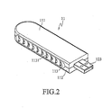
- an electronic device of the invention includes a cabinet 11, a circuit board 12 and a heatsink 13.
- the cabinet 11 is composed of an upper case 111, a lower case 112 and a side panel 113.
- the upper case 111, the lower case 112 and the side panel 113 are assembled to form a containing space.
- Several vents 1131 of via holes are formed on the side panel 113.
- the circuit board 12 has a plurality of electronic components mounted thereon for performing preset functions.
- the circuit board 12 includes at least a processor chip 121.
- the processor chip 121 is a digital video broadcasting (DVB) chip that receives digital video signal through an antenna 122, processes the signal and transfers it to a computer (not shown) via a connector 123 for a user to view the video broadcasting programs through the computer.
- the heatsink 13 is a metal plate with a high thermal conductivity.
- the heatsink 13 can further comprise at least one cutoff 13 according to product requirements.
- the circuit board 12 is installed inside the cabinet 11.
- the heatsink 13 is closely mounted on top of the processor chip 121.
- the cutoff 131 on the heatsink 13 is for some components on the circuit board 12 to pass through.
- a suitable thermal conductive sealant (not shown in the drawing) can be applied between the processor chip 121 and the heatsink 13.
- the connector 123 in the embodiment of the invention is a Universal Serial Bus (USB) interface connector that can provide electric power to the electronic device.
- the processor chip 121 receives digital video signals via the antenna 122 and processes the signals.
- the heat generated during the operation is conducted to the heatsink 13 and dissipated by the air coming through the vents 1131 on the side panel 113 of the cabinet 11.
- the cool air comes through the vents 1131 to the interior of the cabinet 11 cools down the temperature of the processor chip 121 via the heatsink 13. Since the heat of the processor 121 is not directly conducted to the cabinet 11, it prevents the cabinet 11 from high temperature and will not hurt the user.
- the heatsink 13 further comprises a plurality of fins 132 at positions where they won't interfere with the electronic components of the circuit board 12 so as to improve heat dissipation efficiency.
- a second heatsink 14 is further located under the circuit board 12 and relatively to the processor chip 121.
- a thermal conductive element 15 links the first and the second heatsinks 13 and 14 so that heat of the first heatsink 13 is conducted to the second heatsink 14.
- the expanded area of the heatsinks 13 and 14 helps temperature reduction of the processor chip 121.
- the circuit board 12 is a double-face circuit board that the other side of the circuit board includes at least a second processor chip 124 so as to reduce the dimension of the whole circuit board 12.
- the second processor chip 124 is connected with a second heatsink 14 so that the heat generated by the second processor chip 124 and conducted to the second heatsink 14 is dissipated by the air coming via the vents 1131 on the side panel 113 of the case 11.
- the second heatsink 14 helps temperature reduction of the second processor chip 124 and prevents the heat from directly conducting to the lower case 112.
- the circuit board 12 is a double-face circuit board that a processor chip 121 contacted with a first heatsink 13 is mounted on the upper side of the board 12, and a second processor chip 124 contacted with a second heatsink 14 is mounted on the lower side of the board 12.
- a thermal conductive element 15 links the first and the second heatsinks 13 and 14 so that any temperature difference caused by different operation frequencies of the chips 121, 124 is conducted between the first heatsink 13 and the second heatsink 14 so as to improve the whole efficiency of heat dissipation.
Abstract
Description
- The invention generally relates to an electronic device, and in particular relates to heat dissipation means of a small electronic device.
- The unceasing technology developments gradually change people's lives. In accordance to such development tendency, many merchants research and develop kinds of portable electronic devices. For example, as a result of digital television development, watching television is unlimited to a fixed location as long as a digital video receiver is being used. A notebook computer may become a portable television when a user links a digital video receiver to the notebook computer, and uses the digital video receiver to receive signals of television channels.
- At the present market, some digital television boxes can meet the carrying needs for most people. However, designs to be light, thin, short and small are always the goals of research and development in electronic products. The objectives of light, thin, short and small mainly include aspects of electronic design and mechanical design. The development of the present integrated circuit technology is capable of reducing the scales of electric circuits. However, a suitable dissipation mechanism is still strongly needed to dissipate the heat generated by the chips on the Integrate Circuits (ICs) during operation.
- The known digital television box has a larger volume so as to mount a ventilation fan therein to dissipate the heat of the chip. However, when the size of processor chip is reduced without difficulty, a heat dissipating fan is unable to be installed in the small space. Without suitable heat dissipation mechanism, the heat of the chip will accumulate and cause an overheat problem. In conventional heat dissipating method, a metal case is often utilized to improve the heat dissipation. However, since the generated heat is directly transmitted to the metal case of the electronic device, it leads to a safe concern due to the massive heat generated by the ICs of the electronic device. For example, in a television box, the operation temperature of processor chips may reach 80 or 90 centigrade degrees. Thus, a user may get hurt if carelessly touches it. Under the design goals of light, thin, short and small, how to carry out heat dissipation safely and effectively is the key point of miniaturization of electronic products.
- The present electronic products, besides the function demands, are also required to be light, thin, short and small as major goals. In the miniaturized process, the heat dissipation is a major problem. Therefore, the invention provides a high-efficient heat dissipation structure for a small electronic device.
- An electronic device structure according to the invention includes a cabinet, a circuit board, at least a processor chip and a heatsink. The processor chip is mounted on the circuit board. The heatsink is mounted on and contacted with the processor chip. The processor chip, the circuit board and the heatsink are assembled in the cabinet. A side panel with a plurality of vents is mounted on a side of the cabinet. When the processor chip operates, the generated heat is conducted to the heatsink and dissipated via the air coming through the vents of the cabinet. The heat is dispersed outside via the vents and the operating temperature of the processor chip is effectively reduced.
- The electronic device structure according to the invention dissipates the heat of the processor chip during operation and prevents the heat from directly conducting to the cabinet. The heat is dispersed outside via the vents on the cabinet so as to avoid user getting hurt from high temperature surface of the cabinet. It becomes a good solution of dissipation of small electronic device.
- Further scope of applicability of the present invention will become apparent from the detailed description given hereinafter. However, it should be understood that the detailed description and specific examples, while indicating preferred embodiments of the invention, are given by way of illustration only, since various changes and modifications within the spirit and scope of the invention will become apparent to those skilled in the art from this detailed description.
- The present invention will become more fully understood from the detailed description given hereinbelow illustration only, and thus are not limitative of the present invention, and wherein:
- FIG. 1 is an exploded view of a first embodiment of the invention;
- FIG. 2 is a perspective view of a first embodiment of the invention;
- FIG. 3 is a sectional view of a first embodiment of the invention;
- FIG. 4 is a sectional view of a second embodiment of the invention;
- FIG. 5 is a sectional view of a third embodiment of the invention;
- FIG. 6 is a sectional view of a fourth embodiment of the invention; and
- FIG. 7 is a sectional view of a fifth embodiment of the invention.
- The structure of electronic device according to the invention is mainly applicable to small electronic devices. The small electronic devices are small type portable electronic devices, such as digital video broadcasting (DVB) devices, MPEG Layer 3 (MP3) music players and so on. In the following detailed description of preferred embodiments of the invention, digital signal processors are taken as examples.
- As shown in FIGS. 1 and 2, an electronic device of the invention includes a
cabinet 11, acircuit board 12 and aheatsink 13. Thecabinet 11 is composed of anupper case 111, alower case 112 and aside panel 113. Theupper case 111, thelower case 112 and theside panel 113 are assembled to form a containing space.Several vents 1131 of via holes are formed on theside panel 113. - The
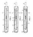
circuit board 12 has a plurality of electronic components mounted thereon for performing preset functions. Thecircuit board 12 includes at least aprocessor chip 121. In this embodiment, theprocessor chip 121 is a digital video broadcasting (DVB) chip that receives digital video signal through anantenna 122, processes the signal and transfers it to a computer (not shown) via aconnector 123 for a user to view the video broadcasting programs through the computer. Theheatsink 13 is a metal plate with a high thermal conductivity. In addition, theheatsink 13 can further comprise at least onecutoff 13 according to product requirements. - Further referring to FIG. 3, a sectional view of the invention, the
circuit board 12 is installed inside thecabinet 11. Theheatsink 13 is closely mounted on top of theprocessor chip 121. Thecutoff 131 on theheatsink 13 is for some components on thecircuit board 12 to pass through. In order to provide good thermal conduction, a suitable thermal conductive sealant (not shown in the drawing) can be applied between theprocessor chip 121 and theheatsink 13. Theconnector 123 in the embodiment of the invention is a Universal Serial Bus (USB) interface connector that can provide electric power to the electronic device. Theprocessor chip 121 receives digital video signals via theantenna 122 and processes the signals. The heat generated during the operation is conducted to theheatsink 13 and dissipated by the air coming through thevents 1131 on theside panel 113 of thecabinet 11. The cool air comes through thevents 1131 to the interior of thecabinet 11 cools down the temperature of theprocessor chip 121 via theheatsink 13. Since the heat of theprocessor 121 is not directly conducted to thecabinet 11, it prevents thecabinet 11 from high temperature and will not hurt the user. - As shown in FIG. 4, a second embodiment of the invention, the
heatsink 13 further comprises a plurality offins 132 at positions where they won't interfere with the electronic components of thecircuit board 12 so as to improve heat dissipation efficiency. - As shown in FIG. 5, a third embodiment of the invention, a
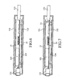
second heatsink 14 is further located under thecircuit board 12 and relatively to theprocessor chip 121. A thermalconductive element 15 links the first and thesecond heatsinks first heatsink 13 is conducted to thesecond heatsink 14. The expanded area of theheatsinks processor chip 121. - As shown in FIG. 6, a fourth embodiment of the invention, the
circuit board 12 is a double-face circuit board that the other side of the circuit board includes at least asecond processor chip 124 so as to reduce the dimension of thewhole circuit board 12. Thesecond processor chip 124 is connected with asecond heatsink 14 so that the heat generated by thesecond processor chip 124 and conducted to thesecond heatsink 14 is dissipated by the air coming via thevents 1131 on theside panel 113 of thecase 11. Thesecond heatsink 14 helps temperature reduction of thesecond processor chip 124 and prevents the heat from directly conducting to thelower case 112. - As shown in FIG. 7, a fifth embodiment of the invention, the
circuit board 12 is a double-face circuit board that aprocessor chip 121 contacted with afirst heatsink 13 is mounted on the upper side of theboard 12, and asecond processor chip 124 contacted with asecond heatsink 14 is mounted on the lower side of theboard 12. A thermalconductive element 15 links the first and thesecond heatsinks chips first heatsink 13 and thesecond heatsink 14 so as to improve the whole efficiency of heat dissipation. - The invention being thus described, it will be obvious that the same may be varied in many ways. Such variations are not to be regarded as a departure from the spirit and scope of the invention, and all such modifications as would be obvious to one skilled in the art are intended to be included within the scope of the following claims.
Claims (7)
- A small electronic device, comprising:a cabinet formed with a plurality of vents;a circuit board, installed inside said cabinet, comprising at least a processor chip and a plurality of electronic components for achieving preset functions; anda first heatsink, installed inside said cabinet, contacted with said processor chip for dissipating the heat generated by said processor chip through said vents.
- The small electronic device according to claim 1 wherein said cabinet comprises an upper case, a lower case and a side panel.
- The small electronic device according to claim 1 wherein said first heatsink comprises a plurality of fms.
- The small electronic device according to claim 1 wherein said first heatsink is formed with at least a cutoff.
- The small electronic device according to claim 1 further comprising a second processor chip mounted on bottom side of said circuit board, and a second heatsink contacted to said second processor chip for dissipating the heat of said second processor chip.
- The small electronic device according to claim 5 further comprising a thermal conductive element disposed between said first heatsink and said second heatsink.
- The small electronic device according to claim 1 further comprising a second heatsink located under said circuit board; and a thermal conductive element disposed between said first heatsink and said second heatsink.
Priority Applications (3)
| Application Number | Priority Date | Filing Date | Title |
|---|---|---|---|
| EP05024631A EP1785807B1 (en) | 2005-11-11 | 2005-11-11 | Cooling of a small electronic device with a USB connector |
| AT05024631T ATE426197T1 (en) | 2005-11-11 | 2005-11-11 | COOLING A SMALL ELECTRONIC DEVICE WITH A USB CONNECTOR. |
| DE602005013394T DE602005013394D1 (en) | 2005-11-11 | 2005-11-11 | Cooling of a small electronic device with a USB connector. |
Applications Claiming Priority (1)
| Application Number | Priority Date | Filing Date | Title |
|---|---|---|---|
| EP05024631A EP1785807B1 (en) | 2005-11-11 | 2005-11-11 | Cooling of a small electronic device with a USB connector |
Publications (2)
| Publication Number | Publication Date |
|---|---|
| EP1785807A1 true EP1785807A1 (en) | 2007-05-16 |
| EP1785807B1 EP1785807B1 (en) | 2009-03-18 |
Family
ID=35717727
Family Applications (1)
| Application Number | Title | Priority Date | Filing Date |
|---|---|---|---|
| EP05024631A Not-in-force EP1785807B1 (en) | 2005-11-11 | 2005-11-11 | Cooling of a small electronic device with a USB connector |
Country Status (3)
| Country | Link |
|---|---|
| EP (1) | EP1785807B1 (en) |
| AT (1) | ATE426197T1 (en) |
| DE (1) | DE602005013394D1 (en) |
Cited By (3)
| Publication number | Priority date | Publication date | Assignee | Title |
|---|---|---|---|---|
| EP2315511A1 (en) | 2009-10-23 | 2011-04-27 | Walton Advanced Engineering Inc. | Heat dissipation device of electronic circuit modules |
| CN103715543A (en) * | 2012-09-28 | 2014-04-09 | 启碁科技股份有限公司 | Electronic device and plug and play unit thereof |
| EP2819021A4 (en) * | 2012-04-16 | 2015-05-06 | Zte Corp | Wireless communication terminal |
Citations (5)
| Publication number | Priority date | Publication date | Assignee | Title |
|---|---|---|---|---|
| US5659459A (en) * | 1992-05-20 | 1997-08-19 | Seiko Epson Corporation | Cartridge for electronic devices including grounding pads and conductive shielding to decrease the wavelength of emitted electromagnetic radiation |
| US20040008502A1 (en) * | 2000-07-19 | 2004-01-15 | Frederic Hautier | Pack provided with an antenna extension for electronic card and method for the assembling of the pack |
| US6781846B1 (en) * | 1996-01-17 | 2004-08-24 | Fujitsu Limited | IC card and IC card cooling tray |
| US20050024526A1 (en) * | 2003-07-28 | 2005-02-03 | Mu-Jung Wang | Multi-function portable disk |
| US20050088827A1 (en) * | 2003-10-07 | 2005-04-28 | Min Zhang | Electrical card having heatsink device |
-
2005
- 2005-11-11 DE DE602005013394T patent/DE602005013394D1/en active Active
- 2005-11-11 AT AT05024631T patent/ATE426197T1/en not_active IP Right Cessation
- 2005-11-11 EP EP05024631A patent/EP1785807B1/en not_active Not-in-force
Patent Citations (5)
| Publication number | Priority date | Publication date | Assignee | Title |
|---|---|---|---|---|
| US5659459A (en) * | 1992-05-20 | 1997-08-19 | Seiko Epson Corporation | Cartridge for electronic devices including grounding pads and conductive shielding to decrease the wavelength of emitted electromagnetic radiation |
| US6781846B1 (en) * | 1996-01-17 | 2004-08-24 | Fujitsu Limited | IC card and IC card cooling tray |
| US20040008502A1 (en) * | 2000-07-19 | 2004-01-15 | Frederic Hautier | Pack provided with an antenna extension for electronic card and method for the assembling of the pack |
| US20050024526A1 (en) * | 2003-07-28 | 2005-02-03 | Mu-Jung Wang | Multi-function portable disk |
| US20050088827A1 (en) * | 2003-10-07 | 2005-04-28 | Min Zhang | Electrical card having heatsink device |
Cited By (3)
| Publication number | Priority date | Publication date | Assignee | Title |
|---|---|---|---|---|
| EP2315511A1 (en) | 2009-10-23 | 2011-04-27 | Walton Advanced Engineering Inc. | Heat dissipation device of electronic circuit modules |
| EP2819021A4 (en) * | 2012-04-16 | 2015-05-06 | Zte Corp | Wireless communication terminal |
| CN103715543A (en) * | 2012-09-28 | 2014-04-09 | 启碁科技股份有限公司 | Electronic device and plug and play unit thereof |
Also Published As
| Publication number | Publication date |
|---|---|
| DE602005013394D1 (en) | 2009-04-30 |
| ATE426197T1 (en) | 2009-04-15 |
| EP1785807B1 (en) | 2009-03-18 |
Similar Documents
| Publication | Publication Date | Title |
|---|---|---|
| US5430609A (en) | Microprocessor cooling in a portable computer | |
| US6577504B1 (en) | Integrated heat sink for different size components with EMI suppression features | |
| US8059401B2 (en) | Electronic device with heat dissipation module | |
| US7990720B2 (en) | Electronic system with heat dissipation structure | |
| US8757963B2 (en) | Thermal module with airflow guiding function | |
| US20050286229A1 (en) | Modular heat-dissipation assembly structure for a PCB | |
| US20080007914A1 (en) | Heat dissipation device | |
| JP2006269639A (en) | Heat radiating device and on-vehicle electronic equipment | |
| US20080130234A1 (en) | Electronic Apparatus | |
| JP2011081437A (en) | Electronic equipment | |
| US9357676B2 (en) | Cooling device and electronic apparatus | |
| US7929302B2 (en) | Cooling device | |
| US6768633B2 (en) | External power supply module adapted to be disposed in a portable electronic apparatus | |
| US20080068797A1 (en) | Mounting assembly and electronic device with the mounting assembly | |
| US7859843B2 (en) | Heat dissipation structure | |
| JP2008198864A (en) | Electronic equipment and semiconductor package | |
| US20210068311A1 (en) | Host computer and computer system for vehicle | |
| US20120069522A1 (en) | Thermal module and electronic device incorporating the same | |
| KR101672738B1 (en) | electronic device having cooling structure | |
| US6781832B2 (en) | Cooling unit for cooling heat generating component and electronic apparatus containing cooling unit | |
| US7254029B2 (en) | Printed circuit board with a heat dissipation device | |
| EP1785807A1 (en) | Cooling of a small electronic device with a USB connector | |
| US9310858B2 (en) | Heat dissipating module with enhanced heat dissipation efficiency and electronic device therewith | |
| JP2001318738A (en) | Electronic equipment | |
| JPH05298961A (en) | Portable electronic computer |
Legal Events
| Date | Code | Title | Description |
|---|---|---|---|
| PUAI | Public reference made under article 153(3) epc to a published international application that has entered the european phase |
Free format text: ORIGINAL CODE: 0009012 |
|
| AK | Designated contracting states |
Kind code of ref document: A1 Designated state(s): AT BE BG CH CY CZ DE DK EE ES FI FR GB GR HU IE IS IT LI LT LU LV MC NL PL PT RO SE SI SK TR |
|
| AX | Request for extension of the european patent |
Extension state: AL BA HR MK YU |
|
| 17P | Request for examination filed |
Effective date: 20070626 |
|
| AKX | Designation fees paid |
Designated state(s): AT BE BG CH CY CZ DE DK EE ES FI FR GB GR HU IE IS IT LI LT LU LV MC NL PL PT RO SE SI SK TR |
|
| GRAP | Despatch of communication of intention to grant a patent |
Free format text: ORIGINAL CODE: EPIDOSNIGR1 |
|
| GRAS | Grant fee paid |
Free format text: ORIGINAL CODE: EPIDOSNIGR3 |
|
| GRAA | (expected) grant |
Free format text: ORIGINAL CODE: 0009210 |
|
| AK | Designated contracting states |
Kind code of ref document: B1 Designated state(s): AT BE BG CH CY CZ DE DK EE ES FI FR GB GR HU IE IS IT LI LT LU LV MC NL PL PT RO SE SI SK TR |
|
| REG | Reference to a national code |
Ref country code: GB Ref legal event code: FG4D |
|
| REG | Reference to a national code |
Ref country code: CH Ref legal event code: EP |
|
| REG | Reference to a national code |
Ref country code: IE Ref legal event code: FG4D |
|
| REF | Corresponds to: |
Ref document number: 602005013394 Country of ref document: DE Date of ref document: 20090430 Kind code of ref document: P |
|
| PG25 | Lapsed in a contracting state [announced via postgrant information from national office to epo] |
Ref country code: FI Free format text: LAPSE BECAUSE OF FAILURE TO SUBMIT A TRANSLATION OF THE DESCRIPTION OR TO PAY THE FEE WITHIN THE PRESCRIBED TIME-LIMIT Effective date: 20090318 Ref country code: SI Free format text: LAPSE BECAUSE OF FAILURE TO SUBMIT A TRANSLATION OF THE DESCRIPTION OR TO PAY THE FEE WITHIN THE PRESCRIBED TIME-LIMIT Effective date: 20090318 Ref country code: LT Free format text: LAPSE BECAUSE OF FAILURE TO SUBMIT A TRANSLATION OF THE DESCRIPTION OR TO PAY THE FEE WITHIN THE PRESCRIBED TIME-LIMIT Effective date: 20090318 Ref country code: NL Free format text: LAPSE BECAUSE OF FAILURE TO SUBMIT A TRANSLATION OF THE DESCRIPTION OR TO PAY THE FEE WITHIN THE PRESCRIBED TIME-LIMIT Effective date: 20090318 |
|
| PG25 | Lapsed in a contracting state [announced via postgrant information from national office to epo] |
Ref country code: AT Free format text: LAPSE BECAUSE OF FAILURE TO SUBMIT A TRANSLATION OF THE DESCRIPTION OR TO PAY THE FEE WITHIN THE PRESCRIBED TIME-LIMIT Effective date: 20090318 Ref country code: SE Free format text: LAPSE BECAUSE OF FAILURE TO SUBMIT A TRANSLATION OF THE DESCRIPTION OR TO PAY THE FEE WITHIN THE PRESCRIBED TIME-LIMIT Effective date: 20090618 Ref country code: LV Free format text: LAPSE BECAUSE OF FAILURE TO SUBMIT A TRANSLATION OF THE DESCRIPTION OR TO PAY THE FEE WITHIN THE PRESCRIBED TIME-LIMIT Effective date: 20090318 Ref country code: PL Free format text: LAPSE BECAUSE OF FAILURE TO SUBMIT A TRANSLATION OF THE DESCRIPTION OR TO PAY THE FEE WITHIN THE PRESCRIBED TIME-LIMIT Effective date: 20090318 |
|
| NLV1 | Nl: lapsed or annulled due to failure to fulfill the requirements of art. 29p and 29m of the patents act | ||
| PG25 | Lapsed in a contracting state [announced via postgrant information from national office to epo] |
Ref country code: BE Free format text: LAPSE BECAUSE OF FAILURE TO SUBMIT A TRANSLATION OF THE DESCRIPTION OR TO PAY THE FEE WITHIN THE PRESCRIBED TIME-LIMIT Effective date: 20090318 |
|
| PG25 | Lapsed in a contracting state [announced via postgrant information from national office to epo] |
Ref country code: PT Free format text: LAPSE BECAUSE OF FAILURE TO SUBMIT A TRANSLATION OF THE DESCRIPTION OR TO PAY THE FEE WITHIN THE PRESCRIBED TIME-LIMIT Effective date: 20090826 Ref country code: ES Free format text: LAPSE BECAUSE OF FAILURE TO SUBMIT A TRANSLATION OF THE DESCRIPTION OR TO PAY THE FEE WITHIN THE PRESCRIBED TIME-LIMIT Effective date: 20090629 Ref country code: EE Free format text: LAPSE BECAUSE OF FAILURE TO SUBMIT A TRANSLATION OF THE DESCRIPTION OR TO PAY THE FEE WITHIN THE PRESCRIBED TIME-LIMIT Effective date: 20090318 Ref country code: CZ Free format text: LAPSE BECAUSE OF FAILURE TO SUBMIT A TRANSLATION OF THE DESCRIPTION OR TO PAY THE FEE WITHIN THE PRESCRIBED TIME-LIMIT Effective date: 20090318 |
|
| PG25 | Lapsed in a contracting state [announced via postgrant information from national office to epo] |
Ref country code: SK Free format text: LAPSE BECAUSE OF FAILURE TO SUBMIT A TRANSLATION OF THE DESCRIPTION OR TO PAY THE FEE WITHIN THE PRESCRIBED TIME-LIMIT Effective date: 20090318 Ref country code: RO Free format text: LAPSE BECAUSE OF FAILURE TO SUBMIT A TRANSLATION OF THE DESCRIPTION OR TO PAY THE FEE WITHIN THE PRESCRIBED TIME-LIMIT Effective date: 20090318 Ref country code: IS Free format text: LAPSE BECAUSE OF FAILURE TO SUBMIT A TRANSLATION OF THE DESCRIPTION OR TO PAY THE FEE WITHIN THE PRESCRIBED TIME-LIMIT Effective date: 20090718 |
|
| PLBE | No opposition filed within time limit |
Free format text: ORIGINAL CODE: 0009261 |
|
| STAA | Information on the status of an ep patent application or granted ep patent |
Free format text: STATUS: NO OPPOSITION FILED WITHIN TIME LIMIT |
|
| PG25 | Lapsed in a contracting state [announced via postgrant information from national office to epo] |
Ref country code: BG Free format text: LAPSE BECAUSE OF FAILURE TO SUBMIT A TRANSLATION OF THE DESCRIPTION OR TO PAY THE FEE WITHIN THE PRESCRIBED TIME-LIMIT Effective date: 20090618 Ref country code: DK Free format text: LAPSE BECAUSE OF FAILURE TO SUBMIT A TRANSLATION OF THE DESCRIPTION OR TO PAY THE FEE WITHIN THE PRESCRIBED TIME-LIMIT Effective date: 20090318 |
|
| 26N | No opposition filed |
Effective date: 20091221 |
|
| PG25 | Lapsed in a contracting state [announced via postgrant information from national office to epo] |
Ref country code: MC Free format text: LAPSE BECAUSE OF NON-PAYMENT OF DUE FEES Effective date: 20091130 |
|
| REG | Reference to a national code |
Ref country code: CH Ref legal event code: PL |
|
| PG25 | Lapsed in a contracting state [announced via postgrant information from national office to epo] |
Ref country code: CH Free format text: LAPSE BECAUSE OF NON-PAYMENT OF DUE FEES Effective date: 20091130 Ref country code: LI Free format text: LAPSE BECAUSE OF NON-PAYMENT OF DUE FEES Effective date: 20091130 Ref country code: IE Free format text: LAPSE BECAUSE OF NON-PAYMENT OF DUE FEES Effective date: 20091111 Ref country code: GR Free format text: LAPSE BECAUSE OF FAILURE TO SUBMIT A TRANSLATION OF THE DESCRIPTION OR TO PAY THE FEE WITHIN THE PRESCRIBED TIME-LIMIT Effective date: 20090619 |
|
| PGFP | Annual fee paid to national office [announced via postgrant information from national office to epo] |
Ref country code: FR Payment date: 20101214 Year of fee payment: 6 |
|
| PG25 | Lapsed in a contracting state [announced via postgrant information from national office to epo] |
Ref country code: IT Free format text: LAPSE BECAUSE OF FAILURE TO SUBMIT A TRANSLATION OF THE DESCRIPTION OR TO PAY THE FEE WITHIN THE PRESCRIBED TIME-LIMIT Effective date: 20090318 |
|
| PGFP | Annual fee paid to national office [announced via postgrant information from national office to epo] |
Ref country code: GB Payment date: 20101019 Year of fee payment: 6 |
|
| PG25 | Lapsed in a contracting state [announced via postgrant information from national office to epo] |
Ref country code: LU Free format text: LAPSE BECAUSE OF NON-PAYMENT OF DUE FEES Effective date: 20091111 |
|
| PGFP | Annual fee paid to national office [announced via postgrant information from national office to epo] |
Ref country code: DE Payment date: 20110131 Year of fee payment: 6 |
|
| PG25 | Lapsed in a contracting state [announced via postgrant information from national office to epo] |
Ref country code: HU Free format text: LAPSE BECAUSE OF FAILURE TO SUBMIT A TRANSLATION OF THE DESCRIPTION OR TO PAY THE FEE WITHIN THE PRESCRIBED TIME-LIMIT Effective date: 20090919 |
|
| PG25 | Lapsed in a contracting state [announced via postgrant information from national office to epo] |
Ref country code: TR Free format text: LAPSE BECAUSE OF FAILURE TO SUBMIT A TRANSLATION OF THE DESCRIPTION OR TO PAY THE FEE WITHIN THE PRESCRIBED TIME-LIMIT Effective date: 20090318 |
|
| PG25 | Lapsed in a contracting state [announced via postgrant information from national office to epo] |
Ref country code: CY Free format text: LAPSE BECAUSE OF FAILURE TO SUBMIT A TRANSLATION OF THE DESCRIPTION OR TO PAY THE FEE WITHIN THE PRESCRIBED TIME-LIMIT Effective date: 20090318 |
|
| GBPC | Gb: european patent ceased through non-payment of renewal fee |
Effective date: 20111111 |
|
| REG | Reference to a national code |
Ref country code: FR Ref legal event code: ST Effective date: 20120731 |
|
| REG | Reference to a national code |
Ref country code: DE Ref legal event code: R119 Ref document number: 602005013394 Country of ref document: DE Effective date: 20120601 |
|
| PG25 | Lapsed in a contracting state [announced via postgrant information from national office to epo] |
Ref country code: GB Free format text: LAPSE BECAUSE OF NON-PAYMENT OF DUE FEES Effective date: 20111111 |
|
| PG25 | Lapsed in a contracting state [announced via postgrant information from national office to epo] |
Ref country code: FR Free format text: LAPSE BECAUSE OF NON-PAYMENT OF DUE FEES Effective date: 20111130 |
|
| PG25 | Lapsed in a contracting state [announced via postgrant information from national office to epo] |
Ref country code: DE Free format text: LAPSE BECAUSE OF NON-PAYMENT OF DUE FEES Effective date: 20120601 |