EP1784057A1 - Red phosphorescent compounds and organic electroluminescent devices using the same - Google Patents
Red phosphorescent compounds and organic electroluminescent devices using the same Download PDFInfo
- Publication number
- EP1784057A1 EP1784057A1 EP06023132A EP06023132A EP1784057A1 EP 1784057 A1 EP1784057 A1 EP 1784057A1 EP 06023132 A EP06023132 A EP 06023132A EP 06023132 A EP06023132 A EP 06023132A EP 1784057 A1 EP1784057 A1 EP 1784057A1
- Authority
- EP
- European Patent Office
- Prior art keywords
- pentanedione
- organic
- red phosphorescent
- light
- luminance
- Prior art date
- Legal status (The legal status is an assumption and is not a legal conclusion. Google has not performed a legal analysis and makes no representation as to the accuracy of the status listed.)
- Granted
Links
- 0 Cc(c1c2cccc1)c*(C)c2-c1c(C)c(*)c(*)c(O*)c1C Chemical compound Cc(c1c2cccc1)c*(C)c2-c1c(C)c(*)c(*)c(O*)c1C 0.000 description 5
- VDFVNEFVBPFDSB-UHFFFAOYSA-N C1COCOC1 Chemical compound C1COCOC1 VDFVNEFVBPFDSB-UHFFFAOYSA-N 0.000 description 2
- CFZVTEUJJFFUBX-UHFFFAOYSA-N NC(C(CC(C(N)(N)I)=O)=O)(N)I Chemical compound NC(C(CC(C(N)(N)I)=O)=O)(N)I CFZVTEUJJFFUBX-UHFFFAOYSA-N 0.000 description 1
Images


Classifications
-
- C—CHEMISTRY; METALLURGY
- C07—ORGANIC CHEMISTRY
- C07F—ACYCLIC, CARBOCYCLIC OR HETEROCYCLIC COMPOUNDS CONTAINING ELEMENTS OTHER THAN CARBON, HYDROGEN, HALOGEN, OXYGEN, NITROGEN, SULFUR, SELENIUM OR TELLURIUM
- C07F15/00—Compounds containing elements of Groups 8, 9, 10 or 18 of the Periodic Table
- C07F15/0006—Compounds containing elements of Groups 8, 9, 10 or 18 of the Periodic Table compounds of the platinum group
- C07F15/0033—Iridium compounds
-
- C—CHEMISTRY; METALLURGY
- C09—DYES; PAINTS; POLISHES; NATURAL RESINS; ADHESIVES; COMPOSITIONS NOT OTHERWISE PROVIDED FOR; APPLICATIONS OF MATERIALS NOT OTHERWISE PROVIDED FOR
- C09K—MATERIALS FOR MISCELLANEOUS APPLICATIONS, NOT PROVIDED FOR ELSEWHERE
- C09K11/00—Luminescent materials, e.g. electroluminescent or chemiluminescent
- C09K11/06—Luminescent materials, e.g. electroluminescent or chemiluminescent containing organic luminescent materials
-
- H—ELECTRICITY
- H05—ELECTRIC TECHNIQUES NOT OTHERWISE PROVIDED FOR
- H05B—ELECTRIC HEATING; ELECTRIC LIGHT SOURCES NOT OTHERWISE PROVIDED FOR; CIRCUIT ARRANGEMENTS FOR ELECTRIC LIGHT SOURCES, IN GENERAL
- H05B33/00—Electroluminescent light sources
- H05B33/12—Light sources with substantially two-dimensional [2D] radiating surfaces
- H05B33/14—Light sources with substantially two-dimensional [2D] radiating surfaces characterised by the chemical or physical composition or the arrangement of the electroluminescent material, or by the simultaneous addition of the electroluminescent material in or onto the light source
-
- C—CHEMISTRY; METALLURGY
- C09—DYES; PAINTS; POLISHES; NATURAL RESINS; ADHESIVES; COMPOSITIONS NOT OTHERWISE PROVIDED FOR; APPLICATIONS OF MATERIALS NOT OTHERWISE PROVIDED FOR
- C09K—MATERIALS FOR MISCELLANEOUS APPLICATIONS, NOT PROVIDED FOR ELSEWHERE
- C09K2211/00—Chemical nature of organic luminescent or tenebrescent compounds
- C09K2211/10—Non-macromolecular compounds
- C09K2211/1003—Carbocyclic compounds
- C09K2211/1007—Non-condensed systems
-
- C—CHEMISTRY; METALLURGY
- C09—DYES; PAINTS; POLISHES; NATURAL RESINS; ADHESIVES; COMPOSITIONS NOT OTHERWISE PROVIDED FOR; APPLICATIONS OF MATERIALS NOT OTHERWISE PROVIDED FOR
- C09K—MATERIALS FOR MISCELLANEOUS APPLICATIONS, NOT PROVIDED FOR ELSEWHERE
- C09K2211/00—Chemical nature of organic luminescent or tenebrescent compounds
- C09K2211/10—Non-macromolecular compounds
- C09K2211/1018—Heterocyclic compounds
- C09K2211/1025—Heterocyclic compounds characterised by ligands
- C09K2211/1029—Heterocyclic compounds characterised by ligands containing one nitrogen atom as the heteroatom
-
- C—CHEMISTRY; METALLURGY
- C09—DYES; PAINTS; POLISHES; NATURAL RESINS; ADHESIVES; COMPOSITIONS NOT OTHERWISE PROVIDED FOR; APPLICATIONS OF MATERIALS NOT OTHERWISE PROVIDED FOR
- C09K—MATERIALS FOR MISCELLANEOUS APPLICATIONS, NOT PROVIDED FOR ELSEWHERE
- C09K2211/00—Chemical nature of organic luminescent or tenebrescent compounds
- C09K2211/18—Metal complexes
- C09K2211/185—Metal complexes of the platinum group, i.e. Os, Ir, Pt, Ru, Rh or Pd
-
- C—CHEMISTRY; METALLURGY
- C09—DYES; PAINTS; POLISHES; NATURAL RESINS; ADHESIVES; COMPOSITIONS NOT OTHERWISE PROVIDED FOR; APPLICATIONS OF MATERIALS NOT OTHERWISE PROVIDED FOR
- C09K—MATERIALS FOR MISCELLANEOUS APPLICATIONS, NOT PROVIDED FOR ELSEWHERE
- C09K2211/00—Chemical nature of organic luminescent or tenebrescent compounds
- C09K2211/18—Metal complexes
- C09K2211/186—Metal complexes of the light metals other than alkali metals and alkaline earth metals, i.e. Be, Al or Mg
-
- C—CHEMISTRY; METALLURGY
- C09—DYES; PAINTS; POLISHES; NATURAL RESINS; ADHESIVES; COMPOSITIONS NOT OTHERWISE PROVIDED FOR; APPLICATIONS OF MATERIALS NOT OTHERWISE PROVIDED FOR
- C09K—MATERIALS FOR MISCELLANEOUS APPLICATIONS, NOT PROVIDED FOR ELSEWHERE
- C09K2211/00—Chemical nature of organic luminescent or tenebrescent compounds
- C09K2211/18—Metal complexes
- C09K2211/188—Metal complexes of other metals not provided for in one of the previous groups
Definitions
- the present invention relates to red light-emitting phosphorescent compounds (hereinafter, referred to simply to as 'red phosphorescent compounds') and organic electroluminescent (EL) devices using the same. More particularly, the present invention relates to red phosphorescent compounds, and organic electroluminescent devices comprising a laminate of an anode, a light-emitting layer and a cathode wherein one of the red phosphorescent compounds is used as a dopant of the light-emitting layer.
- red phosphorescent compounds hereinafter, referred to simply to as 'red phosphorescent compounds'
- EL organic electroluminescent
- Organic electroluminescent devices When charge carriers are injected into an organic film formed between an electron injecting electrode (cathode) and a hole injecting electrode (anode) of an organic electroluminescent device, electrons combine with holes to create electron-hole pairs, which then decay to emit light.
- Organic electroluminescent devices have advantages in that they can be fabricated on flexible transparent substrates (e.g. , plastic substrates) and can be operated at a voltage ( e.g. , 10V or below) lower than voltages required to operate plasma display panels (PDPs) and inorganic electroluminescent devices. Other advantages of organic electroluminescent devices are relatively low power consumption and excellent color representation.
- organic electroluminescent (EL) devices can emit light of three colors (i.e., green, blue and red), they have been the focus of intense interest lately as next-generation display devices capable of producing images of various colors.
- a general method for fabricating organic EL devices will be briefly explained below.
- ITO Indium tin oxide
- a hole injecting layer is formed to a thickness of 10 to 30 nm on the anode.
- Copper (II) phthalocyanine (CuPc) is mainly used as a material of the hole injecting layer.
- a hole transport layer is introduced into the resulting structure.
- the hole transport layer is formed by depositing 4,4'-bis[N-(1-naphthyl)-N-phenylamino]-biphenyl (NPB) to a thickness of about 30 to about 60 nm on the hole injecting layer.
- An organic light-emitting layer is formed on the hole transport layer. If necessary, a dopant may be added to a material for the organic light-emitting layer.
- a dopant may be added to a material for the organic light-emitting layer.
- tris(8-hydroxyquinoline)aluminum (Alq 3 ) as a material for the organic light-emitting layer is deposited to a thickness of about 30 to about 60 nm on the hole transport layer, and N-methylquinacridone (MQD) is mainly used as the dopant.
- An electron transport layer (ETL) and an electron injecting layer (EIL) are sequentially formed on the organic light-emitting layer.
- an electron injecting/transport layer is formed on the organic light-emitting layer.
- the formation of the electron injecting/transport layer may be unnecessary.
- a cathode material is coated on the electron injecting layer, and finally a passivation film is covered thereon.
- the type of the organic electroluminescent devices i.e. blue, green and red light-emitting devices
- the type of the organic electroluminescent devices i.e. blue, green and red light-emitting devices
- Phosphorescent materials for use in organic EL devices must satisfy the requirements of high luminescence efficiency, high color purity and long luminescence lifetime. As shown in FIG. 1, as the color purity of an organic EL device using a red phosphorescent material becomes higher (i.e . as the x-values on CIE chromaticity coordinates increase), the spectral luminous efficacy of the organic EL device decreases, making it difficult to achieve high luminescence efficiency of the organic EL device.
- the present invention is directed to red phosphorescent compounds and organic electroluminescent (EL) devices using the same that substantially obviate one or more problems due to limitations and disadvantages of the related art.
- An object of the present invention is to provide compounds of Formulas 1 to 3 that follow.
- Another object of the present invention is to provide organic electroluminescent (EL) devices with high color purity, high luminance and long lifetime which use one of the compounds as a dopant of a light-emitting layer.
- EL organic electroluminescent
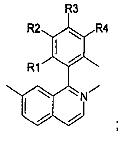
- R1 and R2 are independently a C 1 -C 4 alkyl group
- R3, R4, R5 and R6 are independently selected from hydrogen, C 1 -C 4 alkyl groups and C 1 -C 4 alkoxy groups
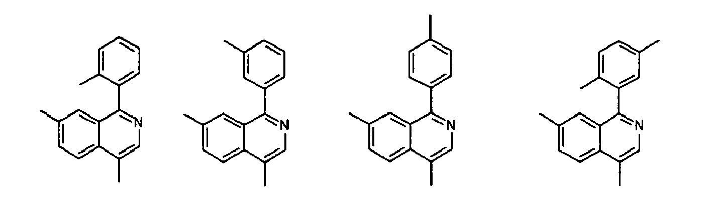
- Examples of preferred compounds that can be represented by Formula 1 include the following compounds:
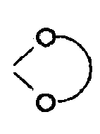
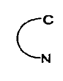
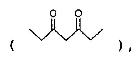
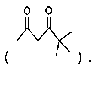
- R1, R2, R3 and R4 are independently selected from C 1 -C 4 alkyl groups and C 1 -C 4 alkoxy groups; and is selected from 2,4-pentanedione, 2,2,6,6,-tetramethylheptane-3,5-dione, 1,3-propanedione, 1,3-butanedione, 3,5-heptanedione, 1,1,1-trifluoro-2,4-pentanedione, 1,1,1,5,5,5-hexafluoro-2,4-pentanedione and 2,2-dimethyl-3,5-hexanedione.
- Examples of preferred compounds that can be represented by Formula 2 include the following compounds:
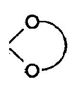
- R1, R2, R3 and R4 are independently selected from hydrogen, C 1 -C 4 alkyl groups and C 1 -C 4 alkoxy groups; and is selected from 2,4-pentanedione, 2,2,6,6,-tetramethylheptane-3,5-dione, 1,3-propanedione, 1,3-butanedione, 3,5-heptanedione, 1,1,1-trifluoro-2,4-pentanedione, 1,1,1,5,5,5-hexafluoro-2,4-pentanedione and 2,2-dimethyl-3,5-hexanedione.
- Examples of preferred compounds that can be represented by Formula 3 include the following compounds:
- an organic electroluminescent (EL) device comprising an anode, a hole injecting layer (HIL), a hole transport layer (HTL), an light-emitting layer, an electron transport layer (ETL) and an electron injecting layer (EIL), and a cathode laminated in this order wherein one of the red phosphorescent compounds of Formulas 1 to 3 is used as a dopant of the light-emitting layer.
- HIL hole injecting layer
- HTL hole transport layer
- ETL electron transport layer
- EIL electron injecting layer
- a host used in the organic light-emitting layer of the organic EL device according to the present invention may be selected from Al complexes, Zn complexes, and carbazole derivatives.
- the dopant may be preferably used in an amount of 0.5 to 20% by weight, based on the weight of the host. When the dopant is used within this range, the desired effects of the organic EL device can be achieved.
- the Al and Zn complexes may have at least one ligand selected from quinolyl, biphenyl, isoquinolyl, phenyl, naphthyl, methylquinolyl, dimethylquinolyl and dimethylisoquinolyl groups.
- the carbazole derivatives may be preferably 4,4'-N,N' dicarbazole biphenyl (CBP).
- FIG. 1 shows a graph showing a phenomenon wherein the color purity of an organic EL device becomes higher (i.e. as the x-values on CIE chromaticity coordinates increase), the relative sensitivity of the organic EL device decreases;
- FIG. 2 shows the structural formulas of NPB, copper (II) phthalocyanine (CuPc), (btp) 2 Ir(acac), Alq 3 , BAlq and CBP used in Example Section according to the present invention.
- N-(2-hydroxy-1-p-tolyl-propyl)-3-methylbezamide (2.1 mmol), phosphorus (V) oxide (10 mmol) and decahydronaphtalene (50 mmol) were put in a dried two-neck round-bottom flask. Then, the mixture was stirred at 120 ⁇ for 5 hours. After completion of the reaction, the reaction mixture was extracted with dichloromethane and water and distilled under reduced pressure. The resulting residue was purified by silica gel column chromatography. The eluate was distilled under reduced pressure. The residue was recrystallized from dichloromethane and petroleum ether, and filtered to yield 1-(3-methylphenyl)-4,7-dimethylisoquinoline.
- the dichloro-crosslinked dimer complex (1 mmol), 2,4-pentanedione (3 mmol), sodium carbonate (Na 2 CO 3 ) (6 mmol) and 2-ethoxyethanol (30 mL) were put in a dried two-neck round-bottom flask. Then, the mixture was refluxed for 2 hours. The reaction mixture was allowed to cool to room temperature, and then distilled water was added thereto to obtain a solid. The solid was filtered and dissolved in dichloromethane. The solution was filtered through silica gel.
- the dichloro-crosslinked dimer complex (1 mmol), 2,4-pentanedione (3 mmol), sodium carbonate (Na 2 CO 3 ) (6 mmol) and 2-ethoxyethanol (30 mL) were put in a dried two-neck round-bottom flask. Then, the mixture was refluxed for 24 hours. The reaction mixture was allowed to cool to room temperature, and then distilled water was added thereto to obtain a solid. The solid was filtered and dissolved in dichloromethane. The solution was filtered through silica gel.
- the dichloro-crosslinked dimer complex (1 mmol), 2,4-pentanedione (3 mmol), sodium carbonate (Na 2 CO 3 ) (6 mmol) and 2-ethoxyethanol (30 mL) were put in a dried two-neck round-bottom flask. Then, the mixture was stirred for 24 hours. After the mixture was allowed to cool to room temperature, distilled water was added thereto to obtain a solid. The solid was filtered and dissolved in dichloromethane. The solution was filtered through silica gel.
- An ITO-coated glass substrate was patterned to have a light-emitting area of 3 mm x 3 mm, followed by cleaning. After the patterned substrate was disposed in a vacuum chamber, the standard pressure of the chamber was adjusted to 1 x 10 -6 torr. CuPc (200 ⁇ ), NPD (400 ⁇ ), BAlq + A-1 (7%) (200 ⁇ ), Alq 3 (300 ⁇ ), LiF (5 ⁇ ) and Al (1000 ⁇ ) were sequentially deposited on the ITO glass substrate to fabricate an organic EL device.
- the lifetime (defined as the time taken before the luminance of the organic EL device decreases to half its initial value) of the organic EL device was 5,100 hours at 2,000 cd/m 2 .
- An ITO-coated glass substrate was patterned to have a light-emitting area of 3 mm x 3 mm, followed by cleaning. After the patterned substrate was disposed in a vacuum chamber, the standard pressure of the chamber was adjusted to 1x10 -6 torr. CuPc (200 ⁇ ), NPD (400 ⁇ ), BAlq + A-2 (7%) (200 ⁇ ), Alq 3 (300 ⁇ ), LiF (5 ⁇ ) and Al (1000 ⁇ ) were sequentially deposited on the ITO glass substrate to fabricate an organic EL device.
- the lifetime (defined as the time taken before the luminance of the organic EL device decreases to half its initial value) of the organic EL device was 4,800 hours at 2,000 cd/m 2 .
- An ITO-coated glass substrate was patterned to have a light-emitting area of 3 mm x 3 mm, followed by cleaning. After the patterned substrate was disposed in a vacuum chamber, the standard pressure of the chamber was adjusted to 1 x 10 -6 torr. CuPc (200 ⁇ ), NPD (400 ⁇ ), BAlq + A-7 (7%) (200 ⁇ ), Alq 3 (300 ⁇ ), LiF (5 ⁇ ) and A1 (1000 ⁇ ) were sequentially deposited on the ITO glass substrate to fabricate an organic EL device.
- the luminance of the organic EL device was 783 cd/m 2 at an electric current of 0.9 mA and a voltage of 6.1 V.
- the lifetime (defined as the time taken before the luminance of the organic EL device decreases to half its initial value) of the organic EL device was 5,500 hours at 2,000 cd/m 2 .
- An ITO-coated glass substrate was patterned to have a light-emitting area of 3 mm x 3 mm, followed by cleaning.
- the patterned substrate was disposed in a vacuum chamber. Then, the standard pressure of the chamber was adjusted to 1x10 -6 torr.
- CuPc (200 ⁇ ), NPD (400 ⁇ ), BAlq + B-2 (7%) (200 ⁇ ), a hole blocking layer (100 ⁇ ), Alq 3 (300 ⁇ ), LiF (5 ⁇ ) and Al (1000 ⁇ ) were sequentially deposited on the ITO glass substrate to manufacture an organic EL device.
- the luminance of the organic EL device was 768 cd/m 2 at an electric current of 0.9 mA and a voltage of 6.0 V.
- the lifetime (defined as the time taken before the luminance of the organic EL device decreases to half its initial value) of the organic EL device was 4,000 hours at 2,000 cd/m 2 .
- An ITO-coated glass substrate was patterned to have a light-emitting area of 3 mm x 3 mm, followed by cleaning.
- the patterned substrate was disposed in a vacuum chamber. Then, the standard pressure of the chamber was adjusted to 1x10 -6 torr.
- CuPc (200 ⁇ ), NPD (400 ⁇ ), BAlq + B-7 (7%) (200 ⁇ ), a hole blocking layer (100 ⁇ ), Alq 3 (300 ⁇ ), LiF (5 ⁇ ) and Al (1000 ⁇ ) were sequentially deposited on the ITO glass substrate to manufacture an organic EL device.
- the luminance of the organic EL device was 753 cd/m 2 at an electric current of 0.9 mA and a voltage of 6.0 V.
- the lifetime (defined as the time taken before the luminance of the organic EL device decreases to half its initial value) of the organic EL device was 4,000 hours at 2,000 cd/m 2 .
- An ITO-coated glass substrate was patterned to have a light-emitting area of 3 mm x 3 mm, followed by cleaning.
- the patterned substrate was disposed in a vacuum chamber. Then, the standard pressure of the chamber was adjusted to 1X10 -6 torr.
- CuPc (200 ⁇ ), NPD (400 ⁇ ), BAlq + (btp) 2 Ir(acac) (7%) (200 ⁇ ), Alq 3 (300 ⁇ ), LiF (5 ⁇ ) and Al (1000 ⁇ ) were sequentially deposited on the ITO glass substrate to manufacture an EL device.
- the lifetime (defined as the time taken before the luminance of the organic EL device decreases to half its initial value) of the organic EL device was 2,500 hours at 2,000 cd/m 2 .
- An ITO-coated glass substrate was patterned to have a light-emitting area of 3 mm x 3 mm, followed by cleaning. After the patterned substrate was disposed in a vacuum chamber, the standard pressure of the chamber was adjusted to 1x10 -6 torr. CuPc (200 ⁇ ), NPD (400 ⁇ ), BAlq + A-2 (7%) (200 ⁇ ), Alq 3 (300 ⁇ ), LiF (5 ⁇ ) and Al (1000 ⁇ ) were sequentially deposited on the ITO glass substrate to fabricate an organic EL device.
- the lifetime (defined as the time taken before the luminance of the organic EL device decreases to half its initial value) of the organic EL device was 5,000 hours at 2,000 cd/m 2 .
- An ITO-coated glass substrate was patterned to have a light-emitting area of 3 mm x 3 mm, followed by cleaning. After the patterned substrate was disposed in a vacuum chamber, the standard pressure of the chamber was adjusted to 1x10 -6 torr. CuPc (200 ⁇ ), NPD (400 ⁇ ), BAlq + A-5 (7%) (200 ⁇ ), Alq 3 (300 ⁇ ), LiF (5 ⁇ ) and Al (1000 ⁇ ) were sequentially deposited on the ITO glass substrate to fabricate an organic EL device.
- the luminance of the organic EL device was 1,032 cd/m 2 at an electric current of 0.9 mA and a voltage of 6.2 V.
- the lifetime (defined as the time taken before the luminance of the organic EL device decreases to half its initial value) of the organic EL device was 4,600 hours at 2,000 cd/m 2 .
- An ITO-coated glass substrate was patterned to have a light-emitting area of 3 mm x 3 mm, followed by cleaning. After the patterned substrate was disposed in a vacuum chamber, the standard pressure of the chamber was adjusted to 1x10 -6 torr. CuPc (200 ⁇ ), NPD (400 ⁇ ), BAlq + A-7 (7%) (200 ⁇ ), Alq 3 (300 ⁇ ), LiF (5 ⁇ ) and Al (1000 ⁇ ) were sequentially deposited on the ITO glass substrate to fabricate an organic EL device.
- the lifetime (defined as the time taken before the luminance of the organic EL device decreases to half its initial value) of the organic EL device was 4,100 hours at 2,000 cd/m 2 .
- An ITO-coated glass substrate was patterned to have a light-emitting area of 3 mm x 3 mm, followed by cleaning. After the patterned substrate was disposed in a vacuum chamber, the standard pressure of the chamber was adjusted to 1x10 -6 torr. CuPc (200 ⁇ ), NPD (400 ⁇ ), BAlq + B-2 (7%) (200 ⁇ ), Alq 3 (300 ⁇ ), LiF (5 ⁇ ) and Al (1000 ⁇ ) were sequentially deposited on the ITO glass substrate to fabricate an organic EL device.
- the lifetime (defined as the time taken before the luminance of the organic EL device decreases to half its initial value) of the organic EL device was 3,100 hours at 2,000 cd/m 2 .
- An ITO-coated glass substrate was patterned to have a light-emitting area of 3 mm x 3 mm, followed by cleaning. After the patterned substrate was disposed in a vacuum chamber, the standard pressure of the chamber was adjusted to 1x10 -6 torr. CuPc (200 ⁇ ), NPD (400 ⁇ ), BAlq + B-5 (7%) (200 ⁇ ), Alq 3 (300 ⁇ ), LiF (5 ⁇ ) and Al (1000 ⁇ ) were sequentially deposited on the ITO glass substrate to fabricate an organic EL device.
- the luminance of the organic EL device was 911 cd/m 2 at an electric current of 0.9 mA and a voltage of 6.6 V.
- the lifetime (defined as the time taken before the luminance of the organic EL device decreases to half its initial value) of the organic EL device was 3,150 hours at 2,000 cd/m 2 .
- An ITO-coated glass substrate was patterned to have a light-emitting area of 3 mm x 3 mm, followed by cleaning. After the patterned substrate was disposed in a vacuum chamber, the standard pressure of the chamber was adjusted to 1x10 -6 torr. CuPc (200 ⁇ ), NPD (400 ⁇ ), BAlq + (btp) 2 Ir(acac) (7%) (200 ⁇ ), Alq 3 (300 ⁇ ), LiF (5 ⁇ ) and Al (1000 ⁇ ) were sequentially deposited on the ITO glass substrate to manufacture an organic EL device.
- the lifetime (defined as the time taken before the luminance of the organic EL device decreases to half its initial value) of the organic EL device was 2,500 hours at 2,000 cd/m 2 .
- An ITO-coated glass substrate was patterned to have a light-emitting area of 3 mm x 3 mm, followed by cleaning. After the patterned substrate was disposed in a vacuum chamber, the standard pressure of the chamber was adjusted to 1x10 -6 torr. CuPc (200 ⁇ ), NPD (400 ⁇ ), BAlq + A-1 (7%) (200 ⁇ ), Alq 3 (300 ⁇ ), LiF (5 ⁇ ) and Al (1000 ⁇ ) were sequentially deposited on the ITO glass substrate to fabricate an organic EL device.
- the lifetime (defined as the time taken before the luminance of the organic EL device decreases to half its initial value) of the organic EL device was 5,100 hours at 2,000 cd/m 2 .
- An ITO-coated glass substrate was patterned to have a light-emitting area of 3 mm x 3 mm, followed by cleaning. After the patterned substrate was disposed in a vacuum chamber, the standard pressure of the chamber was adjusted to 1x10 -6 torr. CuPc (200 ⁇ ), NPD (400 ⁇ ), BAlq + A-2 (7%) (200 ⁇ ), Alq 3 (300 ⁇ ), LiF (5 ⁇ ) and Al (1000 ⁇ ) were sequentially deposited on the ITO glass substrate to fabricate an organic EL device.
- the lifetime (defined as the time taken before the luminance of the organic EL device decreases to half its initial value) of the organic EL device was 4,800 hours at 2,000 cd/m 2 .
- An ITO-coated glass substrate was patterned to have a light-emitting area of 3 mm x 3 mm, followed by cleaning. After the patterned substrate was disposed in a vacuum chamber, the standard pressure of the chamber was adjusted to 1x10 -6 torr. CuPc (200 ⁇ ), NPD (400 ⁇ ), BAlq + A-7 (7%) (200 ⁇ ), Alq 3 (300 ⁇ ), LiF (5 ⁇ ) and Al (1000 ⁇ ) were sequentially deposited on the ITO glass substrate to fabricate an organic EL device.
- the luminance of the organic EL device was 783 cd/m 2 at an electric current of 0.9 mA and a voltage of 6.1 V.
- the lifetime (defined as the time taken before the luminance of the organic EL device decreases to half its initial value) of the organic EL device was 5,500 hours at 2,000 cd/m 2 .
- An ITO-coated glass substrate was patterned to have a light-emitting area of 3 mm x 3 mm, followed by cleaning. After the patterned substrate was disposed in a vacuum chamber, the standard pressure of the chamber was adjusted to 1x10 -6 torr. CuPc (200 ⁇ ), NPD (400 ⁇ ), BAlq + B-2 (7%) (200 ⁇ ), Alq 3 (300 ⁇ ), LiF (5 ⁇ ) and Al (1000 ⁇ ) were sequentially deposited on the ITO glass substrate to fabricate an organic EL device.
- the lifetime (defined as the time taken before the luminance of the organic EL device decreases to half its initial value) of the organic EL device was 4,000 hours at 2,000 cd/m 2 .
- An ITO-coated glass substrate was patterned to have a light-emitting area of 3 mm x 3 mm, followed by cleaning. After the patterned substrate was disposed in a vacuum chamber, the standard pressure of the chamber was adjusted to 1x10 -6 torr. CuPc (200 ⁇ ), NPD (400 ⁇ ), BAlq + B-7 (7%) (200 ⁇ ), Alq 3 (300 ⁇ ), LiF (5 ⁇ ) and Al (1000 ⁇ ) were sequentially deposited on the ITO glass substrate to fabricate an organic EL device.
- the lifetime (defined as the time taken before the luminance of the organic EL device decreases to half its initial value) of the organic EL device was 4,000 hours at 2,000 cd/m 2 .
- An ITO-coated glass substrate was patterned to have a light-emitting area of 3 mm x 3 mm, followed by cleaning. After the patterned substrate was disposed in a vacuum chamber, the standard pressure of the chamber was adjusted to 1x10 -6 torr. CuPc (200 ⁇ ), NPD (400 ⁇ ), BAlq + (btp) 2 Ir(acac) (7%) (200 ⁇ ), Alq 3 (300 ⁇ ), LiF (5 ⁇ ) and Al (1000 ⁇ ) were sequentially deposited on the ITO glass substrate to manufacture an organic EL device.
- the lifetime (defined as the time taken before the luminance of the organic EL device decreases to half its initial value) of the organic EL device was 2,500 hours at 2,000 cd/m 2 .
Landscapes
- Chemical & Material Sciences (AREA)
- Organic Chemistry (AREA)
- Engineering & Computer Science (AREA)
- Materials Engineering (AREA)
- Electroluminescent Light Sources (AREA)
Abstract





Description
- This application claims the benefit of
Korean Patent Application No. 10-2005-0105981 filed on November 07, 2005 No. 10-2006-0037101 filed on April 25, 2006 No. 10-2006-0037102 filed on April 25, 2006 - The present invention relates to red light-emitting phosphorescent compounds (hereinafter, referred to simply to as 'red phosphorescent compounds') and organic electroluminescent (EL) devices using the same. More particularly, the present invention relates to red phosphorescent compounds, and organic electroluminescent devices comprising a laminate of an anode, a light-emitting layer and a cathode wherein one of the red phosphorescent compounds is used as a dopant of the light-emitting layer.
- With recent trends toward large-area displays, there has been increased demand for flat display devices that take up little space. In particular, technology of organic electroluminescent (EL) devices (also termed 'organic light emitting diodes (OLEDs)') as flat display devices has been rapidly developed. A variety of prototypes of organic electroluminescent (EL) devices have been reported to date.
- When charge carriers are injected into an organic film formed between an electron injecting electrode (cathode) and a hole injecting electrode (anode) of an organic electroluminescent device, electrons combine with holes to create electron-hole pairs, which then decay to emit light. Organic electroluminescent devices have advantages in that they can be fabricated on flexible transparent substrates (e.g., plastic substrates) and can be operated at a voltage (e.g., 10V or below) lower than voltages required to operate plasma display panels (PDPs) and inorganic electroluminescent devices. Other advantages of organic electroluminescent devices are relatively low power consumption and excellent color representation. Further, since organic electroluminescent (EL) devices can emit light of three colors (i.e., green, blue and red), they have been the focus of intense interest lately as next-generation display devices capable of producing images of various colors. A general method for fabricating organic EL devices will be briefly explained below.
- (1) First, a transparent substrate is covered with an anode material. Indium tin oxide (ITO) is generally used as the anode material.
- (2) A hole injecting layer (HIL) is formed to a thickness of 10 to 30 nm on the anode. Copper (II) phthalocyanine (CuPc) is mainly used as a material of the hole injecting layer.
- (3) A hole transport layer (HTL) is introduced into the resulting structure. The hole transport layer is formed by depositing 4,4'-bis[N-(1-naphthyl)-N-phenylamino]-biphenyl (NPB) to a thickness of about 30 to about 60 nm on the hole injecting layer.
- (4) An organic light-emitting layer is formed on the hole transport layer. If necessary, a dopant may be added to a material for the organic light-emitting layer. For green light emission, tris(8-hydroxyquinoline)aluminum (Alq3) as a material for the organic light-emitting layer is deposited to a thickness of about 30 to about 60 nm on the hole transport layer, and N-methylquinacridone (MQD) is mainly used as the dopant.
- (5) An electron transport layer (ETL) and an electron injecting layer (EIL) are sequentially formed on the organic light-emitting layer. Alternatively, an electron injecting/transport layer is formed on the organic light-emitting layer. In the case of green light emission, since Alq3 has excellent electron-transport ability, the formation of the electron injecting/transport layer may be unnecessary.
- (6) A cathode material is coated on the electron injecting layer, and finally a passivation film is covered thereon.
- The type of the organic electroluminescent devices (i.e. blue, green and red light-emitting devices) will be determined depending on the kind of materials for the light-emitting layer.
- In the light-emitting layer, holes injected from the anode are recombined with electrons injected from the cathode to form excitons. Singlet excitons and triplet excitons are involved in the fluorescence and phosphorescence processes, respectively. Fluorescent materials using triplet excitons, which are involved in the phosphorescence process, whose probability of formation is 75%, exhibit high luminescence efficiency, as compared to fluorescent materials using singlet excitons whose probability of formation is 25%. In particular, the luminescence efficiency of red phosphorescent materials is considerably high, compared to that of fluorescent materials. Accordingly, a number of studies associated with the use of red phosphorescent materials in organic electroluminescent devices are being made to enhance the luminescence efficiency of the organic electroluminescent devices.
- Phosphorescent materials for use in organic EL devices must satisfy the requirements of high luminescence efficiency, high color purity and long luminescence lifetime. As shown in FIG. 1, as the color purity of an organic EL device using a red phosphorescent material becomes higher (i.e. as the x-values on CIE chromaticity coordinates increase), the spectral luminous efficacy of the organic EL device decreases, making it difficult to achieve high luminescence efficiency of the organic EL device.
- Thus, there is a demand to develop a red phosphorescent compound that exhibit desirable chromaticity coordinate characteristics (CIE color purity X ≥ 0.65), high luminescence efficiency, and long luminescence lifetime.
- Accordingly, the present invention is directed to red phosphorescent compounds and organic electroluminescent (EL) devices using the same that substantially obviate one or more problems due to limitations and disadvantages of the related art.
- An object of the present invention is to provide compounds of Formulas 1 to 3 that follow.
- Another object of the present invention is to provide organic electroluminescent (EL) devices with high color purity, high luminance and long lifetime which use one of the compounds as a dopant of a light-emitting layer.
- Additional advantages, objects, and features of the invention will be set forth in part in the description which follows and in part will become apparent to those having ordinary skill in the art upon examination of the following or may be learned from practice of the invention. The objectives and other advantages of the invention may be realized and attained by the structure particularly pointed out in the written description and claims hereof as well as the appended drawings.
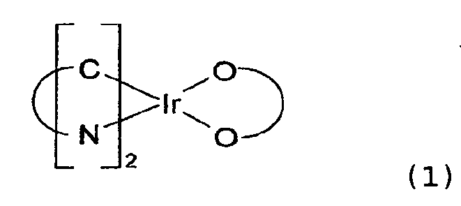
- To achieve these objects and other advantages and in accordance with the purpose of the invention, as embodied and broadly described herein, there is provided a red phosphorescent compound of Formula 1:
-

- wherein


 and 2,2-dimethyl-3,5-hexanedione
-

-


- Examples of preferred compounds that can be represented by Formula 1 include the following compounds:
-


-


- In another aspect of the present invention, there is provided a red phosphorescent compound of Formula 2:
-

- wherein


-


- Examples of preferred compounds that can be represented by Formula 2 include the following compounds:
-


-


- In another aspect of the present invention, there is provided a red phosphorescent compound of Formula 3:
-

- wherein


-


- Examples of preferred compounds that can be represented by Formula 3 include the following compounds:
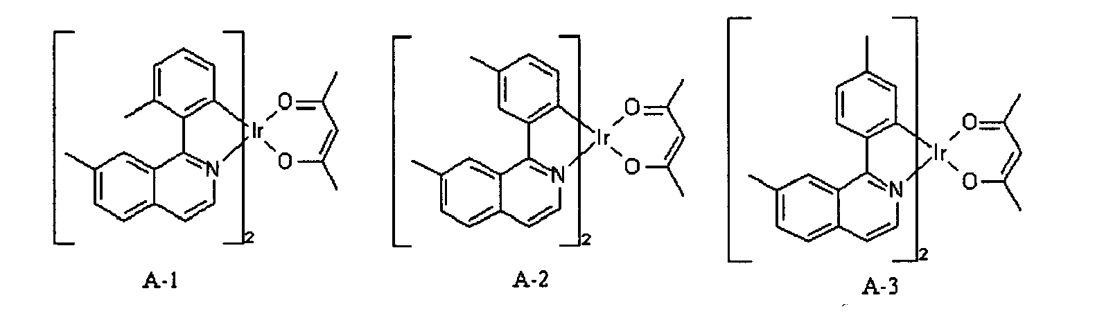
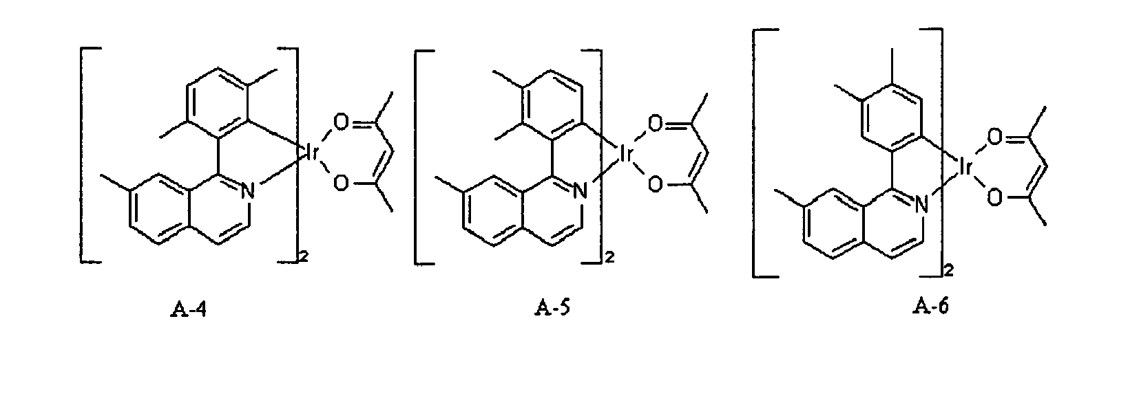


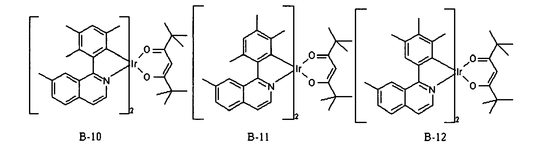
- In yet another aspect of the present invention, there is provided an organic electroluminescent (EL) device comprising an anode, a hole injecting layer (HIL), a hole transport layer (HTL), an light-emitting layer, an electron transport layer (ETL) and an electron injecting layer (EIL), and a cathode laminated in this order wherein one of the red phosphorescent compounds of Formulas 1 to 3 is used as a dopant of the light-emitting layer.
- A host used in the organic light-emitting layer of the organic EL device according to the present invention may be selected from Al complexes, Zn complexes, and carbazole derivatives. The dopant may be preferably used in an amount of 0.5 to 20% by weight, based on the weight of the host. When the dopant is used within this range, the desired effects of the organic EL device can be achieved. The Al and Zn complexes may have at least one ligand selected from quinolyl, biphenyl, isoquinolyl, phenyl, naphthyl, methylquinolyl, dimethylquinolyl and dimethylisoquinolyl groups. The carbazole derivatives may be preferably 4,4'-N,N' dicarbazole biphenyl (CBP).
- It is to be understood that both the foregoing general description and the following detailed description of the present invention are exemplary and explanatory and are intended to provide further explanation of the invention as claimed.
- The accompanying drawings, which are included to provide a further understanding of the invention and are incorporated in and constitute a part of this application, illustrate embodiment(s) of the invention and together with the description serve to explain the principle of the invention. In the drawings:
- FIG. 1 shows a graph showing a phenomenon wherein the color purity of an organic EL device becomes higher (i.e. as the x-values on CIE chromaticity coordinates increase), the relative sensitivity of the organic EL device decreases; and
- FIG. 2 shows the structural formulas of NPB, copper (II) phthalocyanine (CuPc), (btp)2Ir(acac), Alq3, BAlq and CBP used in Example Section according to the present invention.
- Reference will now be made in detail to the preferred embodiments of the present invention associated with red phosphorescent compounds and an organic electroluminescent (EL) device using one of the red phosphorescent compounds according to the present invention, examples of which are illustrated in the annexed drawings.
- Hereinafter, methods for synthesizing the red phosphorescent compounds represented by Formulas 1 to 3 for use in the organic EL devices according to the present invention will be described. First, a method for synthesizing iridium (III) (2-(3-methylphenyl)-4,7-dimethylquinolinato-N,C2') (2,4-pentanedionate-O,O) ("A-2"), which is a red phosphorescent compound represented by Formula 1, for use in an organic electroluminescent device.
- 1. Synthesis of 1-(3-methylphenyl)-4,7-dimethylisoquinoline

- N-(2-hydroxy-1-p-tolyl-propyl)-3-methylbezamide (2.1 mmol), phosphorus (V) oxide (10 mmol) and decahydronaphtalene (50 mmol) were put in a dried two-neck round-bottom flask. Then, the mixture was stirred at 120□ for 5 hours. After completion of the reaction, the reaction mixture was extracted with dichloromethane and water and distilled under reduced pressure. The resulting residue was purified by silica gel column chromatography. The eluate was distilled under reduced pressure. The residue was recrystallized from dichloromethane and petroleum ether, and filtered to yield 1-(3-methylphenyl)-4,7-dimethylisoquinoline.
- 2. Synthesis of dichloro-crosslinked dimer complex

- Iridium (III) chloride hydrate (1 mmol), the 1-(3-methylphenyl)-4,7-dimethylisoquinoline (2.5 mmol) and a mixed solvent (30 mL) of 2-ethoxyethanol and water (3 : 1) were put in a dried two-neck round-bottom flask. After the mixture was refluxed for 24 hours and water was added thereto to obtain a solid. The solid was filtered and washed with methanol and petroleum ether to yield the dichloro-crosslinked dimer complex.
- 3. Synthesis of iridium (III) (1-(3-methylphenyl)-4,7-dimethylisoquinolinato-N,C2')(2,4-pentanedionate-O,O)

- The dichloro-crosslinked dimer complex (1 mmol), 2,4-pentanedione (3 mmol), sodium carbonate (Na2CO3) (6 mmol) and 2-ethoxyethanol (30 mL) were put in a dried two-neck round-bottom flask. Then, the mixture was refluxed for 2 hours. The reaction mixture was allowed to cool to room temperature, and then distilled water was added thereto to obtain a solid. The solid was filtered and dissolved in dichloromethane. The solution was filtered through silica gel. The solvent was distilled off under reduced pressure and the resulting residue was washed with methanol and petroleum ether to yield to obtain the iridium (III) (1-(3-methylphenyl)-4,7-dimethylisoquinolinato-N,C2')(2,4-pentanedionate-O,O).
- Next, a method for synthesizing iridium (III) (2-(3'-methylphenyl)-4-methylisoquinolinato-N,C2')(2,4-pentanedionate-O,O) ("A-2"), which is a red phosphorescent compound represented by Formula 2, for use in an organic electroluminescent device.
- 1. Synthesis of 1-(3-methylphenyl)-4-methylisoquinoline

- 3-Methylphenyl borate (1.3 mmol), 2-chloro-4-methylquinoline (1 mmol), tetrakis(triphenylphosphine) palladium(O) (0.05 mmol) and potassium carbonate (3 mmol) were dissolved in THF (30 mL) and H2O (10 mL). The resulting solution was stirred in a bath at 100°C for 24 hours. After completion of the reaction, the solvents were removed. The reaction mixture was extracted with dichloromethane and water and distilled under reduced pressure. The resulting residue was purified by silica gel column chromatography. The eluate was distilled under reduced pressure. The residue was recrystallized from dichloromethane and petroleum ether, and filtered to yield 1-(3-methylphenyl)-4-methylisoquinoline as a solid.
- 2. Synthesis of dichloro-crosslinked dimer complex

- Iridium (III) chloride hydrate (1 mmol), the 1-(3-methylphenyl)-4-methylisoquinoline (2.5 mmol) and a mixed solvent (30 mL) of 2-ethoxyethanol and distilled water (3 : 1 (v/v) were put in a dried two-neck round-bottom flask. After the mixture was refluxed for 24 hours, water was added thereto to obtain a solid. The solid was filtered and washed with methanol and petroleum ether to yield the dichloro-crosslinked dimer complex.
- 3. Synthesis of iridium (III) (2-(3'-methylphenyl)-4-methylisoquinolinato-N,C2') (2,4-pentanedionate-O,O)

- The dichloro-crosslinked dimer complex (1 mmol), 2,4-pentanedione (3 mmol), sodium carbonate (Na2CO3) (6 mmol) and 2-ethoxyethanol (30 mL) were put in a dried two-neck round-bottom flask. Then, the mixture was refluxed for 24 hours. The reaction mixture was allowed to cool to room temperature, and then distilled water was added thereto to obtain a solid. The solid was filtered and dissolved in dichloromethane. The solution was filtered through silica gel. The solvent was distilled off under reduced pressure and the resulting residue was washed with methanol and petroleum ether to yield iridium (III) (2-(3'-methylphenyl)-4-methylisoquinolinato-N,C2')(2,4-pentanedionate-O,O).
- Lastly, a method for synthesizing iridium (III) (2-(3-methylphenyl)-7-methylisoquinolinato-N,C2')(2,4-pentanedionate-O,O) ("A-2"), which is a red phosphorescent compound represented by Formula 3, for use in an organic electroluminescent device.
- 1. Synthesis of 1-(3-methylphenyl)-7-methylisoquinoline

- Benzoic acid-(β -hydroxy-4-methyl-phenylamide) (2.1 mmol), phosphorus (V) oxide (10 mmol) and decahydronaphthalene (50 mmol) were put in a dried two-neck round-bottom flask. Then, the mixture was stirred at 120°C for 5 hours. After completion of the reaction, the reaction mixture was extracted with dichloromethane and water. The extract was distilled under reduced pressure. The resulting residue was purified by silica gel column chromatography. The eluate was distilled under reduced pressure. The residue was recrystallized from dichloromethane and petroleum ether and filtered to yield 1-(3-methylphenyl)-7-methylisoquinoline as a solid.
- 2. Synthesis of dichloro-crosslinked dimer complex
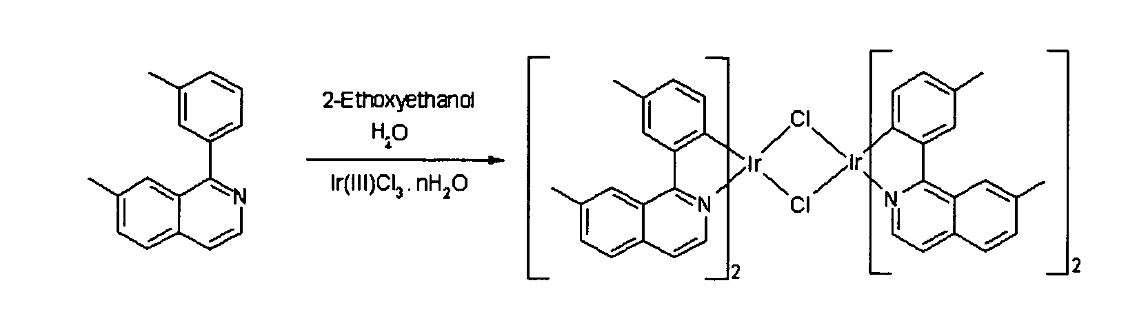
- Iridium (III) chloride hydrate (1 mmol), 1-(3-methylphenyl)-7-methylisoquinoline (2.5 mmol) and a mixed solvent (30 mL) of 2-ethoxyethanol and distilled water (3 : 1) were put in a dried two-neck round-bottom flask. After the mixture was refluxed for 24 hours, water was added thereto to obtain a solid. The solid was filtered and washed with methanol and petroleum ether to yield the dichloro-crosslinked dimer complex.
- 3. Synthesis of iridium (III) (1-(3-methylphenyl)-7-methylisoquinolinato-N,C2') (2,4-pentanedionate-O,O)

- The dichloro-crosslinked dimer complex (1 mmol), 2,4-pentanedione (3 mmol), sodium carbonate (Na2CO3) (6 mmol) and 2-ethoxyethanol (30 mL) were put in a dried two-neck round-bottom flask. Then, the mixture was stirred for 24 hours. After the mixture was allowed to cool to room temperature, distilled water was added thereto to obtain a solid. The solid was filtered and dissolved in dichloromethane. The solution was filtered through silica gel. The solvent was distilled off under reduced pressure and the residue was washed with methanol and petroleum ether to yield (1-(3-methylphenyl)-7-methylisoquinolinato-N, C2') (2,4-pentanedionate-O,O).
- Hereinafter, a detailed description will be made of preferred examples of the present invention. The invention is not to be construed as being limited to the examples.
- EXAMPLES A-1 to A-3 (Compounds of Formula 1) and Comparative Example A-1
- Example A-1
- An ITO-coated glass substrate was patterned to have a light-emitting area of 3 mm x 3 mm, followed by cleaning. After the patterned substrate was disposed in a vacuum chamber, the standard pressure of the chamber was adjusted to 1 x 10⁻⁶ torr. CuPc (200 Å), NPD (400 Å), BAlq + A-1 (7%) (200 Å), Alq3 (300 Å), LiF (5 Å) and Al (1000 Å) were sequentially deposited on the ITO glass substrate to fabricate an organic EL device.
- The luminance of the organic EL device was 801 cd/m2 at an electric current of 0.9 mA and a voltage of 6.6 V. At this time, the CIE chromaticity coordinates were x = 0.649 and y = 0.360. The lifetime (defined as the time taken before the luminance of the organic EL device decreases to half its initial value) of the organic EL device was 5,100 hours at 2,000 cd/m2.
- Example A-2
- An ITO-coated glass substrate was patterned to have a light-emitting area of 3 mm x 3 mm, followed by cleaning. After the patterned substrate was disposed in a vacuum chamber, the standard pressure of the chamber was adjusted to 1x10⁻⁶ torr. CuPc (200 Å), NPD (400 Å), BAlq + A-2 (7%) (200 Å), Alq3 (300 Å), LiF (5 Å) and Al (1000 Å) were sequentially deposited on the ITO glass substrate to fabricate an organic EL device.
- The luminance of the organic EL device was 795 cd/m2 at an electric current of 0.9 mA and a voltage of 6.3 V. At this time, the CIE chromaticity coordinates were x = 0.650 and y = 0.361. The lifetime (defined as the time taken before the luminance of the organic EL device decreases to half its initial value) of the organic EL device was 4,800 hours at 2,000 cd/m2.
- Example A-3
- An ITO-coated glass substrate was patterned to have a light-emitting area of 3 mm x 3 mm, followed by cleaning. After the patterned substrate was disposed in a vacuum chamber, the standard pressure of the chamber was adjusted to 1 x 10⁻⁶ torr. CuPc (200 Å), NPD (400 Å), BAlq + A-7 (7%) (200 Å), Alq3 (300 Å), LiF (5 Å) and A1 (1000 Å) were sequentially deposited on the ITO glass substrate to fabricate an organic EL device.
- The luminance of the organic EL device was 783 cd/m2 at an electric current of 0.9 mA and a voltage of 6.1 V. At this time, the CIE chromaticity coordinates were x = 0.651 and y = 0.362. The lifetime (defined as the time taken before the luminance of the organic EL device decreases to half its initial value) of the organic EL device was 5,500 hours at 2,000 cd/m2.
- Example A-4
- An ITO-coated glass substrate was patterned to have a light-emitting area of 3 mm x 3 mm, followed by cleaning. The patterned substrate was disposed in a vacuum chamber. Then, the standard pressure of the chamber was adjusted to 1x10⁻⁶ torr. CuPc (200 Å), NPD (400 Å), BAlq + B-2 (7%) (200 Å), a hole blocking layer (100 Å), Alq3 (300 Å), LiF (5 Å) and Al (1000 Å) were sequentially deposited on the ITO glass substrate to manufacture an organic EL device.
- When BAlq was used as a material for the hole blocking layer, the luminance of the organic EL device was 768 cd/m2 at an electric current of 0.9 mA and a voltage of 6.0 V. At this time, the CIE chromaticity coordinates were x = 0.652, y = 0.361. The lifetime (defined as the time taken before the luminance of the organic EL device decreases to half its initial value) of the organic EL device was 4,000 hours at 2,000 cd/m2.
- Example A-5
- An ITO-coated glass substrate was patterned to have a light-emitting area of 3 mm x 3 mm, followed by cleaning. The patterned substrate was disposed in a vacuum chamber. Then, the standard pressure of the chamber was adjusted to 1x10⁻⁶ torr. CuPc (200 Å), NPD (400 Å), BAlq + B-7 (7%) (200 Å), a hole blocking layer (100 Å), Alq3 (300 Å), LiF (5 Å) and Al (1000 Å) were sequentially deposited on the ITO glass substrate to manufacture an organic EL device.
- When BAlq was used as a material for the hole blocking layer, the luminance of the organic EL device was 753 cd/m2 at an electric current of 0.9 mA and a voltage of 6.0 V. At this time, the CIE chromaticity coordinates were x = 0.652 and y = 0.362. The lifetime (defined as the time taken before the luminance of the organic EL device decreases to half its initial value) of the organic EL device was 4,000 hours at 2,000 cd/m2.
- Comparative Example A-1
- An ITO-coated glass substrate was patterned to have a light-emitting area of 3 mm x 3 mm, followed by cleaning. The patterned substrate was disposed in a vacuum chamber. Then, the standard pressure of the chamber was adjusted to 1X10⁻⁶ torr. CuPc (200 Å), NPD (400 Å), BAlq + (btp)2Ir(acac) (7%) (200 Å), Alq3 (300 Å), LiF (5 Å) and Al (1000 Å) were sequentially deposited on the ITO glass substrate to manufacture an EL device.
- The luminance of the organic EL device was 780 cd/m2 at an electric current of 0.9 mA and a voltage of 7.5 V. At this time, the CIE chromaticity coordinates were x = 0.659 and y = 0.329. The lifetime (defined as the time taken before the luminance of the organic EL device decreases to half its initial value) of the organic EL device was 2,500 hours at 2,000 cd/m2.
- The organic EL devices fabricated in Examples A-1 to A-5 and Comparative Example A-1 were evaluated for efficiency, CIE chromaticity coordinates, luminance and lifetime characteristics. The results are shown in Table 1.
-
TABLE 1 Device Voltage (V) Electric current (mA) Luminance (cd/m2) Current efficiency (cd/A) Power efficiency (1m/W) CIE (X) CIE (Y) Life time (h) (half the initial luminance) Ex. A-1 6.6 0.9 801 8.01 3.81 0.649 0.360 5,100 Ex. A-2 6.3 0.9 795 7.95 3.96 0.650 0.361 4,800 Ex. A-3 6.1 0.9 783 7.83 4.03 0.651 0.362 5,500 Ex. A-4 6.0 0.9 768 7.68 4.02 0.652 0.361 4,000 Ex. A-5 6.0 0.9 753 7.53 3.94 0.652 0.362 4,000 Comp. Ex. A-1 7.5 0.9 780 7.80 3.27 0.659 0.329 2,500 - Examples B-1 to B-5 (Compounds of Formula 2) and Comparative Example B-1
- Example B-1
- An ITO-coated glass substrate was patterned to have a light-emitting area of 3 mm x 3 mm, followed by cleaning. After the patterned substrate was disposed in a vacuum chamber, the standard pressure of the chamber was adjusted to 1x10⁻⁶ torr. CuPc (200 Å), NPD (400 Å), BAlq + A-2 (7%) (200 Å), Alq3 (300 Å), LiF (5 Å) and Al (1000 Å) were sequentially deposited on the ITO glass substrate to fabricate an organic EL device.
- The luminance of the organic EL device was 1,115 cd/m2 at an electric current of 0.9 mA and a voltage of 6.4 V. At this time, the CIE chromaticity coordinates were x = 0.646 and y = 0.356. The lifetime (defined as the time taken before the luminance of the organic EL device decreases to half its initial value) of the organic EL device was 5,000 hours at 2,000 cd/m2.
- Example B-2
- An ITO-coated glass substrate was patterned to have a light-emitting area of 3 mm x 3 mm, followed by cleaning. After the patterned substrate was disposed in a vacuum chamber, the standard pressure of the chamber was adjusted to 1x10⁻⁶ torr. CuPc (200 Å), NPD (400 Å), BAlq + A-5 (7%) (200 Å), Alq3 (300 Å), LiF (5 Å) and Al (1000 Å) were sequentially deposited on the ITO glass substrate to fabricate an organic EL device.
- The luminance of the organic EL device was 1,032 cd/m2 at an electric current of 0.9 mA and a voltage of 6.2 V. At this time, the CIE chromaticity coordinates were x = 0.647 and y = 0.358. The lifetime (defined as the time taken before the luminance of the organic EL device decreases to half its initial value) of the organic EL device was 4,600 hours at 2,000 cd/m2.
- Example B-3
- An ITO-coated glass substrate was patterned to have a light-emitting area of 3 mm x 3 mm, followed by cleaning. After the patterned substrate was disposed in a vacuum chamber, the standard pressure of the chamber was adjusted to 1x10⁻⁶ torr. CuPc (200 Å), NPD (400 Å), BAlq + A-7 (7%) (200 Å), Alq3 (300 Å), LiF (5 Å) and Al (1000 Å) were sequentially deposited on the ITO glass substrate to fabricate an organic EL device.
- The luminance of the organic EL device was 963 cd/m2 at an electric current of 0.9 mA and a voltage of 5.3 V. At this time, the CIE chromaticity coordinates were x = 0.649 and y = 0.359. The lifetime (defined as the time taken before the luminance of the organic EL device decreases to half its initial value) of the organic EL device was 4,100 hours at 2,000 cd/m2.
- Example B-4
- An ITO-coated glass substrate was patterned to have a light-emitting area of 3 mm x 3 mm, followed by cleaning. After the patterned substrate was disposed in a vacuum chamber, the standard pressure of the chamber was adjusted to 1x10⁻⁶ torr. CuPc (200 Å), NPD (400 Å), BAlq + B-2 (7%) (200 Å), Alq3 (300 Å), LiF (5 Å) and Al (1000 Å) were sequentially deposited on the ITO glass substrate to fabricate an organic EL device.
- The luminance of the organic EL device was 932 cd/m2 at an electric current of 0.9 mA and a voltage of 6.3 V. At this time, the CIE chromaticity coordinates were x = 0.647 and y = 0.360. The lifetime (defined as the time taken before the luminance of the organic EL device decreases to half its initial value) of the organic EL device was 3,100 hours at 2,000 cd/m2.
- Example B-5
- An ITO-coated glass substrate was patterned to have a light-emitting area of 3 mm x 3 mm, followed by cleaning. After the patterned substrate was disposed in a vacuum chamber, the standard pressure of the chamber was adjusted to 1x10⁻⁶ torr. CuPc (200 Å), NPD (400 Å), BAlq + B-5 (7%) (200 Å), Alq3 (300 Å), LiF (5 Å) and Al (1000 Å) were sequentially deposited on the ITO glass substrate to fabricate an organic EL device.
- The luminance of the organic EL device was 911 cd/m2 at an electric current of 0.9 mA and a voltage of 6.6 V. At this time, the CIE chromaticity coordinates were x = 0.647 and y = 0.358. The lifetime (defined as the time taken before the luminance of the organic EL device decreases to half its initial value) of the organic EL device was 3,150 hours at 2,000 cd/m2.
- Comparative Example B-1
- An ITO-coated glass substrate was patterned to have a light-emitting area of 3 mm x 3 mm, followed by cleaning. After the patterned substrate was disposed in a vacuum chamber, the standard pressure of the chamber was adjusted to 1x10⁻⁶ torr. CuPc (200 Å), NPD (400 Å), BAlq + (btp)2Ir(acac) (7%) (200 Å), Alq3 (300 Å), LiF (5 Å) and Al (1000 Å) were sequentially deposited on the ITO glass substrate to manufacture an organic EL device.
- The luminance of the organic EL device was 780 cd/m2 at an electric current of 0.9 mA and a voltage of 7.5 V. At this time, the CIE chromaticity coordinates were x = 0.659 and y = 0.329. The lifetime (defined as the time taken before the luminance of the organic EL device decreases to half its initial value) of the organic EL device was 2,500 hours at 2,000 cd/m2.
- The organic EL devices fabricated in Examples B-1 to B-5 and Comparative Example B-1 were evaluated for efficiency, CIE chromaticity coordinates, luminance and lifetime characteristics. The results are shown in Table 2.
-
TABLE 2 Device Voltage (V) Electric current (mA) Luminance (cd/m2) Current efficiency (cd/A) Power efficiency (1m/W) CIE (X) CIE (Y) Life time (h) (half the initial luminance) Ex. B-1 6.4 0.9 1,115 11.15 5.47 0.646 0.356 5,000 Ex. B-2 6.2 0.9 1,032 10.32 5.23 0.647 0.351 4,600 Ex. B-3 6.1 0.9 963 9.63 4.96 0.649 0.359 4,100 Ex. B-4 6.3 0.9 932 9.32 4.65 0.647 0.360 3,100 Ex. B-5 6.6 0.9 911 9.11 4.33 0.647 0.358 3,150 Comp. Ex. B-1 7.5 0.9 780 7.80 3.27 0.659 0.329 2,500 - Examples C-1 to C-6 (Compounds of Formula 3) and Comparative Example C-1
- Example C-1
- An ITO-coated glass substrate was patterned to have a light-emitting area of 3 mm x 3 mm, followed by cleaning. After the patterned substrate was disposed in a vacuum chamber, the standard pressure of the chamber was adjusted to 1x10⁻⁶ torr. CuPc (200 Å), NPD (400 Å), BAlq + A-1 (7%) (200 Å), Alq3 (300 Å), LiF (5 Å) and Al (1000 Å) were sequentially deposited on the ITO glass substrate to fabricate an organic EL device.
- The luminance of the organic EL device was 801 cd/m2 at an electric current of 0.9 mA and a voltage of 6.6 V. At this time, the CIE chromaticity coordinates were x = 0.649 and y = 0.360. The lifetime (defined as the time taken before the luminance of the organic EL device decreases to half its initial value) of the organic EL device was 5,100 hours at 2,000 cd/m2.
- Example C-2
- An ITO-coated glass substrate was patterned to have a light-emitting area of 3 mm x 3 mm, followed by cleaning. After the patterned substrate was disposed in a vacuum chamber, the standard pressure of the chamber was adjusted to 1x10⁻⁶ torr. CuPc (200 Å), NPD (400 Å), BAlq + A-2 (7%) (200 Å), Alq3 (300 Å), LiF (5 Å) and Al (1000 Å) were sequentially deposited on the ITO glass substrate to fabricate an organic EL device.
- The luminance of the organic EL device was 795 cd/m2 at an electric current of 0.9 mA and a voltage of 6.3 V. At this time, the CIE chromaticity coordinates were x = 0.650 and y = 0.361. The lifetime (defined as the time taken before the luminance of the organic EL device decreases to half its initial value) of the organic EL device was 4,800 hours at 2,000 cd/m2.
- Example C-3
- An ITO-coated glass substrate was patterned to have a light-emitting area of 3 mm x 3 mm, followed by cleaning. After the patterned substrate was disposed in a vacuum chamber, the standard pressure of the chamber was adjusted to 1x10⁻⁶ torr. CuPc (200 Å), NPD (400 Å), BAlq + A-7 (7%) (200 Å), Alq3 (300 Å), LiF (5 Å) and Al (1000 Å) were sequentially deposited on the ITO glass substrate to fabricate an organic EL device.
- The luminance of the organic EL device was 783 cd/m2 at an electric current of 0.9 mA and a voltage of 6.1 V. At this time, the CIE chromaticity coordinates were x = 0.651 and y = 0.362. The lifetime (defined as the time taken before the luminance of the organic EL device decreases to half its initial value) of the organic EL device was 5,500 hours at 2,000 cd/m2.
- Example C-4
- An ITO-coated glass substrate was patterned to have a light-emitting area of 3 mm x 3 mm, followed by cleaning. After the patterned substrate was disposed in a vacuum chamber, the standard pressure of the chamber was adjusted to 1x10⁻⁶ torr. CuPc (200 Å), NPD (400 Å), BAlq + B-2 (7%) (200 Å), Alq3 (300 Å), LiF (5 Å) and Al (1000 Å) were sequentially deposited on the ITO glass substrate to fabricate an organic EL device.
- The luminance of the organic EL device was 768 cd/m2 at an electric current of 0.9 mA and a voltage of 6.0 V. At this time, the CIE chromaticity coordinates were x = 0.652 and y = 0.361. The lifetime (defined as the time taken before the luminance of the organic EL device decreases to half its initial value) of the organic EL device was 4,000 hours at 2,000 cd/m2.
- Example C-5
- An ITO-coated glass substrate was patterned to have a light-emitting area of 3 mm x 3 mm, followed by cleaning. After the patterned substrate was disposed in a vacuum chamber, the standard pressure of the chamber was adjusted to 1x10⁻⁶ torr. CuPc (200 Å), NPD (400 Å), BAlq + B-7 (7%) (200 Å), Alq3 (300 Å), LiF (5 Å) and Al (1000 Å) were sequentially deposited on the ITO glass substrate to fabricate an organic EL device.
- The luminance of the organic EL device was 753 cd/m2 at an electric current of 0.9 mA and a voltage of 6.0 V. At this time, the CIE chromaticity coordinates were x = 0.652 and y = 0.362. The lifetime (defined as the time taken before the luminance of the organic EL device decreases to half its initial value) of the organic EL device was 4,000 hours at 2,000 cd/m2.
- Comparative Example C-1
- An ITO-coated glass substrate was patterned to have a light-emitting area of 3 mm x 3 mm, followed by cleaning. After the patterned substrate was disposed in a vacuum chamber, the standard pressure of the chamber was adjusted to 1x10⁻⁶ torr. CuPc (200 Å), NPD (400 Å), BAlq + (btp)2Ir(acac) (7%) (200 Å), Alq3 (300 Å), LiF (5 Å) and Al (1000 Å) were sequentially deposited on the ITO glass substrate to manufacture an organic EL device.
- The luminance of the organic EL device was 780 cd/m2 at an electric current of 0.9 mA and a voltage of 7.5 V. At this time, the CIE chromaticity coordinates were x = 0.659 and y = 0.329. The lifetime (defined as the time taken before the luminance of the organic EL device decreases to half its initial value) of the organic EL device was 2,500 hours at 2,000 cd/m2.
- The organic EL devices fabricated in Examples C-1 to C-5 and Comparative Example C-1 were evaluated for efficiency, CIE chromaticity coordinates, luminance and lifetime characteristics. The results are shown in Table 3.
-
TABLE 3 Device Voltage (V) Electric current (mA) Luminance (cd/m2) Current efficiency (cd/A) Power efficiency (1m/W) CIE (X) CIE (Y) Life time (h) (half the initial luminance) Ex. C-1 6.6 0.9 801 8.01 3.81 0.649 0.360 5,100 Ex. C-2 6.3 0.9 795 7.95 3.96 0.650 0.351 4,800 Ex. C-3 6.1 0.9 783 7.83 4.03 0.651 0.362 5,500 Ex. C-4 6.0 0.9 768 7.68 4.02 0.652 0.361 4,000 Ex. C-5 6.0 0.9 753 7.53 3.94 0.652 0.362 4,000 Comp. Ex. C-1 7.5 0.9 780 7.80 3.27 0.659 0.329 2,500 - It will be apparent to those skilled in the art that various modifications and variations can be made in the present invention without departing from the spirit or scope of the inventions. Thus, it is intended that the present invention covers the modifications and variations of this invention provided they come within the scope of the appended claims and their equivalents.
Claims (6)
- A red phosphorescent compound of Formula 1 below:

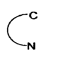

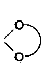
- A red phosphorescent compound of Formula 2 below:


- A red phosphorescent compound of Formula 3 below:


- An organic electroluminescent (EL) device comprising an anode, a hole injecting layer, a hole transport layer, a light-emitting layer, an electron transport layer, an electron injecting layer, and a cathode laminated in this order wherein the red phosphorescent compound according to any one of claims 1 to 3 is used as a dopant of the light-emitting layer and is present in an amount of 0.5 to 20% by weight, based on the weight of a host.
- The organic electroluminescent (EL) device according to claim 4, wherein the host is selected from an Al complex, a Zn complex, and a carbazole derivative.
- The organic electroluminescent (EL) device according to claim 5, wherein the A1 or Zn complex has at least one ligand selected from quinolyl, biphenyl, isoquinolyl, phenyl, naphthyl, methylquinolyl, dimethylquinolyl and dimethylisoquinolyl groups, and the carbazole derivative is 4, 4'-N,N' dicarbazole biphenyl (CBP).
Applications Claiming Priority (3)
| Application Number | Priority Date | Filing Date | Title |
|---|---|---|---|
| KR1020050105981A KR100662379B1 (en) | 2005-11-07 | 2005-11-07 | Red phosphorescent compound and organic light emitting device using the same |
| KR1020060037102A KR20070105080A (en) | 2006-04-25 | 2006-04-25 | Red phosphorescent compound and organic light emitting device using the same |
| KR1020060037101A KR20070105079A (en) | 2006-04-25 | 2006-04-25 | Red phosphorescent compound and organic light emitting device using the same |
Publications (2)
| Publication Number | Publication Date |
|---|---|
| EP1784057A1 true EP1784057A1 (en) | 2007-05-09 |
| EP1784057B1 EP1784057B1 (en) | 2014-05-07 |
Family
ID=37714394
Family Applications (1)
| Application Number | Title | Priority Date | Filing Date |
|---|---|---|---|
| EP06023132.1A Active EP1784057B1 (en) | 2005-11-07 | 2006-11-07 | Red phosphorescent compounds and organic electroluminescent devices using the same |
Country Status (2)
| Country | Link |
|---|---|
| US (1) | US8501328B2 (en) |
| EP (1) | EP1784057B1 (en) |
Cited By (4)
| Publication number | Priority date | Publication date | Assignee | Title |
|---|---|---|---|---|
| JP2013121957A (en) * | 2011-12-09 | 2013-06-20 | Universal Display Corp | Novel organic light-emitting material |
| CN103965261A (en) * | 2013-01-31 | 2014-08-06 | 海洋王照明科技股份有限公司 | Red light organic electrophosphorescence material metal iridium coordination compound and preparation method thereof, and organic electroluminescent device |
| CN103965262A (en) * | 2013-01-31 | 2014-08-06 | 海洋王照明科技股份有限公司 | Red light organic electrophosphorescence material metal iridium coordination compound and preparation method thereof, and organic electroluminescent device |
| CN103965256A (en) * | 2013-01-31 | 2014-08-06 | 海洋王照明科技股份有限公司 | Red light organic electrophosphorescence material metal iridium coordination compound and preparation method thereof, and organic electroluminescent device |
Families Citing this family (10)
| Publication number | Priority date | Publication date | Assignee | Title |
|---|---|---|---|---|
| US9023489B2 (en) * | 2005-11-07 | 2015-05-05 | Lg Display Co., Ltd. | Red phosphorescent compounds and organic electroluminescent devices using the same |
| TWI510598B (en) * | 2007-03-08 | 2015-12-01 | Universal Display Corp | Phosphorescent materials |
| US10749118B2 (en) | 2014-06-26 | 2020-08-18 | Samsung Display Co., Ltd. | Heterocyclic compound and organic light-emitting device including the same |
| CN110343136B (en) | 2018-04-02 | 2023-08-11 | 三星电子株式会社 | Organometallic compound, and organic light-emitting device and diagnostic composition comprising same |
| JP7336865B2 (en) | 2018-04-02 | 2023-09-01 | 三星電子株式会社 | Organometallic compounds, organic light-emitting devices containing the same, and diagnostic compositions |
| KR102206820B1 (en) * | 2018-05-14 | 2021-01-22 | 주식회사 엘지화학 | Compound and organic light emitting device comprising the same |
| EP3604321B1 (en) | 2018-07-31 | 2022-02-09 | Samsung Electronics Co., Ltd. | Organometallic compound, organic light-emitting device including the same, and diagnostic composition including the organometallic compound |
| EP3617216B1 (en) | 2018-08-31 | 2021-12-01 | Samsung Electronics Co., Ltd. | Organometallic compound, organic light-emitting device including the same, and diagnostic composition including the organometallic compound |
| EP3653608A1 (en) | 2018-11-19 | 2020-05-20 | Ludwig-Maximilians-Universität München | Isoquinoline biaryl compounds, a pharmaceutical composition comprising the same, and uses thereof |
| KR102787165B1 (en) | 2019-04-17 | 2025-03-26 | 삼성전자주식회사 | Organometallic compound, organic light emitting device including the same and a composition for diagnosing including the same |
Citations (3)
| Publication number | Priority date | Publication date | Assignee | Title |
|---|---|---|---|---|
| WO2003040256A2 (en) | 2001-11-07 | 2003-05-15 | E.I. Du Pont De Nemours And Company | Electroluminescent iridium compounds having red-orange or red emission and devices made with such compounds |
| CN1582073A (en) * | 2004-02-27 | 2005-02-16 | 清华大学 | A kind of organic electrophosphorescent device and its preparation method |
| WO2006014599A2 (en) * | 2004-07-07 | 2006-02-09 | Universal Display Corporation | Stable and efficient electroluminescent materials |
Family Cites Families (3)
| Publication number | Priority date | Publication date | Assignee | Title |
|---|---|---|---|---|
| US6893743B2 (en) * | 2000-10-04 | 2005-05-17 | Mitsubishi Chemical Corporation | Organic electroluminescent device |
| KR100865096B1 (en) * | 2000-11-30 | 2008-10-24 | 캐논 가부시끼가이샤 | Light emitting element and display device |
| US6835469B2 (en) | 2001-10-17 | 2004-12-28 | The University Of Southern California | Phosphorescent compounds and devices comprising the same |
-
2006
- 2006-11-06 US US11/593,146 patent/US8501328B2/en active Active
- 2006-11-07 EP EP06023132.1A patent/EP1784057B1/en active Active
Patent Citations (3)
| Publication number | Priority date | Publication date | Assignee | Title |
|---|---|---|---|---|
| WO2003040256A2 (en) | 2001-11-07 | 2003-05-15 | E.I. Du Pont De Nemours And Company | Electroluminescent iridium compounds having red-orange or red emission and devices made with such compounds |
| CN1582073A (en) * | 2004-02-27 | 2005-02-16 | 清华大学 | A kind of organic electrophosphorescent device and its preparation method |
| WO2006014599A2 (en) * | 2004-07-07 | 2006-02-09 | Universal Display Corporation | Stable and efficient electroluminescent materials |
Non-Patent Citations (8)
| Title |
|---|
| DATABASE CA [online] CHEMICAL ABSTRACTS SERVICE, COLUMBUS, OHIO, US; QIU, YONG ET AL: "Method for manufacturing organic electrophosphorescent device", XP002422602, retrieved from STN Database accession no. 145:220753 * |
| FANG ET AL., INORGANICA CHIMICA ACTA, vol. 359, no. 2, 2006, pages 441 - 450 |
| FANG K-H ET AL: "Color tuning of iridium complexes - Part I: Substituted phenylisoquinoline-based iridium complexes as the triplet emitter", INORGANICA CHIMICA ACTA, vol. 359, no. 2, 20 January 2006 (2006-01-20), pages 441 - 450, XP005232525, ISSN: 0020-1693 * |
| HUANG Y-T ET AL: "Bi-substituted Effect on Phenylisoquinoline Iridium(III) Complexes", ORGANOMETALLICS, vol. 24, no. 25, 2005, pages 6230 - 6238, XP009079764, ISSN: 0276-7333 * |
| LEE Y H ET AL: "Theoretical study of Ir(III) complexes of fluorinated phenylbenzoquinoline as red phosphorescent material", JAPANESE JOURNAL OF APPLIED PHYSICS, PART 1: REGULAR PAPERS, BRIEF COMMUNICATIONS & REVIEW PAPERS, vol. 45, no. 1B, 2006, pages 563 - 567, XP009079763 * |
| LI C-L ET AL: "Yellow and red electrophosphors based on linkage isomers of phenylisoquinolinyliridium complexes: distinct differences in photophysical and electroluminescence properties", ADVANCED FUNCTIONAL MATERIALS, vol. 15, no. 3, March 2005 (2005-03-01), pages 387 - 395, XP001224595, ISSN: 1616-301X * |
| YANG C-H ET AL: "Color tuning of iridium complexes for organic light-emitting diodes: The electronegative effect and pi-conjugation effect", JOURNAL OF ORGANOMETALLIC CHEMISTRY, vol. 691, no. 12, 1 June 2006 (2006-06-01), pages 2767 - 2773, XP005429595, ISSN: 0022-328X * |
| YANG C-H ET AL: "Synthesis of a high-efficiency red phosphorescent emitter for organic light-emitting diodes", JOURNAL OF MATERIALS CHEMISTRY, vol. 14, no. 6, 2004, pages 947 - 950, XP009079766, ISSN: 0959-9428 * |
Cited By (9)
| Publication number | Priority date | Publication date | Assignee | Title |
|---|---|---|---|---|
| JP2013121957A (en) * | 2011-12-09 | 2013-06-20 | Universal Display Corp | Novel organic light-emitting material |
| US9512355B2 (en) | 2011-12-09 | 2016-12-06 | Universal Display Corporation | Organic light emitting materials |
| JP2017014275A (en) * | 2011-12-09 | 2017-01-19 | ユニバーサル ディスプレイ コーポレイション | Novel organic light emitting materials |
| TWI642758B (en) * | 2011-12-09 | 2018-12-01 | 美商環球展覽公司 | Novel organic luminescent materials |
| US10454046B2 (en) | 2011-12-09 | 2019-10-22 | Universal Display Corporation | Organic electroluminescent materials and devices |
| US11482684B2 (en) | 2011-12-09 | 2022-10-25 | Universal Display Corporation | Organic electroluminescent materials and devices |
| CN103965261A (en) * | 2013-01-31 | 2014-08-06 | 海洋王照明科技股份有限公司 | Red light organic electrophosphorescence material metal iridium coordination compound and preparation method thereof, and organic electroluminescent device |
| CN103965262A (en) * | 2013-01-31 | 2014-08-06 | 海洋王照明科技股份有限公司 | Red light organic electrophosphorescence material metal iridium coordination compound and preparation method thereof, and organic electroluminescent device |
| CN103965256A (en) * | 2013-01-31 | 2014-08-06 | 海洋王照明科技股份有限公司 | Red light organic electrophosphorescence material metal iridium coordination compound and preparation method thereof, and organic electroluminescent device |
Also Published As
| Publication number | Publication date |
|---|---|
| US20070128468A1 (en) | 2007-06-07 |
| EP1784057B1 (en) | 2014-05-07 |
| US8501328B2 (en) | 2013-08-06 |
Similar Documents
| Publication | Publication Date | Title |
|---|---|---|
| EP1783133B1 (en) | Red phosphorescent compound and organic electroluminescent device using the same | |
| EP1783132B1 (en) | Red phosphorescent compounds and organic electromuninescent devices using the same | |
| EP1856226B1 (en) | Red phosphorescent compounds and organic electroluminescence devices using the same | |
| EP1856227B1 (en) | Red phosphorescence compounds and organic electroluminescence devices using the same | |
| US8623519B2 (en) | Red phosphorescent compound and organic electroluminescent device using the same | |
| EP2267097B1 (en) | Improved electroluminescent stability | |
| EP1784057B1 (en) | Red phosphorescent compounds and organic electroluminescent devices using the same | |
| CN101397311A (en) | Red phosphorescent compound and organic electroluminescent device using the same | |
| KR101630317B1 (en) | Red phosphorescence compound and Organic Electroluminescence Device using the same | |
| KR20070105080A (en) | Red phosphorescent compound and organic light emitting device using the same | |
| KR100662379B1 (en) | Red phosphorescent compound and organic light emitting device using the same | |
| KR101493218B1 (en) | Red phosphorescent compound and organic electroluminescent device using the same | |
| KR100662430B1 (en) | Red phosphorescent compound and organic light emitting device using the same | |
| KR100662377B1 (en) | Red phosphorescent compound and organic light emitting device using the same | |
| KR100747572B1 (en) | Red phosphorescent compound and organic light emitting device using the same | |
| CN109206457A (en) | Red phosphorescent compound and the organic electroluminescence device for using the compound | |
| KR20070105079A (en) | Red phosphorescent compound and organic light emitting device using the same | |
| CN110627836A (en) | Red phosphorescent compound and organic electroluminescent device using the same | |
| CN109485678A (en) | Red phosphorescent compound and the organic electroluminescence device for using the compound | |
| KR20070097138A (en) | Red phosphorescent compound and organic light emitting device using the same |
Legal Events
| Date | Code | Title | Description |
|---|---|---|---|
| PUAI | Public reference made under article 153(3) epc to a published international application that has entered the european phase |
Free format text: ORIGINAL CODE: 0009012 |
|
| 17P | Request for examination filed |
Effective date: 20061107 |
|
| AK | Designated contracting states |
Kind code of ref document: A1 Designated state(s): AT BE BG CH CY CZ DE DK EE ES FI FR GB GR HU IE IS IT LI LT LU LV MC NL PL PT RO SE SI SK TR |
|
| AX | Request for extension of the european patent |
Extension state: AL BA HR MK YU |
|
| 17Q | First examination report despatched |
Effective date: 20071119 |
|
| AKX | Designation fees paid |
Designated state(s): AT BE BG CH CY CZ DE DK EE ES FI FR GB GR HU IE IS IT LI LT LU LV MC NL PL PT RO SE SI SK TR |
|
| RAP1 | Party data changed (applicant data changed or rights of an application transferred) |
Owner name: LG DISPLAY CO., LTD. |
|
| GRAJ | Information related to disapproval of communication of intention to grant by the applicant or resumption of examination proceedings by the epo deleted |
Free format text: ORIGINAL CODE: EPIDOSDIGR1 |
|
| GRAP | Despatch of communication of intention to grant a patent |
Free format text: ORIGINAL CODE: EPIDOSNIGR1 |
|
| INTG | Intention to grant announced |
Effective date: 20140102 |
|
| GRAS | Grant fee paid |
Free format text: ORIGINAL CODE: EPIDOSNIGR3 |
|
| GRAA | (expected) grant |
Free format text: ORIGINAL CODE: 0009210 |
|
| AK | Designated contracting states |
Kind code of ref document: B1 Designated state(s): AT BE BG CH CY CZ DE DK EE ES FI FR GB GR HU IE IS IT LI LT LU LV MC NL PL PT RO SE SI SK TR |
|
| REG | Reference to a national code |
Ref country code: GB Ref legal event code: FG4D |
|
| REG | Reference to a national code |
Ref country code: AT Ref legal event code: REF Ref document number: 667506 Country of ref document: AT Kind code of ref document: T Effective date: 20140515 |
|
| REG | Reference to a national code |
Ref country code: IE Ref legal event code: FG4D |
|
| REG | Reference to a national code |
Ref country code: DE Ref legal event code: R096 Ref document number: 602006041399 Country of ref document: DE Effective date: 20140618 |
|
| REG | Reference to a national code |
Ref country code: AT Ref legal event code: MK05 Ref document number: 667506 Country of ref document: AT Kind code of ref document: T Effective date: 20140507 |
|
| REG | Reference to a national code |
Ref country code: NL Ref legal event code: VDEP Effective date: 20140507 |
|
| REG | Reference to a national code |
Ref country code: LT Ref legal event code: MG4D |
|
| PG25 | Lapsed in a contracting state [announced via postgrant information from national office to epo] |
Ref country code: IS Free format text: LAPSE BECAUSE OF FAILURE TO SUBMIT A TRANSLATION OF THE DESCRIPTION OR TO PAY THE FEE WITHIN THE PRESCRIBED TIME-LIMIT Effective date: 20140907 Ref country code: LT Free format text: LAPSE BECAUSE OF FAILURE TO SUBMIT A TRANSLATION OF THE DESCRIPTION OR TO PAY THE FEE WITHIN THE PRESCRIBED TIME-LIMIT Effective date: 20140507 Ref country code: GR Free format text: LAPSE BECAUSE OF FAILURE TO SUBMIT A TRANSLATION OF THE DESCRIPTION OR TO PAY THE FEE WITHIN THE PRESCRIBED TIME-LIMIT Effective date: 20140808 Ref country code: FI Free format text: LAPSE BECAUSE OF FAILURE TO SUBMIT A TRANSLATION OF THE DESCRIPTION OR TO PAY THE FEE WITHIN THE PRESCRIBED TIME-LIMIT Effective date: 20140507 Ref country code: CY Free format text: LAPSE BECAUSE OF FAILURE TO SUBMIT A TRANSLATION OF THE DESCRIPTION OR TO PAY THE FEE WITHIN THE PRESCRIBED TIME-LIMIT Effective date: 20140507 |
|
| PG25 | Lapsed in a contracting state [announced via postgrant information from national office to epo] |
Ref country code: ES Free format text: LAPSE BECAUSE OF FAILURE TO SUBMIT A TRANSLATION OF THE DESCRIPTION OR TO PAY THE FEE WITHIN THE PRESCRIBED TIME-LIMIT Effective date: 20140507 Ref country code: AT Free format text: LAPSE BECAUSE OF FAILURE TO SUBMIT A TRANSLATION OF THE DESCRIPTION OR TO PAY THE FEE WITHIN THE PRESCRIBED TIME-LIMIT Effective date: 20140507 Ref country code: PL Free format text: LAPSE BECAUSE OF FAILURE TO SUBMIT A TRANSLATION OF THE DESCRIPTION OR TO PAY THE FEE WITHIN THE PRESCRIBED TIME-LIMIT Effective date: 20140507 Ref country code: LV Free format text: LAPSE BECAUSE OF FAILURE TO SUBMIT A TRANSLATION OF THE DESCRIPTION OR TO PAY THE FEE WITHIN THE PRESCRIBED TIME-LIMIT Effective date: 20140507 Ref country code: SE Free format text: LAPSE BECAUSE OF FAILURE TO SUBMIT A TRANSLATION OF THE DESCRIPTION OR TO PAY THE FEE WITHIN THE PRESCRIBED TIME-LIMIT Effective date: 20140507 |
|
| PG25 | Lapsed in a contracting state [announced via postgrant information from national office to epo] |
Ref country code: PT Free format text: LAPSE BECAUSE OF FAILURE TO SUBMIT A TRANSLATION OF THE DESCRIPTION OR TO PAY THE FEE WITHIN THE PRESCRIBED TIME-LIMIT Effective date: 20140908 |
|
| PG25 | Lapsed in a contracting state [announced via postgrant information from national office to epo] |
Ref country code: EE Free format text: LAPSE BECAUSE OF FAILURE TO SUBMIT A TRANSLATION OF THE DESCRIPTION OR TO PAY THE FEE WITHIN THE PRESCRIBED TIME-LIMIT Effective date: 20140507 Ref country code: BE Free format text: LAPSE BECAUSE OF FAILURE TO SUBMIT A TRANSLATION OF THE DESCRIPTION OR TO PAY THE FEE WITHIN THE PRESCRIBED TIME-LIMIT Effective date: 20140507 Ref country code: SK Free format text: LAPSE BECAUSE OF FAILURE TO SUBMIT A TRANSLATION OF THE DESCRIPTION OR TO PAY THE FEE WITHIN THE PRESCRIBED TIME-LIMIT Effective date: 20140507 Ref country code: RO Free format text: LAPSE BECAUSE OF FAILURE TO SUBMIT A TRANSLATION OF THE DESCRIPTION OR TO PAY THE FEE WITHIN THE PRESCRIBED TIME-LIMIT Effective date: 20140507 Ref country code: DK Free format text: LAPSE BECAUSE OF FAILURE TO SUBMIT A TRANSLATION OF THE DESCRIPTION OR TO PAY THE FEE WITHIN THE PRESCRIBED TIME-LIMIT Effective date: 20140507 Ref country code: CZ Free format text: LAPSE BECAUSE OF FAILURE TO SUBMIT A TRANSLATION OF THE DESCRIPTION OR TO PAY THE FEE WITHIN THE PRESCRIBED TIME-LIMIT Effective date: 20140507 |
|
| REG | Reference to a national code |
Ref country code: DE Ref legal event code: R097 Ref document number: 602006041399 Country of ref document: DE |
|
| PG25 | Lapsed in a contracting state [announced via postgrant information from national office to epo] |
Ref country code: NL Free format text: LAPSE BECAUSE OF FAILURE TO SUBMIT A TRANSLATION OF THE DESCRIPTION OR TO PAY THE FEE WITHIN THE PRESCRIBED TIME-LIMIT Effective date: 20140507 |
|
| PLBE | No opposition filed within time limit |
Free format text: ORIGINAL CODE: 0009261 |
|
| STAA | Information on the status of an ep patent application or granted ep patent |
Free format text: STATUS: NO OPPOSITION FILED WITHIN TIME LIMIT |
|
| 26N | No opposition filed |
Effective date: 20150210 |
|
| PG25 | Lapsed in a contracting state [announced via postgrant information from national office to epo] |
Ref country code: IT Free format text: LAPSE BECAUSE OF FAILURE TO SUBMIT A TRANSLATION OF THE DESCRIPTION OR TO PAY THE FEE WITHIN THE PRESCRIBED TIME-LIMIT Effective date: 20140507 |
|
| REG | Reference to a national code |
Ref country code: DE Ref legal event code: R097 Ref document number: 602006041399 Country of ref document: DE Effective date: 20150210 |
|
| PG25 | Lapsed in a contracting state [announced via postgrant information from national office to epo] |
Ref country code: MC Free format text: LAPSE BECAUSE OF FAILURE TO SUBMIT A TRANSLATION OF THE DESCRIPTION OR TO PAY THE FEE WITHIN THE PRESCRIBED TIME-LIMIT Effective date: 20140507 Ref country code: LU Free format text: LAPSE BECAUSE OF FAILURE TO SUBMIT A TRANSLATION OF THE DESCRIPTION OR TO PAY THE FEE WITHIN THE PRESCRIBED TIME-LIMIT Effective date: 20141107 |
|
| REG | Reference to a national code |
Ref country code: CH Ref legal event code: PL |
|
| PG25 | Lapsed in a contracting state [announced via postgrant information from national office to epo] |
Ref country code: SI Free format text: LAPSE BECAUSE OF FAILURE TO SUBMIT A TRANSLATION OF THE DESCRIPTION OR TO PAY THE FEE WITHIN THE PRESCRIBED TIME-LIMIT Effective date: 20140507 Ref country code: CH Free format text: LAPSE BECAUSE OF NON-PAYMENT OF DUE FEES Effective date: 20141130 Ref country code: LI Free format text: LAPSE BECAUSE OF NON-PAYMENT OF DUE FEES Effective date: 20141130 |
|
| REG | Reference to a national code |
Ref country code: IE Ref legal event code: MM4A |
|
| PG25 | Lapsed in a contracting state [announced via postgrant information from national office to epo] |
Ref country code: IE Free format text: LAPSE BECAUSE OF NON-PAYMENT OF DUE FEES Effective date: 20141107 |
|
| PG25 | Lapsed in a contracting state [announced via postgrant information from national office to epo] |
Ref country code: BG Free format text: LAPSE BECAUSE OF FAILURE TO SUBMIT A TRANSLATION OF THE DESCRIPTION OR TO PAY THE FEE WITHIN THE PRESCRIBED TIME-LIMIT Effective date: 20140507 |
|
| PG25 | Lapsed in a contracting state [announced via postgrant information from national office to epo] |
Ref country code: TR Free format text: LAPSE BECAUSE OF FAILURE TO SUBMIT A TRANSLATION OF THE DESCRIPTION OR TO PAY THE FEE WITHIN THE PRESCRIBED TIME-LIMIT Effective date: 20140507 Ref country code: HU Free format text: LAPSE BECAUSE OF FAILURE TO SUBMIT A TRANSLATION OF THE DESCRIPTION OR TO PAY THE FEE WITHIN THE PRESCRIBED TIME-LIMIT; INVALID AB INITIO Effective date: 20061107 |
|
| REG | Reference to a national code |
Ref country code: FR Ref legal event code: PLFP Year of fee payment: 11 |
|
| REG | Reference to a national code |
Ref country code: FR Ref legal event code: PLFP Year of fee payment: 12 |
|
| REG | Reference to a national code |
Ref country code: FR Ref legal event code: PLFP Year of fee payment: 13 |
|
| PGFP | Annual fee paid to national office [announced via postgrant information from national office to epo] |
Ref country code: GB Payment date: 20250922 Year of fee payment: 20 |
|
| PGFP | Annual fee paid to national office [announced via postgrant information from national office to epo] |
Ref country code: FR Payment date: 20250925 Year of fee payment: 20 |
|
| PGFP | Annual fee paid to national office [announced via postgrant information from national office to epo] |
Ref country code: DE Payment date: 20250922 Year of fee payment: 20 |