EP1783931A1 - Photon detecting apparatus and optical communication system - Google Patents
Photon detecting apparatus and optical communication system Download PDFInfo
- Publication number
- EP1783931A1 EP1783931A1 EP04747396A EP04747396A EP1783931A1 EP 1783931 A1 EP1783931 A1 EP 1783931A1 EP 04747396 A EP04747396 A EP 04747396A EP 04747396 A EP04747396 A EP 04747396A EP 1783931 A1 EP1783931 A1 EP 1783931A1
- Authority
- EP
- European Patent Office
- Prior art keywords
- photon
- detecting device
- wavelength
- wavelength demultiplexer
- detectors
- Prior art date
- Legal status (The legal status is an assumption and is not a legal conclusion. Google has not performed a legal analysis and makes no representation as to the accuracy of the status listed.)
- Granted
Links
Images


Classifications
-
- H—ELECTRICITY
- H04—ELECTRIC COMMUNICATION TECHNIQUE
- H04L—TRANSMISSION OF DIGITAL INFORMATION, e.g. TELEGRAPHIC COMMUNICATION
- H04L9/00—Cryptographic mechanisms or cryptographic arrangements for secret or secure communications; Network security protocols
- H04L9/08—Key distribution or management, e.g. generation, sharing or updating, of cryptographic keys or passwords
- H04L9/0816—Key establishment, i.e. cryptographic processes or cryptographic protocols whereby a shared secret becomes available to two or more parties, for subsequent use
- H04L9/0852—Quantum cryptography
-
- H—ELECTRICITY
- H04—ELECTRIC COMMUNICATION TECHNIQUE
- H04B—TRANSMISSION
- H04B10/00—Transmission systems employing electromagnetic waves other than radio-waves, e.g. infrared, visible or ultraviolet light, or employing corpuscular radiation, e.g. quantum communication
- H04B10/70—Photonic quantum communication
-
- G—PHYSICS
- G01—MEASURING; TESTING
- G01J—MEASUREMENT OF INTENSITY, VELOCITY, SPECTRAL CONTENT, POLARISATION, PHASE OR PULSE CHARACTERISTICS OF INFRARED, VISIBLE OR ULTRAVIOLET LIGHT; COLORIMETRY; RADIATION PYROMETRY
- G01J11/00—Measuring the characteristics of individual optical pulses or of optical pulse trains
Definitions
- the present invention generally relates to a photon detecting device that is used for quantum information processing such as transfer of a quantum cipher using a single-photon optical source.
- the invention specifically relates to an optical communication system including a photon detecting device that can detect a photon at a high speed in a single-photon level and the photon detecting device.
- a technique of a single-photon detector is essential in the field of quantum information processing such as quantum cryptography and quantum calculation, in addition to high-sensitivity measurement, there is recently a rapidly increasing demand for the single-photon detector.
- a high-speed photon receiver having a high detection efficiency is necessary in the quantum cryptography and quantum communications, to achieve a high-speed communication over a long communication distance, like a general optical communication.
- a photon detector using a cooled avalanche photodiode (APD) and a photo multiplier tube (PMT) is generally used in ultrasensitive optical measurement in which a signal light in a single-photon level is received.
- the PMT has little sensitivity in a communication waveband of 1.5 micrometers, it is common to use the photon detector using the cooled APD.
- an APD of indium, gallium, and arsenic (InGaAs) system is generally used to detect a photon in the 1.5 micrometer band.
- the Non-patent Literature 1 discloses an example of a conventional technique concerning the photon detection using the APD of indium, gallium, and arsenic (InGaAs) system.
- the APD used for the photon detection is driven in a specific bias condition called a Geiger operation mode.
- a Geiger operation mode an inverse bias voltage is applied to the APD at a slightly higher level than a breakdown voltage VB of the APD, and in this state, an electron avalanche generated due to the incidence of a photon is measured as a pulse signal.
- a drive system called a gated Geiger operation mode is used to sequentially and cyclically apply an inverse bias voltage (a gate pulse) larger than the breakdown voltage VB of the APD to match an incidence timing of a signal photon.
- a gate pulse an inverse bias voltage
- the time interval T of the coming of photons is shortened when there is a need to increase the communication speed.
- a phenomenon called an after-pulse occurs in the photon detector according to the APD that is driven in the gated Geiger operation mode, as described in the Nonpatent Literature 1.
- a gate pulse is applied to the APD in synchronism with the clock signal after the photon detection, an electron avalanche can occur to output an error signal pulse, despite that no photon is incident.
- the interval of the occurrence of the after-pulse decreases when the time elapsed after the detection of a photon becomes longer.
- the after-pulse occurs due to a carrier that remains in an element at the time of the last avalanche amplification in the APD.
- Non-patent Literature 2 To eliminate the influence of the after-pulse, the following method and the like are proposed (see, for example, Non-patent Literature 2). For example, when the intensity of an incident light is very weak and when photons are detected only sparsely relative to the cycle of the gate pulse, time for not applying the gate pulse for a constant period of time is provided after the photon detection. The application of the gate pulse is started again after a count rate of the after-pulse becomes sufficiently low.
- the conventional photon detector has a problem in that the response speed of photon detection cannot be increased to a sufficiently high speed due to the influence of the after-pulse.
- a response speed limit due to an intrinsic element characteristic of the APD also occurs.
- the APD has a tradeoff relationship between the response speed and a quantum efficiency. Therefore, a photon detector with a high quantum efficiency has lower response speed.
- a photon detecting device includes a wavelength demultiplexer that demultiplexes a wavelength multiplexed incident photon pulse string based on wavelengths of the photons in the photon pulse string; a plurality of photon detectors that detect photons which are demultiplexed by the wavelength demultiplexer; a bias applying unit that applies a gate pulse as a bias voltage to each of the photon detectors to match an incidence timing of an output light of the wavelength demultiplexer to the photon detectors; and a data processor that converts detection signals from the photon detectors into time series signals.
- a wavelength demultiplexer demultiplexes a wavelength-multiplexed incident photon pulse string for each wavelength
- plural photon detectors detect photons that are demultiplexed by the wavelength demultiplexer
- a bias applying unit applies a gate pulse as a bias voltage to each of the photon detectors to match the incidence timing of an output light of the wavelength demultiplexer to the photon detectors
- a data processor converts detection signals from the photon detectors into time series signals.
- the photon detecting device can increase the apparent response speed of each of plural photon detection elements. Therefore, the photon detecting device can detect a photon at a high speed, even when low-speed photon detection elements are used.
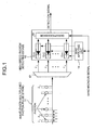
- Fig. 1 is a conceptual diagram of a configuration of a photon detecting device according to a first embodiment of the present invention.
- the photon detecting device shown in Fig. 1 includes a wavelength demultiplexer 12 that distributes photons in a wavelength-multiplexed photon pulse string 11 to different paths depending on wavelength of the photon, a high-speed photon detecting device 13 having plural photon detectors (for example, cooled avalanche photodiodes (APDs)) 13-1 to 13-n, a bias applying unit 14 that sequentially and cyclically applies an inverse bias voltage (a gate pulse) larger than a breakdown voltage V B of the APD to each of the APDs 13-1 to 13-n of the high-speed photon detecting device 13, and a data processor 15 that converts detection signals output from the APDs 13-1 to 13-n of the high-speed photon detector 13 into time series signals (serial signals).
- APDs cooled avalanche photodiodes
- An arrayed-waveguide grating (AWG) demultiplexer for example, can be used for the wavelength demultiplexer 12.
- the AWG demultiplexer includes a planer lightwave circuit (PLC), and it can be integrated on the same substrate as the arrayed APD photon detector. Therefore, the AWG demultiplexer can be made compact, can have a high function, and can be provided at low cost.
- PLC planer lightwave circuit
- the APD photon detectors do not need to be an arrayed type, and the optical fibers of the ports can be individually connected to n APD photon detectors.
- a thin-film filter for example, can also be used for the wavelength demultiplexer 12.
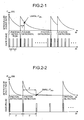
- Figs. 2-1 and Fig. 2-2 are schematic diagrams of a relationship between photon detection, a probability of occurrence of an after-pulse, and a gate pulse string, when the intensity of an incident light is very weak and when photons are detected only sparsely relative to the gate pulse string.
- Fig. 2-1 depicts an example when the time interval T of the gate pulse string is shorter
- Fig. 2-2 depicts an example when the time interval T' of the gate pulse string is longer.
- Fig. 3 depicts a result of an experiment for observing the probability P after (t) of the occurrence of an after-pulse after a predetermined time elapses since the photon detection.
- P after (t) the probability of the occurrence of an after-pulse after a predetermined time elapses since the photon detection.
- Fig. 4 is a schematic diagram of a state of a gate pulse (corresponding to an inverse bias voltage) string applied by the bias applying unit 14 to each of the APDs 13-1 to 13-n of the high-speed photon detecting device 13.
- Fig. 5 depicts a relationship between the voltage V bias of a gate pulse string and an APD current.
- I d denotes a dark current of the APD.
- the bias applying unit 14 applies a gate pulse string to each of the n APDs 13-1 to 13-n in a cycle nT that is n times the time interval T of the wavelength-multiplexed photon pulse string 11 shown in Fig. 1, based on a synchronous signal.
- Each gate pulse (an inverse bias voltage) applied to each of the APDs 13-1 to 13-n by the bias applying unit 14 at the time interval nT changes between a voltage V B + ⁇ V larger than the breakdown voltage V B of the APD and a voltage V B - ⁇ V smaller than the breakdown voltage V B of the APD.
- n APDs 13-1 to 13-n are used, and a gate pulse is applied to the n APDs 13-1 to 13-n at the time interval nT that is n times the time interval T of the wavelength-multiplexed pulse string 11. Therefore, a response speed required for each of the APDs 13-1 to 13-n can be set to 1/n.
- the data processor 15 receives an output of the APDs 13-1 to 13-n of the high-speed photon detecting device 13.
- the data processor 15 performs the data processing of converting photon detection signals output from the APDs 13-1 to 13-n into time series serial signals while holding the time series sequence of the photon detection signals.
- the data processor 15 outputs the data-processed signals as detection signals.
- the wavelength-multiplexed photon pulse string 11 that comes at a constant interval of the constant time interval T is incident to the wavelength demultiplexer 12.
- the wavelength-multiplexed photon pulse string 11 is sufficient when the coming cycle of the pulse string is synchronous with the synchronous signal (the clock signal).
- the light intensity is very weak, a photon does not always need to be included in each pulse string. In other words, photons can come at random in an irregular state so long as the photons come at an interval of an optional integral multiple of time T.
- the wavelength demultiplexer 12 demultiplexes a first incident photon of the wavelength-multiplexed photon pulse string 11 that is incident to the wavelength demultiplexer 12, and inputs the demultiplexed first incident photon to any one of the APDs 13-1 to 13-n (for example, the first APD 13-1) of the high-speed photon detecting device 13.
- a gate pulse an inverse bias voltage
- a signal pulse is generated in the output of one APD to which the first photon is incident, due to the avalanche effect. No signal pulse is generated in the outputs of other APDs to which no photon is incident.
- the next photon is incident to the APD to which the first photon is incident, after the time nT that is n times the time interval T of the wavelength-multiplexed photon pulse string 11 elapses since the incidence of the first photon.
- the signal pulse that is output from the first APD to which the photon is incident is transmitted to the data processor 15.
- a second photon is incident to the wavelength demultiplexer 12.
- the wavelength demultiplexer 12 demultiplexes the second photon, and inputs this demultiplexed second photon to the second APD 13-2, for example. Based on this incidence, a signal pulse is generated in the output of the second APD 13-2, similarly to the above process.
- the signal pulse that is output from the second APD to which the photon is incident is transmitted to the data processor 15.
- a next photon is incident to the APD to which the second photon is incident, after the time nT elapses since the incidence of the second photon.
- the data processor 15 converts the photon detection signals output from the APDs 13-1 to 13-n into time series serial signals, and outputs the time series serial signals.
- the apparent response speed of each photon detection element can be increased.
- the apparent response speed of each photon detection element can be ideally increased by n times.
- the time interval (cycle) of each incident photon in the wavelength-multiplexed photon pulse string 11 is set to T in Fig. 1, it is sufficient if the time interval of the pulse string having the same wavelength is constant, and the time interval of pulses having different wavelengths does not need to be constant. In other words, the pulse strings having different wavelengths are not required to be time division multiplexed.
- the APDs 13-1 to 13-n are provided in the high-speed photon detecting device 13, and the wavelength demultiplexer 12 demultiplexes the wavelength-multiplexed photon pulse string 11 so that the demultiplexed wavelength-multiplexed photon pulse string 11 is distributed to the APDs 13-1 to 13-n. Therefore, the interval of the gate pulse (the inverse bias voltage) applied to each of the APDs 13-1 to 13-n can be the time nT that is n times the time interval T of the wavelength-multiplexed photon pulse string 11.
- the photon detecting device can increase the apparent response speed of each of the photon detection elements (APDs) 13-1 to 13-n by n times. Accordingly, even when a low-speed photon detection element is used a photon can be detected at a high speed.
- APDs photon detection elements
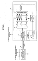
- Fig. 6 is a conceptual diagram of a configuration of an optical communication system according to a second embodiment of the present invention.
- the photon detecting device according to the first embodiment is applied as a quantum cryptographic receiver in the quantum cryptographic communication.
- the optical communication system shown in Fig. 6 includes a quantum cryptographic transmitter 51, and a quantum cryptographic receiver 56.
- the quantum cryptographic transmitter 51 includes a quantum cryptographic modulator 52 that modulates a signal photon following a quantum cryptographic protocol, and a multiplexer (not shown) that multiplexes a clock signal light having higher light intensity than that of a signal photon with the signal photon.
- the quantum cryptographic receiver 56 includes a quantum cryptographic demodulator 54 that demodulates a reception signal received via a transmission path 53, a clock extractor 55 that extracts a clock signal received from the reception signal, and a photon detecting device 20 equivalent to the photon detecting device according to the first embodiment.
- the photon detecting device 20 is similar to that explained in the first embodiment, and includes the wavelength demultiplexer 12, the high-speed photon detecting device 13, the bias applying unit 14, and the data processor 15.
- the signal photon modulated by the quantum cryptographic modulator 52 of the quantum cryptographic transmitter 51 following the quantum cryptographic protocol is multiplexed with the clock signal light.
- the multiplexed result is transmitted through the transmission path 53, and is incident to the quantum cryptographic receiver 56.
- the quantum cryptographic demodulator 54 of the quantum cryptographic receiver 56 demodulates the signal photon incident thereto, and inputs the demodulated signal photon to the wavelength demultiplexer 12.
- the clock signal light that is demultiplexed and separated from the signal photon by the quantum cryptographic demodulator 54 is transmitted to the clock extractor 55.
- the clock extractor 55 extracts the clock signal (the synchronous signal) to take synchronization.
- the synchronous signal extracted by the clock extractor 55 is transmitted to the bias applying unit 14, similarly to the first embodiment.
- the bias applying unit 14 operates similarly to that in the first embodiment.
- the wavelength demultiplexer 12 demultiplexes the signal photon incident thereto, and inputs the demultiplexed signal photon to the high-speed photon detecting device 13 including the photon detection elements 13-1 to 13-n.
- the data processor 15 converts signals detected by the high-speed photon detecting device 13 into time series signals, and outputs the time series signals.
- one set of the photon detecting device 20 can be set in each path.
- the photon detecting device explained in the first embodiment is applied to the quantum cryptographic receiver of the optical communication system. Therefore, a photon can be detected in a single-photon level at a high speed, and a sharing speed of a quantum cryptographic key can be increased.
- the present invention is useful as a photon detecting device that is essential for a quantum cryptographic receiver in a quantum cryptographic communication.
- the present invention is suitable for increasing the detection speed of a photon in a single-photon level.
Landscapes
- Engineering & Computer Science (AREA)
- Physics & Mathematics (AREA)
- Electromagnetism (AREA)
- Computer Networks & Wireless Communication (AREA)
- Signal Processing (AREA)
- Theoretical Computer Science (AREA)
- Computer Security & Cryptography (AREA)
- Optics & Photonics (AREA)
- Optical Communication System (AREA)
- Photometry And Measurement Of Optical Pulse Characteristics (AREA)
- Light Receiving Elements (AREA)
Abstract
Description
- The present invention generally relates to a photon detecting device that is used for quantum information processing such as transfer of a quantum cipher using a single-photon optical source. The invention specifically relates to an optical communication system including a photon detecting device that can detect a photon at a high speed in a single-photon level and the photon detecting device.
- Since a technique of a single-photon detector is essential in the field of quantum information processing such as quantum cryptography and quantum calculation, in addition to high-sensitivity measurement, there is recently a rapidly increasing demand for the single-photon detector. Particularly, a high-speed photon receiver having a high detection efficiency is necessary in the quantum cryptography and quantum communications, to achieve a high-speed communication over a long communication distance, like a general optical communication.
- A photon detector using a cooled avalanche photodiode (APD) and a photo multiplier tube (PMT) is generally used in ultrasensitive optical measurement in which a signal light in a single-photon level is received. Particularly, because the PMT has little sensitivity in a communication waveband of 1.5 micrometers, it is common to use the photon detector using the cooled APD.
- From the viewpoint of sensitivity, an APD of indium, gallium, and arsenic (InGaAs) system is generally used to detect a photon in the 1.5 micrometer band. The
Non-patent Literature 1 discloses an example of a conventional technique concerning the photon detection using the APD of indium, gallium, and arsenic (InGaAs) system. - In technique disclosed in the
Nonpatent Literature 1, the APD used for the photon detection is driven in a specific bias condition called a Geiger operation mode. In the Geiger operation mode, an inverse bias voltage is applied to the APD at a slightly higher level than a breakdown voltage VB of the APD, and in this state, an electron avalanche generated due to the incidence of a photon is measured as a pulse signal. When the incident photon comes cyclically in synchronism with a clock signal, a drive system called a gated Geiger operation mode is used to sequentially and cyclically apply an inverse bias voltage (a gate pulse) larger than the breakdown voltage VB of the APD to match an incidence timing of a signal photon. In other words, when the photon is incident at the moment when the inverse bias voltage becomes larger than the breakdown voltage VB, a signal pulse is generated in an output signal at a constant detection efficiency. When no photon is detected, nothing is output as an output signal. - If such a photon detector is to be used for quantum cryptographic communications, for example, the time interval T of the coming of photons is shortened when there is a need to increase the communication speed. However, a phenomenon called an after-pulse occurs in the photon detector according to the APD that is driven in the gated Geiger operation mode, as described in the
Nonpatent Literature 1. When a gate pulse is applied to the APD in synchronism with the clock signal after the photon detection, an electron avalanche can occur to output an error signal pulse, despite that no photon is incident. The interval of the occurrence of the after-pulse decreases when the time elapsed after the detection of a photon becomes longer. The after-pulse occurs due to a carrier that remains in an element at the time of the last avalanche amplification in the APD. - To eliminate the influence of the after-pulse, the following method and the like are proposed (see, for example, Non-patent Literature 2). For example, when the intensity of an incident light is very weak and when photons are detected only sparsely relative to the cycle of the gate pulse, time for not applying the gate pulse for a constant period of time is provided after the photon detection. The application of the gate pulse is started again after a count rate of the after-pulse becomes sufficiently low.
- However, according to this method, when photons come frequently, longer dead time is generated due to suspension of the application of the gate pulse, whereby the efficiency of detection deteriorates. Therefore, this method is impractical.
-
- Non-patent Literature 1: D. Stucki et al., "Photon counting for quantum key distribution with Peltier cooled InGaAs APDs," J. Mod. Opt. 48, 1967 (2001))
- Non-patent Literature 2: D. Stucki et al., "Quantum key distribution over 67 km with a plug&play system," New J. Phys 4, 41.1-41.8 (2002); A. Yoshizawa et al., "A Method of Discarding After-Pulses in Single-Photon Detection for Quantum Key Distribution," Jpn. J. Appl. Phys. 41, 6016-6017(2002))
- The conventional photon detector has a problem in that the response speed of photon detection cannot be increased to a sufficiently high speed due to the influence of the after-pulse.
- In addition to the above limit to the response time of the photon detector generated due to the influence of the after-pulse, a response speed limit due to an intrinsic element characteristic of the APD also occurs. Generally, the APD has a tradeoff relationship between the response speed and a quantum efficiency. Therefore, a photon detector with a high quantum efficiency has lower response speed.
- Under the above circumstances, it is an object of the present invention to provide a high-speed photon detecting device that can substantially improve an apparent response speed from the response speed of a single-photon detector.
- To solve the above problems, and to achieve the above objects, a photon detecting device includes a wavelength demultiplexer that demultiplexes a wavelength multiplexed incident photon pulse string based on wavelengths of the photons in the photon pulse string; a plurality of photon detectors that detect photons which are demultiplexed by the wavelength demultiplexer; a bias applying unit that applies a gate pulse as a bias voltage to each of the photon detectors to match an incidence timing of an output light of the wavelength demultiplexer to the photon detectors; and a data processor that converts detection signals from the photon detectors into time series signals.
- According to the present invention, a wavelength demultiplexer demultiplexes a wavelength-multiplexed incident photon pulse string for each wavelength, plural photon detectors detect photons that are demultiplexed by the wavelength demultiplexer, a bias applying unit applies a gate pulse as a bias voltage to each of the photon detectors to match the incidence timing of an output light of the wavelength demultiplexer to the photon detectors, and a data processor converts detection signals from the photon detectors into time series signals.
- The photon detecting device according to the present invention can increase the apparent response speed of each of plural photon detection elements. Therefore, the photon detecting device can detect a photon at a high speed, even when low-speed photon detection elements are used.
-
- [Fig 1] Fig. 1 is a conceptual diagram of a configuration of a photon detecting device according to a first embodiment of the present invention;
- [Fig 2-1] Fig. 2-1 is a schematic diagram of a relationship between photon detection, a probability of occurrence of an after-pulse, and a gate pulse string, when a time interval T of the gate pulse string is shorter;
- [Fig 2-2] Fig. 2-2 is a schematic diagram of a relationship between the photon detection, the probability of the occurrence of an after-pulse, and the gate pulse string, when a time interval T' of the gate pulse string is longer;
- [Fig 3] Fig. 3 depicts a result of an experiment of observing a probability Pafter(t) of occurrence of an after-pulse after the a predetermined time elapses since detection of a photon;
- [Fig 4] Fig. 4 is a schematic diagram of a state of a gate pulse (corresponding to an inverse bias voltage) string applied by a
bias applying unit 14 to each of APDs 13-1 to 13-n of a high-speedphoton detecting device 13; - [Fig 5] Fig. 5 depicts a relationship between a voltage Vbias of a gate pulse string and an APD current; and
- [Fig 6] Fig. 6 is a conceptual diagram of a configuration of a quantum cryptographic communication system according to a second embodiment of the present invention.
-
- 11
- Wavelength-multiplexed photon pulse string
- 12
- Wavelength demultiplexer
- 13
- High-speed photon detecting device
- 13-1 to 13-n
- Photon detector (APD)
- 14
- Bias applying unit
- 15
- Data processor
- 20
- Photon detecting device
- 51
- Quantum cryptographic transmitter
- 52
- Quantum cryptographic modulator
- 53
- Transmission path
- 54
- Quantum cryptographic demodulator
- 55
- Clock extractor
- 56
- Quantum cryptographic receiver
- Exemplary embodiments of a photon detecting device and an optical communication system including the photon detecting device according to the present invention will be explained in detail below with reference to the accompanying drawings. Note that the present invention is not limited to the embodiments.
- Fig. 1 is a conceptual diagram of a configuration of a photon detecting device according to a first embodiment of the present invention. The photon detecting device shown in Fig. 1 includes a
wavelength demultiplexer 12 that distributes photons in a wavelength-multiplexedphoton pulse string 11 to different paths depending on wavelength of the photon, a high-speedphoton detecting device 13 having plural photon detectors (for example, cooled avalanche photodiodes (APDs)) 13-1 to 13-n, abias applying unit 14 that sequentially and cyclically applies an inverse bias voltage (a gate pulse) larger than a breakdown voltage VB of the APD to each of the APDs 13-1 to 13-n of the high-speedphoton detecting device 13, and adata processor 15 that converts detection signals output from the APDs 13-1 to 13-n of the high-speed photon detector 13 into time series signals (serial signals). - An arrayed-waveguide grating (AWG) demultiplexer, for example, can be used for the
wavelength demultiplexer 12. The AWG demultiplexer includes a planer lightwave circuit (PLC), and it can be integrated on the same substrate as the arrayed APD photon detector. Therefore, the AWG demultiplexer can be made compact, can have a high function, and can be provided at low cost. When photons are to be taken out with optical fibers from output ports of the AWG demultiplexer, the APD photon detectors do not need to be an arrayed type, and the optical fibers of the ports can be individually connected to n APD photon detectors. - A thin-film filter, for example, can also be used for the
wavelength demultiplexer 12. - Influence of the after-pulse is explained next. Figs. 2-1 and Fig. 2-2 are schematic diagrams of a relationship between photon detection, a probability of occurrence of an after-pulse, and a gate pulse string, when the intensity of an incident light is very weak and when photons are detected only sparsely relative to the gate pulse string. Particularly, Fig. 2-1 depicts an example when the time interval T of the gate pulse string is shorter, and Fig. 2-2 depicts an example when the time interval T' of the gate pulse string is longer.
- In the example shown in Fig. 2-1, after the photon detection, a next gate pulse is applied while the count rate Pafter(Δt) of the after-pulse is large. Therefore, a probability that a detection signal is output by error becomes high although no photon is incident.
- On the other hand, in the example shown in Fig. 2-2, the next gate pulse is applied after sufficient time elapses since the photon detection. Therefore, an erroneous detection signal due to an after-pulse is not generated.
- Fig. 3 depicts a result of an experiment for observing the probability Pafter(t) of the occurrence of an after-pulse after a predetermined time elapses since the photon detection. As is clear with reference to Fig. 3, there is a probability that an after-pulse of about 10-2 occurs even after 0.5 microsecond elapses since the photon detection. Therefore, when the interval of the coming of photons is shortened to increase the communication speed, a probability of the occurrence of an error signal increases. For example, when an APD photon detector having the characteristics shown in Fig. 3 is used, an error of about 1% occurs when T=0.5 microsecond.
- Fig. 4 is a schematic diagram of a state of a gate pulse (corresponding to an inverse bias voltage) string applied by the
bias applying unit 14 to each of the APDs 13-1 to 13-n of the high-speedphoton detecting device 13. Fig. 5 depicts a relationship between the voltage Vbias of a gate pulse string and an APD current. In Fig. 5, Id denotes a dark current of the APD. - As shown in Fig. 4, the
bias applying unit 14 applies a gate pulse string to each of the n APDs 13-1 to 13-n in a cycle nT that is n times the time interval T of the wavelength-multiplexedphoton pulse string 11 shown in Fig. 1, based on a synchronous signal. Each gate pulse (an inverse bias voltage) applied to each of the APDs 13-1 to 13-n by thebias applying unit 14 at the time interval nT changes between a voltage VB+ΔV larger than the breakdown voltage VB of the APD and a voltage VB-ΔV smaller than the breakdown voltage VB of the APD. - As explained above, the n APDs 13-1 to 13-n are used, and a gate pulse is applied to the n APDs 13-1 to 13-n at the time interval nT that is n times the time interval T of the wavelength-multiplexed
pulse string 11. Therefore, a response speed required for each of the APDs 13-1 to 13-n can be set to 1/n. - With reference to Fig. 1 again, the
data processor 15 receives an output of the APDs 13-1 to 13-n of the high-speedphoton detecting device 13. Thedata processor 15 performs the data processing of converting photon detection signals output from the APDs 13-1 to 13-n into time series serial signals while holding the time series sequence of the photon detection signals. Thedata processor 15 outputs the data-processed signals as detection signals. - According to the above configuration, the wavelength-multiplexed
photon pulse string 11 that comes at a constant interval of the constant time interval T is incident to thewavelength demultiplexer 12. The wavelength-multiplexedphoton pulse string 11 is sufficient when the coming cycle of the pulse string is synchronous with the synchronous signal (the clock signal). When the light intensity is very weak, a photon does not always need to be included in each pulse string. In other words, photons can come at random in an irregular state so long as the photons come at an interval of an optional integral multiple of time T. - The
wavelength demultiplexer 12 demultiplexes a first incident photon of the wavelength-multiplexedphoton pulse string 11 that is incident to thewavelength demultiplexer 12, and inputs the demultiplexed first incident photon to any one of the APDs 13-1 to 13-n (for example, the first APD 13-1) of the high-speedphoton detecting device 13. At this incident time, a gate pulse (an inverse bias voltage) is already applied to all the APDs 13-1 to 13-n from thebias applying unit 14. As a result, a signal pulse is generated in the output of one APD to which the first photon is incident, due to the avalanche effect. No signal pulse is generated in the outputs of other APDs to which no photon is incident. - While the incident photon pulse is incident to the
wavelength demultiplexer 12 at the constant time interval T, the next photon is incident to the APD to which the first photon is incident, after the time nT that is n times the time interval T of the wavelength-multiplexedphoton pulse string 11 elapses since the incidence of the first photon. - The signal pulse that is output from the first APD to which the photon is incident is transmitted to the
data processor 15. - When the time T lapses since the incidence of the first photon to the
wavelength demultiplexer 12, a second photon is incident to thewavelength demultiplexer 12. Thewavelength demultiplexer 12 demultiplexes the second photon, and inputs this demultiplexed second photon to the second APD 13-2, for example. Based on this incidence, a signal pulse is generated in the output of the second APD 13-2, similarly to the above process. The signal pulse that is output from the second APD to which the photon is incident is transmitted to thedata processor 15. As described above, a next photon is incident to the APD to which the second photon is incident, after the time nT elapses since the incidence of the second photon. - Each time the incident photon pulse is incident to the
wavelength demultiplexer 12 at the time interval T, the above operation is repeated. Thedata processor 15 converts the photon detection signals output from the APDs 13-1 to 13-n into time series serial signals, and outputs the time series serial signals. - With the above configuration, the apparent response speed of each photon detection element (APD) can be increased. For example, when the n APDs 13-1 to 13-n are disposed in the high-speed
photon detecting device 13, the apparent response speed of each photon detection element can be ideally increased by n times. - While the time interval (cycle) of each incident photon in the wavelength-multiplexed
photon pulse string 11 is set to T in Fig. 1, it is sufficient if the time interval of the pulse string having the same wavelength is constant, and the time interval of pulses having different wavelengths does not need to be constant. In other words, the pulse strings having different wavelengths are not required to be time division multiplexed. - As explained above, according to the photon detecting device of the present embodiment, the APDs 13-1 to 13-n are provided in the high-speed
photon detecting device 13, and thewavelength demultiplexer 12 demultiplexes the wavelength-multiplexedphoton pulse string 11 so that the demultiplexed wavelength-multiplexedphoton pulse string 11 is distributed to the APDs 13-1 to 13-n. Therefore, the interval of the gate pulse (the inverse bias voltage) applied to each of the APDs 13-1 to 13-n can be the time nT that is n times the time interval T of the wavelength-multiplexedphoton pulse string 11. Consequently, the photon detecting device according to the present embodiment can increase the apparent response speed of each of the photon detection elements (APDs) 13-1 to 13-n by n times. Accordingly, even when a low-speed photon detection element is used a photon can be detected at a high speed. - Fig. 6 is a conceptual diagram of a configuration of an optical communication system according to a second embodiment of the present invention. In the optical communication system according to the present embodiment, the photon detecting device according to the first embodiment is applied as a quantum cryptographic receiver in the quantum cryptographic communication.
- The optical communication system shown in Fig. 6 includes a
quantum cryptographic transmitter 51, and aquantum cryptographic receiver 56. Thequantum cryptographic transmitter 51 includes aquantum cryptographic modulator 52 that modulates a signal photon following a quantum cryptographic protocol, and a multiplexer (not shown) that multiplexes a clock signal light having higher light intensity than that of a signal photon with the signal photon. - On the other hand, the
quantum cryptographic receiver 56 includes aquantum cryptographic demodulator 54 that demodulates a reception signal received via atransmission path 53, aclock extractor 55 that extracts a clock signal received from the reception signal, and aphoton detecting device 20 equivalent to the photon detecting device according to the first embodiment. Thephoton detecting device 20 is similar to that explained in the first embodiment, and includes thewavelength demultiplexer 12, the high-speedphoton detecting device 13, thebias applying unit 14, and thedata processor 15. - In the optical communication system using the
quantum cryptographic receiver 56, the signal photon modulated by thequantum cryptographic modulator 52 of thequantum cryptographic transmitter 51 following the quantum cryptographic protocol is multiplexed with the clock signal light. The multiplexed result is transmitted through thetransmission path 53, and is incident to thequantum cryptographic receiver 56. - The
quantum cryptographic demodulator 54 of thequantum cryptographic receiver 56 demodulates the signal photon incident thereto, and inputs the demodulated signal photon to thewavelength demultiplexer 12. On the other hand, the clock signal light that is demultiplexed and separated from the signal photon by thequantum cryptographic demodulator 54 is transmitted to theclock extractor 55. Theclock extractor 55 extracts the clock signal (the synchronous signal) to take synchronization. - The synchronous signal extracted by the
clock extractor 55 is transmitted to thebias applying unit 14, similarly to the first embodiment. Thebias applying unit 14 operates similarly to that in the first embodiment. Thewavelength demultiplexer 12 demultiplexes the signal photon incident thereto, and inputs the demultiplexed signal photon to the high-speedphoton detecting device 13 including the photon detection elements 13-1 to 13-n. Thedata processor 15 converts signals detected by the high-speedphoton detecting device 13 into time series signals, and outputs the time series signals. - When it is necessary to branch the signal photon incident to the
quantum cryptographic receiver 56 to plural paths, one set of thephoton detecting device 20 can be set in each path. - As explained above, in the present embodiment, the photon detecting device explained in the first embodiment is applied to the quantum cryptographic receiver of the optical communication system. Therefore, a photon can be detected in a single-photon level at a high speed, and a sharing speed of a quantum cryptographic key can be increased.
- As described above, the present invention is useful as a photon detecting device that is essential for a quantum cryptographic receiver in a quantum cryptographic communication. Particularly, the present invention is suitable for increasing the detection speed of a photon in a single-photon level.
Claims (7)
- A photon detecting device comprising:a wavelength demultiplexer that demultiplexes a wavelength multiplexed incident photon pulse string based on wavelengths of the photons in the photon pulse string;a plurality of photon detectors that detect photons which are demultiplexed by the wavelength demultiplexer;a bias applying unit that applies a gate pulse as a bias voltage to each of the photon detectors to match an incidence timing of an output light of the wavelength demultiplexer to the photon detectors; anda data processor that converts detection signals from the photon detectors into time series signals.
- The photon detecting device according to claim 1, wherein
the incident photon pulse string is obtained by time division multiplexing so that two or more photons of different wavelengths are not included at the same time (time slot). - The photon detecting device according to claim 1, wherein
the wavelength demultiplexer is an arrayed-waveguide grating (AWG) demultiplexer. - The photon detecting device according to claim 1, wherein
the wavelength demultiplexer is a thin-film filter demultiplexer. - The photon detecting device according to claim 1, wherein
the photon detectors are arrayed APD elements. - An optical communication system including a photon detecting device,
in a quantum cryptographic system including:a quantum cryptographic transmitter that functions as a transmission-side device that performs a quantum cryptographic communication using a light signal; anda quantum cryptographic receiver that functions as a reception-side device that performs the quantum cryptographic communication, whereinthe quantum cryptographic receiver includes:a wavelength demultiplexer that demultiplexes a wavelength multiplexed incident photon pulse string, for each wavelength;a plurality of photon detectors that detect photons which are demultiplexed by the wavelength demultiplexer;a bias applying unit that applies a gate pulse as a bias voltage to each of the photon detectors to match an incidence timing of an output light of the wavelength demultiplexer to the photon detectors; anda data processor that converts detection signals from the photon detectors into time series signals. - The optical communication system according to claim 6, wherein
the incident photon pulse string is obtained by time division multiplexing so that two or more photons of different wavelengths are not included at the same time (time slot).
Applications Claiming Priority (1)
| Application Number | Priority Date | Filing Date | Title |
|---|---|---|---|
| PCT/JP2004/009930 WO2006006231A1 (en) | 2004-07-12 | 2004-07-12 | Photon detecting apparatus and optical communication system |
Publications (3)
| Publication Number | Publication Date |
|---|---|
| EP1783931A1 true EP1783931A1 (en) | 2007-05-09 |
| EP1783931A4 EP1783931A4 (en) | 2007-11-28 |
| EP1783931B1 EP1783931B1 (en) | 2009-02-18 |
Family
ID=35783597
Family Applications (1)
| Application Number | Title | Priority Date | Filing Date |
|---|---|---|---|
| EP04747396A Expired - Lifetime EP1783931B1 (en) | 2004-07-12 | 2004-07-12 | Photon detecting apparatus and optical communication system |
Country Status (4)
| Country | Link |
|---|---|
| US (1) | US20080144823A1 (en) |
| EP (1) | EP1783931B1 (en) |
| JP (1) | JP4695594B2 (en) |
| WO (1) | WO2006006231A1 (en) |
Cited By (1)
| Publication number | Priority date | Publication date | Assignee | Title |
|---|---|---|---|---|
| CN102589721A (en) * | 2011-11-28 | 2012-07-18 | 中国科学院武汉物理与数学研究所 | Method for probing ion clock transition of optical frequency standard based on microprocessor |
Families Citing this family (15)
| Publication number | Priority date | Publication date | Assignee | Title |
|---|---|---|---|---|
| JP4883273B2 (en) * | 2006-01-11 | 2012-02-22 | 日本電気株式会社 | Random number quality management device and management method |
| WO2009110282A1 (en) * | 2008-03-06 | 2009-09-11 | 日本電気株式会社 | Quantum cryptography apparatus, and observational result recording device and method for quantum cryptography apparatus |
| US9002009B2 (en) | 2010-06-15 | 2015-04-07 | Los Alamos National Security, Llc | Quantum key distribution using card, base station and trusted authority |
| US8483394B2 (en) | 2010-06-15 | 2013-07-09 | Los Alamos National Security, Llc | Secure multi-party communication with quantum key distribution managed by trusted authority |
| US9287994B2 (en) | 2011-09-30 | 2016-03-15 | Los Alamos National Security, Llc | Great circle solution to polarization-based quantum communication (QC) in optical fiber |
| US9866379B2 (en) | 2011-09-30 | 2018-01-09 | Los Alamos National Security, Llc | Polarization tracking system for free-space optical communication, including quantum communication |
| CA2882288C (en) | 2012-08-17 | 2020-10-27 | Los Alamos National Security, Llc | Quantum communications system with integrated photonic devices |
| JP5990469B2 (en) * | 2013-01-17 | 2016-09-14 | 日本電信電話株式会社 | Wavelength variable receiver and control method |
| GB2514551A (en) * | 2013-05-28 | 2014-12-03 | Ibm | Fluid-cooled electronic circuit device with cooling fluid conduits having optical transmission medium |
| KR101944167B1 (en) | 2014-02-06 | 2019-01-30 | 노키아 테크놀로지스 오와이 | Reception and generation of light |
| CN104579640A (en) * | 2014-12-24 | 2015-04-29 | 上海理工大学 | Real-time delay tracking device and method of quantum communication system |
| US9787409B1 (en) * | 2015-04-30 | 2017-10-10 | Hrl Laboratories, Llc | High-speed optical quantum communication system based on mode-locked laser pulses |
| JP7075065B2 (en) * | 2018-03-19 | 2022-05-25 | 日本電気株式会社 | Photon detector drive timing adjustment method, device and optical communication system |
| JP2024543819A (en) * | 2021-12-02 | 2024-11-26 | カリフォルニア インスティチュート オブ テクノロジー | Quantum network synchronization system |
| CN116170077B (en) * | 2023-04-24 | 2023-08-29 | 中国科学技术大学 | Quantum and classical laser communication multiplexing receiving device and system |
Family Cites Families (15)
| Publication number | Priority date | Publication date | Assignee | Title |
|---|---|---|---|---|
| JPH062359Y2 (en) * | 1990-08-30 | 1994-01-19 | サンクス株式会社 | Optical communication receiver circuit |
| DE69309496T2 (en) * | 1992-12-24 | 1997-08-07 | British Telecommunications Public Ltd. Co., London | KEY DISTRIBUTION SYSTEM AND METHOD USING QUANTUM CRYPTOGRAPHY |
| WO1995007584A1 (en) * | 1993-09-09 | 1995-03-16 | British Telecommunications Public Limited Company | System and method for quantum cryptography |
| JP3028906B2 (en) * | 1994-01-27 | 2000-04-04 | ケイディディ株式会社 | Soliton optical communication system and optical transmitting device and optical receiving device thereof |
| JP3441169B2 (en) * | 1994-07-06 | 2003-08-25 | 浜松ホトニクス株式会社 | Synchronous signal detector |
| FR2763193B1 (en) * | 1997-05-06 | 1999-06-18 | France Telecom | METHOD AND DEVICE FOR QUANTUM DISTRIBUTION OF ENCRYPTION KEY |
| JP3589604B2 (en) * | 1999-12-16 | 2004-11-17 | 日本電信電話株式会社 | Wavelength multiplexing bidirectional optical transmission method and apparatus |
| JP2003018144A (en) * | 2001-06-29 | 2003-01-17 | Nec Corp | Quantum code multinode network, and method of distributing key on multinode network, and quantum coder |
| JP4619578B2 (en) * | 2001-07-25 | 2011-01-26 | 三菱電機株式会社 | Signal state control device and signal state control method |
| JP3855049B2 (en) * | 2002-03-27 | 2006-12-06 | 独立行政法人産業技術総合研究所 | Single photon detector and its afterpulse elimination method |
| US7272317B2 (en) * | 2002-05-13 | 2007-09-18 | Nippon Telegraph And Telephone Corporation | Optical multiplexing communication system using ultra high speed signal transmission |
| JP4041007B2 (en) * | 2002-05-13 | 2008-01-30 | 日本電信電話株式会社 | Optical multiplex communication method, optical multiplex communication system, optical signal multiplexer, and optical multiplex signal separator |
| US7227955B2 (en) * | 2003-02-07 | 2007-06-05 | Magiq Technologies, Inc. | Single-photon watch dog detector for folded quantum key distribution system |
| JP2004264097A (en) * | 2003-02-28 | 2004-09-24 | Mitsubishi Electric Corp | Photon detector unit |
| US7113598B2 (en) * | 2003-05-14 | 2006-09-26 | Science Research Laboratory, Inc. | Methods and systems for high-data-rate quantum cryptography |
-
2004
- 2004-07-12 JP JP2006527664A patent/JP4695594B2/en not_active Expired - Fee Related
- 2004-07-12 US US11/632,314 patent/US20080144823A1/en not_active Abandoned
- 2004-07-12 WO PCT/JP2004/009930 patent/WO2006006231A1/en not_active Ceased
- 2004-07-12 EP EP04747396A patent/EP1783931B1/en not_active Expired - Lifetime
Cited By (2)
| Publication number | Priority date | Publication date | Assignee | Title |
|---|---|---|---|---|
| CN102589721A (en) * | 2011-11-28 | 2012-07-18 | 中国科学院武汉物理与数学研究所 | Method for probing ion clock transition of optical frequency standard based on microprocessor |
| CN102589721B (en) * | 2011-11-28 | 2013-09-25 | 中国科学院武汉物理与数学研究所 | Method for probing ion clock transition of optical frequency standard based on microprocessor |
Also Published As
| Publication number | Publication date |
|---|---|
| US20080144823A1 (en) | 2008-06-19 |
| WO2006006231A1 (en) | 2006-01-19 |
| JP4695594B2 (en) | 2011-06-08 |
| EP1783931B1 (en) | 2009-02-18 |
| JPWO2006006231A1 (en) | 2008-04-24 |
| EP1783931A4 (en) | 2007-11-28 |
Similar Documents
| Publication | Publication Date | Title |
|---|---|---|
| EP1783931B1 (en) | Photon detecting apparatus and optical communication system | |
| Khalighi et al. | Underwater wireless optical communications using silicon photo-multipliers | |
| Patel et al. | Coexistence of high-bit-rate quantum key distribution and data on optical fiber | |
| US7613396B2 (en) | Multiplexing communication system and crosstalk elimination method | |
| US11329730B2 (en) | Quantum communication system having time to frequency conversion and associated methods | |
| GB2513408A (en) | A photon detector and a photon detection method | |
| WO2013002430A1 (en) | Single photon detector in the near infrared using an ingaas/inp avalanche photodiode operated with a bipolar rectangular gating signal. | |
| WO2023249655A3 (en) | Synchronization system for quantum networks | |
| Fisher et al. | A reconfigurable 14-bit 60GPhoton/s single-photon receiver for visible light communications | |
| CN204886965U (en) | No linear light communication system based on photon counting | |
| Shi et al. | Breakdown flash at telecom wavelengths in InGaAs avalanche photodiodes | |
| Griffiths et al. | High-sensitivity free space optical communications using low size, weight and power hardware | |
| JP2004264097A (en) | Photon detector unit | |
| Hamza et al. | On the suitability of employing silicon photomultipliers for underwater wireless optical communication links | |
| US20050265732A1 (en) | Method and apparatus for receiving frequency modulated signals on an intensity modulated optical carrier | |
| CN111049613A (en) | Time Division Multiplexing (TDM) removing device and method | |
| Plenkin et al. | Comparative analysis of single-photon synchronization algorithms in the quantum key distribution system | |
| US20070258592A1 (en) | Systems and Methods for Multiplexing Qkd Channels | |
| Keeler et al. | Skew and jitter removal using short optical pulses for optical interconnection | |
| US20240080184A1 (en) | Photon detection device, reception device, quantum key distribution system, and method for detecting quantum signal | |
| Borkowski et al. | Real-time burst-mode operation of an integrated SOA-PIN/TIA receiver for 25 Gbit/s/λ and faster T (W) DM-PON | |
| Toliver et al. | Impact of spontaneous anti-Stokes Raman scattering on QKD+ DWDM networking | |
| Zhang et al. | Efficient pulse amplitude modulation for SPAD-based receivers | |
| CN211127821U (en) | Time division multiplexing high-speed QKD system | |
| CN206042012U (en) | Synchronizer of full duplex quantum key distribution system based on same wavelength |
Legal Events
| Date | Code | Title | Description |
|---|---|---|---|
| PUAI | Public reference made under article 153(3) epc to a published international application that has entered the european phase |
Free format text: ORIGINAL CODE: 0009012 |
|
| 17P | Request for examination filed |
Effective date: 20070201 |
|
| AK | Designated contracting states |
Kind code of ref document: A1 Designated state(s): CH FR GB LI |
|
| DAX | Request for extension of the european patent (deleted) | ||
| RBV | Designated contracting states (corrected) |
Designated state(s): CH FR GB LI |
|
| A4 | Supplementary search report drawn up and despatched |
Effective date: 20071031 |
|
| RIC1 | Information provided on ipc code assigned before grant |
Ipc: H04J 14/02 20060101ALI20071022BHEP Ipc: H04L 9/08 20060101ALI20071022BHEP Ipc: H04B 10/30 20060101AFI20071022BHEP |
|
| 17Q | First examination report despatched |
Effective date: 20080204 |
|
| GRAP | Despatch of communication of intention to grant a patent |
Free format text: ORIGINAL CODE: EPIDOSNIGR1 |
|
| GRAS | Grant fee paid |
Free format text: ORIGINAL CODE: EPIDOSNIGR3 |
|
| GRAA | (expected) grant |
Free format text: ORIGINAL CODE: 0009210 |
|
| AK | Designated contracting states |
Kind code of ref document: B1 Designated state(s): CH FR GB LI |
|
| REG | Reference to a national code |
Ref country code: GB Ref legal event code: FG4D |
|
| REG | Reference to a national code |
Ref country code: CH Ref legal event code: EP |
|
| PLBE | No opposition filed within time limit |
Free format text: ORIGINAL CODE: 0009261 |
|
| STAA | Information on the status of an ep patent application or granted ep patent |
Free format text: STATUS: NO OPPOSITION FILED WITHIN TIME LIMIT |
|
| 26N | No opposition filed |
Effective date: 20091119 |
|
| REG | Reference to a national code |
Ref country code: CH Ref legal event code: PL |
|
| PG25 | Lapsed in a contracting state [announced via postgrant information from national office to epo] |
Ref country code: CH Free format text: LAPSE BECAUSE OF NON-PAYMENT OF DUE FEES Effective date: 20090731 Ref country code: LI Free format text: LAPSE BECAUSE OF NON-PAYMENT OF DUE FEES Effective date: 20090731 |
|
| REG | Reference to a national code |
Ref country code: GB Ref legal event code: 746 Effective date: 20110516 |
|
| PGFP | Annual fee paid to national office [announced via postgrant information from national office to epo] |
Ref country code: GB Payment date: 20110706 Year of fee payment: 8 |
|
| PGFP | Annual fee paid to national office [announced via postgrant information from national office to epo] |
Ref country code: FR Payment date: 20120719 Year of fee payment: 9 |
|
| GBPC | Gb: european patent ceased through non-payment of renewal fee |
Effective date: 20120712 |
|
| PG25 | Lapsed in a contracting state [announced via postgrant information from national office to epo] |
Ref country code: GB Free format text: LAPSE BECAUSE OF NON-PAYMENT OF DUE FEES Effective date: 20120712 |
|
| REG | Reference to a national code |
Ref country code: FR Ref legal event code: ST Effective date: 20140331 |
|
| PG25 | Lapsed in a contracting state [announced via postgrant information from national office to epo] |
Ref country code: FR Free format text: LAPSE BECAUSE OF NON-PAYMENT OF DUE FEES Effective date: 20130731 |