EP1783845A1 - Phase change memory having multilayer thermal insulation - Google Patents
Phase change memory having multilayer thermal insulation Download PDFInfo
- Publication number
- EP1783845A1 EP1783845A1 EP06021710A EP06021710A EP1783845A1 EP 1783845 A1 EP1783845 A1 EP 1783845A1 EP 06021710 A EP06021710 A EP 06021710A EP 06021710 A EP06021710 A EP 06021710A EP 1783845 A1 EP1783845 A1 EP 1783845A1
- Authority
- EP
- European Patent Office
- Prior art keywords
- thermal insulation
- electrode
- phase
- layer
- memory cell
- Prior art date
- Legal status (The legal status is an assumption and is not a legal conclusion. Google has not performed a legal analysis and makes no representation as to the accuracy of the status listed.)
- Withdrawn
Links
Images






Classifications
-
- H—ELECTRICITY
- H10—SEMICONDUCTOR DEVICES; ELECTRIC SOLID-STATE DEVICES NOT OTHERWISE PROVIDED FOR
- H10N—ELECTRIC SOLID-STATE DEVICES NOT OTHERWISE PROVIDED FOR
- H10N70/00—Solid-state devices having no potential barriers, and specially adapted for rectifying, amplifying, oscillating or switching
- H10N70/20—Multistable switching devices, e.g. memristors
- H10N70/231—Multistable switching devices, e.g. memristors based on solid-state phase change, e.g. between amorphous and crystalline phases, Ovshinsky effect
-
- G—PHYSICS
- G11—INFORMATION STORAGE
- G11C—STATIC STORES
- G11C7/00—Arrangements for writing information into, or reading information out from, a digital store
- G11C7/04—Arrangements for writing information into, or reading information out from, a digital store with means for avoiding disturbances due to temperature effects
-
- H—ELECTRICITY
- H10—SEMICONDUCTOR DEVICES; ELECTRIC SOLID-STATE DEVICES NOT OTHERWISE PROVIDED FOR
- H10N—ELECTRIC SOLID-STATE DEVICES NOT OTHERWISE PROVIDED FOR
- H10N70/00—Solid-state devices having no potential barriers, and specially adapted for rectifying, amplifying, oscillating or switching
- H10N70/011—Manufacture or treatment of multistable switching devices
- H10N70/061—Shaping switching materials
- H10N70/063—Shaping switching materials by etching of pre-deposited switching material layers, e.g. lithography
-
- H—ELECTRICITY
- H10—SEMICONDUCTOR DEVICES; ELECTRIC SOLID-STATE DEVICES NOT OTHERWISE PROVIDED FOR
- H10N—ELECTRIC SOLID-STATE DEVICES NOT OTHERWISE PROVIDED FOR
- H10N70/00—Solid-state devices having no potential barriers, and specially adapted for rectifying, amplifying, oscillating or switching
- H10N70/011—Manufacture or treatment of multistable switching devices
- H10N70/061—Shaping switching materials
- H10N70/066—Shaping switching materials by filling of openings, e.g. damascene method
-
- H—ELECTRICITY
- H10—SEMICONDUCTOR DEVICES; ELECTRIC SOLID-STATE DEVICES NOT OTHERWISE PROVIDED FOR
- H10N—ELECTRIC SOLID-STATE DEVICES NOT OTHERWISE PROVIDED FOR
- H10N70/00—Solid-state devices having no potential barriers, and specially adapted for rectifying, amplifying, oscillating or switching
- H10N70/801—Constructional details of multistable switching devices
- H10N70/821—Device geometry
- H10N70/823—Device geometry adapted for essentially horizontal current flow, e.g. bridge type devices
-
- H—ELECTRICITY
- H10—SEMICONDUCTOR DEVICES; ELECTRIC SOLID-STATE DEVICES NOT OTHERWISE PROVIDED FOR
- H10N—ELECTRIC SOLID-STATE DEVICES NOT OTHERWISE PROVIDED FOR
- H10N70/00—Solid-state devices having no potential barriers, and specially adapted for rectifying, amplifying, oscillating or switching
- H10N70/801—Constructional details of multistable switching devices
- H10N70/821—Device geometry
- H10N70/826—Device geometry adapted for essentially vertical current flow, e.g. sandwich or pillar type devices
-
- H—ELECTRICITY
- H10—SEMICONDUCTOR DEVICES; ELECTRIC SOLID-STATE DEVICES NOT OTHERWISE PROVIDED FOR
- H10N—ELECTRIC SOLID-STATE DEVICES NOT OTHERWISE PROVIDED FOR
- H10N70/00—Solid-state devices having no potential barriers, and specially adapted for rectifying, amplifying, oscillating or switching
- H10N70/801—Constructional details of multistable switching devices
- H10N70/841—Electrodes
- H10N70/8413—Electrodes adapted for resistive heating
-
- H—ELECTRICITY
- H10—SEMICONDUCTOR DEVICES; ELECTRIC SOLID-STATE DEVICES NOT OTHERWISE PROVIDED FOR
- H10N—ELECTRIC SOLID-STATE DEVICES NOT OTHERWISE PROVIDED FOR
- H10N70/00—Solid-state devices having no potential barriers, and specially adapted for rectifying, amplifying, oscillating or switching
- H10N70/801—Constructional details of multistable switching devices
- H10N70/861—Thermal details
- H10N70/8616—Thermal insulation means
-
- H—ELECTRICITY
- H10—SEMICONDUCTOR DEVICES; ELECTRIC SOLID-STATE DEVICES NOT OTHERWISE PROVIDED FOR
- H10N—ELECTRIC SOLID-STATE DEVICES NOT OTHERWISE PROVIDED FOR
- H10N70/00—Solid-state devices having no potential barriers, and specially adapted for rectifying, amplifying, oscillating or switching
- H10N70/801—Constructional details of multistable switching devices
- H10N70/881—Switching materials
- H10N70/882—Compounds of sulfur, selenium or tellurium, e.g. chalcogenides
- H10N70/8825—Selenides, e.g. GeSe
-
- H—ELECTRICITY
- H10—SEMICONDUCTOR DEVICES; ELECTRIC SOLID-STATE DEVICES NOT OTHERWISE PROVIDED FOR
- H10N—ELECTRIC SOLID-STATE DEVICES NOT OTHERWISE PROVIDED FOR
- H10N70/00—Solid-state devices having no potential barriers, and specially adapted for rectifying, amplifying, oscillating or switching
- H10N70/801—Constructional details of multistable switching devices
- H10N70/881—Switching materials
- H10N70/882—Compounds of sulfur, selenium or tellurium, e.g. chalcogenides
- H10N70/8828—Tellurides, e.g. GeSbTe
-
- H—ELECTRICITY
- H10—SEMICONDUCTOR DEVICES; ELECTRIC SOLID-STATE DEVICES NOT OTHERWISE PROVIDED FOR
- H10N—ELECTRIC SOLID-STATE DEVICES NOT OTHERWISE PROVIDED FOR
- H10N70/00—Solid-state devices having no potential barriers, and specially adapted for rectifying, amplifying, oscillating or switching
- H10N70/801—Constructional details of multistable switching devices
- H10N70/881—Switching materials
- H10N70/884—Switching materials based on at least one element of group IIIA, IVA or VA, e.g. elemental or compound semiconductors
-
- G—PHYSICS
- G11—INFORMATION STORAGE
- G11C—STATIC STORES
- G11C13/00—Digital stores characterised by the use of storage elements not covered by groups G11C11/00, G11C23/00, or G11C25/00
- G11C13/0002—Digital stores characterised by the use of storage elements not covered by groups G11C11/00, G11C23/00, or G11C25/00 using resistive RAM [RRAM] elements
- G11C13/0004—Digital stores characterised by the use of storage elements not covered by groups G11C11/00, G11C23/00, or G11C25/00 using resistive RAM [RRAM] elements comprising amorphous/crystalline phase transition cells
Definitions
- Phase-change memories include phase-change materials that exhibit at least two different states.
- Phase-change material may be used in memory cells to store bits of data.
- the states of phase-change material may be referenced to as amorphous and crystalline states.
- the states may be distinguished because the amorphous state generally exhibits higher resistivity than does the crystalline state.
- the amorphous state involves a more disordered atomic structure, while the crystalline state is an ordered lattice.
- Some phase-change materials exhibit two crystalline states, e.g. a face-centered cubic (FCC) state and a hexagonal closest packing (HCP) state. These two crystalline states have different resistivities and may be used to store bits of data.
- FCC face-centered cubic
- HCP hexagonal closest packing
- Phase change in the phase-change materials may be induced reversibly.
- the memory may change from the amorphous state to the crystalline state, and from the crystalline state to the amorphous state, in response to temperature changes.
- the temperature changes to the phase-change material may be achieved in a variety of ways.
- a laser can be directed to the phase-change material, current may be driven through the phase-change material, or current can be fed through a resistive heater adjacent the phase-change material.
- controllable heating of the phase-change material causes controllable phase change within the phase-change material.
- phase-change memory comprises a memory array having a plurality of memory cells that are made of phase-change material
- the memory may be programmed to store data utilizing the memory states of the phase-change material.
- One way to read and write data in such a phase-change memory device is to control a current and/or a voltage pulse that is applied to the phase-change material.
- the level of current and voltage generally corresponds to the temperature induced within the phase-change material in each memory cell.
- the memory cell includes a first electrode, a second electrode, phase-change material contacting the first electrode and the second electrode, multilayer thermal insulation contacting the phase-change material, and dielectric material contacting the multilayer thermal insulation.
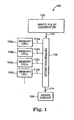
- FIG. 1 illustrates a block diagram of one embodiment of a memory device 100.
- Memory device 100 includes a write pulse generator 102, a distribution circuit 104, memory cells 106a, 106b, 106c, and 106d, and a sense circuit 108.
- memory cells 106a-106d are phase-change memory cells that are based on the amorphous to crystalline phase transition of the memory material.
- Write pulse generator 102 is electrically coupled to distribution circuit 104 through signal path 110.
- Distribution circuit 104 is electrically coupled to memory cells 106a-106d through signal paths 112a-112d, respectively, and to sense circuit 108 through signal path 114.
- Each phase-change memory cell 106a-106d includes phase-change material providing a storage location.
- the phase-change material of each phase-change memory cell 106a-106d is surrounded by multilayer thermal insulation.
- the multilayer thermal insulation provides thermal insulation of the active region of the phase-change material.
- the multilayer thermal insulation laterally surrounds the phase change material.
- the multilayer thermal insulation contacts the phase-change material in the horizontal direction.
- the multilayer thermal insulation relies on a low thermal conductivity of the insulation material layers and also takes advantage of the significant interface resistance for selected insulation material combinations.
- the thermal boundary resistance of ZnS:SiO 2 and GeSbTe can have the same insulating properties as a 5-10nm thick layer of GeSbTe by itself.
- multilayer thermal insulation improves the thermal insulation of the phase-change material and hence lower reset power and reduced structural memory cell size can be achieved.
- the multilayer thermal insulation can also provide some advantages in terms of integration flow by avoiding the use of additional, non-standard materials for complementary metal-oxide-semiconductor (CMOS) processing.
- CMOS complementary metal-oxide-semiconductor
- ZnS:SiO 2 is a typical thermal insulation material widely used in optical DVD applications.
- the integration of ZnS:SiO 2 into CMOS may not be straight forward, since both Zn and S are novel materials, which may need additional diffusion barriers, contamination control, dedicated equipment, etc.
- write pulse generator 102 generates current or voltage pulses that are controllably directed to memory cells 106a-106d via distribution circuit 104.
- distribution circuit 104 includes a plurality of transistors that controllably direct current or voltage pulses to the memory cells.
- memory cells 106a-106d are made of a phase-change material that may be changed from an amorphous state to a crystalline state or from a crystalline state to an amorphous state under influence of temperature change.
- the degree of crystallinity thereby defines at least two memory states for storing data within memory device 100.
- the at least two memory states can be assigned to the bit values "0" and "1".
- the bit states of memory cells 106a-106d differ significantly in their electrical resistivity. In the amorphous state, a phase-change material exhibits significantly higher resistivity than in the crystalline state. In this way, sense amplifier 108 reads the cell resistance such that the bit value assigned to a particular memory cell 106a-106d is determined.
- write pulse generator 102 To program a memory cell 106a-106d within memory device 100, write pulse generator 102 generates a current or voltage pulse for heating the phase-change material in the target memory cell. In one embodiment, write pulse generator 102 generates an appropriate current or voltage pulse, which is fed into distribution circuit 104 and distributed to the appropriate target memory cell 106a-106d. The current or voltage pulse amplitude and duration is controlled depending on whether the memory cell is being set or reset. Generally, a "set” operation of a memory cell is heating the phase-change material of the target memory cell above its crystallization temperature (but below its melting temperature) long enough to achieve the crystalline state. Generally, a "reset” operation of a memory cell is heating the phase-change material of the target memory cell above its melting temperature, and then quickly quench cooling the material, thereby achieving the amorphous state.
- Phase-change memory cell 120a is a pillar phase-change memory cell.
- Phase-change memory cell 120a includes contact plug 122, first electrode 124, phase-change material 126, second electrode 128, thermal insulation material layers 130a, 130b, 130c, and 130d, and dielectric material 132.
- Thermal insulation material layers 130a-130d are collectively referred to as multilayer thermal insulation 130.
- Phase-change material 126 is laterally completely enclosed by thermal insulation material layers 130a-130d.
- thermal insulation material layer 130a is an electric insulator, which defines the current path and hence the location of the phase-change region in phase-change material 126.
- Phase-change material 126 provides a storage location for storing one bit or several bits of data.
- a selection device such as an active device like a transistor or diode, is coupled to contact plug 122 to control the application of current or voltage to first electrode 124, and thus to phase-change material 126, to set and reset phase-change material 126.
- Thermal insulation material layers 130a-130d can comprise a suitable combination of SiO 2 , Al 2 O 3 , AlN, GeSbTe, GeO x , TiO 2 , TiON, TaO x , GeTe, GeN, GaN, GeSb, SiON, SiN, low-k dielectrics, xerogels, aerogels, ZnS-SiO 2 , silica-based porous dielectrics, polymer-based dielectrics, silsesquioxane-based dielectrics, or other suitable thermal insulation material layers.
- multilayer thermal insulation 130 of phase-change memory cell 120a consists of two individual layers, including thermal insulation material layers 130a and 130b.
- thermal insulation material layer 130a includes a material having a lower thermal conductivity than the material of thermal insulation material layer 130b, 130c, or 130d.
- thermal insulation material layer 130a includes an electrically isolating material.
- Thermal insulation material layers 130b-130d include electrically isolating materials, semiconducting materials, or metallic materials. Thermal insulation material layers 130 having a higher thermal conductivity should be thinner than thermal insulation material layers 130 having a lower thermal conductivity, such as less than 5-15nm.
- multilayer thermal insulation 130 it is advantageous to combine material layers having different physical properties, since this will for example decrease the phonon coupling at the interface between the material layers and provide a more pronounced thermal interface resistance.
- a combination could include hard SiO 2 and relatively soft GeSbTe, or a combination could include SiN and porous low-k materials such as silica-based, polymer-based, or silsesquioxane-based low-k materials.
- Phase-change material 126 may be made up of a variety of materials in accordance with the present invention. Generally, chalcogenide alloys that contain one or more elements from group VI of the periodic table are useful as such materials.
- phase-change material 126 of memory cell 120a is made up of a chalcogenide compound material, such as GeSbTe, SbTe, GeTe, or AgInSbTe.
- the phase-change material can be chalcogen free, such as GeSb, GaSb, InSb, or GeGaInSb.
- the phase-change material can be made up of any suitable material including one or more of the elements Ge, Sb, Te, Ga, As, In, Se, and S.
- phase-change memory cell 120a During a set operation of phase-change memory cell 120a, a set current or voltage pulse is selectively enabled to the selection device and sent through contact plug 122 and first electrode 124 to phase-change material 126 thereby heating it above its crystallization temperature (but usually below its melting temperature). In this way, phase-change material 126 reaches its crystalline state during this set operation.
- a reset current or voltage pulse is selectively enabled to the selection device and sent through contact plug 122 and first electrode 124 to phase-change material 126. The reset current or voltage quickly heats phase-change material 126 above its melting temperature. After the current or voltage pulse is turned off, phase-change material 126 quickly quench cools into the amorphous state.
- Phase-change memory cell 120b is a pillar phase-change memory cell.
- Phase-change memory cell 120b is similar to phase-change memory cell 120a, except thermal insulation material layers 130a-130d include angled portions at 134. Whether thermal insulation material layers 130a-130d include the angled portions at 134 (memory cell 120b) or do not include the angled portions (memory cell 120a of Fig. 2) is based on the fabrication process for the phase-change memory cell as described in further detail below.
- Phase-change memory cell 120b operates similarly to phase-change memory cell 120a.
- Phase-change memory cell 120c is an active-in-via phase-change memory cell.
- Phase-change memory cell 120c is similar to phase-change memory cell 120a, except thermal insulation material layers 130a-130d laterally surround phase-change material 126 and second electrode 128, but not first electrode 124.
- First electrode 124 has the same width as contact plug 122.
- first electrode 124 is excluded and contact plug 122 acts as the first electrode.
- thermal insulation material layers 130a-130d include angled portions similar to angled portions 134 illustrated and described with reference to Figure 3. Phase-change memory cell 120c operates similarly to phase-change memory cell 120a.
- FIG. 5-12 illustrate embodiments for fabricating a pillar phase-change memory cell similar to phase-change memory cells 120a and 120b.
- FIG. 5 illustrates a cross-sectional view of one embodiment of a preprocessed wafer 140a.
- Preprocessed wafer 140a includes dielectric material 132, contact plug 122, and lower wafer layers (not shown).
- Contact plug 122 is a tungsten plug, copper plug, or other suitable conducting material plug.
- Dielectric material 132 is SiO 2 , fluorinated silica glass (FSG), doped borophosphorous silicate glass (BPSG), or other suitable dielectric material.
- FIG. 6 illustrates a cross-sectional view of one embodiment of preprocessed wafer 140a, a first electrode material layer 124a, a phase-change material layer 126a, and a second electrode material layer 128a.
- Electrode material such as TiN, TaN, W, Al, Cu, TiSiN, TaSiN, or other suitable electrode material, is deposited over preprocessed wafer 140a to provide first electrode material layer 124a.
- First electrode material layer 124a is deposited using chemical vapor deposition (CVD), atomic layer deposition (ALD), metal organic chemical vapor deposition (MOCVD), plasma vapor deposition (PVD), jet vapor deposition (JVP), or other suitable deposition technique.
- CVD chemical vapor deposition
- ALD atomic layer deposition
- MOCVD metal organic chemical vapor deposition
- PVD plasma vapor deposition
- JVP jet vapor deposition
- Phase-change material such as a chalcogenic compound or other suitable phase-change material, is deposited over first electrode material layer 124a to provide phase-change material layer 126a.
- Phase-change material layer 126a is deposited using CVD, ALD, MOCVD, PVD, JVP, or other suitable deposition technique.
- Electrode material such as TiN, TaN, W, Al, Cu, TiSiN, TaSiN, or other suitable electrode material, is deposited over phase-change material layer 126a to provide second electrode material layer 128a.
- Second electrode material layer 128a is deposited using CVD, ALD, MOCVD, PVD, JVP, or other suitable deposition technique.
- Figure 7 illustrates a cross-sectional view of one embodiment of preprocessed wafer 140a, a first electrode 124, phase-change material 126, and a second electrode 128 after etching second electrode material layer 128a, phase-change material layer 126a, and first electrode material layer 124a.
- Second electrode material layer 128a is etched to provide second electrode 128.
- Phase-change material layer 126a is etched to provide phase-change material 126.
- Phase-change material 126 provides a storage location for storing one bit or several bits of data.
- First electrode material layer 124a is etched to provide first electrode 124. In one embodiment, first electrode 124, phase-change material 126, and second electrode 128 are substantially centered on contact plug 122.
- Figure 8 illustrates a cross-sectional view of one embodiment of preprocessed wafer 140a, first electrode 124, phase-change material 126, second electrode 128, a first thermal insulation material layer 131a, a second thermal insulation material layer 131b, a third thermal insulation material layer 131c, and a fourth thermal insulation material layer 131d.
- Thermal insulation material such as SiO 2 , Al 2 O 3 , AIN, GeN, GaN, SiON, SiN, porous oxide, low-k dielectric, xerogel, aerogel, GeO x , TiO 2 , TiON, TaO x , ZnS-SiO 2 , silica-based porous dielectric, polymer-based dielectric, silsesquioxane-based dielectric, or other suitable electrically isolating thermal insulation material, is deposited over exposed portions of preprocessed wafer 140a, first electrode 124, phase-change material 126, and second electrode 128 to provide first thermal insulation material layer 131a.
- First thermal insulation material layer 131a is deposited using CVD, ALD, MOCVD, PVD, JVP, or other suitable deposition technique.
- Thermal insulation material such as SiO 2 , Al 2 O 3 , AIN, GeSbTe, GeTe, GeN, GaN, GeSb, SiON, SiN, porous oxide, low-k dielectric, xerogel, aerogel, GeO x , TiO 2 , TiON, TaO x , ZnS-SiO 2 , silica-based porous dielectric, polymer-based dielectric, silsesquioxane-based dielectric, or other suitable electrically isolating, semiconducting, or metallic thermal insulation material different than first thermal insulation material layer 131a, is deposited over first thermal insulation material layer 131a to provide second thermal insulation material layer 131b. Second thermal insulation material layer 131b is deposited using CVD, ALD, MOCVD, PVD, JVP, spin-on, or other suitable deposition technique.
- thermal insulation material different than second thermal insulation material layer 131b is deposited over second thermal insulation material layer 131b to provide third thermal insulation material layer 131c.
- Thermal insulation material different than third thermal insulation material layer 131c is deposited over third thermal insulation material layer 131c to provide thermal insulation material layer 131d.
- any suitable number of additional thermal insulation material layers 131 can be deposited over thermal insulation material layer 131d.
- thermal insulation material layers 131c and 131d can be eliminated leaving only thermal insulation material layers 131a and 131b.
- first thermal insulation material layer 131a includes the same material as third thermal insulation material layer 131c
- second thermal insulation material layer 131b includes the same material as fourth thermal insulation material layer 131d
- thermal insulation material layers 131a and 131c include a porous oxide material
- thermal insulation material layers 131b and 131d include a nitride material, such as SiN. In other embodiments, other combinations of materials are possible.
- Figure 9 illustrates a cross-sectional view of one embodiment of preprocessed wafer 140a, first electrode 124, phase-change material 126, second electrode 128, thermal insulation material layers 131a-131d, and dielectric material 132a.
- Dielectric material such as SiO 2 , FSG, BPSG, or other suitable dielectric material, is deposited over fourth thermal insulation material layer 131d to provide dielectric material 132a.
- Dielectric material 132a is deposited using CVD, ALD, MOCVD, PVD, JVP, spin-on, or other suitable deposition technique.
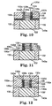
- Figure 10 illustrates a cross-sectional view of one embodiment of preprocessed wafer 140a, first electrode 124, phase-change material 126, second electrode 128, thermal insulation material layers 133a-133d, and dielectric material 132b after planarizing dielectric material 132a and thermal insulation material layers 131a-131d.
- Dielectric material 132a and thermal insulation material layers 131a-131d are planarized to expose second electrode 128.
- Dielectric material 132a and thermal insulation material layers 131a-131d are planarized using chemical mechanical planarization (CMP) or another suitable planarization process to provide phase-change memory cell 120d.
- CMP chemical mechanical planarization
- Phase-change memory cell 120d is similar to phase-change memory cells 120a and 120b, except that the portions of thermal insulation material layers 133a-133d parallel to preprocessed wafer 140a are not etched away. Phase-change memory cell 120d operates similarly to phase-change memory cell 120a.
- Figure 11 illustrates a cross-sectional view of one embodiment of preprocessed wafer 140a, first electrode 124, phase-change material 126, second electrode 128, and thermal insulation material layers 130a-130d after etching thermal insulation material layers 131a-131d in an alternative fabrication process following the fabrication step illustrated and described with reference to Figure 8.
- Thermal insulation material layers 131a-131d are etched to expose preprocessed wafer 140a and second electrode 128 and provide thermal insulation material layers 130a-130d.
- each thermal insulation material layer 131 is deposited and then etched to provide a thermal insulation material layer 130 before the next thermal insulation material layer 131 is deposited.
- the angled portions 134 (Fig. 3) are not formed.
- Figure 12 illustrates a cross-sectional view of one embodiment of preprocessed wafer 140a, first electrode 124, phase-change material 126, second electrode 128, thermal insulation material layers 130a-130d, and dielectric material 132a.
- Dielectric material such as SiO 2 , FSG, BPSG, or other suitable dielectric material, is deposited over exposed portions of preprocessed wafer 140a and insulation material layers 130a-130d.
- Dielectric material 132a is deposited using CVD, ALD, MOCVD, PVD, JVP, or other suitable deposition technique.
- Dielectric material 132a is planarized to exposed second electrode 128.
- Dielectric material 132a is planarized using CMP or another suitable planarization process to provide phase-change memory cell 120b as illustrated in Figure 3.
- FIG. 13-21 illustrate embodiments for fabricating an active-in-via phase-change memory cell similar to phase-change memory cell 120c.
- Figure 13 illustrates a cross-sectional view of one embodiment of a preprocessed wafer 140b.
- Preprocessed wafer 140b includes dielectric material 132, contact plug 122, and lower wafer layers (not shown).
- contact plug 122 is a tungsten plug, copper plug, or other suitable conducting material plug.
- Contact plug 122 provides a first electrode.
- Dielectric material 132 is SiO 2 , FSG, BPSG, or other suitable dielectric material. Dielectric material 132 surrounds the sides and top of contact plug 122.
- Figure 14 illustrates a cross-sectional view of one embodiment of preprocessed wafer 140b after etching.
- Dielectric material 132 is etched to expose contact plug 122 to provide opening 150.
- a portion of contact plug 122 is etched to provide opening 150.
- Figure 15 illustrates a cross-sectional view of one embodiment of preprocessed wafer 140b, a first thermal insulation material layer 152a, a second thermal insulation material layer 152b, a third thermal insulation material layer 152c, and a fourth thermal insulation material layer 152d.
- Thermal insulation material such as SiO 2 , Al 2 O 3 , AIN, GeSbTe, GeTe, GeN, GaN, GeSb, SiON, SiN, porous oxide, or other suitable thermal insulation material, is deposited over preprocessed wafer 140b in opening 150 to provide first thermal insulation material layer 152a.
- First thermal insulation material layer 152a is deposited using CVD, ALD, MOCVD, PVD, JVP, or other suitable deposition technique.
- first thermal insulation material layer 152a is greater than the thickness of each thermal insulation material layer 152b-152d to reduce the cross-section or width of opening 150 to a desired width.
- first insulation material layer 152a includes the same material as dielectric material 132.
- Thermal insulation material such as SiO 2 , Al 2 O 3 , AIN, GeSbTe, GeTe, GeN, GaN, GeSb, SiON, SiN, porous oxide, or other suitable electrically isolating, semiconducting, or metallic thermal insulation material different than first thermal insulation material layer 152a, is deposited over first thermal insulation material layer 152a to provide second thermal insulation material layer 152b.
- Second thermal insulation material layer 152b is deposited using CVD, ALD, MOCVD, PVD, JVP, or other suitable deposition technique.
- thermal insulation material different than second thermal insulation material layer 152b is deposited over second thermal insulation material layer 152b to provide third thermal insulation material layer 152c.
- Thermal insulation material different than third thermal insulation material layer 152c is deposited over third insulation material layer 152c to provide fourth thermal insulation material layer 152d.
- any suitable number of additional thermal insulation material layers 152 can be deposited over thermal insulation material layer 152d.
- thermal insulation material layers 152c and 152d can be eliminated leaving only thermal insulation material layers 152a and 152b.
- thermal insulation material layer 152d, or the last thermal insulation material layer 152 deposited is an electrically isolating material and has the lowest thermal conductivity of the materials used for thermal insulation material layers 152a-152d.
- first thermal insulation material layer 152a includes the same material as third thermal insulation material layer 152c
- second thermal insulation material layer 152b includes the same material as fourth thermal insulation material layer 152d.
- thermal insulation material layers 152a and 152c include a porous oxide material
- thermal insulation material layers 152b and 152d include a nitride material, such as SiN. In other embodiments, other combinations of materials are possible.
- Figure 16 illustrates a cross-sectional view of one embodiment of preprocessed wafer 140b and thermal insulation material layers 154a-154d after etching thermal insulation material layers 152a-152d using a directional reactive ion etch.
- Fourth thermal insulation material layer 152d is etched to provide fourth thermal insulation material layer 154d.
- Third thermal insulation material layer 152c is etched to provide third thermal insulation material layer 154c.
- Second thermal insulation material layer 152b is etched to provide second thermal insulation material layer 154b, and first thermal insulation material layer 152a is etched to provide first thermal insulation material layer 154a.
- Thermal insulation material layers 152a-152d are etched to expose contact plug 122 and dielectric material 132.
- Figure 17 illustrates a cross-sectional view of one embodiment of preprocessed wafer 140b and first thermal insulation material layer 152a.
- Figure 17 illustrates an alternative process for fabricating the phase-change memory cell following the step previously described and illustrated with reference to Figure 14.
- Thermal insulation material such as SiO 2 , Al 2 O 3 , AIN, GeSbTe, GeTe, GeN, GaN, GeSb, SiON, SiN, porous oxide, or other suitable electrically isolating, semiconducting, or metallic thermal insulation material, is deposited over preprocessed wafer 140b to provide first thermal insulation material layer 152a.
- First thermal insulation material layer 152a is deposited using CVD, ALD, MOCVD, PVD, JVP, or other suitable deposition technique.
- the thickness of first thermal insulation material layer 152a is selected to reduce the cross-section or width of opening 150 to a desired sublithographic width.
- first insulation material layer 152a includes the same material as dielectric material 132.
- Figure 18 illustrates a cross-sectional view of one embodiment of preprocessed wafer 140b and first thermal insulation material layer 154a after etching first thermal insulation material layer 152a.
- First insulation material layer 152a is etched to expose contact plug 122 and dielectric material 132 to provide first insulation material layer 154a on the walls of opening 150.
- Figure 19 illustrates a cross-sectional view of one embodiment of preprocessed wafer 140b, first thermal insulation material layer 154a, and a second thermal insulation material layer 152b.
- Thermal insulation material such as SiO 2 , Al 2 O 3 , AIN, GeSbTe, GeTe, GeN, GaN, GeSb, SiON, SiN, porous oxide, or other suitable electrically isolating, semiconducting, or metallic thermal insulation material different than first thermal insulation material layer 154a, is deposited over exposed portions of preprocessed wafer 140b and first thermal insulation material layer 154a to provide second thermal insulation material layer 152b.
- Second thermal insulation material layer 152b is deposited using CVD, ALD, MOCVD, PVD, JVP, or other suitable deposition technique.
- Figure 20 illustrates a cross-sectional view of one embodiment of preprocessed wafer 140b and thermal insulation material layers 154a-154d.
- Second thermal insulation material layer 152b is etched to provide second thermal insulation material layer 154b exposing contact plug 122 and dielectric material 132.
- the steps of depositing and etching a thermal insulation material layer as previously described and illustrated with reference to Figures 18 and 19 are repeated to provide third thermal insulation material layer 154c and fourth thermal insulation material layer 154d.
- any suitable number of additional thermal insulation material layers 152 can be deposited over thermal insulation material layer 154d and etched to provide another thermal insulation material layer 154.
- thermal insulation material layer 154c and/or 154d can be eliminated leaving only thermal insulation material layers 154a and 154b or 154a-154c.
- Thermal insulation material layer 154d, or the last thermal insulation material layer 154 deposited, is an electrically isolating material.
- first thermal insulation material layer 154a includes the same material as third thermal insulation material layer 154c
- second thermal insulation material layer 154b includes the same material as fourth thermal insulation material layer 154d.
- thermal insulation material layers 154a and 154c include a porous oxide material
- thermal insulation material layers 154b and 154d include a nitride material, such as SiN. In other embodiments, other combinations of materials are possible.
- Figure 20 illustrates a similar stage in the phase-change memory cell fabrication process as illustrated in Figure 16. The remaining process steps are the same for both embodiments.
- Figure 21 illustrates a cross-sectional view of one embodiment of a preprocessed wafer 140b, thermal insulation material layers 154a-154d, phase-change material 126, and a second electrode 128.
- Phase-change material such as a chalcogenic compound or other suitable phase-change material, is deposited over contact plug 122 in opening 150 to provide phase-change material 126.
- Phase-change material 126 provides a storage location for storing one bit or several bits of data.
- Phase-change material 126 is deposited using CVD, ALD, MOCVD, PVD, JVP, or other suitable deposition technique.
- Electrode material such as TiN, TaN, W, Al, Cu, TiSiN, TaSiN, or other suitable electrode material, is deposited over phase-change material 126 in opening 150 to provide second electrode 128.
- Second electrode 128 is deposited using CVD, ALD, MOCVD, PVD, JVP, or other suitable deposition technique to provide phase-change memory cell 120e.
- Phase-change memory cell 120e operates similarly to phase-change memory cell 120a.
- Phase-change memory cell 120f is an active-in-via phase-change memory cell.
- Phase-change memory cell 120f is similar to phase-change memory cell 120c, except thermal insulation material layers 130a-130d, phase-change material 126, and second electrode 128 have tapered sidewalls.
- Phase-change memory cell 120f can be fabricated using a process similar to the process previously described and illustrated with reference to Figures 13-21, except that opening 150 is etched with tapered sidewalls.
- Phase-change memory cell 120f operates similarly to phase-change memory cell 120a.
- Phase-change memory cell 120g is an active-in-via phase-change memory cell.
- Phase-change memory cell 120g is similar to phase-change memory cell 120f, except a portion 160 of thermal insulation material layers 130a-130d are substantially parallel to first electrode 124 and a portion 162 of phase-change material 126 is deposited on part of portion 160 of thermal insulation material layers 130a-130d. Portion 164 of thermal insulation material layers 130a-130d and the portion of phase-change material 126 under portion 162 have tapered sidewalls.
- Phase-change memory cell 120g can be fabricated using a process similar to the process previously described and illustrated with reference to Figures 13-21. Phase-change memory cell 120g operates similarly to phase-change memory cell 120a.
- phase-change memory cell 120h is a bridge phase-change memory cell.
- Phase-change memory cell 120h includes contact plug 122, a first contact or electrode 170, phase-change material 126, a second contact or electrode 174, a spacer 172, second electrode 128, thermal insulation material layers 130a-130d, and dielectric material 132.
- Phase-change material 126 provides a storage location for storing one bit, two bits, or several bits of data.
- Phase-change material 126 contacts first contact 170 and second contact 174 separated by spacer 172.
- First contact 170 contacts contact plug 122 and second contact 174 contacts second electrode 128.
- phase-change material 126 is surrounded by thermal insulation material layers 130a-130d.
- thermal insulation material layers 130a-130d include angled portions 134.
- Phase-change memory cell 120h operates similarly to phase-change memory cell 120a.
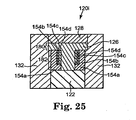
- Phase-change memory cell 120i is an active-in-via phase-change memory cell.
- Phase-change memory cell 120i is similar to phase-change memory cell 120e, except phase-change material 126 extends over the top of thermal insulation material layers 154a-154d and second electrode 128 is surrounded by dielectric material 132.
- Phase-change material 126 includes a first portion 182 contacting contact plug 122 and a second portion 180 contacting second electrode 128.
- First portion 182 of phase-change material 126 is laterally completely enclosed by thermal insulation material layers 154a-154d.
- Second portion 180 of phase-change material 126 is laterally completely enclosed by dielectric material 132.
- Phase-change memory cell 120i can be fabricated using a process similar to the process previously described and illustrated with reference to Figures 13-21. Phase-change memory cell 120i operates similarly to phase-change memory cell 120a.
- Phase-change memory cell 120j is a heater or mushroom phase-change memory cell.
- Phase-change memory cell 120j includes contact plug 122, first electrode or heater 124, phase-change material 126, second electrode 128, thermal insulation material layers 190a, 190b, 190c, and 190d, and dielectric material 132.
- Thermal insulation material layers 190a-190d are collectively referred to as multilayer thermal insulation 190.
- Heater material or first electrode 124 is laterally completely enclosed by thermal insulation material layers 190a-190d, which defines the current path and hence the location of the phase-change region in phase-change material 126.
- Phase-change material 126 provides a storage location for storing one bit or several bits of data.
- a selection device such as an active device like a transistor or diode, is coupled to contact plug 122 to control the application of current or voltage to first electrode or heater 124, and thus to phase-change material 126, to set and reset phase-change material 126.
- Thermal insulation material layers 190a-190d can comprise a suitable combination of SiO 2 , Al 2 O 3 , AIN, GeO x , TiO 2 , TiON, TaO x , GeN, GaN, SiON, SiN, low-k dielectrics, xerogels, aerogels, ZnS-SiO 2 , silica-based porous dielectrics, polymer-based dielectrics, silsesquioxane-based dielectrics, or other suitable thermal insulation material layers.
- multilayer thermal insulation 190 of phase-change memory cell 120j consists of two individual layers, including thermal insulation material layers 190a and 190b, where thermal insulation material layer 190b contacts phase-change material 126.
- thermal insulation material layer 190d includes a material having a lower thermal conductivity than the material of thermal insulation material layer 190a, 190b, or 190c. In one embodiment, thermal insulation material layer 190d includes an electrically isolating material. Thermal insulation material layers 190a-190c include electrically isolating materials, semiconducting materials, or metallic materials. Thermal insulation material layers 190 having a higher thermal conductivity should be thinner than thermal insulation material layers 190 having a lower thermal conductivity, such as less than 5-15nm.
- phase-change memory cell 120j During a set operation of phase-change memory cell 120j, a set current or voltage pulse is selectively enabled to the selection device and sent through contact plug 122 and first electrode or heater 124 to phase-change material 126 thereby heating it above its crystallization temperature (but usually below its melting temperature). In this way, phase-change material 126 reaches its crystalline state during this set operation.
- a reset current or voltage pulse is selectively enabled to the selection device and sent through contact plug 122 and first electrode or heater 124 to phase-change material 126. The reset current or voltage quickly heats phase-change material 126 above its melting temperature. After the current or voltage pulse is turned off, phase-change material 126 quickly quench cools into the amorphous state.
- FIGS. 27-30 illustrate embodiments for fabricating a heater or mushroom phase-change memory cell similar to phase-change memory cell 120j.
- Figure 27 illustrates a cross-sectional view of one embodiment of a preprocessed wafer 140a.
- Preprocessed wafer 140a includes dielectric material 132, contact plug 122, and lower wafer layers (not shown).
- Contact plug 122 is a tungsten plug, copper plug, or other suitable conducting material plug.
- Dielectric material 132 is SiO 2 , FSG, BPSG, or other suitable dielectric material.
- Figure 28 illustrates a cross-sectional view of one embodiment of preprocessed wafer 140a, a first thermal insulation material layer 192a, a second thermal insulation material layer 192b, a third thermal insulation material layer 192c, a fourth thermal insulation material layer 192d, and a sacrificial material layer 132c.
- Thermal insulation material such as SiO 2 , Al 2 O 3 , FSG, BPSG, AIN, GeN, GaN, SiON, SiN, porous oxide, low-k dielectric, xerogel, aerogel, GeO x , TiO 2 , TiON, TaO x , ZnS-SiO 2 , silica-based porous dielectric, polymer-based dielectric, silsesquioxane-based dielectric, or other suitable electrically isolating or semiconducting thermal insulation material, is deposited over preprocessed wafer 140a to provide first thermal insulation material layer 192a.
- First thermal insulation material layer 192a is deposited using CVD, ALD, MOCVD, PVD, JVP, spin-on or other suitable deposition technique.
- Thermal insulation material such as SiO 2 , Al 2 O 3 , FSG, BPSG, AlN, GeN, GaN, SiON, SiN, porous oxide, low-k dielectric, xerogel, aerogel, GeO x , TiO 2 , TiON, TaO x , ZnS-SiO 2 , silica-based porous dielectric, polymer-based dielectric, silsesquioxane-based dielectric, or other suitable electrically isolating or semiconducting thermal insulation material different than first thermal insulation material layer 192a, is deposited over first thermal insulation material layer 192a to provide second thermal insulation material layer 192b. Second thermal insulation material layer 192b is deposited using CVD, ALD, MOCVD, PVD, JVP, spin-on, or other suitable deposition technique.
- thermal insulation material different than second thermal insulation material layer 192b is deposited over second thermal insulation material layer 192b to provide third thermal insulation material layer 192c.
- Thermal insulation material different than third thermal insulation material layer 192c is deposited over third thermal insulation material layer 192c to provide thermal insulation material layer 192d.
- any suitable number of additional thermal insulation material layers 192 can be deposited over thermal insulation material layer 192d.
- thermal insulation material layers 192c and 192d can be eliminated leaving only thermal insulation material layers 192a and 192b.
- first thermal insulation material layer 192a includes the same material as third thermal insulation material layer 192c
- second thermal insulation material layer 192b includes the same material as fourth thermal insulation material layer 192d.
- thermal insulation material layers 192a and 192c include a porous oxide material
- thermal insulation material layers 192b and 192d include a nitride material, such as SiN. In other embodiments, other combinations of materials are possible.
- a sacrificial layer of dielectric material such as SiO 2 , FSG, BPSG, or other suitable dielectric material or conducting material, is deposited over fourth thermal insulation material layer 192d to provide sacrificial material layer 132c.
- Sacrificial material layer 132c is deposited using CVD, ALD, MOCVD, PVD, JVP, spin-on, or other suitable deposition technique.
- Figure 29 illustrates a cross-sectional view of one embodiment of preprocessed wafer 140a, thermal insulation material layers 190a-190d, and sacrificial material layer 132d after etching sacrificial material layer 132c and thermal insulation material layers 192a-192d.
- a via opening 194 is etched into sacrificial material layer 132c to provide sacrificial material layer 132d.
- an additional spacer layer is conformally deposited over via opening 194 and directionally etched back to provide sacrificial material layer 132e exposing a sublithographic portion of thermal insulation material layer 192d.
- the spacer layer includes a suitable dielectric material, semiconducting material, or metallic material.
- the exposed sublithographic portion of thermal insulation material layer 192d and the portions of thermal insulation material layers 192a-192c underneath the exposed portion of thermal insulation material layer 192d are etched to provide thermal insulation material layers 190a-190d.
- Figure 30 illustrates a cross-sectional view of one embodiment of preprocessed wafer 140a, thermal insulation material layers 190a-190d, a first electrode or heater 124, phase-change material 126, and a second electrode 128.
- Dielectric material 132d is stripped.
- Heater or electrode material such as TiN, TaN, W, Al, Cu, TiSiN, TaSiN, or other suitable heater or electrode material, is deposited in via 194 between thermal insulation material layers 190a-190d to provide first electrode or heater 124.
- First electrode or heater 124 is deposited using CVD, ALD, MOCVD, PVD, JVP, or other suitable deposition technique.
- Phase-change material such as a chalcogenic compound or other suitable phase-change material, is deposited over first electrode or heater 124 and thermal insulation material layer 190d to provide a phase-change material layer.
- the phase-change material layer is deposited using CVD, ALD, MOCVD, PVD, JVP, or other suitable deposition technique.
- Electrode material such as TiN, TaN, W, Al, Cu, TiSiN, TaSiN, or other suitable electrode material, is deposited over the phase-change material layer to provide a second electrode material layer.
- the second electrode material layer is deposited using CVD, ALD, MOCVD, PVD, JVP, or other suitable deposition technique.
- the second electrode material layer and the phase-change material layer are etched to provide phase-change material 126 and second electrode 128.
- Dielectric material such as SiO 2 , FSG, BPSG, low-k, or other suitable dielectric material, is deposited around second electrode 128 and phase-change material 126 to provide phase-change memory cell 120j as illustrated in Figure 26.
- Embodiments of the present invention provide a phase-change memory cell having multilayer thermal insulation.
- the multilayer thermal insulation offers improved memory cell insulation and uses typical CMOS materials that are easily integrated into the phase-change memory cell fabrication process.
- the multilayer thermal insulation structure provides increased insulation due to a low bulk thermal conductivity and significant interface resistance for selected material combinations.
- the multilayer thermal insulation allows lower reset power and reduced memory cell size.
Landscapes
- Engineering & Computer Science (AREA)
- Manufacturing & Machinery (AREA)
- Chemical & Material Sciences (AREA)
- Crystallography & Structural Chemistry (AREA)
- Semiconductor Memories (AREA)
Abstract
Description
- Phase-change memories include phase-change materials that exhibit at least two different states. Phase-change material may be used in memory cells to store bits of data. The states of phase-change material may be referenced to as amorphous and crystalline states. The states may be distinguished because the amorphous state generally exhibits higher resistivity than does the crystalline state. Generally, the amorphous state involves a more disordered atomic structure, while the crystalline state is an ordered lattice. Some phase-change materials exhibit two crystalline states, e.g. a face-centered cubic (FCC) state and a hexagonal closest packing (HCP) state. These two crystalline states have different resistivities and may be used to store bits of data. In the following description, the amorphous state generally refers to the state having the higher resistivity, and the crystalline state generally refers to the state having the lower resistivity.
- Phase change in the phase-change materials may be induced reversibly. In this way, the memory may change from the amorphous state to the crystalline state, and from the crystalline state to the amorphous state, in response to temperature changes. The temperature changes to the phase-change material may be achieved in a variety of ways. For example, a laser can be directed to the phase-change material, current may be driven through the phase-change material, or current can be fed through a resistive heater adjacent the phase-change material. With any of these methods, controllable heating of the phase-change material causes controllable phase change within the phase-change material.
- When a phase-change memory comprises a memory array having a plurality of memory cells that are made of phase-change material, the memory may be programmed to store data utilizing the memory states of the phase-change material. One way to read and write data in such a phase-change memory device is to control a current and/or a voltage pulse that is applied to the phase-change material. The level of current and voltage generally corresponds to the temperature induced within the phase-change material in each memory cell.
- One embodiment of the present invention provides a memory cell. The memory cell includes a first electrode, a second electrode, phase-change material contacting the first electrode and the second electrode, multilayer thermal insulation contacting the phase-change material, and dielectric material contacting the multilayer thermal insulation.
- The accompanying drawings are included to provide a further understanding of the present invention and are incorporated in and constitute a part of this specification. The drawings illustrate the embodiments of the present invention and together with the description serve to explain the principles of the invention. Other embodiments of the present invention and many of the intended advantages of the present invention will be readily appreciated as they become better understood by reference to the following detailed description. The elements of the drawings are not necessarily to scale relative to each other. Like reference numerals designate corresponding similar parts.
- Figure 1 illustrates a block diagram of one embodiment of a memory device.
- Figure 2 illustrates a cross-sectional view of one embodiment of a phase-change memory cell.
- Figure 3 illustrates a cross-sectional view of another embodiment of a phase-change memory cell.
- Figure 4 illustrates a cross-sectional view of another embodiment of a phase-change memory cell.
- Figure 5 illustrates a cross-sectional view of one embodiment of a preprocessed wafer.
- Figure 6 illustrates a cross-sectional view of one embodiment of the preprocessed wafer, a first electrode material layer, a phase-change material layer, and a second electrode material layer.
- Figure 7 illustrates a cross-sectional view of one embodiment of the preprocessed wafer, a first electrode, phase-change material, and a second electrode after etching.
- Figure 8 illustrates a cross-sectional view of one embodiment of the preprocessed wafer, first electrode, phase-change material, second electrode, and multilayer thermal insulation.
- Figure 9 illustrates a cross-sectional view of one embodiment of the preprocessed wafer, first electrode, phase-change material, second electrode, multilayer thermal insulation, and a dielectric material.
- Figure 10 illustrates a cross-sectional view of one embodiment of the preprocessed wafer, first electrode, phase-change material, second electrode, multilayer thermal insulation, and dielectric material after planarization.
- Figure 11 illustrates a cross-sectional view of one embodiment of the preprocessed wafer, first electrode, phase-change material, second electrode, and multilayer thermal insulation after etching.
- Figure 12 illustrates a cross-sectional view of one embodiment of the preprocessed wafer, first electrode, phase-change material, second electrode, multilayer thermal insulation, and a dielectric material.
- Figure 13 illustrates a cross-sectional view of another embodiment of a preprocessed wafer.
- Figure 14 illustrates a cross-sectional view of one embodiment of the preprocessed wafer after etching an opening in the preprocessed wafer.
- Figure 15 illustrates a cross-sectional view of one embodiment of the preprocessed wafer and thermal insulation material layers.
- Figure 16 illustrates a cross-sectional view of one embodiment of the preprocessed wafer and thermal insulation material layers after etching.
- Figure 17 illustrates a cross-sectional view of one embodiment the preprocessed wafer and a first thermal insulation material layer.
- Figure 18 illustrates a cross-sectional view of one embodiment of the preprocessed wafer and first thermal insulation material layer after etching.
- Figure 19 illustrates a cross-sectional view of one embodiment of the preprocessed wafer, first thermal insulation material layer, and a second thermal insulation material layer.
- Figure 20 illustrates a cross-sectional view of one embodiment of the preprocessed wafer and thermal insulation material layers after etching.
- Figure 21 illustrates a cross-sectional view of one embodiment of the preprocessed wafer, thermal insulation material layers, phase-change material, and a second electrode.
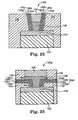
- Figure 22 illustrates a cross-sectional view of another embodiment of a phase-change memory cell.
- Figure 23 illustrates a cross-sectional view of another embodiment of a phase-change memory cell.
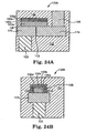
- Figure 24A illustrates a cross-sectional view of another embodiment of a phase-change memory cell.
- Figure 24B illustrates a side cross-sectional view of the embodiment of the phase-change memory cell illustrated in Figure 24A.
- Figure 25 illustrates a cross-sectional view of another embodiment of a phase-change memory cell.
- Figure 26 illustrates a cross-sectional view of another embodiment of a phase-change memory cell.
- Figure 27 illustrates a cross-sectional view of one embodiment of a preprocessed wafer.
- Figure 28 illustrates a cross-sectional view of one embodiment of the preprocessed wafer, thermal insulation material layers, and a sacrificial material layer.
- Figure 29 illustrates a cross-sectional view of one embodiment of the preprocessed wafer, thermal insulation material layers, and sacrificial material layer after etching.
- Figure 30 illustrates a cross-sectional view of one embodiment of the preprocessed wafer, thermal insulation material layers, a first electrode, phase-change material, and a second electrode.
- Figure 1 illustrates a block diagram of one embodiment of a
memory device 100.Memory device 100 includes awrite pulse generator 102, adistribution circuit 104,memory cells sense circuit 108. In one embodiment,memory cells 106a-106d are phase-change memory cells that are based on the amorphous to crystalline phase transition of the memory material.Write pulse generator 102 is electrically coupled todistribution circuit 104 throughsignal path 110.Distribution circuit 104 is electrically coupled tomemory cells 106a-106d throughsignal paths 112a-112d, respectively, and to sensecircuit 108 throughsignal path 114. - Each phase-
change memory cell 106a-106d includes phase-change material providing a storage location. The phase-change material of each phase-change memory cell 106a-106d is surrounded by multilayer thermal insulation. The multilayer thermal insulation provides thermal insulation of the active region of the phase-change material. In memory cell geometries where the current flow through the phase-change material is laterally constricted by an electrical insulator such as in pillar memory cells or pore-type memory cells, the multilayer thermal insulation laterally surrounds the phase change material. In other memory cell geometries where the highest current density is defined by small heater electrode dimensions, the multilayer thermal insulation contacts the phase-change material in the horizontal direction. In one embodiment, the multilayer thermal insulation relies on a low thermal conductivity of the insulation material layers and also takes advantage of the significant interface resistance for selected insulation material combinations. As an example of a possible material combination, the thermal boundary resistance of ZnS:SiO2 and GeSbTe can have the same insulating properties as a 5-10nm thick layer of GeSbTe by itself. - Using multilayer thermal insulation improves the thermal insulation of the phase-change material and hence lower reset power and reduced structural memory cell size can be achieved. In addition, the multilayer thermal insulation can also provide some advantages in terms of integration flow by avoiding the use of additional, non-standard materials for complementary metal-oxide-semiconductor (CMOS) processing. For example, ZnS:SiO2 is a typical thermal insulation material widely used in optical DVD applications. The integration of ZnS:SiO2 into CMOS, however, may not be straight forward, since both Zn and S are novel materials, which may need additional diffusion barriers, contamination control, dedicated equipment, etc.
- In one embodiment, write
pulse generator 102 generates current or voltage pulses that are controllably directed tomemory cells 106a-106d viadistribution circuit 104. In one embodiment,distribution circuit 104 includes a plurality of transistors that controllably direct current or voltage pulses to the memory cells. - In one embodiment,
memory cells 106a-106d are made of a phase-change material that may be changed from an amorphous state to a crystalline state or from a crystalline state to an amorphous state under influence of temperature change. The degree of crystallinity thereby defines at least two memory states for storing data withinmemory device 100. The at least two memory states can be assigned to the bit values "0" and "1". The bit states ofmemory cells 106a-106d differ significantly in their electrical resistivity. In the amorphous state, a phase-change material exhibits significantly higher resistivity than in the crystalline state. In this way,sense amplifier 108 reads the cell resistance such that the bit value assigned to aparticular memory cell 106a-106d is determined. - To program a
memory cell 106a-106d withinmemory device 100, writepulse generator 102 generates a current or voltage pulse for heating the phase-change material in the target memory cell. In one embodiment, writepulse generator 102 generates an appropriate current or voltage pulse, which is fed intodistribution circuit 104 and distributed to the appropriatetarget memory cell 106a-106d. The current or voltage pulse amplitude and duration is controlled depending on whether the memory cell is being set or reset. Generally, a "set" operation of a memory cell is heating the phase-change material of the target memory cell above its crystallization temperature (but below its melting temperature) long enough to achieve the crystalline state. Generally, a "reset" operation of a memory cell is heating the phase-change material of the target memory cell above its melting temperature, and then quickly quench cooling the material, thereby achieving the amorphous state. - Figure 2 illustrates a cross-sectional view of one embodiment of a phase-
change memory cell 120a. In one embodiment, phase-change memory cell 120a is a pillar phase-change memory cell. Phase-change memory cell 120a includescontact plug 122,first electrode 124, phase-change material 126,second electrode 128, thermalinsulation material layers dielectric material 132. Thermalinsulation material layers 130a-130d are collectively referred to as multilayer thermal insulation 130. Phase-change material 126 is laterally completely enclosed by thermalinsulation material layers 130a-130d. In one embodiment, thermalinsulation material layer 130a is an electric insulator, which defines the current path and hence the location of the phase-change region in phase-change material 126. Phase-change material 126 provides a storage location for storing one bit or several bits of data. A selection device, such as an active device like a transistor or diode, is coupled to contactplug 122 to control the application of current or voltage tofirst electrode 124, and thus to phase-change material 126, to set and reset phase-change material 126. - Thermal
insulation material layers 130a-130d can comprise a suitable combination of SiO2, Al2O3, AlN, GeSbTe, GeOx, TiO2, TiON, TaOx, GeTe, GeN, GaN, GeSb, SiON, SiN, low-k dielectrics, xerogels, aerogels, ZnS-SiO2, silica-based porous dielectrics, polymer-based dielectrics, silsesquioxane-based dielectrics, or other suitable thermal insulation material layers. In one embodiment, multilayer thermal insulation 130 of phase-change memory cell 120a consists of two individual layers, including thermalinsulation material layers insulation material layer 130a includes a material having a lower thermal conductivity than the material of thermalinsulation material layer insulation material layer 130a includes an electrically isolating material. Thermal insulation material layers 130b-130d include electrically isolating materials, semiconducting materials, or metallic materials. Thermal insulation material layers 130 having a higher thermal conductivity should be thinner than thermal insulation material layers 130 having a lower thermal conductivity, such as less than 5-15nm. - To form multilayer thermal insulation 130, it is advantageous to combine material layers having different physical properties, since this will for example decrease the phonon coupling at the interface between the material layers and provide a more pronounced thermal interface resistance. For example, a combination could include hard SiO2 and relatively soft GeSbTe, or a combination could include SiN and porous low-k materials such as silica-based, polymer-based, or silsesquioxane-based low-k materials.
- Phase-
change material 126 may be made up of a variety of materials in accordance with the present invention. Generally, chalcogenide alloys that contain one or more elements from group VI of the periodic table are useful as such materials. In one embodiment, phase-change material 126 ofmemory cell 120a is made up of a chalcogenide compound material, such as GeSbTe, SbTe, GeTe, or AgInSbTe. In another embodiment, the phase-change material can be chalcogen free, such as GeSb, GaSb, InSb, or GeGaInSb. In other embodiments, the phase-change material can be made up of any suitable material including one or more of the elements Ge, Sb, Te, Ga, As, In, Se, and S. - During a set operation of phase-
change memory cell 120a, a set current or voltage pulse is selectively enabled to the selection device and sent throughcontact plug 122 andfirst electrode 124 to phase-change material 126 thereby heating it above its crystallization temperature (but usually below its melting temperature). In this way, phase-change material 126 reaches its crystalline state during this set operation. During a reset operation of phase-change memory cell 120a, a reset current or voltage pulse is selectively enabled to the selection device and sent throughcontact plug 122 andfirst electrode 124 to phase-change material 126. The reset current or voltage quickly heats phase-change material 126 above its melting temperature. After the current or voltage pulse is turned off, phase-change material 126 quickly quench cools into the amorphous state. - Figure 3 illustrates a cross-sectional view of another embodiment of a phase-
change memory cell 120b. In one embodiment, phase-change memory cell 120b is a pillar phase-change memory cell. Phase-change memory cell 120b is similar to phase-change memory cell 120a, except thermalinsulation material layers 130a-130d include angled portions at 134. Whether thermalinsulation material layers 130a-130d include the angled portions at 134 (memory cell 120b) or do not include the angled portions (memory cell 120a of Fig. 2) is based on the fabrication process for the phase-change memory cell as described in further detail below. Phase-change memory cell 120b operates similarly to phase-change memory cell 120a. - Figure 4 illustrates a cross-sectional view of another embodiment of a phase-
change memory cell 120c. In one embodiment, phase-change memory cell 120c is an active-in-via phase-change memory cell. Phase-change memory cell 120c is similar to phase-change memory cell 120a, except thermalinsulation material layers 130a-130d laterally surround phase-change material 126 andsecond electrode 128, but notfirst electrode 124.First electrode 124 has the same width ascontact plug 122. In another embodiment,first electrode 124 is excluded and contact plug 122 acts as the first electrode. In another embodiment, thermalinsulation material layers 130a-130d include angled portions similar toangled portions 134 illustrated and described with reference to Figure 3. Phase-change memory cell 120c operates similarly to phase-change memory cell 120a. - The following Figures 5-12 illustrate embodiments for fabricating a pillar phase-change memory cell similar to phase-
change memory cells - Figure 5 illustrates a cross-sectional view of one embodiment of a preprocessed
wafer 140a.Preprocessed wafer 140a includesdielectric material 132,contact plug 122, and lower wafer layers (not shown).Contact plug 122 is a tungsten plug, copper plug, or other suitable conducting material plug.Dielectric material 132 is SiO2, fluorinated silica glass (FSG), doped borophosphorous silicate glass (BPSG), or other suitable dielectric material. - Figure 6 illustrates a cross-sectional view of one embodiment of preprocessed
wafer 140a, a firstelectrode material layer 124a, a phase-change material layer 126a, and a secondelectrode material layer 128a. Electrode material, such as TiN, TaN, W, Al, Cu, TiSiN, TaSiN, or other suitable electrode material, is deposited over preprocessedwafer 140a to provide firstelectrode material layer 124a. Firstelectrode material layer 124a is deposited using chemical vapor deposition (CVD), atomic layer deposition (ALD), metal organic chemical vapor deposition (MOCVD), plasma vapor deposition (PVD), jet vapor deposition (JVP), or other suitable deposition technique. - Phase-change material, such as a chalcogenic compound or other suitable phase-change material, is deposited over first
electrode material layer 124a to provide phase-change material layer 126a. Phase-change material layer 126a is deposited using CVD, ALD, MOCVD, PVD, JVP, or other suitable deposition technique. - Electrode material, such as TiN, TaN, W, Al, Cu, TiSiN, TaSiN, or other suitable electrode material, is deposited over phase-
change material layer 126a to provide secondelectrode material layer 128a. Secondelectrode material layer 128a is deposited using CVD, ALD, MOCVD, PVD, JVP, or other suitable deposition technique. - Figure 7 illustrates a cross-sectional view of one embodiment of preprocessed
wafer 140a, afirst electrode 124, phase-change material 126, and asecond electrode 128 after etching secondelectrode material layer 128a, phase-change material layer 126a, and firstelectrode material layer 124a. Secondelectrode material layer 128a is etched to providesecond electrode 128. Phase-change material layer 126a is etched to provide phase-change material 126. Phase-change material 126 provides a storage location for storing one bit or several bits of data. Firstelectrode material layer 124a is etched to providefirst electrode 124. In one embodiment,first electrode 124, phase-change material 126, andsecond electrode 128 are substantially centered oncontact plug 122. - Figure 8 illustrates a cross-sectional view of one embodiment of preprocessed
wafer 140a,first electrode 124, phase-change material 126,second electrode 128, a first thermalinsulation material layer 131a, a second thermalinsulation material layer 131b, a third thermalinsulation material layer 131c, and a fourth thermalinsulation material layer 131d. Thermal insulation material, such as SiO2, Al2O3, AIN, GeN, GaN, SiON, SiN, porous oxide, low-k dielectric, xerogel, aerogel, GeOx, TiO2, TiON, TaOx, ZnS-SiO2, silica-based porous dielectric, polymer-based dielectric, silsesquioxane-based dielectric, or other suitable electrically isolating thermal insulation material, is deposited over exposed portions of preprocessedwafer 140a,first electrode 124, phase-change material 126, andsecond electrode 128 to provide first thermalinsulation material layer 131a. First thermalinsulation material layer 131a is deposited using CVD, ALD, MOCVD, PVD, JVP, or other suitable deposition technique. - Thermal insulation material, such as SiO2, Al2O3, AIN, GeSbTe, GeTe, GeN, GaN, GeSb, SiON, SiN, porous oxide, low-k dielectric, xerogel, aerogel, GeOx, TiO2, TiON, TaOx, ZnS-SiO2, silica-based porous dielectric, polymer-based dielectric, silsesquioxane-based dielectric, or other suitable electrically isolating, semiconducting, or metallic thermal insulation material different than first thermal
insulation material layer 131a, is deposited over first thermalinsulation material layer 131a to provide second thermalinsulation material layer 131b. Second thermalinsulation material layer 131b is deposited using CVD, ALD, MOCVD, PVD, JVP, spin-on, or other suitable deposition technique. - Likewise, thermal insulation material different than second thermal
insulation material layer 131b is deposited over second thermalinsulation material layer 131b to provide third thermalinsulation material layer 131c. Thermal insulation material different than third thermalinsulation material layer 131c is deposited over third thermalinsulation material layer 131c to provide thermalinsulation material layer 131d. In other embodiments, any suitable number of additional thermal insulation material layers 131 can be deposited over thermalinsulation material layer 131d. In other embodiments, thermal insulation material layers 131c and 131d can be eliminated leaving only thermalinsulation material layers - In one embodiment, first thermal
insulation material layer 131a includes the same material as third thermalinsulation material layer 131c, and second thermalinsulation material layer 131b includes the same material as fourth thermalinsulation material layer 131d. In one embodiment, thermalinsulation material layers - Figure 9 illustrates a cross-sectional view of one embodiment of preprocessed
wafer 140a,first electrode 124, phase-change material 126,second electrode 128, thermalinsulation material layers 131a-131d, anddielectric material 132a. Dielectric material, such as SiO2, FSG, BPSG, or other suitable dielectric material, is deposited over fourth thermalinsulation material layer 131d to providedielectric material 132a.Dielectric material 132a is deposited using CVD, ALD, MOCVD, PVD, JVP, spin-on, or other suitable deposition technique. - Figure 10 illustrates a cross-sectional view of one embodiment of preprocessed
wafer 140a,first electrode 124, phase-change material 126,second electrode 128, thermalinsulation material layers 133a-133d, anddielectric material 132b after planarizingdielectric material 132a and thermalinsulation material layers 131a-131d.Dielectric material 132a and thermalinsulation material layers 131a-131d are planarized to exposesecond electrode 128.Dielectric material 132a and thermalinsulation material layers 131a-131d are planarized using chemical mechanical planarization (CMP) or another suitable planarization process to provide phase-change memory cell 120d. Phase-change memory cell 120d is similar to phase-change memory cells insulation material layers 133a-133d parallel to preprocessedwafer 140a are not etched away. Phase-change memory cell 120d operates similarly to phase-change memory cell 120a. - Figure 11 illustrates a cross-sectional view of one embodiment of preprocessed
wafer 140a,first electrode 124, phase-change material 126,second electrode 128, and thermalinsulation material layers 130a-130d after etching thermalinsulation material layers 131a-131d in an alternative fabrication process following the fabrication step illustrated and described with reference to Figure 8. Thermalinsulation material layers 131a-131d are etched to expose preprocessedwafer 140a andsecond electrode 128 and provide thermalinsulation material layers 130a-130d. - In another embodiment, each thermal insulation material layer 131 is deposited and then etched to provide a thermal insulation material layer 130 before the next thermal insulation material layer 131 is deposited. In this embodiment, the angled portions 134 (Fig. 3) are not formed.
- Figure 12 illustrates a cross-sectional view of one embodiment of preprocessed
wafer 140a,first electrode 124, phase-change material 126,second electrode 128, thermalinsulation material layers 130a-130d, anddielectric material 132a. Dielectric material, such as SiO2, FSG, BPSG, or other suitable dielectric material, is deposited over exposed portions of preprocessedwafer 140a andinsulation material layers 130a-130d.Dielectric material 132a is deposited using CVD, ALD, MOCVD, PVD, JVP, or other suitable deposition technique.Dielectric material 132a is planarized to exposedsecond electrode 128.Dielectric material 132a is planarized using CMP or another suitable planarization process to provide phase-change memory cell 120b as illustrated in Figure 3. - The following Figures 13-21 illustrate embodiments for fabricating an active-in-via phase-change memory cell similar to phase-
change memory cell 120c. - Figure 13 illustrates a cross-sectional view of one embodiment of a preprocessed
wafer 140b.Preprocessed wafer 140b includesdielectric material 132,contact plug 122, and lower wafer layers (not shown). In one embodiment,contact plug 122 is a tungsten plug, copper plug, or other suitable conducting material plug.Contact plug 122 provides a first electrode.Dielectric material 132 is SiO2, FSG, BPSG, or other suitable dielectric material.Dielectric material 132 surrounds the sides and top ofcontact plug 122. - Figure 14 illustrates a cross-sectional view of one embodiment of preprocessed
wafer 140b after etching.Dielectric material 132 is etched to exposecontact plug 122 to provideopening 150. In another embodiment, a portion ofcontact plug 122 is etched to provideopening 150. - Figure 15 illustrates a cross-sectional view of one embodiment of preprocessed
wafer 140b, a first thermalinsulation material layer 152a, a second thermalinsulation material layer 152b, a third thermalinsulation material layer 152c, and a fourth thermalinsulation material layer 152d. Thermal insulation material, such as SiO2, Al2O3, AIN, GeSbTe, GeTe, GeN, GaN, GeSb, SiON, SiN, porous oxide, or other suitable thermal insulation material, is deposited over preprocessedwafer 140b in opening 150 to provide first thermalinsulation material layer 152a. First thermalinsulation material layer 152a is deposited using CVD, ALD, MOCVD, PVD, JVP, or other suitable deposition technique. In one embodiment, the thickness of first thermalinsulation material layer 152a is greater than the thickness of each thermalinsulation material layer 152b-152d to reduce the cross-section or width ofopening 150 to a desired width. In one embodiment, firstinsulation material layer 152a includes the same material asdielectric material 132. - Thermal insulation material, such as SiO2, Al2O3, AIN, GeSbTe, GeTe, GeN, GaN, GeSb, SiON, SiN, porous oxide, or other suitable electrically isolating, semiconducting, or metallic thermal insulation material different than first thermal
insulation material layer 152a, is deposited over first thermalinsulation material layer 152a to provide second thermalinsulation material layer 152b. Second thermalinsulation material layer 152b is deposited using CVD, ALD, MOCVD, PVD, JVP, or other suitable deposition technique. - Likewise, thermal insulation material different than second thermal
insulation material layer 152b is deposited over second thermalinsulation material layer 152b to provide third thermalinsulation material layer 152c. Thermal insulation material different than third thermalinsulation material layer 152c is deposited over thirdinsulation material layer 152c to provide fourth thermalinsulation material layer 152d. In other embodiments, any suitable number of additional thermal insulation material layers 152 can be deposited over thermalinsulation material layer 152d. In other embodiments, thermal insulation material layers 152c and 152d can be eliminated leaving only thermalinsulation material layers insulation material layer 152d, or the last thermal insulation material layer 152 deposited, is an electrically isolating material and has the lowest thermal conductivity of the materials used for thermalinsulation material layers 152a-152d. - In one embodiment, first thermal
insulation material layer 152a includes the same material as third thermalinsulation material layer 152c, and second thermalinsulation material layer 152b includes the same material as fourth thermalinsulation material layer 152d. In one embodiment, thermalinsulation material layers - Figure 16 illustrates a cross-sectional view of one embodiment of preprocessed
wafer 140b and thermalinsulation material layers 154a-154d after etching thermalinsulation material layers 152a-152d using a directional reactive ion etch. Fourth thermalinsulation material layer 152d is etched to provide fourth thermalinsulation material layer 154d. Third thermalinsulation material layer 152c is etched to provide third thermalinsulation material layer 154c. Second thermalinsulation material layer 152b is etched to provide second thermalinsulation material layer 154b, and first thermalinsulation material layer 152a is etched to provide first thermalinsulation material layer 154a. Thermalinsulation material layers 152a-152d are etched to exposecontact plug 122 anddielectric material 132. - Figure 17 illustrates a cross-sectional view of one embodiment of preprocessed
wafer 140b and first thermalinsulation material layer 152a. Figure 17 illustrates an alternative process for fabricating the phase-change memory cell following the step previously described and illustrated with reference to Figure 14. Thermal insulation material, such as SiO2, Al2O3, AIN, GeSbTe, GeTe, GeN, GaN, GeSb, SiON, SiN, porous oxide, or other suitable electrically isolating, semiconducting, or metallic thermal insulation material, is deposited over preprocessedwafer 140b to provide first thermalinsulation material layer 152a. First thermalinsulation material layer 152a is deposited using CVD, ALD, MOCVD, PVD, JVP, or other suitable deposition technique. In one embodiment, the thickness of first thermalinsulation material layer 152a is selected to reduce the cross-section or width ofopening 150 to a desired sublithographic width. In one embodiment, firstinsulation material layer 152a includes the same material asdielectric material 132. - Figure 18 illustrates a cross-sectional view of one embodiment of preprocessed
wafer 140b and first thermalinsulation material layer 154a after etching first thermalinsulation material layer 152a. Firstinsulation material layer 152a is etched to exposecontact plug 122 anddielectric material 132 to provide firstinsulation material layer 154a on the walls ofopening 150. - Figure 19 illustrates a cross-sectional view of one embodiment of preprocessed
wafer 140b, first thermalinsulation material layer 154a, and a second thermalinsulation material layer 152b. Thermal insulation material, such as SiO2, Al2O3, AIN, GeSbTe, GeTe, GeN, GaN, GeSb, SiON, SiN, porous oxide, or other suitable electrically isolating, semiconducting, or metallic thermal insulation material different than first thermalinsulation material layer 154a, is deposited over exposed portions of preprocessedwafer 140b and first thermalinsulation material layer 154a to provide second thermalinsulation material layer 152b. Second thermalinsulation material layer 152b is deposited using CVD, ALD, MOCVD, PVD, JVP, or other suitable deposition technique. - Figure 20 illustrates a cross-sectional view of one embodiment of preprocessed
wafer 140b and thermalinsulation material layers 154a-154d. Second thermalinsulation material layer 152b is etched to provide second thermalinsulation material layer 154b exposingcontact plug 122 anddielectric material 132. The steps of depositing and etching a thermal insulation material layer as previously described and illustrated with reference to Figures 18 and 19 are repeated to provide third thermalinsulation material layer 154c and fourth thermalinsulation material layer 154d. In other embodiments, any suitable number of additional thermal insulation material layers 152 can be deposited over thermalinsulation material layer 154d and etched to provide another thermal insulation material layer 154. In other embodiments, thermalinsulation material layer 154c and/or 154d can be eliminated leaving only thermalinsulation material layers insulation material layer 154d, or the last thermal insulation material layer 154 deposited, is an electrically isolating material. - In one embodiment, first thermal
insulation material layer 154a includes the same material as third thermalinsulation material layer 154c, and second thermalinsulation material layer 154b includes the same material as fourth thermalinsulation material layer 154d. In one embodiment, thermalinsulation material layers - Figure 21 illustrates a cross-sectional view of one embodiment of a preprocessed
wafer 140b, thermalinsulation material layers 154a-154d, phase-change material 126, and asecond electrode 128. Phase-change material, such as a chalcogenic compound or other suitable phase-change material, is deposited overcontact plug 122 in opening 150 to provide phase-change material 126. Phase-change material 126 provides a storage location for storing one bit or several bits of data. Phase-change material 126 is deposited using CVD, ALD, MOCVD, PVD, JVP, or other suitable deposition technique. - Electrode material, such as TiN, TaN, W, Al, Cu, TiSiN, TaSiN, or other suitable electrode material, is deposited over phase-
change material 126 in opening 150 to providesecond electrode 128.Second electrode 128 is deposited using CVD, ALD, MOCVD, PVD, JVP, or other suitable deposition technique to provide phase-change memory cell 120e. Phase-change memory cell 120e operates similarly to phase-change memory cell 120a. - Figure 22 illustrates a cross-sectional view of another embodiment of a phase-
change memory cell 120f. In one embodiment, phase-change memory cell 120f is an active-in-via phase-change memory cell. Phase-change memory cell 120f is similar to phase-change memory cell 120c, except thermalinsulation material layers 130a-130d, phase-change material 126, andsecond electrode 128 have tapered sidewalls. Phase-change memory cell 120f can be fabricated using a process similar to the process previously described and illustrated with reference to Figures 13-21, except thatopening 150 is etched with tapered sidewalls. Phase-change memory cell 120f operates similarly to phase-change memory cell 120a. - Figure 23 illustrates a cross-sectional view of another embodiment of a phase-
change memory cell 120g. In one embodiment, phase-change memory cell 120g is an active-in-via phase-change memory cell. Phase-change memory cell 120g is similar to phase-change memory cell 120f, except aportion 160 of thermalinsulation material layers 130a-130d are substantially parallel tofirst electrode 124 and aportion 162 of phase-change material 126 is deposited on part ofportion 160 of thermalinsulation material layers 130a-130d.Portion 164 of thermalinsulation material layers 130a-130d and the portion of phase-change material 126 underportion 162 have tapered sidewalls. Phase-change memory cell 120g can be fabricated using a process similar to the process previously described and illustrated with reference to Figures 13-21. Phase-change memory cell 120g operates similarly to phase-change memory cell 120a. - Figure 24A illustrates a cross-sectional view of another embodiment of a phase-
change memory cell 120h, and Figure 24B illustrates a side cross-sectional view of phase-change memory cell 120h. In one embodiment, phase-change memory cell 120h is a bridge phase-change memory cell. Phase-change memory cell 120h includescontact plug 122, a first contact orelectrode 170, phase-change material 126, a second contact orelectrode 174, aspacer 172,second electrode 128, thermalinsulation material layers 130a-130d, anddielectric material 132. Phase-change material 126 provides a storage location for storing one bit, two bits, or several bits of data. - Phase-
change material 126 contactsfirst contact 170 andsecond contact 174 separated byspacer 172. First contact 170contacts contact plug 122 andsecond contact 174 contactssecond electrode 128. Except for the phase-changematerial contacting contacts spacer 172, phase-change material 126 is surrounded by thermalinsulation material layers 130a-130d. In one embodiment, thermalinsulation material layers 130a-130d includeangled portions 134. Phase-change memory cell 120h operates similarly to phase-change memory cell 120a. - Figure 25 illustrates a cross-sectional view of another embodiment of a phase-
change memory cell 120i. In one embodiment, phase-change memory cell 120i is an active-in-via phase-change memory cell. Phase-change memory cell 120i is similar to phase-change memory cell 120e, except phase-change material 126 extends over the top of thermalinsulation material layers 154a-154d andsecond electrode 128 is surrounded bydielectric material 132. Phase-change material 126 includes afirst portion 182 contactingcontact plug 122 and a second portion 180 contactingsecond electrode 128.First portion 182 of phase-change material 126 is laterally completely enclosed by thermalinsulation material layers 154a-154d. Second portion 180 of phase-change material 126 is laterally completely enclosed bydielectric material 132.First portion 182 and second portion 180 of phase-change material 126 completely enclose the open ends of thermalinsulation material layers 154a-154d preventing thermal conduction to contactplug 122 andsecond electrode 128. Phase-change memory cell 120i can be fabricated using a process similar to the process previously described and illustrated with reference to Figures 13-21. Phase-change memory cell 120i operates similarly to phase-change memory cell 120a. - Figure 26 illustrates a cross-sectional view of another embodiment of a phase-
change memory cell 120j. In one embodiment, phase-change memory cell 120j is a heater or mushroom phase-change memory cell. Phase-change memory cell 120j includescontact plug 122, first electrode orheater 124, phase-change material 126,second electrode 128, thermalinsulation material layers dielectric material 132. Thermalinsulation material layers 190a-190d are collectively referred to as multilayer thermal insulation 190. Heater material orfirst electrode 124 is laterally completely enclosed by thermalinsulation material layers 190a-190d, which defines the current path and hence the location of the phase-change region in phase-change material 126. Phase-change material 126 provides a storage location for storing one bit or several bits of data. A selection device, such as an active device like a transistor or diode, is coupled to contactplug 122 to control the application of current or voltage to first electrode orheater 124, and thus to phase-change material 126, to set and reset phase-change material 126. - Thermal
insulation material layers 190a-190d can comprise a suitable combination of SiO2, Al2O3, AIN, GeOx, TiO2, TiON, TaOx, GeN, GaN, SiON, SiN, low-k dielectrics, xerogels, aerogels, ZnS-SiO2, silica-based porous dielectrics, polymer-based dielectrics, silsesquioxane-based dielectrics, or other suitable thermal insulation material layers. In one embodiment, multilayer thermal insulation 190 of phase-change memory cell 120j consists of two individual layers, including thermalinsulation material layers insulation material layer 190b contacts phase-change material 126. In other embodiments, any suitable number of thermal insulation material layers 190 can be used. In one embodiment, thermalinsulation material layer 190d includes a material having a lower thermal conductivity than the material of thermalinsulation material layer insulation material layer 190d includes an electrically isolating material. Thermalinsulation material layers 190a-190c include electrically isolating materials, semiconducting materials, or metallic materials. Thermal insulation material layers 190 having a higher thermal conductivity should be thinner than thermal insulation material layers 190 having a lower thermal conductivity, such as less than 5-15nm. - During a set operation of phase-
change memory cell 120j, a set current or voltage pulse is selectively enabled to the selection device and sent throughcontact plug 122 and first electrode orheater 124 to phase-change material 126 thereby heating it above its crystallization temperature (but usually below its melting temperature). In this way, phase-change material 126 reaches its crystalline state during this set operation. During a reset operation of phase-change memory cell 120j, a reset current or voltage pulse is selectively enabled to the selection device and sent throughcontact plug 122 and first electrode orheater 124 to phase-change material 126. The reset current or voltage quickly heats phase-change material 126 above its melting temperature. After the current or voltage pulse is turned off, phase-change material 126 quickly quench cools into the amorphous state. - The following Figures 27-30 illustrate embodiments for fabricating a heater or mushroom phase-change memory cell similar to phase-
change memory cell 120j. - Figure 27 illustrates a cross-sectional view of one embodiment of a preprocessed
wafer 140a.Preprocessed wafer 140a includesdielectric material 132,contact plug 122, and lower wafer layers (not shown).Contact plug 122 is a tungsten plug, copper plug, or other suitable conducting material plug.Dielectric material 132 is SiO2, FSG, BPSG, or other suitable dielectric material. - Figure 28 illustrates a cross-sectional view of one embodiment of preprocessed
wafer 140a, a first thermalinsulation material layer 192a, a second thermalinsulation material layer 192b, a third thermalinsulation material layer 192c, a fourth thermalinsulation material layer 192d, and asacrificial material layer 132c. Thermal insulation material, such as SiO2, Al2O3, FSG, BPSG, AIN, GeN, GaN, SiON, SiN, porous oxide, low-k dielectric, xerogel, aerogel, GeOx, TiO2, TiON, TaOx, ZnS-SiO2, silica-based porous dielectric, polymer-based dielectric, silsesquioxane-based dielectric, or other suitable electrically isolating or semiconducting thermal insulation material, is deposited over preprocessedwafer 140a to provide first thermalinsulation material layer 192a. First thermalinsulation material layer 192a is deposited using CVD, ALD, MOCVD, PVD, JVP, spin-on or other suitable deposition technique. - Thermal insulation material, such as SiO2, Al2O3, FSG, BPSG, AlN, GeN, GaN, SiON, SiN, porous oxide, low-k dielectric, xerogel, aerogel, GeOx, TiO2, TiON, TaOx, ZnS-SiO2, silica-based porous dielectric, polymer-based dielectric, silsesquioxane-based dielectric, or other suitable electrically isolating or semiconducting thermal insulation material different than first thermal
insulation material layer 192a, is deposited over first thermalinsulation material layer 192a to provide second thermalinsulation material layer 192b. Second thermalinsulation material layer 192b is deposited using CVD, ALD, MOCVD, PVD, JVP, spin-on, or other suitable deposition technique. - Likewise, thermal insulation material different than second thermal
insulation material layer 192b is deposited over second thermalinsulation material layer 192b to provide third thermalinsulation material layer 192c. Thermal insulation material different than third thermalinsulation material layer 192c is deposited over third thermalinsulation material layer 192c to provide thermalinsulation material layer 192d. In other embodiments, any suitable number of additional thermal insulation material layers 192 can be deposited over thermalinsulation material layer 192d. In other embodiments, thermal insulation material layers 192c and 192d can be eliminated leaving only thermalinsulation material layers - In one embodiment, first thermal
insulation material layer 192a includes the same material as third thermalinsulation material layer 192c, and second thermalinsulation material layer 192b includes the same material as fourth thermalinsulation material layer 192d. In one embodiment, thermalinsulation material layers - A sacrificial layer of dielectric material, such as SiO2, FSG, BPSG, or other suitable dielectric material or conducting material, is deposited over fourth thermal
insulation material layer 192d to providesacrificial material layer 132c.Sacrificial material layer 132c is deposited using CVD, ALD, MOCVD, PVD, JVP, spin-on, or other suitable deposition technique. - Figure 29 illustrates a cross-sectional view of one embodiment of preprocessed
wafer 140a, thermalinsulation material layers 190a-190d, andsacrificial material layer 132d after etchingsacrificial material layer 132c and thermalinsulation material layers 192a-192d. A viaopening 194 is etched intosacrificial material layer 132c to providesacrificial material layer 132d. In one embodiment, an additional spacer layer is conformally deposited over via opening 194 and directionally etched back to providesacrificial material layer 132e exposing a sublithographic portion of thermalinsulation material layer 192d. The spacer layer includes a suitable dielectric material, semiconducting material, or metallic material. The exposed sublithographic portion of thermalinsulation material layer 192d and the portions of thermalinsulation material layers 192a-192c underneath the exposed portion of thermalinsulation material layer 192d are etched to provide thermalinsulation material layers 190a-190d. - Figure 30 illustrates a cross-sectional view of one embodiment of preprocessed
wafer 140a, thermalinsulation material layers 190a-190d, a first electrode orheater 124, phase-change material 126, and asecond electrode 128.Dielectric material 132d is stripped. Heater or electrode material, such as TiN, TaN, W, Al, Cu, TiSiN, TaSiN, or other suitable heater or electrode material, is deposited in via 194 between thermalinsulation material layers 190a-190d to provide first electrode orheater 124. First electrode orheater 124 is deposited using CVD, ALD, MOCVD, PVD, JVP, or other suitable deposition technique. - Phase-change material, such as a chalcogenic compound or other suitable phase-change material, is deposited over first electrode or
heater 124 and thermalinsulation material layer 190d to provide a phase-change material layer. The phase-change material layer is deposited using CVD, ALD, MOCVD, PVD, JVP, or other suitable deposition technique. - Electrode material, such as TiN, TaN, W, Al, Cu, TiSiN, TaSiN, or other suitable electrode material, is deposited over the phase-change material layer to provide a second electrode material layer. The second electrode material layer is deposited using CVD, ALD, MOCVD, PVD, JVP, or other suitable deposition technique. The second electrode material layer and the phase-change material layer are etched to provide phase-
change material 126 andsecond electrode 128. Dielectric material, such as SiO2, FSG, BPSG, low-k, or other suitable dielectric material, is deposited aroundsecond electrode 128 and phase-change material 126 to provide phase-change memory cell 120j as illustrated in Figure 26. - Embodiments of the present invention provide a phase-change memory cell having multilayer thermal insulation. The multilayer thermal insulation offers improved memory cell insulation and uses typical CMOS materials that are easily integrated into the phase-change memory cell fabrication process. The multilayer thermal insulation structure provides increased insulation due to a low bulk thermal conductivity and significant interface resistance for selected material combinations. The multilayer thermal insulation allows lower reset power and reduced memory cell size.
Claims (33)
- A memory cell comprising:a first electrode;a second electrode;phase-change material contacting the first electrode and the second electrode;multilayer thermal insulation contacting the phase-change material; anddielectric material contacting the multilayer thermal insulation.
- The memory cell of claim 1, wherein the multilayer thermal insulation comprises at least two layers.
- The memory cell of claim 1, wherein the phase-change material comprises a first portion laterally completely enclosed by the multilayer thermal insulation and a second portion laterally completely enclosed by the dielectric material.
- The memory cell of claim 1, wherein the first electrode is laterally completely enclosed by the multilayer thermal insulation and the phase-change material is laterally completely enclosed by the dielectric material.
- The memory cell of claim 1, wherein the multilayer thermal insulation comprises horizontal material layers.
- The memory cell of claim 1, wherein the multilayer thermal insulation comprises vertical material layers.
- The memory cell of claim 1, wherein the multilayer thermal insulation comprises a layer comprising one of SiO2, Al2O3, AIN, GeSbTe, GeTe, GeN, GaN, GeSb, SiON, GeOx, TiO2, TiON, TaOx, a low-k dielectric, xerogels, aerogels, ZnS-SiO2, a silica-based porous dielectric, a polymer-based dielectric, a silsesquioxane-based dielectric, and SiN.
- The memory cell of claim 1, wherein the multilayer thermal insulation comprises a first layer having a first thermal conductivity and a second layer having a second thermal conductivity greater than the first thermal conductivity.
- A memory cell comprising:a first electrode;a second electrode;phase-change material between the first electrode and the second electrode;multilayer thermal insulation laterally surrounding the phase-change material, the multilayer thermal insulation comprising at least two layers; anda dielectric material contacting the multilayer thermal insulation.
- The memory cell of claim 9, wherein the multilayer thermal insulation laterally surrounds the first electrode.
- The memory cell of claim 9, wherein the multilayer thermal insulation laterally surrounds the first electrode and the second electrode.
- The memory cell of claim 9, wherein a first layer of the multilayer thermal insulation has a first thermal conductivity and a second layer of the multilayer thermal insulation has a second thermal conductivity greater than the first thermal conductivity.
- The memory cell of claim 12, wherein the second layer has a thickness less than approximately 15nm.
- The memory cell of claim 9, wherein the multilayer thermal insulation comprises an electrically isolating layer and an electrically conducting layer.
- A memory cell comprising:a first electrode;a second electrode;phase-change material between the first electrode and the second electrode; andmeans for thermally isolating an active region of the phase-change material using at least two standard complementary metal-oxide-semiconductor (CMOS) materials.
- The memory cell of claim 15, wherein a first of the at least two complementary metal-oxide-semiconductor materials comprises a porous oxide, and a second of the at least two complementary metal-oxide-semiconductor materials comprises a nitride.
- The memory cell of claim 15, wherein each of the at least two complementary metal-oxide-semiconductor materials comprise one of SiO2, Al2O3, AIN, GeOx, TiO2, TiON, TaOx, a low-k dielectric, porous SiO2, GeN, SiON, and SiN.
- The memory cell of claim 15, wherein a first of the at least two complementary metal-oxide-semiconductor materials has a first thermal conductivity, and a second of the at least two complementary metal-oxide-semiconductor materials has a second thermal conductivity greater than the first thermal conductivity.
- The memory cell of claim 15, wherein a first of the at least two complementary metal-oxide-semiconductor materials comprises an electrically isolating material, and a second of the at least two complementary metal-oxide-semiconductor materials comprises an electrically conducting material.
- A method for fabricating a memory cell, the method comprising:providing a preprocessed wafer including a contact plug;depositing a first electrode material layer over the preprocessed wafer;depositing a phase-change material layer over the first electrode material layer;depositing a second electrode material layer over the phase-change material layer;etching the first electrode material layer, the phase-change material layer, and the second electrode material layer to form a first electrode, a storage location, and a second electrode;depositing at least two thermal insulation material layers over exposed portions of the preprocessed wafer, the first electrode, the storage location, and the second electrode;depositing a dielectric material over the at least two thermal insulation material layers; andplanarizing the dielectric material and a first portion of the at least two thermal insulation material layers to expose the first electrode.
- The method of claim 20, further comprising:etching a second portion of the at least two thermal insulation material layers to expose the preprocessed wafer.
- The method of claim 20, wherein depositing the at least two thermal insulation material layers comprises depositing an oxide layer and a nitride layer.
- The method of claim 20, wherein depositing the at least two thermal insulation material layers comprises depositing a layer comprising one of SiO2, Al2O3, AIN, GeSbTe, GeTe, GeN, GaN, GeSb, SiON, GeOx, TiO2, TiON, TaOx, a low-k dielectric, xerogel, aerogel, ZnS-SiO2, a silica-based porous dielectric, a polymer-based dielectric, a silsesquioxane-based dielectric, and SiN.
- The method of claim 20, wherein depositing the phase-change material layer comprises depositing a material layer comprising at least one of Ge, Sb, Te, Ga, As, In, Se, and S.
- A method for fabricating a memory cell, the method comprising:providing a preprocessed wafer including a first electrode and a dielectric material;etching an opening in the preprocessed wafer to expose the first electrode;depositing and etching at least two thermal insulation material layers to provide multilayer thermal insulation on walls of the opening;depositing phase-change material in the opening to form a storage location; anddepositing electrode material over the phase-change material to provide a second electrode.
- The method of claim 25, wherein depositing and etching the at least two thermal insulation material layers comprises:depositing a first layer of thermal insulation material over exposed portions of the dielectric material and the first electrode;depositing a second layer of thermal insulation material over the first layer of thermal insulation material; andetching the first layer of thermal insulation material and the second layer of thermal insulation material to provide the multilayer thermal insulation on the walls of the opening.
- The method of claim 25, wherein depositing and etching the at least two thermal insulation material layers comprises:depositing a first layer of thermal insulation material over exposed portions of the dielectric material and the first electrode;etching the first layer of thermal insulation material to provide a first portion of the multilayer thermal insulation on the walls of the opening;depositing a second layer of thermal insulation material over exposed portions of the first layer of thermal insulation material, the dielectric material, and the first electrode; andetching the second layer of thermal insulation material to provide a second portion of the multilayer thermal insulation on the walls of the opening.
- The method of claim 25, wherein depositing and etching the at least two thermal insulation material layers comprises depositing and etching an oxide layer and a nitride layer.
- The method of claim 25, wherein depositing and etching the at least two thermal insulation material layers comprises depositing and etching a layer comprising one of SiO2, Al2O3, AIN, GeSbTe, GeTe, GeN, GaN, GeSb, SiON, GeOx, TiO2, TiON, TaOx, a low-k dielectrc, xerogel, aerogel, ZnS-SiO2, a silica-based porous dielectric, a polymer-based dielectric, a silsesquioxane-based dielectric, and SiN.
- A method for fabricating a memory cell, the method comprising:providing a preprocessed wafer including a contact plug;depositing at least two thermal insulation material layers over the preprocessed wafer;depositing a dielectric material layer over the thermal insulation material layers;etching a via opening in the dielectric material layer to expose a portion of the thermal insulation material layers;etching the exposed portion of the thermal insulation material layers to expose a portion of the contact plug;depositing first electrode material over the exposed portion of the contact plug between the thermal insulation material layers;depositing phase-change material over the first electrode material and the thermal insulation material layers; anddepositing second electrode material over the phase-change material.
- The method of claim 30, wherein depositing the at least two thermal insulation material layers comprises depositing an oxide layer and a nitride layer.
- The method of claim 30, wherein depositing the at least two thermal insulation material layers comprises depositing a layer comprising one of SiO2, Al2O3, AIN, GeN, GaN, SiON, GeOx, TiO2, TiON, TaOx, a low-k dielectrc, xerogel, aerogel, ZnS-SiO2, a silica-based porous dielectric, a polymer-based dielectric, a silsesquioxane-based dielectric, and SiN.
- The method of claim 30, wherein depositing the phase-change material layer comprises depositing a material layer comprising at least one of Ge, Sb, Te, Ga, As, In, Se, and S.
Applications Claiming Priority (1)
| Application Number | Priority Date | Filing Date | Title |
|---|---|---|---|
| US11/265,372 US7417245B2 (en) | 2005-11-02 | 2005-11-02 | Phase change memory having multilayer thermal insulation |
Publications (1)
| Publication Number | Publication Date |
|---|---|
| EP1783845A1 true EP1783845A1 (en) | 2007-05-09 |
Family
ID=37704313
Family Applications (1)
| Application Number | Title | Priority Date | Filing Date |
|---|---|---|---|
| EP06021710A Withdrawn EP1783845A1 (en) | 2005-11-02 | 2006-10-17 | Phase change memory having multilayer thermal insulation |
Country Status (3)
| Country | Link |
|---|---|
| US (1) | US7417245B2 (en) |
| EP (1) | EP1783845A1 (en) |
| KR (1) | KR100873172B1 (en) |
Cited By (3)
| Publication number | Priority date | Publication date | Assignee | Title |
|---|---|---|---|---|
| WO2008033203A1 (en) * | 2006-09-11 | 2008-03-20 | Ovonyx, Inc. | Chalcogenide semiconductor memory device with insulating dielectric |
| DE102007021761A1 (en) * | 2007-05-09 | 2008-11-13 | Qimonda Ag | Integrated circuit for memory module of e.g. portable computer, has resistance switching rods electrically connected with pair of electrodes and embedded partly in thermal check matrix with material having high electrical resistance |
| WO2010037611A1 (en) * | 2008-10-01 | 2010-04-08 | International Business Machines Corporation | Method to reduce the reset current of phase change memories using stress liner layers |
Families Citing this family (131)
| Publication number | Priority date | Publication date | Assignee | Title |
|---|---|---|---|---|
| KR100566699B1 (en) * | 2004-08-17 | 2006-04-03 | 삼성전자주식회사 | Phase change memory device and manufacturing method thereof |
| US7635855B2 (en) | 2005-11-15 | 2009-12-22 | Macronix International Co., Ltd. | I-shaped phase change memory cell |
| US7786460B2 (en) | 2005-11-15 | 2010-08-31 | Macronix International Co., Ltd. | Phase change memory device and manufacturing method |
| US7394088B2 (en) * | 2005-11-15 | 2008-07-01 | Macronix International Co., Ltd. | Thermally contained/insulated phase change memory device and method (combined) |
| US7414258B2 (en) | 2005-11-16 | 2008-08-19 | Macronix International Co., Ltd. | Spacer electrode small pin phase change memory RAM and manufacturing method |
| US7449710B2 (en) * | 2005-11-21 | 2008-11-11 | Macronix International Co., Ltd. | Vacuum jacket for phase change memory element |
| US7829876B2 (en) | 2005-11-21 | 2010-11-09 | Macronix International Co., Ltd. | Vacuum cell thermal isolation for a phase change memory device |
| US7599217B2 (en) * | 2005-11-22 | 2009-10-06 | Macronix International Co., Ltd. | Memory cell device and manufacturing method |
| US7459717B2 (en) | 2005-11-28 | 2008-12-02 | Macronix International Co., Ltd. | Phase change memory cell and manufacturing method |
| US7688619B2 (en) | 2005-11-28 | 2010-03-30 | Macronix International Co., Ltd. | Phase change memory cell and manufacturing method |
| US7521364B2 (en) * | 2005-12-02 | 2009-04-21 | Macronix Internation Co., Ltd. | Surface topology improvement method for plug surface areas |
| US7531825B2 (en) | 2005-12-27 | 2009-05-12 | Macronix International Co., Ltd. | Method for forming self-aligned thermal isolation cell for a variable resistance memory array |
| US8062833B2 (en) | 2005-12-30 | 2011-11-22 | Macronix International Co., Ltd. | Chalcogenide layer etching method |
| US7560337B2 (en) * | 2006-01-09 | 2009-07-14 | Macronix International Co., Ltd. | Programmable resistive RAM and manufacturing method |
| US7741636B2 (en) | 2006-01-09 | 2010-06-22 | Macronix International Co., Ltd. | Programmable resistive RAM and manufacturing method |
| US7595218B2 (en) * | 2006-01-09 | 2009-09-29 | Macronix International Co., Ltd. | Programmable resistive RAM and manufacturing method |
| JP4691454B2 (en) * | 2006-02-25 | 2011-06-01 | エルピーダメモリ株式会社 | Phase change memory device and manufacturing method thereof |
| US8896045B2 (en) * | 2006-04-19 | 2014-11-25 | Infineon Technologies Ag | Integrated circuit including sidewall spacer |
| US7696506B2 (en) * | 2006-06-27 | 2010-04-13 | Macronix International Co., Ltd. | Memory cell with memory material insulation and manufacturing method |
| US7785920B2 (en) | 2006-07-12 | 2010-08-31 | Macronix International Co., Ltd. | Method for making a pillar-type phase change memory element |
| US7638357B2 (en) * | 2006-08-25 | 2009-12-29 | Micron Technology, Inc. | Programmable resistance memory devices and systems using the same and methods of forming the same |
| US7772581B2 (en) | 2006-09-11 | 2010-08-10 | Macronix International Co., Ltd. | Memory device having wide area phase change element and small electrode contact area |
| US7504653B2 (en) * | 2006-10-04 | 2009-03-17 | Macronix International Co., Ltd. | Memory cell device with circumferentially-extending memory element |
| US7863655B2 (en) | 2006-10-24 | 2011-01-04 | Macronix International Co., Ltd. | Phase change memory cells with dual access devices |
| US8163593B2 (en) * | 2006-11-16 | 2012-04-24 | Sandisk Corporation | Method of making a nonvolatile phase change memory cell having a reduced contact area |
| US7728318B2 (en) * | 2006-11-16 | 2010-06-01 | Sandisk Corporation | Nonvolatile phase change memory cell having a reduced contact area |
| US7476587B2 (en) | 2006-12-06 | 2009-01-13 | Macronix International Co., Ltd. | Method for making a self-converged memory material element for memory cell |
| US7473576B2 (en) | 2006-12-06 | 2009-01-06 | Macronix International Co., Ltd. | Method for making a self-converged void and bottom electrode for memory cell |
| US7903447B2 (en) | 2006-12-13 | 2011-03-08 | Macronix International Co., Ltd. | Method, apparatus and computer program product for read before programming process on programmable resistive memory cell |
| US7718989B2 (en) | 2006-12-28 | 2010-05-18 | Macronix International Co., Ltd. | Resistor random access memory cell device |
| US8426967B2 (en) * | 2007-01-05 | 2013-04-23 | International Business Machines Corporation | Scaled-down phase change memory cell in recessed heater |
| US7619311B2 (en) * | 2007-02-02 | 2009-11-17 | Macronix International Co., Ltd. | Memory cell device with coplanar electrode surface and method |
| US7884343B2 (en) * | 2007-02-14 | 2011-02-08 | Macronix International Co., Ltd. | Phase change memory cell with filled sidewall memory element and method for fabricating the same |
| US7956344B2 (en) | 2007-02-27 | 2011-06-07 | Macronix International Co., Ltd. | Memory cell with memory element contacting ring-shaped upper end of bottom electrode |
| US7928582B2 (en) * | 2007-03-09 | 2011-04-19 | Micron Technology, Inc. | Microelectronic workpieces and methods for manufacturing microelectronic devices using such workpieces |
| US7786461B2 (en) * | 2007-04-03 | 2010-08-31 | Macronix International Co., Ltd. | Memory structure with reduced-size memory element between memory material portions |
| US7569844B2 (en) * | 2007-04-17 | 2009-08-04 | Macronix International Co., Ltd. | Memory cell sidewall contacting side electrode |
| US7679163B2 (en) * | 2007-05-14 | 2010-03-16 | Industrial Technology Research Institute | Phase-change memory element |
| TW200847398A (en) * | 2007-05-16 | 2008-12-01 | Ind Tech Res Inst | Phase-change memory element |
| US7888719B2 (en) * | 2007-05-23 | 2011-02-15 | Taiwan Semiconductor Manufacturing Co., Ltd. | Semiconductor memory structures |
| US7906368B2 (en) * | 2007-06-29 | 2011-03-15 | International Business Machines Corporation | Phase change memory with tapered heater |
| TWI402980B (en) | 2007-07-20 | 2013-07-21 | Macronix Int Co Ltd | Resistive memory structure with buffer layer |
| US7729161B2 (en) | 2007-08-02 | 2010-06-01 | Macronix International Co., Ltd. | Phase change memory with dual word lines and source lines and method of operating same |
| US8178386B2 (en) | 2007-09-14 | 2012-05-15 | Macronix International Co., Ltd. | Phase change memory cell array with self-converged bottom electrode and method for manufacturing |
| US7642125B2 (en) * | 2007-09-14 | 2010-01-05 | Macronix International Co., Ltd. | Phase change memory cell in via array with self-aligned, self-converged bottom electrode and method for manufacturing |
| KR101162760B1 (en) * | 2007-10-08 | 2012-07-05 | 삼성전자주식회사 | phase change memory device and Method for manufacturing the same |
| US7919766B2 (en) * | 2007-10-22 | 2011-04-05 | Macronix International Co., Ltd. | Method for making self aligning pillar memory cell device |
| JP5175525B2 (en) * | 2007-11-14 | 2013-04-03 | 株式会社東芝 | Nonvolatile semiconductor memory device |
| KR101168977B1 (en) * | 2007-11-19 | 2012-07-26 | 삼성전자주식회사 | method of fabricating integrated circuit memory device having a growth- inhibiting layer on the interlayer insulating layer adjacent a contact hole |
| US7646631B2 (en) * | 2007-12-07 | 2010-01-12 | Macronix International Co., Ltd. | Phase change memory cell having interface structures with essentially equal thermal impedances and manufacturing methods |
| US7639527B2 (en) | 2008-01-07 | 2009-12-29 | Macronix International Co., Ltd. | Phase change memory dynamic resistance test and manufacturing methods |
| US7879643B2 (en) * | 2008-01-18 | 2011-02-01 | Macronix International Co., Ltd. | Memory cell with memory element contacting an inverted T-shaped bottom electrode |
| US8426838B2 (en) | 2008-01-25 | 2013-04-23 | Higgs Opl. Capital Llc | Phase-change memory |
| US7879645B2 (en) * | 2008-01-28 | 2011-02-01 | Macronix International Co., Ltd. | Fill-in etching free pore device |
| US8158965B2 (en) | 2008-02-05 | 2012-04-17 | Macronix International Co., Ltd. | Heating center PCRAM structure and methods for making |
| KR20090097362A (en) * | 2008-03-11 | 2009-09-16 | 삼성전자주식회사 | Resistor Memory Device and Formation Method |
| US8084842B2 (en) | 2008-03-25 | 2011-12-27 | Macronix International Co., Ltd. | Thermally stabilized electrode structure |
| US8030634B2 (en) * | 2008-03-31 | 2011-10-04 | Macronix International Co., Ltd. | Memory array with diode driver and method for fabricating the same |
| US7825398B2 (en) | 2008-04-07 | 2010-11-02 | Macronix International Co., Ltd. | Memory cell having improved mechanical stability |
| US7791057B2 (en) * | 2008-04-22 | 2010-09-07 | Macronix International Co., Ltd. | Memory cell having a buried phase change region and method for fabricating the same |
| US8077505B2 (en) | 2008-05-07 | 2011-12-13 | Macronix International Co., Ltd. | Bipolar switching of phase change device |
| US7701750B2 (en) | 2008-05-08 | 2010-04-20 | Macronix International Co., Ltd. | Phase change device having two or more substantial amorphous regions in high resistance state |
| US8415651B2 (en) * | 2008-06-12 | 2013-04-09 | Macronix International Co., Ltd. | Phase change memory cell having top and bottom sidewall contacts |
| US8134857B2 (en) | 2008-06-27 | 2012-03-13 | Macronix International Co., Ltd. | Methods for high speed reading operation of phase change memory and device employing same |
| US7932506B2 (en) | 2008-07-22 | 2011-04-26 | Macronix International Co., Ltd. | Fully self-aligned pore-type memory cell having diode access device |
| US7903457B2 (en) | 2008-08-19 | 2011-03-08 | Macronix International Co., Ltd. | Multiple phase change materials in an integrated circuit for system on a chip application |
| US7719913B2 (en) | 2008-09-12 | 2010-05-18 | Macronix International Co., Ltd. | Sensing circuit for PCRAM applications |
| US8324605B2 (en) | 2008-10-02 | 2012-12-04 | Macronix International Co., Ltd. | Dielectric mesh isolated phase change structure for phase change memory |
| US7897954B2 (en) | 2008-10-10 | 2011-03-01 | Macronix International Co., Ltd. | Dielectric-sandwiched pillar memory device |
| US8036014B2 (en) | 2008-11-06 | 2011-10-11 | Macronix International Co., Ltd. | Phase change memory program method without over-reset |
| US8907316B2 (en) * | 2008-11-07 | 2014-12-09 | Macronix International Co., Ltd. | Memory cell access device having a pn-junction with polycrystalline and single crystal semiconductor regions |
| US8664689B2 (en) | 2008-11-07 | 2014-03-04 | Macronix International Co., Ltd. | Memory cell access device having a pn-junction with polycrystalline plug and single-crystal semiconductor regions |
| US8604457B2 (en) | 2008-11-12 | 2013-12-10 | Higgs Opl. Capital Llc | Phase-change memory element |
| US7869270B2 (en) | 2008-12-29 | 2011-01-11 | Macronix International Co., Ltd. | Set algorithm for phase change memory cell |
| US8089137B2 (en) | 2009-01-07 | 2012-01-03 | Macronix International Co., Ltd. | Integrated circuit memory with single crystal silicon on silicide driver and manufacturing method |
| US8107283B2 (en) | 2009-01-12 | 2012-01-31 | Macronix International Co., Ltd. | Method for setting PCRAM devices |
| US8030635B2 (en) | 2009-01-13 | 2011-10-04 | Macronix International Co., Ltd. | Polysilicon plug bipolar transistor for phase change memory |
| US8064247B2 (en) | 2009-01-14 | 2011-11-22 | Macronix International Co., Ltd. | Rewritable memory device based on segregation/re-absorption |
| US8933536B2 (en) | 2009-01-22 | 2015-01-13 | Macronix International Co., Ltd. | Polysilicon pillar bipolar transistor with self-aligned memory element |
| US8084760B2 (en) * | 2009-04-20 | 2011-12-27 | Macronix International Co., Ltd. | Ring-shaped electrode and manufacturing method for same |
| US8173987B2 (en) | 2009-04-27 | 2012-05-08 | Macronix International Co., Ltd. | Integrated circuit 3D phase change memory array and manufacturing method |
| US8097871B2 (en) | 2009-04-30 | 2012-01-17 | Macronix International Co., Ltd. | Low operational current phase change memory structures |
| US7933139B2 (en) | 2009-05-15 | 2011-04-26 | Macronix International Co., Ltd. | One-transistor, one-resistor, one-capacitor phase change memory |
| US8350316B2 (en) * | 2009-05-22 | 2013-01-08 | Macronix International Co., Ltd. | Phase change memory cells having vertical channel access transistor and memory plane |
| US7968876B2 (en) | 2009-05-22 | 2011-06-28 | Macronix International Co., Ltd. | Phase change memory cell having vertical channel access transistor |
| US8809829B2 (en) | 2009-06-15 | 2014-08-19 | Macronix International Co., Ltd. | Phase change memory having stabilized microstructure and manufacturing method |
| US8406033B2 (en) | 2009-06-22 | 2013-03-26 | Macronix International Co., Ltd. | Memory device and method for sensing and fixing margin cells |
| US8238149B2 (en) | 2009-06-25 | 2012-08-07 | Macronix International Co., Ltd. | Methods and apparatus for reducing defect bits in phase change memory |
| US8363463B2 (en) | 2009-06-25 | 2013-01-29 | Macronix International Co., Ltd. | Phase change memory having one or more non-constant doping profiles |
| US7894254B2 (en) | 2009-07-15 | 2011-02-22 | Macronix International Co., Ltd. | Refresh circuitry for phase change memory |
| US8110822B2 (en) | 2009-07-15 | 2012-02-07 | Macronix International Co., Ltd. | Thermal protect PCRAM structure and methods for making |
| US8198619B2 (en) | 2009-07-15 | 2012-06-12 | Macronix International Co., Ltd. | Phase change memory cell structure |
| US8064248B2 (en) | 2009-09-17 | 2011-11-22 | Macronix International Co., Ltd. | 2T2R-1T1R mix mode phase change memory array |
| KR101053533B1 (en) * | 2009-09-30 | 2011-08-03 | 주식회사 하이닉스반도체 | Phase change memory device and manufacturing method thereof |
| US8481396B2 (en) * | 2009-10-23 | 2013-07-09 | Sandisk 3D Llc | Memory cell that includes a carbon-based reversible resistance switching element compatible with a steering element, and methods of forming the same |
| US8551855B2 (en) * | 2009-10-23 | 2013-10-08 | Sandisk 3D Llc | Memory cell that includes a carbon-based reversible resistance switching element compatible with a steering element, and methods of forming the same |
| US8178387B2 (en) | 2009-10-23 | 2012-05-15 | Macronix International Co., Ltd. | Methods for reducing recrystallization time for a phase change material |
| US8551850B2 (en) * | 2009-12-07 | 2013-10-08 | Sandisk 3D Llc | Methods of forming a reversible resistance-switching metal-insulator-metal structure |
| US8017433B2 (en) | 2010-02-09 | 2011-09-13 | International Business Machines Corporation | Post deposition method for regrowth of crystalline phase change material |
| US8389375B2 (en) * | 2010-02-11 | 2013-03-05 | Sandisk 3D Llc | Memory cell formed using a recess and methods for forming the same |
| US8237146B2 (en) * | 2010-02-24 | 2012-08-07 | Sandisk 3D Llc | Memory cell with silicon-containing carbon switching layer and methods for forming the same |
| US20110210306A1 (en) * | 2010-02-26 | 2011-09-01 | Yubao Li | Memory cell that includes a carbon-based memory element and methods of forming the same |
| US8471360B2 (en) | 2010-04-14 | 2013-06-25 | Sandisk 3D Llc | Memory cell with carbon switching material having a reduced cross-sectional area and methods for forming the same |
| US8283198B2 (en) * | 2010-05-10 | 2012-10-09 | Micron Technology, Inc. | Resistive memory and methods of processing resistive memory |
| US8729521B2 (en) | 2010-05-12 | 2014-05-20 | Macronix International Co., Ltd. | Self aligned fin-type programmable memory cell |
| US8310864B2 (en) | 2010-06-15 | 2012-11-13 | Macronix International Co., Ltd. | Self-aligned bit line under word line memory array |
| US8247789B2 (en) | 2010-08-31 | 2012-08-21 | Micron Technology, Inc. | Memory cells and methods of forming memory cells |
| US8283785B2 (en) | 2010-09-20 | 2012-10-09 | Micron Technology, Inc. | Interconnect regions |
| US8395935B2 (en) | 2010-10-06 | 2013-03-12 | Macronix International Co., Ltd. | Cross-point self-aligned reduced cell size phase change memory |
| US8497705B2 (en) | 2010-11-09 | 2013-07-30 | Macronix International Co., Ltd. | Phase change device for interconnection of programmable logic device |
| US8467238B2 (en) | 2010-11-15 | 2013-06-18 | Macronix International Co., Ltd. | Dynamic pulse operation for phase change memory |
| US20130001499A1 (en) * | 2011-06-28 | 2013-01-03 | International Business Machines Corporation | Compressive Structure for Enhancing Contact of Phase Change Material Memory Cells |
| US8598562B2 (en) * | 2011-07-01 | 2013-12-03 | Micron Technology, Inc. | Memory cell structures |
| US8987700B2 (en) | 2011-12-02 | 2015-03-24 | Macronix International Co., Ltd. | Thermally confined electrode for programmable resistance memory |
| US8981326B2 (en) | 2013-03-05 | 2015-03-17 | International Business Machines Corporation | Phase change memory cell with heat shield |
| US9153777B2 (en) | 2013-06-03 | 2015-10-06 | Micron Technology, Inc. | Thermally optimized phase change memory cells and methods of fabricating the same |
| US8975610B1 (en) * | 2013-12-23 | 2015-03-10 | Intermolecular, Inc. | Silicon based selector element |
| TWI549229B (en) | 2014-01-24 | 2016-09-11 | 旺宏電子股份有限公司 | Multiple phase change materials in a memory device for system on a chip application |
| US9559113B2 (en) | 2014-05-01 | 2017-01-31 | Macronix International Co., Ltd. | SSL/GSL gate oxide in 3D vertical channel NAND |
| KR102212377B1 (en) | 2014-06-16 | 2021-02-04 | 삼성전자주식회사 | Method of manufacturing a phase-change memory device |
| US9672906B2 (en) | 2015-06-19 | 2017-06-06 | Macronix International Co., Ltd. | Phase change memory with inter-granular switching |
| TWI569416B (en) * | 2015-11-26 | 2017-02-01 | 華邦電子股份有限公司 | Resistive random access memory and method of fabricating the same |
| US9876054B1 (en) | 2016-07-27 | 2018-01-23 | Western Digital Technologies, Inc. | Thermal management of selector |
| JP2020024965A (en) | 2018-08-06 | 2020-02-13 | キオクシア株式会社 | Semiconductor storage device |
| US11004489B2 (en) | 2019-06-19 | 2021-05-11 | Western Digital Technologies, Inc. | Perpendicular spin transfer torque MRAM memory cell with in-stack thermal barriers |
| KR20220144387A (en) * | 2020-02-19 | 2022-10-26 | 리벤트 유에스에이 코포레이션 | Fast Charge Pre-Lithium Silicon Anode |
| US20210288250A1 (en) * | 2020-03-13 | 2021-09-16 | International Business Machines Corporation | Phase Change Memory Having Gradual Reset |
| US11545624B2 (en) | 2021-03-29 | 2023-01-03 | International Business Machines Corporation | Phase change memory cell resistive liner |
| US11980110B2 (en) * | 2021-09-20 | 2024-05-07 | International Business Machines Corporation | Insulated phase change memory using porous dielectrics |
| US12274185B2 (en) | 2021-10-19 | 2025-04-08 | International Business Machines Corporation | Phase change memory cell having pillar bottom electrode with improved thermal insulation |
| CN114784185B (en) * | 2022-03-15 | 2026-01-06 | 长江先进存储产业创新中心有限责任公司 | Phase-change memory and its fabrication method |
Citations (4)
| Publication number | Priority date | Publication date | Assignee | Title |
|---|---|---|---|---|
| US5933365A (en) * | 1997-06-19 | 1999-08-03 | Energy Conversion Devices, Inc. | Memory element with energy control mechanism |
| US20050227496A1 (en) * | 2004-04-10 | 2005-10-13 | Joon-Sang Park | Phase change memory elements and methods of fabricating phase change memory elements having a confined portion of phase change material on a recessed contact |
| WO2006084856A1 (en) * | 2005-02-10 | 2006-08-17 | Qimonda Ag | Phase change memory cell with high read margin at low power operation |
| WO2006084857A1 (en) * | 2005-02-10 | 2006-08-17 | Qimonda Ag | Phase change memory cell with high read margin at low power operation |
Family Cites Families (7)
| Publication number | Priority date | Publication date | Assignee | Title |
|---|---|---|---|---|
| US5952671A (en) * | 1997-05-09 | 1999-09-14 | Micron Technology, Inc. | Small electrode for a chalcogenide switching device and method for fabricating same |
| US6764894B2 (en) * | 2001-08-31 | 2004-07-20 | Ovonyx, Inc. | Elevated pore phase-change memory |
| US6545287B2 (en) * | 2001-09-07 | 2003-04-08 | Intel Corporation | Using selective deposition to form phase-change memory cells |
| US6586761B2 (en) * | 2001-09-07 | 2003-07-01 | Intel Corporation | Phase change material memory device |
| US6566700B2 (en) * | 2001-10-11 | 2003-05-20 | Ovonyx, Inc. | Carbon-containing interfacial layer for phase-change memory |
| DE102004052611A1 (en) * | 2004-10-29 | 2006-05-04 | Infineon Technologies Ag | Method for producing an opening at least partially filled with a filling material, method for producing a memory cell and memory cell |
| US7361925B2 (en) * | 2005-02-10 | 2008-04-22 | Infineon Technologies Ag | Integrated circuit having a memory including a low-k dielectric material for thermal isolation |
-
2005
- 2005-11-02 US US11/265,372 patent/US7417245B2/en not_active Expired - Lifetime
-
2006
- 2006-10-17 EP EP06021710A patent/EP1783845A1/en not_active Withdrawn
- 2006-11-02 KR KR1020060107779A patent/KR100873172B1/en not_active Expired - Fee Related
Patent Citations (4)
| Publication number | Priority date | Publication date | Assignee | Title |
|---|---|---|---|---|
| US5933365A (en) * | 1997-06-19 | 1999-08-03 | Energy Conversion Devices, Inc. | Memory element with energy control mechanism |
| US20050227496A1 (en) * | 2004-04-10 | 2005-10-13 | Joon-Sang Park | Phase change memory elements and methods of fabricating phase change memory elements having a confined portion of phase change material on a recessed contact |
| WO2006084856A1 (en) * | 2005-02-10 | 2006-08-17 | Qimonda Ag | Phase change memory cell with high read margin at low power operation |
| WO2006084857A1 (en) * | 2005-02-10 | 2006-08-17 | Qimonda Ag | Phase change memory cell with high read margin at low power operation |
Cited By (4)
| Publication number | Priority date | Publication date | Assignee | Title |
|---|---|---|---|---|
| WO2008033203A1 (en) * | 2006-09-11 | 2008-03-20 | Ovonyx, Inc. | Chalcogenide semiconductor memory device with insulating dielectric |
| DE102007021761A1 (en) * | 2007-05-09 | 2008-11-13 | Qimonda Ag | Integrated circuit for memory module of e.g. portable computer, has resistance switching rods electrically connected with pair of electrodes and embedded partly in thermal check matrix with material having high electrical resistance |
| DE102007021761B4 (en) * | 2007-05-09 | 2015-07-16 | Adesto Technology Corp., Inc. | Resistor switching element, memory devices, memory module, method for producing a resistive switching element and method for producing a resistive memory device |
| WO2010037611A1 (en) * | 2008-10-01 | 2010-04-08 | International Business Machines Corporation | Method to reduce the reset current of phase change memories using stress liner layers |
Also Published As
| Publication number | Publication date |
|---|---|
| US20070096162A1 (en) | 2007-05-03 |
| US7417245B2 (en) | 2008-08-26 |
| KR100873172B1 (en) | 2008-12-10 |
| KR20070047722A (en) | 2007-05-07 |
Similar Documents
| Publication | Publication Date | Title |
|---|---|---|
| US7417245B2 (en) | Phase change memory having multilayer thermal insulation | |
| US8896045B2 (en) | Integrated circuit including sidewall spacer | |
| US8084799B2 (en) | Integrated circuit with memory having a step-like programming characteristic | |
| US7674709B2 (en) | Phase change memory cell with high read margin at low power operation | |
| US7875493B2 (en) | Memory structure with reduced-size memory element between memory material portions | |
| US7973384B2 (en) | Phase change memory cell including multiple phase change material portions | |
| US7688618B2 (en) | Integrated circuit having memory having a step-like programming characteristic | |
| EP1923928A2 (en) | Phase change memory cell having a sidewall contact | |
| US20090225588A1 (en) | Memory Device | |
| US20060175597A1 (en) | Phase change memory cell with high read margin at low power operation | |
| US7888665B2 (en) | Integrated circuit including memory cell having cup-shaped electrode interface | |
| US7973301B2 (en) | Low power phase change memory cell with large read signal | |
| US8017930B2 (en) | Pillar phase change memory cell | |
| US8189374B2 (en) | Memory device including an electrode having an outer portion with greater resistivity | |
| US8084759B2 (en) | Integrated circuit including doped semiconductor line having conductive cladding | |
| US20080019257A1 (en) | Integrated circuit with resistivity changing material having a step-like programming characteristitic | |
| US7755074B2 (en) | Low area contact phase-change memory | |
| US20080296553A1 (en) | Integrated circuit having contact including material between sidewalls | |
| US8254166B2 (en) | Integrated circuit including doped semiconductor line having conductive cladding | |
| US7679074B2 (en) | Integrated circuit having multilayer electrode | |
| US7994536B2 (en) | Integrated circuit including U-shaped access device |
Legal Events
| Date | Code | Title | Description |
|---|---|---|---|
| PUAI | Public reference made under article 153(3) epc to a published international application that has entered the european phase |
Free format text: ORIGINAL CODE: 0009012 |
|
| 17P | Request for examination filed |
Effective date: 20061017 |
|
| AK | Designated contracting states |
Kind code of ref document: A1 Designated state(s): AT BE BG CH CY CZ DE DK EE ES FI FR GB GR HU IE IS IT LI LT LU LV MC NL PL PT RO SE SI SK TR |
|
| AX | Request for extension of the european patent |
Extension state: AL BA HR MK YU |
|
| 17Q | First examination report despatched |
Effective date: 20071213 |
|
| AKX | Designation fees paid |
Designated state(s): DE FR GB IT |
|
| 19U | Interruption of proceedings before grant |
Effective date: 20090401 |
|
| 19W | Proceedings resumed before grant after interruption of proceedings |
Effective date: 20091123 |
|
| STAA | Information on the status of an ep patent application or granted ep patent |
Free format text: STATUS: THE APPLICATION IS DEEMED TO BE WITHDRAWN |
|
| 18D | Application deemed to be withdrawn |
Effective date: 20111012 |