EP1783834A2 - Support structures for semiconductor devices - Google Patents
Support structures for semiconductor devices Download PDFInfo
- Publication number
- EP1783834A2 EP1783834A2 EP06122124A EP06122124A EP1783834A2 EP 1783834 A2 EP1783834 A2 EP 1783834A2 EP 06122124 A EP06122124 A EP 06122124A EP 06122124 A EP06122124 A EP 06122124A EP 1783834 A2 EP1783834 A2 EP 1783834A2
- Authority
- EP
- European Patent Office
- Prior art keywords
- material layer
- support members
- semiconductor device
- support
- bond pad
- Prior art date
- Legal status (The legal status is an assumption and is not a legal conclusion. Google has not performed a legal analysis and makes no representation as to the accuracy of the status listed.)
- Granted
Links
Images


Classifications
-
- H—ELECTRICITY
- H10—SEMICONDUCTOR DEVICES; ELECTRIC SOLID-STATE DEVICES NOT OTHERWISE PROVIDED FOR
- H10W—GENERIC PACKAGES, INTERCONNECTIONS, CONNECTORS OR OTHER CONSTRUCTIONAL DETAILS OF DEVICES COVERED BY CLASS H10
- H10W72/00—Interconnections or connectors in packages
- H10W72/01—Manufacture or treatment
- H10W72/019—Manufacture or treatment of bond pads
-
- H—ELECTRICITY
- H10—SEMICONDUCTOR DEVICES; ELECTRIC SOLID-STATE DEVICES NOT OTHERWISE PROVIDED FOR
- H10W—GENERIC PACKAGES, INTERCONNECTIONS, CONNECTORS OR OTHER CONSTRUCTIONAL DETAILS OF DEVICES COVERED BY CLASS H10
- H10W72/00—Interconnections or connectors in packages
- H10W72/50—Bond wires
- H10W72/531—Shapes of wire connectors
- H10W72/536—Shapes of wire connectors the connected ends being ball-shaped
-
- H—ELECTRICITY
- H10—SEMICONDUCTOR DEVICES; ELECTRIC SOLID-STATE DEVICES NOT OTHERWISE PROVIDED FOR
- H10W—GENERIC PACKAGES, INTERCONNECTIONS, CONNECTORS OR OTHER CONSTRUCTIONAL DETAILS OF DEVICES COVERED BY CLASS H10
- H10W72/00—Interconnections or connectors in packages
- H10W72/50—Bond wires
- H10W72/551—Materials of bond wires
- H10W72/552—Materials of bond wires comprising metals or metalloids, e.g. silver
- H10W72/5522—Materials of bond wires comprising metals or metalloids, e.g. silver comprising gold [Au]
-
- H—ELECTRICITY
- H10—SEMICONDUCTOR DEVICES; ELECTRIC SOLID-STATE DEVICES NOT OTHERWISE PROVIDED FOR
- H10W—GENERIC PACKAGES, INTERCONNECTIONS, CONNECTORS OR OTHER CONSTRUCTIONAL DETAILS OF DEVICES COVERED BY CLASS H10
- H10W72/00—Interconnections or connectors in packages
- H10W72/50—Bond wires
- H10W72/59—Bond pads specially adapted therefor
-
- H—ELECTRICITY
- H10—SEMICONDUCTOR DEVICES; ELECTRIC SOLID-STATE DEVICES NOT OTHERWISE PROVIDED FOR
- H10W—GENERIC PACKAGES, INTERCONNECTIONS, CONNECTORS OR OTHER CONSTRUCTIONAL DETAILS OF DEVICES COVERED BY CLASS H10
- H10W72/00—Interconnections or connectors in packages
- H10W72/90—Bond pads, in general
- H10W72/921—Structures or relative sizes of bond pads
- H10W72/923—Bond pads having multiple stacked layers
-
- H—ELECTRICITY
- H10—SEMICONDUCTOR DEVICES; ELECTRIC SOLID-STATE DEVICES NOT OTHERWISE PROVIDED FOR
- H10W—GENERIC PACKAGES, INTERCONNECTIONS, CONNECTORS OR OTHER CONSTRUCTIONAL DETAILS OF DEVICES COVERED BY CLASS H10
- H10W72/00—Interconnections or connectors in packages
- H10W72/90—Bond pads, in general
- H10W72/921—Structures or relative sizes of bond pads
- H10W72/923—Bond pads having multiple stacked layers
- H10W72/9232—Bond pads having multiple stacked layers with additional elements interposed between layers
-
- H—ELECTRICITY
- H10—SEMICONDUCTOR DEVICES; ELECTRIC SOLID-STATE DEVICES NOT OTHERWISE PROVIDED FOR
- H10W—GENERIC PACKAGES, INTERCONNECTIONS, CONNECTORS OR OTHER CONSTRUCTIONAL DETAILS OF DEVICES COVERED BY CLASS H10
- H10W72/00—Interconnections or connectors in packages
- H10W72/90—Bond pads, in general
- H10W72/931—Shapes of bond pads
- H10W72/934—Cross-sectional shape, i.e. in side view
-
- H—ELECTRICITY
- H10—SEMICONDUCTOR DEVICES; ELECTRIC SOLID-STATE DEVICES NOT OTHERWISE PROVIDED FOR
- H10W—GENERIC PACKAGES, INTERCONNECTIONS, CONNECTORS OR OTHER CONSTRUCTIONAL DETAILS OF DEVICES COVERED BY CLASS H10
- H10W72/00—Interconnections or connectors in packages
- H10W72/90—Bond pads, in general
- H10W72/951—Materials of bond pads
- H10W72/952—Materials of bond pads comprising metals or metalloids, e.g. PbSn, Ag or Cu
Definitions
- the present invention relates generally to the fabrication of semiconductor devices, and more particularly to the formation of support structures for wire bonding areas of semiconductor devices.
- Semiconductor devices are used in a variety of electronic applications, such as computers, cellular phones, personal computing devices, and many other applications.
- electronic applications such as computers, cellular phones, personal computing devices, and many other applications.
- Semiconductor devices typically include several layers of insulating, conductive and semiconductive materials that are patterned to form integrated circuits. There may be a plurality of transistors, memory devices, switches, conductive lines, diodes, capacitors, logic circuits, and other electronic components formed on a single die or chip. Semiconductor technology has seen a trend towards miniaturization, to meet the demands of product size reduction, improved device performance, and reduced power requirements in the end applications that semiconductors are used in, for example.
- the manufacturing process for semiconductor devices is typically referred to in two phases: the front-end-of-line (FEOL) and the back-end-of-line (BEOL).
- the FEOL is typically defined as the processing steps that begin with a starting semiconductor wafer or workpiece up to the formation of the first metallization layer
- the BEOL is defined as the processing steps from that point forward, for example.
- the resistive or R component of RC delay is being addressed by a move from the use of aluminum to copper, which has a lower resistance than aluminum, as the material for conductive lines.
- the C or capacitive component of RC delay is being addressed by the use of insulating materials between the conductive lines that comprise a lower dielectric constant (k) than materials such as SiO 2 that were used in the past for inter-metal dielectric (IMD).
- k dielectric constant
- materials such as SiO 2 that were used in the past for inter-metal dielectric (IMD).
- IMD inter-metal dielectric
- the electrical contact to an integrated circuit is made using wire bonds that are wire bonded to bond pads on the chips.
- the wire bonding process involves placing a wire, typically comprising gold or other metal, against a bond pad on the integrated circuit, and applying pressure to the wire while vibrating the wire, causing the wire to become bonded to the bond pad.
- Destructive wire bond strength tests are typically performed on a small number of semiconductor devices in a lot after the wire bonding process, in which an upward force is applied to a wire to determine how much force it takes to lift the wire from the bond pad.
- the semiconductor device may be damaged during the wire bonding process. Furthermore, when tests on the wire bonds are performed, damage and lift-off of the bond pads can occur. For example, portions of the material layers beneath and adjacent the bond pad may be pulled away or lifted during the wire bond strength tests.
- the introduction of low k materials as insulating materials in semiconductor device manufacturing has made pad stacks for wire bonding more critical because of the weaker material properties of the low k materials.
- prior art support structures are formed only in conductive line and via layers having a low k material, e.g., comprising a dielectric constant of less than the dielectric constant of SiO 2 , or having a k value of less than about 3.9.
- a low k material e.g., comprising a dielectric constant of less than the dielectric constant of SiO 2 , or having a k value of less than about 3.9.
- the support structures comprise support members that are primarily formed in regions where the support is needed the most, e.g., in the regions proximate the perimeter of a wire bond that is bonded to the bond pad. Functional conductive lines may then be formed in the central region beneath the bond pad and between the support members.
- support structures are formed not only in the low k insulating material layers, but also in the other, non-low k insulating material layers, anchoring the support structures to the workpiece or substrate, or to the upper material layers of the semiconductor device.
- a semiconductor device in accordance with a preferred embodiment of the present invention, includes a workpiece, at least one first material layer disposed over the workpiece, and a second material layer disposed over the at least one first material layer.
- the second material layer includes at least one bond pad.
- a support structure is disposed in the at least one first material layer beneath the at least one bond pad.
- the support structure comprises a plurality of support members, wherein the plurality of support members of the support structure comprises a first substantially annular shape beneath the at least one wire bond pad.
- a semiconductor device in accordance with another preferred embodiment of the present invention, includes a workpiece, at least one first material layer disposed over the workpiece, and a second material layer disposed over the at least one first material layer.
- the second material layer includes at least one bond pad, and a wire bond is coupled to the at least one bond pad.
- the wire bond comprises maximum stress regions adjacent the at least one bond pad.
- a support structure is disposed in the at least one first material layer proximate the maximum stress regions of the wire bond.
- a method of manufacturing a semiconductor device includes providing a workpiece, forming at least one first material layer over the workpiece, and forming a second material layer over the at least one first material layer, the second material layer including at least one bond pad.
- Forming the at least one first material layer includes forming a support structure in the at least one first material layer beneath the at least one bond pad, the support structure comprising a plurality of support members, wherein the plurality of support members comprises a first substantially annular shape beneath the at least one wire bond pad.
- a method of designing a semiconductor device includes designing a semiconductor device active region, determining a layout for a plurality of bond pads to be disposed over the semiconductor device active region, determining a first diameter for a perimeter of a wire bond that will be bonded to each of the plurality of bond pads, and designing a layout for at least one conductive line layer for the semiconductor device to be disposed between the active region and the plurality of bond pads.
- the layout for the at least one conductive line layer includes a plurality of support members arranged in a substantially annular shape proximate a perimeter of the wire bond to be bonded to each bond pad.
- the annular shape of the plurality of support members comprises a second diameter, wherein the second diameter is substantially equal to the first diameter.
- a semiconductor device in accordance with another preferred embodiment of the present invention, includes a workpiece and a first low k insulating material layer disposed over the workpiece.
- the first low k insulating material layer comprises a first dielectric constant, and a plurality of first support vias are formed in the first low k insulating material layer.
- a second low k insulating material layer comprising the first dielectric constant is disposed over the first low k insulating material layer.
- a plurality of first support members is formed in the second low k insulating material layer, wherein the plurality of first support vias makes contact with the plurality of first support members.
- At least one bond pad region is disposed over the second low k insulating material layer, wherein the plurality of first support vias and the plurality of first support members provide mechanical support for the at least one bond pad region.
- At least one first insulating material layer comprising a second dielectric constant is disposed either between the workpiece and the first low k insulating material layer or between the second low k insulating material layer and the at least one bond pad region, or both.
- the second dielectric constant is greater than the first dielectric constant, and a plurality of second support members are formed in the at least one first insulating material layer.
- Advantages of preferred embodiments of the present invention include providing structural supports for wire bond regions while allowing the formation of functional conductive lines under bond pads of a semiconductor device, saving space. Smaller semiconductor devices can be manufactured, e.g., current designs may be scaled down in size, in accordance with embodiments of the present invention. Semiconductor devices with more stable mechanical structures beneath bond pads are provided.
- Figure 1 shows a cross-sectional view of a prior art semiconductor device having a multi-level interconnect structure disposed beneath a bond pad;
- Figure 2 shows a top view of a prior art copper line and via support (CLVS) structure formed in low k insulating material layers, wherein the CLVS structure has alternating metal fingers beneath the bond pad, preventing the use of the region beneath the bond pad for wiring;
- CLVS copper line and via support
- Figures 3A through 3C show stress simulation results of a wire bond at three different bonding forces, revealing that the area of maximum stress of the wire bond resides in regions proximate the perimeter of the wire bond;
- Figure 4 shows a top view of a bond pad in accordance with an embodiment of the present invention, wherein a plurality of support members are disposed in an annular shape beneath and proximate the perimeter of a wire bond;
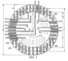
- Figure 5 shows a more detailed view of the support structure shown in Figure 6, wherein the support members comprise rectangular shapes, wherein conductive lines may be routed between the support members and in the central region;
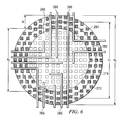
- Figure 6 shows another embodiment of the present invention, wherein the support members comprise square shapes
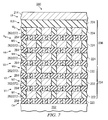
- Figure 7 shows a cross-sectional view of a preferred embodiment of the present invention, wherein the support members are formed in one or more insulating material layers disposed beneath a bond pad;
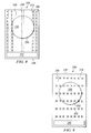
- Figure 8 shows a semiconductor device bond pad region with a plurality of support structures formed in insulating material layers in accordance with an embodiment of the present invention, wherein side supports are used as mechanical support for the bond pad region;
- Figure 9 shows another support structure in accordance with an embodiment of the present invention formed in insulating material layers and comprising a plurality of discrete support structures.
- Figure 1 shows a cross-sectional view of a prior art semiconductor device 100 having a multi-level interconnect structure disposed beneath a bond pad 114.
- the semiconductor device 100 includes a workpiece 102 that may comprise a semiconductor substrate having active components such as transistors and other devices formed thereon.
- a plurality of insulating layers 120, 122, and 124 with vias and conductive lines 112 formed therein is disposed over the workpiece 102.
- a bond pad 114 is formed in a top-most layer LB, disposed in an insulating layer 108.
- the contact array layer CA and via layers V1, V2, V3, Vn, and VLB provide functional electrical connection between the conductive line layers M1, M2, M3, M4, and Mn and the bond pad layer LB, in some locations (not all vias and conductive lines are shown within each layer), for example.
- the insulating layers 122 in region 104 comprise low k insulating layers having a dielectric constant of less than about 3.9.
- the lower level insulating layer 120 in the CA layer may comprise a silicon oxide-based material such as a high density plasma (HDP) oxide or other insulating materials, to provide a strong base for the low k insulating layers 122 in region 104.
- the upper insulating layers 124 in region 106 may comprise silicon dioxide, for example, which is a structurally stronger material.
- the lower conductive layers in region 104 comprise conductive lines 112 and support vias 110 that are smaller and more closely spaced (not shown in the figure) than the conductive lines 112 and vias (not shown) in the upper conductive lines 106, for example.
- the lower conductive material layers in region 104 may include thin cap layers (not shown in Figure 1) disposed over each low k insulating layer 122, to prevent diffusion of copper from conductive lines 112 and support vias 110 into the insulating layer 122, for example.
- the conductive lines 112 and vias in the upper layers 106 may also comprise thicker material layers (also not shown in Figure 1) with relaxed ground rules, for example.
- support structures referred to in the art as copper line and via support (CLVS) structures are typically formed in conductive line and via layers M1, V1, M2, V2, and M3 (e.g., in region 104) of prior art semiconductor devices, e.g., where the insulating material 122 between the conductive lines and vias comprises a low k insulating material.
- Figure 2 shows a top view of a wire bond region 130 of a semiconductor device such as the one shown in Figure 1 having a multi-level interconnect, wherein a prior art CLVS structure comprises conductive support features 140 that comprise an array of alternating metal fingers disposed beneath the bond pad 138, preventing the use of the region beneath the bond pad 138 for wiring.
- Vias 110 are disposed between the conductive support features 140 that are arranged in a mesh or grid-like pattern, alternating by 90 degrees in every other conductive line layer having a low k insulating material (such as layers M1, M2, and M3 in region 104 of Figure 1).
- the circular region 136 represents a wire bond that is adhered or wire bonded to the wire bond pad 138.
- Region 142 comprises a region of stacked metal levels where connection for that particular bond pad 138 is made to underlying conductive line and via levels, for example. Because the conductive support features 140 of the CLVS structure are formed beneath the entire wire bond pad 138, the region beneath the entire wire bond pad 138 cannot be used for functional wiring, resulting in an inefficient use of space on the semiconductor device.
- the support structure 140 is only formed in low k insulating material layers, e.g., in insulating layers 122 in region 104 having a dielectric constant k of less than about 3.9.
- the support structure 140 is not formed in insulating layers 120 and 124 (see the CA layer and region 104, respectively, of Figure 1) having a higher mechanical strength.
- the support structure 140 may include many vias 110 to increase the mechanical stability of the low k insulating material layers 122, for example.
- Embodiments of the present invention provide several novel structures for improved support under bond pads of semiconductor devices.
- support members are formed in an annular shape beneath a wire bond proximate the perimeter of the wire bond.
- support structures are formed in non-low-k insulating material layers, in addition to supports being formed in low k insulating material layers, in various configurations of support structures. These various embodiments will be described further herein.
- Figures 3A through 3C show stress simulation results of a wire bond region 230 at three different bonding forces; low, medium, and high, respectively. Like numerals are used in Figures 3A through 3C as were used in the previous figures.
- the wire bond region 230 includes a wire 232 that is bonded to a wire bond pad (e.g., such as a bond pad 138 in Figure 2, or a bond pad 114 of Figure 1).
- the wire 232 may comprise a thickness of about 20 to 25 ⁇ m or less, and may comprise about 18 ⁇ m, as examples.
- the wire bond 236 may comprise a diameter of about 40 to 50 ⁇ m or less at the bottom surface, and may comprise about 35 ⁇ m, as examples. Alternatively, the wire 232 and wire bond 236 may comprise other dimensions.
- the wire bond 236 substantially comprises the shape of a ball or sphere that is flattened as force is used to bond the wire 232 to the bond pad.
- Figure 3A shows the stress points within a wire bond 236 at a low bonding force, e.g., of about 30 g, as an example, indicating that an area of maximum stress 234 is located at the perimeter of the wire bond 236, e.g., in an annular or ring shape.
- Figure 3B shows the stress points of the wire bond 236 at a medium bonding force, e.g., of about 60 g.
- Figure 3C shows the stress points of the wire bond 236 at a high bonding force, e.g., of 90 g.
- These low, medium, and high bonding forces are used as examples; however, the bonding forces may comprise other values.
- the maximum stress 234 locations of the wire bond 236 proximate the bond pad comprise an annular or ring shape, as shown.
- novel structure supports for bond pads of semiconductor devices are disclosed, wherein the support structures are disposed beneath bond pads in an annular or ring shape in locations where wire bonds will be placed.
- Embodiments of the present invention will be described with respect to preferred embodiments in a specific context, namely semiconductor devices having multiple layers of interconnect. Embodiments of the invention may also be applied, however, to semiconductor devices having a single layer of interconnect, for example.
- Other embodiments of the invention do not comprise ring-shaped support structures, but comprise support members disposed in insulating material layers other than and/or in addition to support members being formed in low k insulating layers, providing increased mechanical stability for the bond pad region, for example.
- FIG. 4 a top view of a wire bond region 230 of a semiconductor device is shown, illustrating the location of the novel support structures of some embodiments of the present invention in relation to a bond pad 238.
- the bond pad 238 is disposed in an upper material layer of a semiconductor device (such as the semiconductor device 100 shown in Figure 1), and the bond pad 238 may comprise aluminum, copper, combinations thereof, or other metals.
- the bond pad 238 may comprise, for example, Ni or Au disposed on top of aluminum.
- the region 242 located to the side of the wire bond 236 comprises an area where the lower metallization layers and conductive line layers are coupled to active areas of the semiconductor device, to make electrical contact to the bond pad 238, for example.
- the support structures are formed in an annular shape where the wire bond 236 will be bonded to the bond pad 238.
- the support structures of some embodiments of the present invention are preferably formed in an annular region 260 to support the maximum stress region, e.g., the perimeter region 234 of a wire bond 236 shown in Figures 3A, 3B, and 3C.
- the annular region 260 dimension may be designed according to the dimensions of the wire bond 236, the strength of the various underlying material layers, and the amount of space needed beneath and/or proximate the wire bond 236 for functional wiring, as examples, although other factors may also be considered.
- the annular region 260 comprises a first diameter d 1 , which may correspond to the maximum width expected for a wire bond 236 after the bonding process.
- a second diameter d 2 is larger than the first diameter d 1 of the annular region 260 by a predetermined amount, to accommodate for variations in the wire bond diameter and other manufacturing process variations.
- the second diameter d 2 is the outer range for the positioning of the novel support structures, to be described further herein.
- the second diameter d 2 comprises the outer diameter of the annular region 260, for example.
- a third diameter d 3 is smaller than the first diameter d 1 of the annular region 260 by the predetermined amount, also to accommodate for variations in the wire bond diameter and other manufacturing processes.
- the third diameter d 3 is the inner range for the positioning of the novel support structures.
- the third diameter d 3 comprises the inner diameter of the annular region 260, for example.
- the predetermined amount may comprise about 1 ⁇ m or greater, for example, although the predetermined amount may comprise other dimensions.
- the predetermined amount may alternatively comprise a percentage of the first diameter d 1 , for example, such as about 10%, although other percentages may also be used.
- the annular region 260 may comprise a ring having a width W that may be calculated based on the first diameter d 1 and the predetermined amount, for example, although other methods may be used to determine the width W.
- the expected dimension of the wire bond 236 or first diameter d 1 is preferably located approximately at a center of the annular region 260, for example.
- the width W of the annular region 260 may comprise about 5 to 10 ⁇ m or less, for example, although the width W may comprise other dimensions.
- the annular region 260 would extend from a diameter d 3 of about 45 ⁇ m to a diameter d 2 of about 55 ⁇ m.
- the width W may comprise other dimensions, depending on the expected ball size of the wire bond 236 after the wire bonding process and/or the predetermined amount (or percentage) used to calculate the width W, as examples.
- the annular region 260 preferably comprises a width W that is large enough to account for potential variation in wire bond 236 ball placement and wire bond 236 size, e.g., from variations in the bonding force used and other processing parameter variations, such as the tolerances of the lithography masks, tools, and wire bonder, as examples.
- support structures are not formed in a central region 268 of the wire bond region 230, e.g., in the middle of the wire bond 236, so that functional wiring may be routed in the central region 268.
- functional wiring may also be routed in a region 269 outside the annular region 260.
- Figure 5 shows a more detailed top view of a wire bond region 230 in an area beneath a wire bond 236 in accordance with an embodiment of the present invention.
- Figure 5 shows a more detailed view of the support structure shown in Figure 4, wherein a plurality of the support members 262 comprises rectangular shapes.
- the support members 262 are formed in at least one conductive line layer of the semiconductor device, disposed beneath a bond pad (e.g., such as bond pad 238 shown in Figure 4).
- Support vias 264 are disposed beneath the rectangular support members 262, e.g., formed in one or more via layers of the semiconductor device.
- the support structure comprises a plurality of the support members 262 disposed substantially in the shape of an annular ring 260, as shown.
- the support members 262 extend from the third or inner diameter d 3 to the second or outer diameter d 2 of the annular region 260, for example, as shown.
- each rectangular support member 262 comprises a width of about 2 to 4 ⁇ m and a length of about 4 to 10 ⁇ m, as examples, although alternatively, the support members 262 may comprise other dimensions.
- the support members 262 may be separated from one another by a distance of about 5 to 10 ⁇ m, for example, although they may also be separated from one another by other distances, particularly if conductive lines 266 are disposed between them, because the conductive lines 266 provide mechanical strength and support.
- the support members 262 may be spaced apart by a distance so that a conductive line 266 may be routed between two adjacent support members 262, e.g., to extend into and/or through the central region 268.
- the conductive lines 266 may comprise a width of about 2 ⁇ m or less, and may alternatively comprise about 0.2 or 0.1 ⁇ m or less, for example.
- the conductive lines 266 may comprise a minimum ground rule or smallest dimension of the semiconductor device, for example.
- the support members 262 are preferably separated from adjacent support members 262 by about 0.5 to 2 ⁇ m, and more preferably, by about 2 ⁇ m or less, in this embodiment, to accommodate for the width of the conductive lines 266, for example.
- One or more of the conductive line layers beneath the bond pad region comprising the support members 262 may be formed using a damascene process.
- a damascene process is one in which an insulating material layer is deposited and patterned, and then filled with a conductive material to form conductive lines (e.g., in a single damascene process), or conductive lines and vias, in a dual damascene process. Excess conductive material is then removed from over the top surface of the insulating material layer using a chemical mechanical polish (CMP) process.
- CMP chemical mechanical polish
- dummy support structures 270 may be formed in the conductive material layers that the support members 262 are formed in, as shown in phantom in Figure 5, for example.
- dummy vias (not shown in the drawing) for each dummy support member may also be formed in the same via levels that the support vias 264 are formed in.
- the dummy support members 270 may comprise a similar shape as the support members 262, or alternatively, the dummy support members 270 may comprise other shapes, for example.
- the dummy support members 270 also improve the lithography processes for the material layers they are formed in, for example.
- the novel support structure comprising a substantially annular shape is preferably formed in at least one first material layer beneath the at least one bond pad.
- the support structure comprises a plurality of support members, wherein the plurality of support members of the support structure comprises a first substantially annular shape beneath the at least one wire bond pad.
- the support structure may be formed in every conductive line layer and material layer over a workpiece, or may be formed in several, or in only one conductive line layer and/or via layer, for example.
- the support structure may be formed in metallization layers, semiconductive material layers, or both, for example.
- Figure 6 shows another embodiment of the present invention, wherein the support members 272 comprise a square shape.
- support vias 264 are preferably disposed beneath the support members 272.
- Dummy support members 274 may optionally be formed in the central region 268, as shown, and conductive lines 266 may be routed between the support members 272, dummy support members 274, and into the central region 268 inside the annular region 260 of support structures.
- the square support members 272 may comprise about 2 to 4 ⁇ m square structures, e.g., in the low k insulating material layers 222, or they may comprise about 4 to 8 ⁇ m square structures, e.g., in upper insulating material layers 224, which are typically thicker, as examples, although alternatively, the support members 272 may comprise other dimensions.
- the support vias 264 may comprise one or more vias.
- an array of a plurality of support vias 264 may be disposed beneath the support members 262 or 272.
- the support vias 264 preferably comprise the size of other vias formed on a semiconductor device.
- the support vias 264 may comprise about 100 nm x 100 nm wide structures, e.g., in the lower low k insulating material layers 222, as shown in Figure 8, or the support vias 264 may comprise about 200 x 200 nm wide structures, e.g., in upper insulating material layers 224, which are typically thicker material layers than the lower insulating material layers 222, as examples, although alternatively, the support vias 264 may comprise other dimensions.
- Figure 7 shows a cross-sectional view of a preferred embodiment of the present invention, wherein the support members 262 or 272 and support vias 264 are formed in one or more conductive material layers disposed beneath a bond pad 214.
- a cross-sectional view of the annular region 260 is shown in Figure 7; in other areas of the semiconductor device 280, e.g., in the central region 268 or areas outside the annular region 260, conductive lines and/or dummy support members (not shown in Figure 7; see Figures 5 and 6) may be formed, for example.
- the support members 262/272 and support vias 264 may comprise metal, such as copper, aluminum, alloys thereof, or other metals or combinations thereof, formed in the BEOL.
- the support members 262/272 and support vias 264 may comprise a semiconductive material, such as polysilicon, e.g., in lower material layers, e.g., formed in the FEOL.
- the support members 262/272 and support vias 264 may be formed by single damascene processes, dual damascene processes, subtractive etch processes, or combinations thereof, for example.
- support members 262/272 and support vias 264 are formed beneath a bond pad 214 in an annular region 260 where the highest amount of stress will be placed on a wire bond (e.g., wire bonds 236 shown in Figures 3A, 3B, and 3C).
- wire bonds 236 shown in Figures 3A, 3B, and 3C.
- the novel support structures described herein provide mechanical and structural support for the bond pad 214 where the support is most needed.
- Other conductive line areas beneath the bond pad 214 may be used for other purposes, such as for forming conductive lines and vias, and/or for forming dummy conductive lines and vias, to improve other processing steps, such as CMP and lithography, as examples.
- Embodiments of the present invention also include methods of manufacturing a semiconductor device 280 comprising the support structures 262/272 and 264 described herein. No additional lithography masks are required to form the novel support structures 262/272 and 264; advantageously, they may be implemented in existing lithography mask levels.
- a workpiece 202 is provided, as shown in Figure 7.
- the workpiece 202 may include a semiconductor substrate comprising silicon or other semiconductor materials that may be covered by an insulating layer, for example.
- the workpiece 202 may include active components or circuits formed in the FEOL, not shown.
- the workpiece 202 may comprise silicon oxide over single-crystal silicon, for example.
- the workpiece 202 may include other conductive layers or other semiconductor elements, e.g. transistors, diodes, etc. Compound semiconductors, GaAs, InP, Si/Ge, or SiC, as examples, may be used in place of silicon.
- the workpiece 202 may also comprise a silicon-on-insulator (SOI) substrate, for example.
- SOI silicon-on-insulator
- An insulating layer 220 comprising a contact array (CA) level may be disposed or formed over the workpiece 202, as shown.
- the insulating layer 220 may comprise a silicon-oxide based insulator such as HDP oxide or other insulating material, and may comprise a plurality of support vias 264 formed therein.
- the insulating layer 220 preferably does not comprise a low k insulating material, for example.
- the support vias 264 may comprise a metal or a semiconductor, for example.
- the support vias 264 may be formed in a damascene or subtractive etch process, for example. Functional vias, not shown, may be formed within the same insulating layer 220 that the support vias 264 are formed in, elsewhere on the semiconductor device 100.
- a plurality of insulating layers 222 are sequentially formed over the insulating layer 220 and support vias 264, and alternating layers of support members 262 or 272 and support vias 264 are formed in the insulating layers 222.
- the insulating layers 222 may comprise a low k dielectric material, or each layer may comprise a combination or multi-layers of silicon dioxide, silicon nitride, or other materials and a low k dielectric material, in region 204, as examples.
- the insulating layers 222 may comprise about 300 nm or less of SiO 2 , SiN, carbon-doped oxides, organic dielectric materials, or low-k insulating materials, or combinations thereof.
- the insulating layers 222 may comprise low k insulating materials such as Black Diamond TM from Applied Materials, SiCOH, Coral TM from Novellus Systems Inc., Aurora TM from ASM International, or other low k materials, as examples.
- the support members 262/272 and support vias 264 in two adjacent insulating layers 222 may be formed in a dual damascene process, for example, although single damascene processes and subtractive etch processes may also be used.
- Functional vias and functional conductive lines may be formed within the same insulating layers 222 that the support vias 264 and support members 262/272 are formed in, elsewhere on the semiconductor device 100.
- the insulating layers 222 in region 204 are also referred to as M1, V1, M2, V2, and M3 layers, as shown.
- the insulating layers 222 may include cap layers (not shown) disposed over the low k insulating material, to prevent the conductive material such as copper from diffusing into the low k insulating material, for example.
- a plurality of insulating layers 224 in region 206 is formed over the insulating layers 222 in region 204.
- Support members 262/272 and support vias 264 are preferably formed in alternating insulating layers 222, as shown, in V3, M4, V4, M5, Vn, and Mn layers disposed sequentially over the M3 layer of region 204, as shown.
- the plurality of insulating layers 224 in region 206 preferably does not comprise low k insulating materials, in some embodiments.
- the insulating layers 224 may comprise SiO 2 , fluorinated spin on glass (FSG), fluorinated tetra ethyl oxysilane (TEOS), n-BLOk TM from Applied Materials, or hybrids or multiple layers thereof, as examples, although other materials may also be used.
- the V3, M4, V4, M5, Vn, Mn, and VLB layers are typically thicker and may include or comprise a hard mask for increased mechanical stability, than the M1, V1, M2, V2, and M3 layers, for example.
- the V3, M4, V4, M5, Vn, Mn, and VLB layers may comprise a thickness of about 500 nm or more, for example.
- Support vias 264 are typically not formed within insulating layer 224 of layer VLB, to avoid interfering with the electrical wiring of the semiconductor device 280, e.g., with the wiring of the bond pad 214 to an underlying conductive line.
- Functional conductive lines and vias may be formed within the same insulating layers 224 that the support vias 264 and support members 262/272 are formed in, elsewhere on the semiconductor device 280.
- the insulating material layers 220, 222, and 224 may include optional capping layers and/or liners comprised of various materials, such as nitrides or oxides, as examples, not shown.
- the support members 262/272 and support vias 264 preferably comprise the same material used for the conductive line or conductive via layer they are formed in.
- the support members 262/272 and support vias 264 preferably comprise copper or a copper alloy in one embodiment, although alternatively, the support members 262/272 and support vias 264 may comprise other conductive materials, such as aluminum or aluminum alloys, as examples.
- a barrier layer and/or liner may be deposited over the insulating layers 220, 222, and 224 before depositing conductive material to form the support members 262/272 and support vias 264, for example, not shown.
- the support members 262 or 272 and support vias 264 may be formed in one or more conductive layers of a semiconductor device 100.
- the support members 262 or 272 and support vias 264 are formed in every conductive line layer disposed beneath a bond pad, in an annular shape disposed beneath the region where a wire bond will be formed, proximate the perimeter of the wire bond.
- the support members 262 and 272 may also be formed in a contact level, (e.g., CA layer) for example.
- Processing of the semiconductor device 280 is then continued. For example, integrated circuits on a workpiece 202 are singulated to form individual die, and then wire bonds are attached to the bond pads 214 using a wire bonding process, to package the individual die or couple the die to other individual die in a multi-chip module, for example.
- Embodiments of the present invention also include methods of designing semiconductor devices 280.
- the design methods include designing a semiconductor device 280 active region, e.g., within a workpiece 202 as shown in Figure 7, and determining a bond pad 214 layout for the semiconductor device 280.
- a first diameter d 1 for a wire bond (e.g., such as wire bond 236 shown in Figures 3A, 3B, and 3C) that will be bonded to each bond pad 214 is determined.
- a layout for at least one conductive line layer (e.g., one or more of layers M1, M2, M3, M4, M5, Mn) is determined for the semiconductor device 280 to be located between the active region 202 and the bond pads 214, wherein the at least one conductive line layer layout includes a plurality of support members 262 or 272 arranged in a substantially annular shape proximate a perimeter of a wire bond region of each bond pad 214.
- the plurality of support members preferably comprises a diameter, wherein the diameter of the plurality of support members is substantially equal to the first diameter d 1 of the wire bond.
- a layout for at least one via layer (e.g., one or more of layers CA, V1, V2, V3, V4, or Vn) is designed to be adjacent the layout for the at least one conductive line layer, wherein the at least one via layer layout includes a plurality of support vias 264 proximate each of the plurality of support members 262/272.
- the at least one bond pad region of a semiconductor device comprises at least one bond pad and further comprises a wire bond coupled to the at least one bond pad.
- the wire bond comprises a perimeter
- the first support members and the plurality of second support members comprise a plurality of support members arranged in a substantially annular shape disposed beneath and proximate the perimeter of the wire bond.
- the support structures and support vias 264 may be formed in alternating rows and columns, e.g., forming alternating fingers of metal, as shown in Figure 2.
- the support structures are formed in the entire bond pad region, rather than being formed in an annular shape, as described for the embodiments shown in Figures 4, 5 and 6.
- support structures may be formed in one metal layer M1 in rows running horizontally from left to right on the page, and support structures may be formed in an adjacent metal layer M2 in columns running vertically in and out of the page, with support vias 264 being disposed at intersections of the rows and columns, creating a multi-layer mesh support structure.
- the support structures and vias may comprise the shape of the prior art support structures and vias of the prior art Figure 2
- the support structures are formed not only in the low k insulating layers 222 as in the prior art, but the support structures and vias are also preferably formed in the insulating layer 220 disposed between the workpiece 202 and the low k insulating layers 222, which anchors the low k insulating layers 222 to the workpiece 202, preventing CTE mismatch delaminations.
- the support structures may also be formed in the insulating layers 224 in region 206 disposed between the low k insulating layers 222 in region 204 and the bond pad 214, providing increased structural support.
- the interwoven mesh support structures may be formed both in insulating layer 220 and in insulating layers 224 in region 206, e.g., with support vias 264 being disposed between each insulating layer 220, 222, and 224, so that the support structures are formed in every insulating layer 220, 222, and 224 disposed between the workpiece 202 and the bond pad 214, other than the insulating layer for layer VLB immediately beneath the bond pad 214, for example.
- Embodiments of the present invention also include support structures formed in non-low k insulating layers, wherein the support structures comprise other configurations.
- support structures formed only at the sides, or at both the sides and a central strip of a bond pad region, as shown Figure 8 may be formed in low k insulating layers 222 and also in insulating layer 220, insulating layers 224, or both insulating layer 220 and insulating layers 224.
- discrete support structures as shown in Figure 9 may be formed in low k insulating layers 222 and also in insulating layer 220, insulating layers 224, or both insulating layer 220 and insulating layers 224.
- a semiconductor device bond pad region 230 includes a support structure for the bond pad region 230.
- conductive side support features 244 and vias 210 are formed in the metallization layers having both low k insulating material (such as layers M1, M2, and M3 in region 204 of Figure 7) and also metallization layers having non-low k insulating material (such as layers M4, M5, and M n in region 206, or in CA layer) beneath the wire bond pad 238 at the sides of a wire bond 236, which allows for functional wiring to be routed beneath and proximate a portion 248 of the wire bond 236 and wire bond region 230.
- low k insulating material such as layers M1, M2, and M3 in region 204 of Figure 7
- non-low k insulating material such as layers M4, M5, and M n in region 206, or in CA layer
- conductive side support features 244 and vias 210 By forming the conductive side support features 244 and vias 210 in the metallization layers having non-low k insulating material, improved structural support is provided for the wire bond region 230, for example.
- functional wiring is possible in a direction parallel to the rows of the side supports 244 formed at the edges beneath the wire bond region 230, in this embodiment.
- FIG. 8 An alternative embodiment to the support structure shown in Figure 8 that provides additional structural support is to include a central support member 246, shown in phantom in Figure 8, that is placed parallel to and between the side support features 844, beneath the center of the wire bond 236. While the use of functional wiring is further limited by the use of the additional central support 246 beneath and proximate a portion 248 of the wire bond 236, this embodiment provides an increased amount of support for the wire bond region 230.
- Figure 9 shows another embodiment of the present invention, wherein a support structure for a wire bond region comprises a plurality of discrete support structures 252.
- the discrete support structures 252 comprise conductive regions and vias 210 formed in the metallization layers having low k insulating materials (such as layers M1, M2, and M3 in region 204 of Figure 7) and also metallization layers having non-low k insulating material (such as layers M4, M5, and M n in region 206, or in CA layer), beneath the wire bond pad 238 at predetermined locations, e.g., disposed in an array beneath the wire bond 236.
- the discrete support structures 252 are preferably placed about 5 to 10 ⁇ m apart, for example, and are preferably evenly distributed beneath the bond pad 238, for example. This support structure also allows the placement of functional wiring in portions 248 of the area beneath and proximate the wire bond 136.
- the support structures shown in Figures 8 and 9 do not provide support in all perimeter areas of the wire bond 236, wherein the support is most needed. For this reason, the embodiments shown in Figures 8 and 9 comprise less-preferred embodiments of the present invention.
- the two rows of supports 244 on a first side of the wire bond 236 and a second opposing side of the wire bond 236 do not provide support in the central region or at the sides of the wire bond 236 rotated 90 degrees from the rows of supports 244, e.g., at 250.
- the support structures are preferably formed not only in the low k insulating layers 222, but also in either the insulating layer 220, the insulating layers 224, or both, the support structures in the low k insulating layers 222 are anchored to the workpiece 202 and/or to the overlying support structures, providing a much more mechanically strong structure throughout the various material layers. Mechanical stress may be dissipated through vias and support structures into the silicon of the workpiece 202, resulting in reduced stress in the low k insulating layers 222. The risk of tear outs during wire bond tests is therefore reduced.
- the support members and the support vias beneath bond pads are formed in an annular shape beneath bond pads of a semiconductor device, proximate a perimeter of a wire bond that will be formed later in a wire bonding process.
- the support structures are formed in conductive line and via layers of a semiconductor device. Areas that are not used for the support members and support vias (e.g.
- region 268 inside the annular region 260 and/or region 269 outside the annular region 260, as shown in Figure 6) may be used for functional wiring and/or for dummy structures to improve CMP and lithography processes, allowing for semiconductor devices to be decreased in size, because the region 268 within the annular support members and the region 269 (see Figure 4) outside the annular support members can be used for wiring.
- the reduction in size of semiconductor devices also results in a decreased cost.
- the largest amount of area possible is left unused under bond pads and/or active devices, resulting in the largest amount of area being made available for routing functional conductive lines.
- the risk of delamination of low k insulating material layers, and the risk of tear outs during wire bond tests, are both reduced.
- the annular shaped support members may be formed in low k insulating material layers only, or also in other insulating material layers of a semiconductor device, such as upper metallization layers in region 206 not having a low k insulating material, and also in the contact array CA level, as shown in Figure 7.
Landscapes
- Internal Circuitry In Semiconductor Integrated Circuit Devices (AREA)
Abstract
Description
- The present invention relates generally to the fabrication of semiconductor devices, and more particularly to the formation of support structures for wire bonding areas of semiconductor devices.
- Semiconductor devices are used in a variety of electronic applications, such as computers, cellular phones, personal computing devices, and many other applications. Home, industrial, and automotive devices that in the past comprised only mechanical components now have electronic parts that require semiconductor devices, for example.
- Semiconductor devices typically include several layers of insulating, conductive and semiconductive materials that are patterned to form integrated circuits. There may be a plurality of transistors, memory devices, switches, conductive lines, diodes, capacitors, logic circuits, and other electronic components formed on a single die or chip. Semiconductor technology has seen a trend towards miniaturization, to meet the demands of product size reduction, improved device performance, and reduced power requirements in the end applications that semiconductors are used in, for example.
- The manufacturing process for semiconductor devices is typically referred to in two phases: the front-end-of-line (FEOL) and the back-end-of-line (BEOL). The FEOL is typically defined as the processing steps that begin with a starting semiconductor wafer or workpiece up to the formation of the first metallization layer, and the BEOL is defined as the processing steps from that point forward, for example.
- In the past, integrated circuits contained a relatively small number of devices per chip or die, and the devices could be easily interconnected. However, in more recent integrated circuit designs, there may be hundreds or thousands of devices on a single chip, resulting in the need for multilevel interconnect systems, wherein the area for interconnect lines is shared among two or more material levels.
- As the minimum line width on integrated circuits becomes smaller, the active device density increases, and the time required for transistors to charge capacitive loads becomes limiting on the performance of the integrated circuit. Also, as the chip size increases, the interconnect path lengths also increase. Thus, many large ultra-large scale integration (ULSI) circuits are limited by interconnect propagation delay time. The propagation delay of integrated circuits becomes limited by the RC delay of the interconnection lines when the minimum feature size decreases below about 1 µm, for example, which limits the circuit speeds. The RC delay refers to the resistance (R) of the conductive lines used for the interconnect lines and the capacitance (C) between the conductive lines.
- One challenge in the semiconductor industry is to reduce and minimize the RC delay of integrated circuits, in order to improve device performance and increase device speed. The resistive or R component of RC delay is being addressed by a move from the use of aluminum to copper, which has a lower resistance than aluminum, as the material for conductive lines. The C or capacitive component of RC delay is being addressed by the use of insulating materials between the conductive lines that comprise a lower dielectric constant (k) than materials such as SiO2 that were used in the past for inter-metal dielectric (IMD). However, most low k insulating materials are structurally weak.
- Another challenge in fabricating semiconductor devices is that electrical contact must be made from the very small chip or integrated circuit to leads of a package, or to other chips, in a multi-chip module, for example. The electrical contact to an integrated circuit is made using wire bonds that are wire bonded to bond pads on the chips. The wire bonding process involves placing a wire, typically comprising gold or other metal, against a bond pad on the integrated circuit, and applying pressure to the wire while vibrating the wire, causing the wire to become bonded to the bond pad. Destructive wire bond strength tests (e.g., the test chips are discarded after the tests) are typically performed on a small number of semiconductor devices in a lot after the wire bonding process, in which an upward force is applied to a wire to determine how much force it takes to lift the wire from the bond pad.
- If the material layers beneath the bond pad are weak, the semiconductor device may be damaged during the wire bonding process. Furthermore, when tests on the wire bonds are performed, damage and lift-off of the bond pads can occur. For example, portions of the material layers beneath and adjacent the bond pad may be pulled away or lifted during the wire bond strength tests. The introduction of low k materials as insulating materials in semiconductor device manufacturing has made pad stacks for wire bonding more critical because of the weaker material properties of the low k materials.
- Therefore, some recent semiconductor designs have support structures formed in the metallization layers beneath the bond pads in the low k insulating material layers. However, some of these prior art support structures take up valuable real estate on chips. For example, the presence of support structures in the bond pad region prohibits or limits the use of the area under the bond pads from being used as functional conductive lines, e.g., for the electrical wiring of the semiconductor device, in the low k insulating material layers.
- Furthermore, prior art support structures are formed only in conductive line and via layers having a low k material, e.g., comprising a dielectric constant of less than the dielectric constant of SiO2, or having a k value of less than about 3.9. Forming support structures in only the low k material layers causes stress fractures, delamination of the low k material due to sheer force stress, and an increased risk of tear-outs during wire bond tests, for example.
- Thus, what are needed in the art are improved support structures for providing mechanical support for wire bond areas of semiconductor devices, particularly in semiconductor devices having low k insulating materials as dielectric layers.
- These and other problems are generally solved or circumvented, and technical advantages are generally achieved, by preferred embodiments of the present invention, which provide novel support structures and methods of forming thereof, disposed beneath bond pads of semiconductor devices. In some embodiments, the support structures comprise support members that are primarily formed in regions where the support is needed the most, e.g., in the regions proximate the perimeter of a wire bond that is bonded to the bond pad. Functional conductive lines may then be formed in the central region beneath the bond pad and between the support members. In other embodiments, support structures are formed not only in the low k insulating material layers, but also in the other, non-low k insulating material layers, anchoring the support structures to the workpiece or substrate, or to the upper material layers of the semiconductor device.
- In accordance with a preferred embodiment of the present invention, a semiconductor device includes a workpiece, at least one first material layer disposed over the workpiece, and a second material layer disposed over the at least one first material layer. The second material layer includes at least one bond pad. A support structure is disposed in the at least one first material layer beneath the at least one bond pad. The support structure comprises a plurality of support members, wherein the plurality of support members of the support structure comprises a first substantially annular shape beneath the at least one wire bond pad.
- In accordance with another preferred embodiment of the present invention, a semiconductor device includes a workpiece, at least one first material layer disposed over the workpiece, and a second material layer disposed over the at least one first material layer. The second material layer includes at least one bond pad, and a wire bond is coupled to the at least one bond pad. The wire bond comprises maximum stress regions adjacent the at least one bond pad. A support structure is disposed in the at least one first material layer proximate the maximum stress regions of the wire bond.
- In accordance with another preferred embodiment of the present invention, a method of manufacturing a semiconductor device includes providing a workpiece, forming at least one first material layer over the workpiece, and forming a second material layer over the at least one first material layer, the second material layer including at least one bond pad. Forming the at least one first material layer includes forming a support structure in the at least one first material layer beneath the at least one bond pad, the support structure comprising a plurality of support members, wherein the plurality of support members comprises a first substantially annular shape beneath the at least one wire bond pad.
- In accordance with yet another preferred embodiment of the present invention, a method of designing a semiconductor device includes designing a semiconductor device active region, determining a layout for a plurality of bond pads to be disposed over the semiconductor device active region, determining a first diameter for a perimeter of a wire bond that will be bonded to each of the plurality of bond pads, and designing a layout for at least one conductive line layer for the semiconductor device to be disposed between the active region and the plurality of bond pads. The layout for the at least one conductive line layer includes a plurality of support members arranged in a substantially annular shape proximate a perimeter of the wire bond to be bonded to each bond pad. The annular shape of the plurality of support members comprises a second diameter, wherein the second diameter is substantially equal to the first diameter.
- In accordance with another preferred embodiment of the present invention, a semiconductor device includes a workpiece and a first low k insulating material layer disposed over the workpiece. The first low k insulating material layer comprises a first dielectric constant, and a plurality of first support vias are formed in the first low k insulating material layer. A second low k insulating material layer comprising the first dielectric constant is disposed over the first low k insulating material layer. A plurality of first support members is formed in the second low k insulating material layer, wherein the plurality of first support vias makes contact with the plurality of first support members. At least one bond pad region is disposed over the second low k insulating material layer, wherein the plurality of first support vias and the plurality of first support members provide mechanical support for the at least one bond pad region. At least one first insulating material layer comprising a second dielectric constant is disposed either between the workpiece and the first low k insulating material layer or between the second low k insulating material layer and the at least one bond pad region, or both. The second dielectric constant is greater than the first dielectric constant, and a plurality of second support members are formed in the at least one first insulating material layer.
- Advantages of preferred embodiments of the present invention include providing structural supports for wire bond regions while allowing the formation of functional conductive lines under bond pads of a semiconductor device, saving space. Smaller semiconductor devices can be manufactured, e.g., current designs may be scaled down in size, in accordance with embodiments of the present invention. Semiconductor devices with more stable mechanical structures beneath bond pads are provided.
- The foregoing has outlined rather broadly the features and technical advantages of embodiments of the present invention in order that the detailed description of the invention that follows may be better understood. Additional features and advantages of embodiments of the invention will be described hereinafter, which form the subject of the claims of the invention. It should be appreciated by those skilled in the art that the conception and specific embodiments disclosed may be readily utilized as a basis for modifying or designing other structures or processes for carrying out the same purposes of the present invention. It should also be realized by those skilled in the art that such equivalent constructions do not depart from the spirit and scope of the invention as set forth in the appended claims.
- For a more complete understanding of the present invention, and the advantages thereof, reference is now made to the following descriptions taken in conjunction with the accompanying drawings, in which:
- Figure 1 shows a cross-sectional view of a prior art semiconductor device having a multi-level interconnect structure disposed beneath a bond pad;
- Figure 2 shows a top view of a prior art copper line and via support (CLVS) structure formed in low k insulating material layers, wherein the CLVS structure has alternating metal fingers beneath the bond pad, preventing the use of the region beneath the bond pad for wiring;
- Figures 3A through 3C show stress simulation results of a wire bond at three different bonding forces, revealing that the area of maximum stress of the wire bond resides in regions proximate the perimeter of the wire bond;
- Figure 4 shows a top view of a bond pad in accordance with an embodiment of the present invention, wherein a plurality of support members are disposed in an annular shape beneath and proximate the perimeter of a wire bond;
- Figure 5 shows a more detailed view of the support structure shown in Figure 6, wherein the support members comprise rectangular shapes, wherein conductive lines may be routed between the support members and in the central region;
- Figure 6 shows another embodiment of the present invention, wherein the support members comprise square shapes; and
- Figure 7 shows a cross-sectional view of a preferred embodiment of the present invention, wherein the support members are formed in one or more insulating material layers disposed beneath a bond pad;
- Figure 8 shows a semiconductor device bond pad region with a plurality of support structures formed in insulating material layers in accordance with an embodiment of the present invention, wherein side supports are used as mechanical support for the bond pad region;
- Figure 9 shows another support structure in accordance with an embodiment of the present invention formed in insulating material layers and comprising a plurality of discrete support structures.
- Corresponding numerals and symbols in the different figures generally refer to corresponding parts unless otherwise indicated. The figures are drawn to clearly illustrate the relevant aspects of the preferred embodiments and are not necessarily drawn to scale.
- The making and using of the presently preferred embodiments are discussed in detail below. It should be appreciated, however, that the present invention provides many applicable inventive concepts that can be embodied in a wide variety of specific contexts. The specific embodiments discussed are merely illustrative of specific ways to make and use the invention, and do not limit the scope of the invention.
- Figure 1 shows a cross-sectional view of a prior
art semiconductor device 100 having a multi-level interconnect structure disposed beneath abond pad 114. Thesemiconductor device 100 includes aworkpiece 102 that may comprise a semiconductor substrate having active components such as transistors and other devices formed thereon. A plurality of insulatinglayers conductive lines 112 formed therein is disposed over theworkpiece 102. Abond pad 114 is formed in a top-most layer LB, disposed in an insulatinglayer 108. The contact array layer CA and via layers V1, V2, V3, Vn, and VLB provide functional electrical connection between the conductive line layers M1, M2, M3, M4, and Mn and the bond pad layer LB, in some locations (not all vias and conductive lines are shown within each layer), for example. - The insulating
layers 122 inregion 104 comprise low k insulating layers having a dielectric constant of less than about 3.9. The lowerlevel insulating layer 120 in the CA layer may comprise a silicon oxide-based material such as a high density plasma (HDP) oxide or other insulating materials, to provide a strong base for the lowk insulating layers 122 inregion 104. The upper insulatinglayers 124 inregion 106 may comprise silicon dioxide, for example, which is a structurally stronger material. The lower conductive layers inregion 104 compriseconductive lines 112 and support vias 110 that are smaller and more closely spaced (not shown in the figure) than theconductive lines 112 and vias (not shown) in the upperconductive lines 106, for example. The lower conductive material layers inregion 104 may include thin cap layers (not shown in Figure 1) disposed over each lowk insulating layer 122, to prevent diffusion of copper fromconductive lines 112 and support vias 110 into the insulatinglayer 122, for example. Theconductive lines 112 and vias in theupper layers 106 may also comprise thicker material layers (also not shown in Figure 1) with relaxed ground rules, for example. - Because the insulating
layers 122 in conductive material layers, M1, V1, M2, V2, M3 inregion 104 that comprise low k materials require more structural support beneath abond pad 114, support structures referred to in the art as copper line and via support (CLVS) structures are typically formed in conductive line and via layers M1, V1, M2, V2, and M3 (e.g., in region 104) of prior art semiconductor devices, e.g., where the insulatingmaterial 122 between the conductive lines and vias comprises a low k insulating material. - A prior art CLVS structure for bond pads will next be described. Like numerals are used for the elements in Figure 2 as were used in the previous figure.
- Figure 2 shows a top view of a
wire bond region 130 of a semiconductor device such as the one shown in Figure 1 having a multi-level interconnect, wherein a prior art CLVS structure comprises conductive support features 140 that comprise an array of alternating metal fingers disposed beneath the bond pad 138, preventing the use of the region beneath the bond pad 138 for wiring.Vias 110 are disposed between the conductive support features 140 that are arranged in a mesh or grid-like pattern, alternating by 90 degrees in every other conductive line layer having a low k insulating material (such as layers M1, M2, and M3 inregion 104 of Figure 1). Thecircular region 136 represents a wire bond that is adhered or wire bonded to the wire bond pad 138.Region 142 comprises a region of stacked metal levels where connection for that particular bond pad 138 is made to underlying conductive line and via levels, for example. Because the conductive support features 140 of the CLVS structure are formed beneath the entire wire bond pad 138, the region beneath the entire wire bond pad 138 cannot be used for functional wiring, resulting in an inefficient use of space on the semiconductor device. - Another problem with the prior
art CLVS structure 140 shown in Figure 2 is that thesupport structure 140 is only formed in low k insulating material layers, e.g., in insulatinglayers 122 inregion 104 having a dielectric constant k of less than about 3.9. Thesupport structure 140 is not formed in insulatinglayers 120 and 124 (see the CA layer andregion 104, respectively, of Figure 1) having a higher mechanical strength. Thesupport structure 140 may includemany vias 110 to increase the mechanical stability of the low k insulating material layers 122, for example. However, because only the lowk insulating layers 122 are stabilized withsupport structure 140, and because there is no connection to the insulatinglayers workpiece 102, differences in the coefficients of thermal expansion (CTE) of the insulating layers 120,122, and 124 can lead to shear forces between the different material layers, which can result in delamination. Tear-outs have been observed after wire bond pull tests, which shows a weakness in these semiconductor device structures. - Embodiments of the present invention provide several novel structures for improved support under bond pads of semiconductor devices. In some embodiments, support members are formed in an annular shape beneath a wire bond proximate the perimeter of the wire bond. In other embodiments, support structures are formed in non-low-k insulating material layers, in addition to supports being formed in low k insulating material layers, in various configurations of support structures. These various embodiments will be described further herein.
- In embodiments of the present invention where a substantially annular support structure is used, technical advantages are achieved by placing support structures beneath wire bond pad regions of a semiconductor device in the locations where the support is most needed. Figures 3A through 3C show stress simulation results of a
wire bond region 230 at three different bonding forces; low, medium, and high, respectively. Like numerals are used in Figures 3A through 3C as were used in the previous figures. - The
wire bond region 230 includes awire 232 that is bonded to a wire bond pad (e.g., such as a bond pad 138 in Figure 2, or abond pad 114 of Figure 1). Thewire 232 may comprise a thickness of about 20 to 25 µm or less, and may comprise about 18 µm, as examples. Thewire bond 236 may comprise a diameter of about 40 to 50 µm or less at the bottom surface, and may comprise about 35 µm, as examples. Alternatively, thewire 232 andwire bond 236 may comprise other dimensions. - The
wire bond 236 substantially comprises the shape of a ball or sphere that is flattened as force is used to bond thewire 232 to the bond pad. Figure 3A shows the stress points within awire bond 236 at a low bonding force, e.g., of about 30 g, as an example, indicating that an area ofmaximum stress 234 is located at the perimeter of thewire bond 236, e.g., in an annular or ring shape. Figure 3B shows the stress points of thewire bond 236 at a medium bonding force, e.g., of about 60 g. Figure 3C shows the stress points of thewire bond 236 at a high bonding force, e.g., of 90 g. These low, medium, and high bonding forces are used as examples; however, the bonding forces may comprise other values. - Note that as the wire bonding force is increased, the height of the
wire bond 236 is decreased, and the diameter of thewire bond 236 is increased. The stress simulation results show that stress is not evenly distributed within awire bond 236; rather, the highest amount of stress was found to be at the edge of thewire bond 236, e.g., at the perimeter of the substantially circular structure of thewire bond 236. Therefore, when awire 232 is bonded to a bond pad of a semiconductor device, themaximum stress 234 locations of thewire bond 236 proximate the bond pad comprise an annular or ring shape, as shown. - In some embodiments of the present invention, novel structure supports for bond pads of semiconductor devices are disclosed, wherein the support structures are disposed beneath bond pads in an annular or ring shape in locations where wire bonds will be placed. Embodiments of the present invention will be described with respect to preferred embodiments in a specific context, namely semiconductor devices having multiple layers of interconnect. Embodiments of the invention may also be applied, however, to semiconductor devices having a single layer of interconnect, for example. Other embodiments of the invention do not comprise ring-shaped support structures, but comprise support members disposed in insulating material layers other than and/or in addition to support members being formed in low k insulating layers, providing increased mechanical stability for the bond pad region, for example.
- With reference next to Figure 4, a top view of a
wire bond region 230 of a semiconductor device is shown, illustrating the location of the novel support structures of some embodiments of the present invention in relation to abond pad 238. Like numerals are used in Figure 4 as were used in the previous figures. Thebond pad 238 is disposed in an upper material layer of a semiconductor device (such as thesemiconductor device 100 shown in Figure 1), and thebond pad 238 may comprise aluminum, copper, combinations thereof, or other metals. Thebond pad 238 may comprise, for example, Ni or Au disposed on top of aluminum. Theregion 242 located to the side of thewire bond 236 comprises an area where the lower metallization layers and conductive line layers are coupled to active areas of the semiconductor device, to make electrical contact to thebond pad 238, for example. - The support structures are formed in an annular shape where the
wire bond 236 will be bonded to thebond pad 238. For example, the support structures of some embodiments of the present invention are preferably formed in anannular region 260 to support the maximum stress region, e.g., theperimeter region 234 of awire bond 236 shown in Figures 3A, 3B, and 3C. Theannular region 260 dimension may be designed according to the dimensions of thewire bond 236, the strength of the various underlying material layers, and the amount of space needed beneath and/or proximate thewire bond 236 for functional wiring, as examples, although other factors may also be considered. - For purposes of discussion, several diameters with respect to a
wire bond 236 and anannular region 260 for the formation of the novel support structures for bond regions of semiconductor devices in accordance with embodiments of the present invention will next be described. Theannular region 260 comprises a first diameter d1, which may correspond to the maximum width expected for awire bond 236 after the bonding process. - A second diameter d2 is larger than the first diameter d1 of the
annular region 260 by a predetermined amount, to accommodate for variations in the wire bond diameter and other manufacturing process variations. The second diameter d2 is the outer range for the positioning of the novel support structures, to be described further herein. The second diameter d2 comprises the outer diameter of theannular region 260, for example. - A third diameter d3 is smaller than the first diameter d1 of the
annular region 260 by the predetermined amount, also to accommodate for variations in the wire bond diameter and other manufacturing processes. The third diameter d3 is the inner range for the positioning of the novel support structures. The third diameter d3 comprises the inner diameter of theannular region 260, for example. - The predetermined amount may comprise about 1 µm or greater, for example, although the predetermined amount may comprise other dimensions. The predetermined amount may alternatively comprise a percentage of the first diameter d1, for example, such as about 10%, although other percentages may also be used.
- The
annular region 260 may comprise a ring having a width W that may be calculated based on the first diameter d1 and the predetermined amount, for example, although other methods may be used to determine the width W. The expected dimension of thewire bond 236 or first diameter d1 is preferably located approximately at a center of theannular region 260, for example. The width W of theannular region 260 may comprise about 5 to 10 µm or less, for example, although the width W may comprise other dimensions. - As an example, if a
wire bond 236 is expected to have a diameter of about 50 µm, the predetermined amount used to calculate the width W may comprise about +/- about 10% of the first diameter d1, then the width W may be calculated using Eq. 1:
Thus, in this example, theannular region 260 would extend from a diameter d3 of about 45 µm to a diameter d2 of about 55 µm. - As another example, the predetermined amount may comprise a fixed dimension, rather than a percentage. If the predetermined amount comprises 2 µm, and if a
wire bond 236 is expected to have a diameter of about 40 µm, the width W may be calculated as shown in Equation 2:
and theannular region 260 would extend from a third diameter d3 of about 38 µm to a second diameter d2 of about 42 µm. Alternatively, the width W may comprise other dimensions, depending on the expected ball size of thewire bond 236 after the wire bonding process and/or the predetermined amount (or percentage) used to calculate the width W, as examples. - The
annular region 260 preferably comprises a width W that is large enough to account for potential variation inwire bond 236 ball placement andwire bond 236 size, e.g., from variations in the bonding force used and other processing parameter variations, such as the tolerances of the lithography masks, tools, and wire bonder, as examples. Preferably, support structures are not formed in acentral region 268 of thewire bond region 230, e.g., in the middle of thewire bond 236, so that functional wiring may be routed in thecentral region 268. Advantageously, functional wiring may also be routed in aregion 269 outside theannular region 260. - Figure 5 shows a more detailed top view of a
wire bond region 230 in an area beneath awire bond 236 in accordance with an embodiment of the present invention. Figure 5 shows a more detailed view of the support structure shown in Figure 4, wherein a plurality of thesupport members 262 comprises rectangular shapes. Thesupport members 262 are formed in at least one conductive line layer of the semiconductor device, disposed beneath a bond pad (e.g., such asbond pad 238 shown in Figure 4).Support vias 264 are disposed beneath therectangular support members 262, e.g., formed in one or more via layers of the semiconductor device. The support structure comprises a plurality of thesupport members 262 disposed substantially in the shape of anannular ring 260, as shown. Preferably, thesupport members 262 extend from the third or inner diameter d3 to the second or outer diameter d2 of theannular region 260, for example, as shown. - In this embodiment, each
rectangular support member 262 comprises a width of about 2 to 4 µm and a length of about 4 to 10 µm, as examples, although alternatively, thesupport members 262 may comprise other dimensions. Thesupport members 262 may be separated from one another by a distance of about 5 to 10 µm, for example, although they may also be separated from one another by other distances, particularly ifconductive lines 266 are disposed between them, because theconductive lines 266 provide mechanical strength and support. For example, in some areas of theannular region 260, thesupport members 262 may be spaced apart by a distance so that aconductive line 266 may be routed between twoadjacent support members 262, e.g., to extend into and/or through thecentral region 268. Theconductive lines 266 may comprise a width of about 2 µm or less, and may alternatively comprise about 0.2 or 0.1 µm or less, for example. Theconductive lines 266 may comprise a minimum ground rule or smallest dimension of the semiconductor device, for example. Thesupport members 262 are preferably separated fromadjacent support members 262 by about 0.5 to 2 µm, and more preferably, by about 2 µm or less, in this embodiment, to accommodate for the width of theconductive lines 266, for example. - One or more of the conductive line layers beneath the bond pad region comprising the
support members 262 may be formed using a damascene process. A damascene process is one in which an insulating material layer is deposited and patterned, and then filled with a conductive material to form conductive lines (e.g., in a single damascene process), or conductive lines and vias, in a dual damascene process. Excess conductive material is then removed from over the top surface of the insulating material layer using a chemical mechanical polish (CMP) process. - One concern during CMP processes is the even removal of conductive material, and the avoidance of dishing or excess removal of the insulating material layers, in order to maintain planarity in the various material layers. To improve the CMP process and results, in accordance with some embodiments of the present invention,
dummy support structures 270 may be formed in the conductive material layers that thesupport members 262 are formed in, as shown in phantom in Figure 5, for example. Likewise, dummy vias (not shown in the drawing) for each dummy support member may also be formed in the same via levels that the support vias 264 are formed in. Thedummy support members 270 may comprise a similar shape as thesupport members 262, or alternatively, thedummy support members 270 may comprise other shapes, for example. Thedummy support members 270 also improve the lithography processes for the material layers they are formed in, for example. - The novel support structure comprising a substantially annular shape is preferably formed in at least one first material layer beneath the at least one bond pad. The support structure comprises a plurality of support members, wherein the plurality of support members of the support structure comprises a first substantially annular shape beneath the at least one wire bond pad. The support structure may be formed in every conductive line layer and material layer over a workpiece, or may be formed in several, or in only one conductive line layer and/or via layer, for example. The support structure may be formed in metallization layers, semiconductive material layers, or both, for example.
- Figure 6 shows another embodiment of the present invention, wherein the
support members 272 comprise a square shape. Again, support vias 264 are preferably disposed beneath thesupport members 272.Dummy support members 274 may optionally be formed in thecentral region 268, as shown, andconductive lines 266 may be routed between thesupport members 272,dummy support members 274, and into thecentral region 268 inside theannular region 260 of support structures. Thesquare support members 272 may comprise about 2 to 4 µm square structures, e.g., in the low k insulating material layers 222, or they may comprise about 4 to 8 µm square structures, e.g., in upper insulating material layers 224, which are typically thicker, as examples, although alternatively, thesupport members 272 may comprise other dimensions. - The support vias 264 may comprise one or more vias. For example, an array of a plurality of
support vias 264 may be disposed beneath thesupport members - Figure 7 shows a cross-sectional view of a preferred embodiment of the present invention, wherein the
support members bond pad 214. A cross-sectional view of theannular region 260 is shown in Figure 7; in other areas of thesemiconductor device 280, e.g., in thecentral region 268 or areas outside theannular region 260, conductive lines and/or dummy support members (not shown in Figure 7; see Figures 5 and 6) may be formed, for example. Thesupport members 262/272 and support vias 264 may comprise metal, such as copper, aluminum, alloys thereof, or other metals or combinations thereof, formed in the BEOL. Alternatively, thesupport members 262/272 and support vias 264 may comprise a semiconductive material, such as polysilicon, e.g., in lower material layers, e.g., formed in the FEOL. Thesupport members 262/272 and support vias 264 may be formed by single damascene processes, dual damascene processes, subtractive etch processes, or combinations thereof, for example. - Advantageously, in accordance with embodiments of the present invention,
support members 262/272 and support vias 264 are formed beneath abond pad 214 in anannular region 260 where the highest amount of stress will be placed on a wire bond (e.g.,wire bonds 236 shown in Figures 3A, 3B, and 3C). Thus, the novel support structures described herein provide mechanical and structural support for thebond pad 214 where the support is most needed. Other conductive line areas beneath thebond pad 214 may be used for other purposes, such as for forming conductive lines and vias, and/or for forming dummy conductive lines and vias, to improve other processing steps, such as CMP and lithography, as examples. - Embodiments of the present invention also include methods of manufacturing a
semiconductor device 280 comprising thesupport structures 262/272 and 264 described herein. No additional lithography masks are required to form thenovel support structures 262/272 and 264; advantageously, they may be implemented in existing lithography mask levels. As an example of a process flow for forming the support structures, first, aworkpiece 202 is provided, as shown in Figure 7. Theworkpiece 202 may include a semiconductor substrate comprising silicon or other semiconductor materials that may be covered by an insulating layer, for example. Theworkpiece 202 may include active components or circuits formed in the FEOL, not shown. Theworkpiece 202 may comprise silicon oxide over single-crystal silicon, for example. Theworkpiece 202 may include other conductive layers or other semiconductor elements, e.g. transistors, diodes, etc. Compound semiconductors, GaAs, InP, Si/Ge, or SiC, as examples, may be used in place of silicon. Theworkpiece 202 may also comprise a silicon-on-insulator (SOI) substrate, for example. - An insulating
layer 220 comprising a contact array (CA) level may be disposed or formed over theworkpiece 202, as shown. The insulatinglayer 220 may comprise a silicon-oxide based insulator such as HDP oxide or other insulating material, and may comprise a plurality of support vias 264 formed therein. In some embodiments, the insulatinglayer 220 preferably does not comprise a low k insulating material, for example. The support vias 264 may comprise a metal or a semiconductor, for example. The support vias 264 may be formed in a damascene or subtractive etch process, for example. Functional vias, not shown, may be formed within the same insulatinglayer 220 that the support vias 264 are formed in, elsewhere on thesemiconductor device 100. - A plurality of insulating
layers 222 are sequentially formed over the insulatinglayer 220 and support vias 264, and alternating layers ofsupport members layers 222 may comprise a low k dielectric material, or each layer may comprise a combination or multi-layers of silicon dioxide, silicon nitride, or other materials and a low k dielectric material, inregion 204, as examples. For example, the insulatinglayers 222 may comprise about 300 nm or less of SiO2, SiN, carbon-doped oxides, organic dielectric materials, or low-k insulating materials, or combinations thereof. The insulatinglayers 222 may comprise low k insulating materials such as Black Diamond™ from Applied Materials, SiCOH, Coral™ from Novellus Systems Inc., Aurora™ from ASM International, or other low k materials, as examples. Thesupport members 262/272 and support vias 264 in two adjacent insulatinglayers 222 may be formed in a dual damascene process, for example, although single damascene processes and subtractive etch processes may also be used. Functional vias and functional conductive lines, not shown, may be formed within the same insulatinglayers 222 that thesupport vias 264 andsupport members 262/272 are formed in, elsewhere on thesemiconductor device 100. The insulatinglayers 222 inregion 204 are also referred to as M1, V1, M2, V2, and M3 layers, as shown. The insulatinglayers 222 may include cap layers (not shown) disposed over the low k insulating material, to prevent the conductive material such as copper from diffusing into the low k insulating material, for example. - A plurality of insulating
layers 224 inregion 206 is formed over the insulatinglayers 222 inregion 204.Support members 262/272 and support vias 264 are preferably formed in alternating insulatinglayers 222, as shown, in V3, M4, V4, M5, Vn, and Mn layers disposed sequentially over the M3 layer ofregion 204, as shown. The plurality of insulatinglayers 224 inregion 206 preferably does not comprise low k insulating materials, in some embodiments. For example, the insulatinglayers 224 may comprise SiO2, fluorinated spin on glass (FSG), fluorinated tetra ethyl oxysilane (TEOS), n-BLOk™ from Applied Materials, or hybrids or multiple layers thereof, as examples, although other materials may also be used. The V3, M4, V4, M5, Vn, Mn, and VLB layers are typically thicker and may include or comprise a hard mask for increased mechanical stability, than the M1, V1, M2, V2, and M3 layers, for example. The V3, M4, V4, M5, Vn, Mn, and VLB layers may comprise a thickness of about 500 nm or more, for example.Support vias 264 are typically not formed within insulatinglayer 224 of layer VLB, to avoid interfering with the electrical wiring of thesemiconductor device 280, e.g., with the wiring of thebond pad 214 to an underlying conductive line. Functional conductive lines and vias, not shown, may be formed within the same insulatinglayers 224 that thesupport vias 264 andsupport members 262/272 are formed in, elsewhere on thesemiconductor device 280. - Note that the insulating material layers 220, 222, and 224 may include optional capping layers and/or liners comprised of various materials, such as nitrides or oxides, as examples, not shown.
- The
support members 262/272 and support vias 264 preferably comprise the same material used for the conductive line or conductive via layer they are formed in. Thesupport members 262/272 and support vias 264 preferably comprise copper or a copper alloy in one embodiment, although alternatively, thesupport members 262/272 and support vias 264 may comprise other conductive materials, such as aluminum or aluminum alloys, as examples. A barrier layer and/or liner may be deposited over the insulatinglayers support members 262/272 and support vias 264, for example, not shown. - Again, the
support members semiconductor device 100. In a preferred embodiment, thesupport members support members - Processing of the
semiconductor device 280 is then continued. For example, integrated circuits on aworkpiece 202 are singulated to form individual die, and then wire bonds are attached to thebond pads 214 using a wire bonding process, to package the individual die or couple the die to other individual die in a multi-chip module, for example. - Embodiments of the present invention also include methods of designing
semiconductor devices 280. The design methods include designing asemiconductor device 280 active region, e.g., within aworkpiece 202 as shown in Figure 7, and determining abond pad 214 layout for thesemiconductor device 280. A first diameter d1 for a wire bond (e.g., such aswire bond 236 shown in Figures 3A, 3B, and 3C) that will be bonded to eachbond pad 214 is determined. A layout for at least one conductive line layer (e.g., one or more of layers M1, M2, M3, M4, M5, Mn) is determined for thesemiconductor device 280 to be located between theactive region 202 and thebond pads 214, wherein the at least one conductive line layer layout includes a plurality ofsupport members bond pad 214. The plurality of support members preferably comprises a diameter, wherein the diameter of the plurality of support members is substantially equal to the first diameter d1 of the wire bond. A layout for at least one via layer (e.g., one or more of layers CA, V1, V2, V3, V4, or Vn) is designed to be adjacent the layout for the at least one conductive line layer, wherein the at least one via layer layout includes a plurality of support vias 264 proximate each of the plurality ofsupport members 262/272. - In another embodiment, the at least one bond pad region of a semiconductor device comprises at least one bond pad and further comprises a wire bond coupled to the at least one bond pad. The wire bond comprises a perimeter, and the first support members and the plurality of second support members comprise a plurality of support members arranged in a substantially annular shape disposed beneath and proximate the perimeter of the wire bond.
- In one embodiment, the support structures and support vias 264 may be formed in alternating rows and columns, e.g., forming alternating fingers of metal, as shown in Figure 2. In this embodiment, the support structures are formed in the entire bond pad region, rather than being formed in an annular shape, as described for the embodiments shown in Figures 4, 5 and 6. For example, support structures may be formed in one metal layer M1 in rows running horizontally from left to right on the page, and support structures may be formed in an adjacent metal layer M2 in columns running vertically in and out of the page, with
support vias 264 being disposed at intersections of the rows and columns, creating a multi-layer mesh support structure. - Preferably, in this embodiment, although the support structures and vias may comprise the shape of the prior art support structures and vias of the prior art Figure 2, the support structures are formed not only in the low
k insulating layers 222 as in the prior art, but the support structures and vias are also preferably formed in the insulatinglayer 220 disposed between theworkpiece 202 and the lowk insulating layers 222, which anchors the lowk insulating layers 222 to theworkpiece 202, preventing CTE mismatch delaminations. Alternatively, the support structures may also be formed in the insulatinglayers 224 inregion 206 disposed between the lowk insulating layers 222 inregion 204 and thebond pad 214, providing increased structural support. In yet another embodiment, the interwoven mesh support structures may be formed both in insulatinglayer 220 and in insulatinglayers 224 inregion 206, e.g., withsupport vias 264 being disposed between eachinsulating layer layer workpiece 202 and thebond pad 214, other than the insulating layer for layer VLB immediately beneath thebond pad 214, for example. - Embodiments of the present invention also include support structures formed in non-low k insulating layers, wherein the support structures comprise other configurations. For example, support structures formed only at the sides, or at both the sides and a central strip of a bond pad region, as shown Figure 8, may be formed in low
k insulating layers 222 and also in insulatinglayer 220, insulatinglayers 224, or both insulatinglayer 220 and insulatinglayers 224. In another embodiments, discrete support structures, as shown in Figure 9, may be formed in lowk insulating layers 222 and also in insulatinglayer 220, insulatinglayers 224, or both insulatinglayer 220 and insulatinglayers 224. - For example, referring next to Figure 8, another embodiment of the present invention is shown. A semiconductor device
bond pad region 230 includes a support structure for thebond pad region 230. In this embodiment, conductive side support features 244 and vias 210 are formed in the metallization layers having both low k insulating material (such as layers M1, M2, and M3 inregion 204 of Figure 7) and also metallization layers having non-low k insulating material (such as layers M4, M5, and Mn inregion 206, or in CA layer) beneath thewire bond pad 238 at the sides of awire bond 236, which allows for functional wiring to be routed beneath and proximate aportion 248 of thewire bond 236 andwire bond region 230. By forming the conductive side support features 244 and vias 210 in the metallization layers having non-low k insulating material, improved structural support is provided for thewire bond region 230, for example. Advantageously, functional wiring is possible in a direction parallel to the rows of the side supports 244 formed at the edges beneath thewire bond region 230, in this embodiment. - An alternative embodiment to the support structure shown in Figure 8 that provides additional structural support is to include a
central support member 246, shown in phantom in Figure 8, that is placed parallel to and between the side support features 844, beneath the center of thewire bond 236. While the use of functional wiring is further limited by the use of the additionalcentral support 246 beneath and proximate aportion 248 of thewire bond 236, this embodiment provides an increased amount of support for thewire bond region 230. - Figure 9 shows another embodiment of the present invention, wherein a support structure for a wire bond region comprises a plurality of
discrete support structures 252. Thediscrete support structures 252 comprise conductive regions and vias 210 formed in the metallization layers having low k insulating materials (such as layers M1, M2, and M3 inregion 204 of Figure 7) and also metallization layers having non-low k insulating material (such as layers M4, M5, and Mn inregion 206, or in CA layer), beneath thewire bond pad 238 at predetermined locations, e.g., disposed in an array beneath thewire bond 236. Thediscrete support structures 252 are preferably placed about 5 to 10 µm apart, for example, and are preferably evenly distributed beneath thebond pad 238, for example. This support structure also allows the placement of functional wiring inportions 248 of the area beneath and proximate thewire bond 136. - Note that the support structures shown in Figures 8 and 9 do not provide support in all perimeter areas of the
wire bond 236, wherein the support is most needed. For this reason, the embodiments shown in Figures 8 and 9 comprise less-preferred embodiments of the present invention. For example, in Figure 8, the two rows ofsupports 244 on a first side of thewire bond 236 and a second opposing side of thewire bond 236 do not provide support in the central region or at the sides of thewire bond 236 rotated 90 degrees from the rows ofsupports 244, e.g., at 250. However, because the support structures are preferably formed not only in the lowk insulating layers 222, but also in either the insulatinglayer 220, the insulatinglayers 224, or both, the support structures in the lowk insulating layers 222 are anchored to theworkpiece 202 and/or to the overlying support structures, providing a much more mechanically strong structure throughout the various material layers. Mechanical stress may be dissipated through vias and support structures into the silicon of theworkpiece 202, resulting in reduced stress in the lowk insulating layers 222. The risk of tear outs during wire bond tests is therefore reduced. - There are several advantages of embodiments of the invention wherein the support members and the support vias beneath bond pads are formed in an annular shape beneath bond pads of a semiconductor device, proximate a perimeter of a wire bond that will be formed later in a wire bonding process. No additional lithography masks are required: the support structures are formed in conductive line and via layers of a semiconductor device. Areas that are not used for the support members and support vias (
e.g. region 268 inside theannular region 260 and/orregion 269 outside theannular region 260, as shown in Figure 6) may be used for functional wiring and/or for dummy structures to improve CMP and lithography processes, allowing for semiconductor devices to be decreased in size, because theregion 268 within the annular support members and the region 269 (see Figure 4) outside the annular support members can be used for wiring. The reduction in size of semiconductor devices also results in a decreased cost. The largest amount of area possible is left unused under bond pads and/or active devices, resulting in the largest amount of area being made available for routing functional conductive lines. The risk of delamination of low k insulating material layers, and the risk of tear outs during wire bond tests, are both reduced. Increased stability of material layers beneath a wire bond pad results from the use of the novel embodiments of the present invention. The annular shaped support members may be formed in low k insulating material layers only, or also in other insulating material layers of a semiconductor device, such as upper metallization layers inregion 206 not having a low k insulating material, and also in the contact array CA level, as shown in Figure 7. - Although embodiments of the present invention and their advantages have been described in detail, it should be understood that various changes, substitutions and alterations can be made herein without departing from the spirit and scope of the invention as defined by the appended claims. For example, it will be readily understood by those skilled in the art that many of the features, functions, processes, and materials described herein may be varied while remaining within the scope of the present invention. Moreover, the scope of the present application is not intended to be limited to the particular embodiments of the process, machine, manufacture, composition of matter, means, methods and steps described in the specification. As one of ordinary skill in the art will readily appreciate from the disclosure of the present invention, processes, machines, manufacture, compositions of matter, means, methods, or steps, presently existing or later to be developed, that perform substantially the same function or achieve substantially the same result as the corresponding embodiments described herein may be utilized according to the present invention. Accordingly, the appended claims are intended to include within their scope such processes, machines, manufacture, compositions of matter, means, methods, or steps.
Claims (36)
- A semiconductor device, comprising:a workpiece;at least one first material layer disposed over the workpiece;a second material layer disposed over the at least one first material layer, the second material layer including at least one bond pad; anda support structure disposed in the at least one first material layer beneath the at least one bond pad, the support structure comprising a plurality of support members, wherein the plurality of support members of the support structure comprises a first substantially annular shape beneath the at least one wire bond pad.
- The semiconductor device according to Claim 1, wherein the first substantially annular shape of the plurality of support members comprises a first diameter, further comprising a wire coupled to the wire bond pad, the interface of the wire and the wire bond pad comprising a wire bond, the wire bond comprising a second substantially annular shape, wherein the second substantially annular shape of the wire bond comprises a second diameter, the second diameter being substantially equal to the first diameter.
- The semiconductor device according to Claim 2, wherein the first substantially annular shape of the support members comprises a ring having a width, wherein the first diameter comprises a diameter of the first substantially annular shape at a mid-point of the width.
- The semiconductor device according to Claim 3, wherein the first diameter comprises about 40 to 50 µm or less.
- The semiconductor device according to Claim 3, wherein the width of the first substantially annular shape of the plurality of support members comprises about +/- 10% of the second diameter of the wire bond.
- The semiconductor device according to Claim 1, further comprising at least one functional conductive line disposed within the at least one first material layer, the at least one functional conductive line being disposed between two adjacent plurality of support members.
- The semiconductor device according to Claim 1, further comprising at least one conductive line disposed within the at least one first material layer within a central region of the first substantially annular shape of the plurality of support members.
- The semiconductor device according to Claim 7, further comprising a plurality of dummy support structures disposed about the at least one conductive line within the central region of the first substantially annular shape of the plurality of support members.
- The semiconductor device according to Claim 1, wherein each of the plurality of support members comprises a width of about 2 to 4 µm or less and a length of about 2 to 10 µm or less.
- The semiconductor device according to Claim 1, further comprising a wire bond coupled to the at least one bond pad, wherein the wire bond comprises maximum stress regions adjacent the at least one bond pad, wherein the support structure is disposed proximate the maximum stress regions of the wire bond.
- A semiconductor device, comprising:a workpiece;at least one first material layer disposed over the workpiece;a second material layer disposed over the at least one first material layer, the second material layer including at least one bond pad;a wire bond coupled to the at least one bond pad, wherein the wire bond comprises maximum stress regions adjacent the at least one bond pad; anda support structure disposed in the at least one first material layer proximate the maximum stress regions of the wire bond.
- The semiconductor device according to Claim 11, wherein the maximum stress regions are located proximate a perimeter of the wire bond, and wherein the support structure comprises a plurality of support members arranged in an substantially annular shaped disposed beneath the at least one bond pad, proximate the perimeter of the wire bond.
- The semiconductor device according to Claim 12, wherein the plurality of support members comprises a square or rectangular shape.
- The semiconductor device according to Claim 12, wherein each plurality of support members includes at least one via disposed beneath the square or rectangular shape.
- The semiconductor device according to Claim 12, further comprising a plurality of dummy support structures disposed within the central region of the first substantially annular shape of the plurality of support members.
- The semiconductor device according to Claim 11, wherein the at least one first material layer comprises a conductive line layer or a semiconductive material layer.
- The semiconductor device according to Claim 16, wherein the at least one first material layer further comprises a via layer disposed beneath the conductive line layer or the semiconductive material layer.
- The semiconductor device according to Claim 11, wherein each at least one first material layer comprises a conductive line layer disposed over a via layer.
- A method of manufacturing a semiconductor device, the method including:providing a workpiece;forming at least one first material layer over the workpiece; andforming a second material layer over the at least one first material layer, the second material layer including at least one bond pad, wherein forming the at least one first material layer comprises forming a support structure in the at least one first material layer beneath the at least one bond pad, the support structure comprising a plurality of support members, wherein the plurality of support members comprises a first substantially annular shape beneath the at least one wire bond pad.
- The method according to Claim 19, further comprising forming at least one third material layer over the workpiece, before forming the at least one first material layer, wherein forming the at least one third material comprises forming at least one support via adjacent each of the plurality of support members in the at least one first material layer.
- The method according to Claim 20, wherein forming the at least one third material layer comprises forming functional vias, dummy support vias, or both, in the at least one third material layer.
- The method according to Claim 19, wherein forming the at least one first material layer further comprises forming functional conductive lines, dummy support members, or both, in the at least one first material layer.
- The method according to Claim 19, wherein forming the at least one first material layer comprises forming a semiconductor material or a metal disposed within an insulating material layer.
- A method of designing a semiconductor device, the method comprising:designing a semiconductor device active region;determining a layout for a plurality of bond pads to be disposed over the semiconductor device active region;determining a first diameter for a perimeter of a wire bond that will be bonded to each of the plurality of bond pads; anddesigning a layout for at least one conductive line layer for the semiconductor device to be disposed between the active region and the plurality of bond pads, wherein the layout for the at least one conductive line layer includes a plurality of support members arranged in a substantially annular shape proximate the perimeter of the wire bond to be bonded to each bond pad, the annular shape of the plurality of support members comprising a second diameter, wherein the second diameter is substantially equal to the first diameter.
- The method according to Claim 24, further comprising designing at least one via layer layout to be disposed adjacent the layout for the at least one conductive line layer, wherein the layout for the at least one via layer includes a plurality of support vias proximate each of the plurality of support members.
- The method according to Claim 25, wherein designing the layout for the at least one via layer comprises designing functional vias, dummy support vias, or both, in the layout for the at least one via layer.
- The method according to Claim 24, wherein designing the layout for the at least one conductive line layer comprises designing functional conductive lines, dummy support members, or both, in the layout for the at least one conductive line layer.
- The method according to Claim 24, wherein the substantially annular shape of the plurality of support members comprises a ring having a width, wherein the width comprises about 5 to 10 µm or less.
- The method according to Claim 24, wherein the first diameter of the wire bond comprises about 40 to 50 µm or less.
- A semiconductor device, comprising:a workpiece;a first low dielectric constant (k) insulating material layer disposed over the workpiece, the first low k insulating material layer comprising a first dielectric constant, a plurality of first support vias being formed in the first low k insulating material layer;a second low k insulating material layer comprising the first dielectric constant disposed over the first low k insulating material layer, a plurality of first support members being formed in the second low k insulating material layer, wherein the plurality of first support vias makes contact with the plurality of first support members;at least one bond pad region disposed over the second low k insulating material layer, wherein the plurality of first support vias and the plurality of first support members provides mechanical support for the at least one bond pad region; andat least one first insulating material layer comprising a second dielectric constant disposed either between the workpiece and the first low k insulating material layer or between the second low k insulating material layer and the at least one bond pad region, or both, the second dielectric constant being greater than the first dielectric constant, a plurality of second support members being formed in the at least one first insulating material layer.
- The semiconductor device according to Claim 30, wherein the first dielectric constant comprises less than about 3.9.
- The semiconductor device according to Claim 30, wherein the plurality of first support members and the plurality of second support members comprises alternating rows and columns of conductive material in each adjacent insulating material layer.
- The semiconductor device according to Claim 30, wherein the plurality of first support members and the plurality of second support members comprise a first row disposed along a first side of the at least one bond pad region and a second row disposed along a second opposing side of the first side of the at least one bond pad region.
- The semiconductor device according to Claim 33, wherein the plurality of first support members and the plurality of second support members further comprise a central row disposed beneath a center of the at least one bond pad region.
- The semiconductor device according to Claim 30, wherein the plurality of first support members and the plurality of second support members comprise a plurality of discrete support members aligned to other support members in adjacent insulating material layers, disposed beneath the at least one bond pad region.
- The semiconductor device according to Claim 30, wherein the at least one bond pad region comprises at least one bond pad, further comprising a wire bond coupled to the at least one bond pad, the wire bond comprising a perimeter, wherein the plurality of first support members and the plurality of second support members comprise a plurality of supposed members arranged in a substantially annular shape disposed beneath and proximate the perimeter of the wire bond.
Applications Claiming Priority (1)
| Application Number | Priority Date | Filing Date | Title |
|---|---|---|---|
| US11/248,554 US7626268B2 (en) | 2005-10-12 | 2005-10-12 | Support structures for semiconductor devices |
Publications (3)
| Publication Number | Publication Date |
|---|---|
| EP1783834A2 true EP1783834A2 (en) | 2007-05-09 |
| EP1783834A3 EP1783834A3 (en) | 2011-09-07 |
| EP1783834B1 EP1783834B1 (en) | 2018-06-27 |
Family
ID=37669606
Family Applications (1)
| Application Number | Title | Priority Date | Filing Date |
|---|---|---|---|
| EP06122124.8A Ceased EP1783834B1 (en) | 2005-10-12 | 2006-10-11 | Support structure for semiconductor device bond pads and method of making the same |
Country Status (3)
| Country | Link |
|---|---|
| US (2) | US7626268B2 (en) |
| EP (1) | EP1783834B1 (en) |
| TW (1) | TWI319901B (en) |
Cited By (2)
| Publication number | Priority date | Publication date | Assignee | Title |
|---|---|---|---|---|
| CN101593738A (en) * | 2008-05-30 | 2009-12-02 | 株式会社瑞萨科技 | Semiconductor device and method of manufacturing the same |
| US10068834B2 (en) | 2013-03-04 | 2018-09-04 | Cree, Inc. | Floating bond pad for power semiconductor devices |
Families Citing this family (25)
| Publication number | Priority date | Publication date | Assignee | Title |
|---|---|---|---|---|
| CN100413066C (en) * | 2005-11-30 | 2008-08-20 | 中芯国际集成电路制造(上海)有限公司 | Bonding pad of low-k dielectric material and method for manufacturing semiconductor device |
| US20070187828A1 (en) * | 2006-02-14 | 2007-08-16 | International Business Machines Corporation | Ild layer with intermediate dielectric constant material immediately below silicon dioxide based ild layer |
| US20070210453A1 (en) * | 2006-03-13 | 2007-09-13 | Texas Instruments Inc. | Dummy-fill-structure placement for improved device feature location and access for integrated circuit failure analysis |
| JP4072697B2 (en) * | 2006-05-02 | 2008-04-09 | セイコーエプソン株式会社 | Semiconductor device |
| US7749778B2 (en) * | 2007-01-03 | 2010-07-06 | International Business Machines Corporation | Addressable hierarchical metal wire test methodology |
| US7861204B2 (en) * | 2007-12-20 | 2010-12-28 | International Business Machines Corporation | Structures including integrated circuits for reducing electromigration effect |
| US8258629B2 (en) * | 2008-04-02 | 2012-09-04 | Taiwan Semiconductor Manufacturing Company, Ltd. | Curing low-k dielectrics for improving mechanical strength |
| US9161448B2 (en) | 2010-03-29 | 2015-10-13 | Semprius, Inc. | Laser assisted transfer welding process |
| CN102171821B (en) * | 2011-04-19 | 2013-02-27 | 华为技术有限公司 | Waterproof structure for bonding pad, waterproof bonding pad and method for forming waterproof structure |
| US9412727B2 (en) | 2011-09-20 | 2016-08-09 | Semprius, Inc. | Printing transferable components using microstructured elastomeric surfaces with pressure modulated reversible adhesion |
| US9245083B2 (en) | 2011-10-13 | 2016-01-26 | Globalfoundries Inc. | Method, structures and method of designing reduced delamination integrated circuits |
| US8756546B2 (en) | 2012-07-25 | 2014-06-17 | International Business Machines Corporation | Elastic modulus mapping of a chip carrier in a flip chip package |
| US8650512B1 (en) * | 2012-11-15 | 2014-02-11 | International Business Machines Corporation | Elastic modulus mapping of an integrated circuit chip in a chip/device package |
| KR102085212B1 (en) | 2014-07-20 | 2020-03-05 | 엑스-셀레프린트 리미티드 | Apparatus and methods for micro-transfer printing |
| US9704821B2 (en) | 2015-08-11 | 2017-07-11 | X-Celeprint Limited | Stamp with structured posts |
| US10468363B2 (en) | 2015-08-10 | 2019-11-05 | X-Celeprint Limited | Chiplets with connection posts |
| KR102494710B1 (en) * | 2015-09-04 | 2023-02-02 | 한국전기연구원 | Smart Insulation of Superconductive Coil, Superconductive Wires Used Therefor And Manufacturing Methods Thereof |
| US10103069B2 (en) | 2016-04-01 | 2018-10-16 | X-Celeprint Limited | Pressure-activated electrical interconnection by micro-transfer printing |
| US10222698B2 (en) | 2016-07-28 | 2019-03-05 | X-Celeprint Limited | Chiplets with wicking posts |
| US11064609B2 (en) | 2016-08-04 | 2021-07-13 | X Display Company Technology Limited | Printable 3D electronic structure |
| US10891366B1 (en) | 2017-08-18 | 2021-01-12 | Jonetix Corporation | Secure hardware signature and related methods and applications |
| US10410934B2 (en) * | 2017-12-07 | 2019-09-10 | Micron Technology, Inc. | Apparatuses having an interconnect extending from an upper conductive structure, through a hole in another conductive structure, and to an underlying structure |
| US10748793B1 (en) | 2019-02-13 | 2020-08-18 | X Display Company Technology Limited | Printing component arrays with different orientations |
| US20230307341A1 (en) * | 2022-01-25 | 2023-09-28 | Intel Corporation | Packaging architecture with edge ring anchoring |
| KR20240042904A (en) * | 2022-09-26 | 2024-04-02 | 삼성전자주식회사 | Fingerprint sensor package and smart card having the same |
Citations (5)
| Publication number | Priority date | Publication date | Assignee | Title |
|---|---|---|---|---|
| US5739587A (en) | 1995-02-21 | 1998-04-14 | Seiko Epson Corporation | Semiconductor device having a multi-latered wiring structure |
| US6258715B1 (en) | 1999-01-11 | 2001-07-10 | Taiwan Semiconductor Manufacturing Company | Process for low-k dielectric with dummy plugs |
| US20020043727A1 (en) | 2000-10-13 | 2002-04-18 | Hsiao-Che Wu | Bonding pad structure |
| US20040058520A1 (en) | 2002-09-20 | 2004-03-25 | Burrell Lloyd G. | Support structures for wirebond regions of contact pads over low modulus materials |
| US6822329B2 (en) | 2001-05-18 | 2004-11-23 | Stmicroelectronics Sa | Integrated circuit connecting pad |
Family Cites Families (13)
| Publication number | Priority date | Publication date | Assignee | Title |
|---|---|---|---|---|
| US5767575A (en) * | 1995-10-17 | 1998-06-16 | Prolinx Labs Corporation | Ball grid array structure and method for packaging an integrated circuit chip |
| KR100231276B1 (en) * | 1996-06-21 | 1999-11-15 | 황인길 | Semiconductor package structure and its manufacturing method |
| US5952843A (en) * | 1998-03-24 | 1999-09-14 | Vinh; Nguyen T. | Variable contact pressure probe |
| US5986343A (en) * | 1998-05-04 | 1999-11-16 | Lucent Technologies Inc. | Bond pad design for integrated circuits |
| US6428641B1 (en) * | 1998-08-31 | 2002-08-06 | Amkor Technology, Inc. | Method for laminating circuit pattern tape on semiconductor wafer |
| US6037668A (en) * | 1998-11-13 | 2000-03-14 | Motorola, Inc. | Integrated circuit having a support structure |
| US6444295B1 (en) * | 1998-12-29 | 2002-09-03 | Industrial Technology Research Institute | Method for improving integrated circuits bonding firmness |
| DE10333465B4 (en) * | 2003-07-22 | 2008-07-24 | Infineon Technologies Ag | Electronic component with semiconductor chip, method for producing the same and method for producing a semiconductor wafer with contact pads |
| US7372153B2 (en) * | 2003-10-07 | 2008-05-13 | Taiwan Semiconductor Manufacturing Co., Ltd | Integrated circuit package bond pad having plurality of conductive members |
| US7109068B2 (en) * | 2004-08-31 | 2006-09-19 | Micron Technology, Inc. | Through-substrate interconnect fabrication methods |
| US7531407B2 (en) * | 2006-07-18 | 2009-05-12 | International Business Machines Corporation | Semiconductor integrated circuit devices having high-Q wafer backside inductors and methods of fabricating same |
| US7524731B2 (en) * | 2006-09-29 | 2009-04-28 | Freescale Semiconductor, Inc. | Process of forming an electronic device including an inductor |
| US20080079159A1 (en) * | 2006-10-02 | 2008-04-03 | Texas Instruments Incorporated | Focused stress relief using reinforcing elements |
-
2005
- 2005-10-12 US US11/248,554 patent/US7626268B2/en active Active
-
2006
- 2006-10-11 TW TW095137456A patent/TWI319901B/en not_active IP Right Cessation
- 2006-10-11 EP EP06122124.8A patent/EP1783834B1/en not_active Ceased
-
2009
- 2009-10-02 US US12/572,905 patent/US7858448B2/en not_active Expired - Lifetime
Patent Citations (5)
| Publication number | Priority date | Publication date | Assignee | Title |
|---|---|---|---|---|
| US5739587A (en) | 1995-02-21 | 1998-04-14 | Seiko Epson Corporation | Semiconductor device having a multi-latered wiring structure |
| US6258715B1 (en) | 1999-01-11 | 2001-07-10 | Taiwan Semiconductor Manufacturing Company | Process for low-k dielectric with dummy plugs |
| US20020043727A1 (en) | 2000-10-13 | 2002-04-18 | Hsiao-Che Wu | Bonding pad structure |
| US6822329B2 (en) | 2001-05-18 | 2004-11-23 | Stmicroelectronics Sa | Integrated circuit connecting pad |
| US20040058520A1 (en) | 2002-09-20 | 2004-03-25 | Burrell Lloyd G. | Support structures for wirebond regions of contact pads over low modulus materials |
Cited By (2)
| Publication number | Priority date | Publication date | Assignee | Title |
|---|---|---|---|---|
| CN101593738A (en) * | 2008-05-30 | 2009-12-02 | 株式会社瑞萨科技 | Semiconductor device and method of manufacturing the same |
| US10068834B2 (en) | 2013-03-04 | 2018-09-04 | Cree, Inc. | Floating bond pad for power semiconductor devices |
Also Published As
| Publication number | Publication date |
|---|---|
| EP1783834B1 (en) | 2018-06-27 |
| US20100022085A1 (en) | 2010-01-28 |
| EP1783834A3 (en) | 2011-09-07 |
| US20070080464A1 (en) | 2007-04-12 |
| TW200721365A (en) | 2007-06-01 |
| US7626268B2 (en) | 2009-12-01 |
| TWI319901B (en) | 2010-01-21 |
| US7858448B2 (en) | 2010-12-28 |
Similar Documents
| Publication | Publication Date | Title |
|---|---|---|
| US7858448B2 (en) | Method of forming support structures for semiconductor devices | |
| US7754532B2 (en) | High density chip packages, methods of forming, and systems including same | |
| US7224069B2 (en) | Dummy structures extending from seal ring into active circuit area of integrated circuit chip | |
| CN102800650B (en) | For the uniformity control of IC passivating structure | |
| US8138616B2 (en) | Bond pad structure | |
| CN102593076B (en) | Semiconductor device | |
| US8212357B2 (en) | Combination via and pad structure for improved solder bump electromigration characteristics | |
| US20070269961A1 (en) | Semiconductor wafer and method for making the same | |
| KR20150012574A (en) | Integrated circuit device having through-silicon via structure and decoupling capacitor and method of manufacturing the same | |
| US8592987B2 (en) | Semiconductor element comprising a supporting structure and production method | |
| US7795130B2 (en) | Active area bonding compatible high current structures | |
| WO2010097191A1 (en) | A metallization system of a semiconductor device including metal pillars having a reduced diameter at the bottom | |
| US20230378079A1 (en) | Chip package structure with conductive pillar | |
| CN103579025B (en) | The manufacture method of unicircuit flip-chip assembly and the assembly manufactured by the method | |
| US20050095836A1 (en) | Bond pad scheme for Cu process | |
| US20230343640A1 (en) | Method for forming conductive feature | |
| US7772701B2 (en) | Integrated circuit having improved interconnect structure | |
| US8652960B2 (en) | Active area bonding compatible high current structures | |
| US10096557B2 (en) | Tiled-stress-alleviating pad structure | |
| US20250253292A1 (en) | Chip package structure with conductive via structure and method for forming the same | |
| US20250357366A1 (en) | Chip package structure with adhesive wall structure and method for forming the same | |
| US20260040588A1 (en) | Semiconductor device structure and method for forming the same | |
| US20080029898A1 (en) | Via stack structures | |
| US8395240B2 (en) | Bond pad for low K dielectric materials and method for manufacture for semiconductor devices | |
| CN119695025A (en) | Semiconductor device and method for manufacturing the same |
Legal Events
| Date | Code | Title | Description |
|---|---|---|---|
| PUAI | Public reference made under article 153(3) epc to a published international application that has entered the european phase |
Free format text: ORIGINAL CODE: 0009012 |
|
| AK | Designated contracting states |
Kind code of ref document: A2 Designated state(s): AT BE BG CH CY CZ DE DK EE ES FI FR GB GR HU IE IS IT LI LT LU LV MC NL PL PT RO SE SI SK TR |
|
| AX | Request for extension of the european patent |
Extension state: AL BA HR MK YU |
|
| RAP1 | Party data changed (applicant data changed or rights of an application transferred) |
Owner name: INFINEON TECHNOLOGIES AG |
|
| PUAL | Search report despatched |
Free format text: ORIGINAL CODE: 0009013 |
|
| AK | Designated contracting states |
Kind code of ref document: A3 Designated state(s): AT BE BG CH CY CZ DE DK EE ES FI FR GB GR HU IE IS IT LI LT LU LV MC NL PL PT RO SE SI SK TR |
|
| AX | Request for extension of the european patent |
Extension state: AL BA HR MK RS |
|
| RIC1 | Information provided on ipc code assigned before grant |
Ipc: H01L 23/485 20060101AFI20110729BHEP |
|
| 17P | Request for examination filed |
Effective date: 20120209 |
|
| AKX | Designation fees paid |
Designated state(s): DE |
|
| 17Q | First examination report despatched |
Effective date: 20120823 |
|
| GRAP | Despatch of communication of intention to grant a patent |
Free format text: ORIGINAL CODE: EPIDOSNIGR1 |
|
| RIC1 | Information provided on ipc code assigned before grant |
Ipc: H01L 23/485 20060101AFI20180216BHEP Ipc: H01L 23/49 20060101ALI20180216BHEP Ipc: H01L 21/60 20060101ALI20180216BHEP |
|
| INTG | Intention to grant announced |
Effective date: 20180323 |
|
| GRAS | Grant fee paid |
Free format text: ORIGINAL CODE: EPIDOSNIGR3 |
|
| GRAA | (expected) grant |
Free format text: ORIGINAL CODE: 0009210 |
|
| AK | Designated contracting states |
Kind code of ref document: B1 Designated state(s): DE |
|
| REG | Reference to a national code |
Ref country code: DE Ref legal event code: R096 Ref document number: 602006055683 Country of ref document: DE |
|
| REG | Reference to a national code |
Ref country code: DE Ref legal event code: R097 Ref document number: 602006055683 Country of ref document: DE |
|
| PLBE | No opposition filed within time limit |
Free format text: ORIGINAL CODE: 0009261 |
|
| STAA | Information on the status of an ep patent application or granted ep patent |
Free format text: STATUS: NO OPPOSITION FILED WITHIN TIME LIMIT |
|
| 26N | No opposition filed |
Effective date: 20190328 |
|
| P01 | Opt-out of the competence of the unified patent court (upc) registered |
Effective date: 20230528 |
|
| PGFP | Annual fee paid to national office [announced via postgrant information from national office to epo] |
Ref country code: DE Payment date: 20231218 Year of fee payment: 18 |
|
| REG | Reference to a national code |
Ref country code: DE Ref legal event code: R119 Ref document number: 602006055683 Country of ref document: DE |
|
| PG25 | Lapsed in a contracting state [announced via postgrant information from national office to epo] |
Ref country code: DE Free format text: LAPSE BECAUSE OF NON-PAYMENT OF DUE FEES Effective date: 20250501 |