EP1780828A1 - Frequency diplexer with an input port and a first and a second output ports - Google Patents
Frequency diplexer with an input port and a first and a second output ports Download PDFInfo
- Publication number
- EP1780828A1 EP1780828A1 EP05292300A EP05292300A EP1780828A1 EP 1780828 A1 EP1780828 A1 EP 1780828A1 EP 05292300 A EP05292300 A EP 05292300A EP 05292300 A EP05292300 A EP 05292300A EP 1780828 A1 EP1780828 A1 EP 1780828A1
- Authority
- EP
- European Patent Office
- Prior art keywords
- diplexer
- output port
- port
- band
- frequency
- Prior art date
- Legal status (The legal status is an assumption and is not a legal conclusion. Google has not performed a legal analysis and makes no representation as to the accuracy of the status listed.)
- Granted
Links
Images


Classifications
-
- H—ELECTRICITY
- H01—ELECTRIC ELEMENTS
- H01P—WAVEGUIDES; RESONATORS, LINES, OR OTHER DEVICES OF THE WAVEGUIDE TYPE
- H01P1/00—Auxiliary devices
- H01P1/20—Frequency-selective devices, e.g. filters
- H01P1/213—Frequency-selective devices, e.g. filters combining or separating two or more different frequencies
Definitions
- the present invention concerns a frequency diplexer having on a first output port a given frequency response over a first frequency range and on a second output port another frequency response over a second frequency range complementary of the first frequency range.
- a frequency diplexer according to the invention acts as a band-pass/band-reject filter having a first output port for the band-pass filtered signals and a second output port for the band-rejected signals.
- such frequency diplexer is made up in the microwave technology, for instance in the microstrip technology.
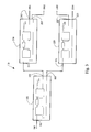
- Fig. 1 shows a frequency diplexer 10 as known according to the prior art.
- a frequency diplexer has one input port 11 and two output ports 12 and 13. It comprises two directional couplers 14 and 15, the left one 14 on Fig. 2 being said an upstream directional coupler and the right one 15 being said a downstream directional coupler.
- Each directional coupler 14 ; 15 has one input port 14i ; 15i and three output ports generally said : a coupled port 14co ; 15co, an isolated port 14io ; 15io and a through port 14to : 15to.
- the input port 14i of the upstream directional coupler 14 acts as the input port 11 of the frequency diplexer 10.
- the isolated output port 14io of the uplink directional coupler 14 acts as the second output port 13 of the frequency diplexer 10.
- the through output port 14to of the uplink directional coupler 14 is connected to the output port 16o of a first filter 16 the input port 16i of which is connected to the input port 15i of the downstream directional coupler 15.
- the coupled output port 14co of the upstream directional coupler 14 is connected to the input port 17i of a second filter 17 the output port 17o of which is connected to the isolated output port 15io of the downstream directional coupler 15.
- the through output port 15to of the downstream directional coupler 15 is supplied by a short-circuited adapting impedance 18.
- the coupled output port 15co of the upstream directional coupler 15 acts as the first output port 12 of the frequency diplexer 10.
- the two couplers 14 and 15 of a diplexer 10 are directional couplers, for example Lange couplers. Each signal over either the through output port 14to ; 15to or the coupled output port 14co ; 15co of each directional coupler is attenuated relative to the input port by a 3dB factor and the phase difference between the signals over these two output ports is ⁇ /2.
- the two filters 16 and 17 of a frequency diplexer 10 are identical.
- the frequency diplexer 10 depicted in Fig. 1 entails a given frequency response over a first frequency range on the first output port, for example the port 12, and another frequency response over a second frequency range complementary of the first frequency range on the second output port, for example the port 13.
- the filters 16 and 17 may be band-pass filters making the frequency diplexer 10 to act as a band-pass/band reject filter (one output port 12 for the band-pass filtered signals and the other output port 13 for the band reject filtered signals). They may be band-reject still making the frequency diplexer 10 to act as a band-pass/band reject filter. They may be high-pass or low-pass filters making the frequency diplexer 10 to act as a low-pass/high-reject filter.
- said frequency diplexer comprises
- the present invention also relates to a frequency multiplexing-demultiplexing device having an input port and N output ports, said device comprises a series of N-1 diplexers, each diplexers acting as a band pass/band reject filter having a band-pass output port and a band reject output port, the band-pass output port of each diplexer being connected to an output port of said device and the band reject output port of each diplexer being connected to the input port of the following diplexer in the series of diplexers except for the last diplexer of the series, the input port of the first diplexer of the series being connected to the input port of the device, the band that a diplexer lets to pass over its band-pass output port being included inside the band that the previous diplexer lets to pass over its band-rejected output port, said diplexers being frequency diplexers according to the present invention as aforedescribed .
- the present invention also relates to a frequency multiplexing-demultiplexing device having an input port and N output ports, said device comprising a first diplexer the input port of which is connected to the input port of the device and the two output ports of which are respectively connected to the input ports of two second diplexers, the output ports of the two second diplexers are respectively connected to the four output ports of the device, the first diplexer acting as a band-pass/band-reject filter and the two second diplexers acting as low-pass/high-pass filters, said diplexers being frequency diplexers according to the present invention as aforedescribed.
- a frequency diplexer according to the invention is now described in relation with Fig. 2.
- a frequency diplexer of the prior art it has one input port 11 and two output ports 12 and 13. It comprises two directional couplers 14 and 15, each of which has one input port 14i ; 15i and three output ports : a coupled port 14co; 15co, an isolated port 14io; 15io and a through port 14to : 15to.
- the input port 14i of the upstream directional coupler 14 acts as the input port 11 of the diplexer 10 and the isolated output port 14io acts as the second output port 13 of the diplexer 10.
- the through output port 15to of the downstream directional coupler 15 is supplied by a short-circuited adapting impedance 18 and the coupled output port 15co acts as the first output port 12 of the diplexer 10.
- the through output port 14to and the coupled output port 14co of the upstream directional coupler 14 are respectively connected to two ports of a first T splitter 19, the third port of said T splitter 19 being connected to the output port 16o of a unique filter 16.
- the input port 16i of the filter 16 is connected to a first port of a second T splitter 40, the two ports of the T splitter 40 being respectively connected the input port 15i and to the isolated output port 15io of the downstream coupler 15.
- the diplexer 10 can be made up according to the microstrip technology.
- the lines between each element of the diplexer can be microstrip lines.
- Each element can be thus microstrip elements, for example, Lange directional couplers, microstrip splitters 19 and a coupled lines filter.
- a frequency diplexer according to the invention such as the frequency diplexer 10 depicted in Fig. 2 can be used in a frequency multiplexing-demultiplexing device having an input port and at least two output ports.
- a device can act as a demultiplexer dispatching electromagnetic energy from the input port toward a plurality of output ports depending on the frequency of the input signal and, conversely, can act as a multiplexer merging the electromagnetic energy from said plurality of output ports towards the input port.
- Fig. 3 shows a frequency multiplexing-demultiplexing device D according to a first embodiment of the invention. It comprises a first frequency diplexer 100 the input port 101 of which is connected to the input port DU of the device D and the two output ports 102 and 103 of which are respectively connected to the input ports 211 and 221 of two second frequency diplexers 210 and 220. Since the multiplexing-demultiplexing device depicted in Fig. 3 is a four output ports device, the output ports 212, 213 ; 222, 223 of the two second diplexers 210 and 220 are respectively connected to the four output ports DS 1 to DS4 of the device D.
- the first diplexer 100 generally acts as a band-pass/band-reject filter with an output port, for example port 102, for the band-pass filtered signals and another output port, for example port 103, for the band-rejected signals.
- the two second diplexers 210 and 220 they act as low-pass/high-pass filters with an output port, for example ports 212 ; 222 for the low-pass filtered signals and another port, for example ports 213 ; 223, for the high-pass filtered signals.
- First and second diplexers 100, 210 and 220 generally have the same structure which is depicted in Fig. 2 and which can be seen in thin lines inside the respective diplexers on Fig. 3. They accommodate only one filter, the filter of the diplexer 100 being either a band-pass filter or a band-reject filter, the filter of the diplexers 210 and 220 being either low-pass filters or high-pass filters.
- Fig. 5a The resulting bands are given in Fig. 5a along with the reference of the ports of the concerned diplexers over which the bands appear. Thin lines represent the responses of the involved filters. Note that for obtaining the cutoff frequencies of 3.1 GHz and 4.1 GHz, low-pass and high-pass filters can be needed (they are represented in dotted lines).
- the input port 11 1 of the first diplexer 10 1 in the series of diplexers constitutes the input port DU of the frequency multiplexing-demultiplexing device D according to the invention.
- Each diplexers 10n of a device D according to the invention act as band-pass/band-reject filters, i.e. it has an output port 12n for the band-pass filtered signals (the corresponding output port 12n is now said the band-pass output port) and the other output port 13n for the band rejected signals (the corresponding output port 13n is now said the band-reject output port).
- the filter of each diplexers 10n referred as to 16 in Fig. 2 is either a band-pass filter or a band-reject filter.
- the band-pass output port will be the port 13n and the band-reject output port will be the port 12n and, in Fig. 4, the two ports 12n and 13n have to be exchanged.
- the band-pass output port 12n for the band-pass filtered signals of a diplexer 10n constitutes an output port DSn of the device D and the band-reject output port 13n for the band-rejected signals of a diplexer 10n is connected to the input port 11 n+ of the following diplexer 10n+1 in the series of diplexers, except for the last one 10 N which constitutes the last output port DSN of the device D.
- the band that a diplexer 10n lets to pass over its band-pass output port 12n for the band-pass filtered signals is included inside the band that the previous diplexer 10n-1 lets to pass over its band-reject output port 13n-1 for the band-rejected signals.
- the bands over the output ports DS1, DS2, DS3 and DS4 do not overlap.
- a frequency multiplexing-demultiplexing device requires filters having fewer order that the frequency multiplexing-demultiplexing devices of the previous embodiment such the one depicted on Fig. 2.
- Another advantage of the invention compared with the previous embodiment resides in the fact that the bandwidths of all the required filters are identical and equal to the width between two consecutive bands whereas for the filters of the devices of the previous embodiment, the bandwidth of the filters of an input diplexer is generally twice of the bandwidths of its output filters, the bandwidth of the most output filters being equal to the width between two consecutive bands. Since the lower the bandwidth is the lower the order of a filter is and since the device of the present embodiment has no filter that presents a bandwidth larger than the one of another filter, this embodiment entails a lower complexity than the one of the afore-described devices.
- elliptic filters can be used.
- the orders of the filters are respectively 5 for the band-pass filters and 7 for the low-pass or high-pass filters
- the order of all the filters falls down to 3.
Abstract
- two directional couplers (14 and 15),
- an unique filter (16) that entails either a first or a second frequency response, and,
- a first and a second T splitters (19, 40).
Description
- The present invention concerns a frequency diplexer having on a first output port a given frequency response over a first frequency range and on a second output port another frequency response over a second frequency range complementary of the first frequency range. For example, a frequency diplexer according to the invention acts as a band-pass/band-reject filter having a first output port for the band-pass filtered signals and a second output port for the band-rejected signals. Moreover, such frequency diplexer is made up in the microwave technology, for instance in the microstrip technology.
- Although the following description uses the terms "input" and "output" that could make it to be the description of devices in which the signals propagate only from an input port to an output port, it must be understood that it not the case, said devices of the present invention are intended to work either in a direction (the signals propagate from an input port to an output port) or in the other direction (the signals propagate from an output port to an input port).
- Fig. 1 shows a
frequency diplexer 10 as known according to the prior art. Such a frequency diplexer has oneinput port 11 and twooutput ports directional couplers directional coupler 14 ; 15 has oneinput port 14i ; 15i and three output ports generally said : a coupled port 14co ; 15co, an isolated port 14io ; 15io and a through port 14to : 15to. Theinput port 14i of the upstreamdirectional coupler 14 acts as theinput port 11 of thefrequency diplexer 10. The isolated output port 14io of the uplinkdirectional coupler 14 acts as thesecond output port 13 of thefrequency diplexer 10. The through output port 14to of the uplinkdirectional coupler 14 is connected to the output port 16o of afirst filter 16 the input port 16i of which is connected to theinput port 15i of the downstreamdirectional coupler 15. The coupled output port 14co of the upstreamdirectional coupler 14 is connected to the input port 17i of asecond filter 17 the output port 17o of which is connected to the isolated output port 15io of the downstreamdirectional coupler 15. The through output port 15to of the downstreamdirectional coupler 15 is supplied by a short-circuitedadapting impedance 18. The coupled output port 15co of the upstreamdirectional coupler 15 acts as thefirst output port 12 of thefrequency diplexer 10. - The two
couplers diplexer 10 are directional couplers, for example Lange couplers. Each signal over either the through output port 14to ; 15to or the coupled output port 14co ; 15co of each directional coupler is attenuated relative to the input port by a 3dB factor and the phase difference between the signals over these two output ports is π/2. - Note though the terminology used is the one of Lange couplers, it must be understood that the couplers may be of another type.
- The two
filters frequency diplexer 10 are identical. Thefrequency diplexer 10 depicted in Fig. 1 entails a given frequency response over a first frequency range on the first output port, for example theport 12, and another frequency response over a second frequency range complementary of the first frequency range on the second output port, for example theport 13. Thefilters frequency diplexer 10 to act as a band-pass/band reject filter (oneoutput port 12 for the band-pass filtered signals and theother output port 13 for the band reject filtered signals). They may be band-reject still making thefrequency diplexer 10 to act as a band-pass/band reject filter. They may be high-pass or low-pass filters making thefrequency diplexer 10 to act as a low-pass/high-reject filter. - In order to efficiently work, such a diplexer needs to have its two filters to be accurately matched, this matching turning out to be a tricky task that generally finds solutions in an increase of the complexity of the diplexer.
- It is an aim of the present invention to on the contrary decrease the complexity of a frequency diplexer compared with a frequency diplexer of the prior art of the type depicted in Fig. 1.
- This aim is achieved by providing a frequency diplexer with an input port and a first and a second output ports, said frequency diplexer entailing on the first output port a first frequency response over a first frequency range and on a second output port another frequency response over a second frequency range complementary of the first frequency range. According to the invention, said frequency diplexer comprises
- two directional couplers, each of which has one input port, a coupled output port, an isolated output port and a through output port, the input port of the upstream directional coupler acting as the input port of the diplexer, the isolated output port of the upstream directional coupler acting as the second output port of the diplexer, the through output port of the downstream directional coupler being supplied by a short-circuited adapting impedance and the coupled output port acting as the first output port of the diplexer, and
- an unique filter that entails either the first or the second frequency response, and a first and a second T splitters, the through output port and the coupled output port of the upstream directional coupler being respectively connected to the two ports of the first T splitter the third port of which is connected to the output port of the filter the input port of which is connected to a first port of the second T splitter, the two ports of the second T splitter being respectively connected the input port and to the isolated output port of the downstream coupler.
- The present invention also relates to a frequency multiplexing-demultiplexing device having an input port and N output ports, said device comprises a series of N-1 diplexers, each diplexers acting as a band pass/band reject filter having a band-pass output port and a band reject output port,
the band-pass output port of each diplexer being connected to an output port of said device and the band reject output port of each diplexer being connected to the input port of the following diplexer in the series of diplexers except for the last diplexer of the series,
the input port of the first diplexer of the series being connected to the input port of the device,
the band that a diplexer lets to pass over its band-pass output port being included inside the band that the previous diplexer lets to pass over its band-rejected output port,
said diplexers being frequency diplexers according to the present invention as aforedescribed . - The present invention also relates to a frequency multiplexing-demultiplexing device having an input port and N output ports, said device comprising a first diplexer the input port of which is connected to the input port of the device and the two output ports of which are respectively connected to the input ports of two second diplexers, the output ports of the two second diplexers are respectively connected to the four output ports of the device, the first diplexer acting as a band-pass/band-reject filter and the two second diplexers acting as low-pass/high-pass filters, said diplexers being frequency diplexers according to the present invention as aforedescribed.
- The characteristics of the invention mentioned above, as well as others, will emerge more clearly from a reading of the following description given in relation to the accompanying figures, amongst which :
- Fig. 1 shows the structure of a diplexer according to the prior art,
- Fig. 2 shows the structure of a diplexer according to the present invention,
- Fig. 3 shows a frequency multiplexing-demultiplexing device according to a first embodiment of the invention,
- Fig. 4 shows a frequency multiplexing-demultiplexing device according to a second embodiment of the invention, and
- Figs. 5a and 5b are views for illustrating the principles of the frequency multiplexing-demultiplexing devices of the embodiments of the present invention respectively shown in Figs. 3 and 4.
- A frequency diplexer according to the invention is now described in relation with Fig. 2. As a frequency diplexer of the prior art, it has one
input port 11 and twooutput ports directional couplers input port 14i ; 15i and three output ports : a coupled port 14co; 15co, an isolated port 14io; 15io and a through port 14to : 15to. Theinput port 14i of the upstreamdirectional coupler 14 acts as theinput port 11 of thediplexer 10 and the isolated output port 14io acts as thesecond output port 13 of thediplexer 10. The through output port 15to of the downstreamdirectional coupler 15 is supplied by a short-circuitedadapting impedance 18 and the coupled output port 15co acts as thefirst output port 12 of thediplexer 10. - According to the invention, the through output port 14to and the coupled output port 14co of the upstream
directional coupler 14 are respectively connected to two ports of afirst T splitter 19, the third port of saidT splitter 19 being connected to the output port 16o of aunique filter 16. The input port 16i of thefilter 16 is connected to a first port of asecond T splitter 40, the two ports of theT splitter 40 being respectively connected theinput port 15i and to the isolated output port 15io of thedownstream coupler 15. - It is understood that the use of a
unique filter 16 and of twoT splitters - The
diplexer 10 can be made up according to the microstrip technology. Thus, the lines between each element of the diplexer can be microstrip lines. Each element can be thus microstrip elements, for example, Lange directional couplers,microstrip splitters 19 and a coupled lines filter. - A frequency diplexer according to the invention such as the
frequency diplexer 10 depicted in Fig. 2 can be used in a frequency multiplexing-demultiplexing device having an input port and at least two output ports. Such a device can act as a demultiplexer dispatching electromagnetic energy from the input port toward a plurality of output ports depending on the frequency of the input signal and, conversely, can act as a multiplexer merging the electromagnetic energy from said plurality of output ports towards the input port. - Fig. 3 shows a frequency multiplexing-demultiplexing device D according to a first embodiment of the invention. It comprises a
first frequency diplexer 100 theinput port 101 of which is connected to the input port DU of the device D and the twooutput ports input ports second frequency diplexers output ports second diplexers first diplexer 100 generally acts as a band-pass/band-reject filter with an output port, forexample port 102, for the band-pass filtered signals and another output port, forexample port 103, for the band-rejected signals. As for the twosecond diplexers example ports 212 ; 222 for the low-pass filtered signals and another port, forexample ports 213 ; 223, for the high-pass filtered signals. - First and
second diplexers diplexer 100 being either a band-pass filter or a band-reject filter, the filter of thediplexers - Characteristics of a frequency multiplexing-demultiplexing device according to the first embodiment of the invention as described in relation with Fig. 2 are given in the table I below.
TABLE I Diplexer Cutoff frequencies Filter type Order 100 3.35 GHz - 3.85 GHz Band-pass ; Chebyshev 8 210 3.6 GHz Low-pass ; Chebyshev 20 220 3.6 GHZ High-pass ; Chebyshev 20 - The resulting bands are given in Fig. 5a along with the reference of the ports of the concerned diplexers over which the bands appear. Thin lines represent the responses of the involved filters. Note that for obtaining the cutoff frequencies of 3.1 GHz and 4.1 GHz, low-pass and high-pass filters can be needed (they are represented in dotted lines).
- Another embodiment of a frequency multiplexing-demultiplexing device D according to the invention is now described in relation with Fig. 4, this embodiment enabling the use of filters that have lower orders than the orders of the filters of the previous embodiment.
- The frequency multiplexing-demultiplexing device D has N output ports (in Fig. 4, N = 4). Generally speaking, such a device D comprises a series of
diplexers 101 to 10N-1 (here 101 to 103) that are cascaded; i.e. anoutput port 13i of a diplexer 10n (n = 1, 2, ..., N-2) is connected to the input port 11n+1 of the following diplexer 10n+1 in the series of diplexers. More particularly in Fig. 3, theoutput port 131 of thediplexer 101 is connected to theinput port 112 of thediplexer 102 and theoutput port 132 of thediplexer 102 is connected to theinput port 113 of thediplexer 103. Theinput port 111 of thefirst diplexer 101 in the series of diplexers constitutes the input port DU of the frequency multiplexing-demultiplexing device D according to the invention. Theoutput port 12i of each of the respective diplexers 10n (n = 1 to N-1) constitutes the output ports DSi of the device D. Theoutput port 13N-1 of thelast diplexer 10N-1 in the series of diplexers constitutes the output port DSN of the device D (in Fig. 4, N = 4). - Each diplexer 10n (n = 1 to N-1) presents the structure that is depicted in Fig. 2. However, some precisions have to be brought when considering the present embodiment. Each diplexers 10n of a device D according to the invention act as band-pass/band-reject filters, i.e. it has an output port 12n for the band-pass filtered signals (the corresponding output port 12n is now said the band-pass output port) and the other output port 13n for the band rejected signals (the corresponding output port 13n is now said the band-reject output port). For this purpose, the filter of each diplexers 10n referred as to 16 in Fig. 2 is either a band-pass filter or a band-reject filter.
- Note that if the
filter 16 is a notch filter or a band-reject filter, the band-pass output port will be the port 13n and the band-reject output port will be the port 12n and, in Fig. 4, the two ports 12n and 13n have to be exchanged. - According to the invention, the band-pass output port 12n for the band-pass filtered signals of a diplexer 10n constitutes an output port DSn of the device D and the band-reject output port 13n for the band-rejected signals of a diplexer 10n is connected to the
input port 11 n+ of the following diplexer 10n+1 in the series of diplexers, except for thelast one 10N which constitutes the last output port DSN of the device D. - According to the invention, the band that a diplexer 10n lets to pass over its band-pass output port 12n for the band-pass filtered signals is included inside the band that the previous diplexer 10n-1 lets to pass over its band-reject output port 13n-1 for the band-rejected signals.
- According to the invention, the bands over the output ports DS1, DS2, DS3 and DS4 do not overlap.
- Since for a same order of the filter, a band-pass filter or a notch filter presents a more abrupt attenuation in function of the frequency than a high-pass or low-pass filter, for a same non-overlapping behaviour of the bands, a frequency multiplexing-demultiplexing device according to that embodiment of the invention requires filters having fewer order that the frequency multiplexing-demultiplexing devices of the previous embodiment such the one depicted on Fig. 2.
- Another advantage of the invention compared with the previous embodiment resides in the fact that the bandwidths of all the required filters are identical and equal to the width between two consecutive bands whereas for the filters of the devices of the previous embodiment, the bandwidth of the filters of an input diplexer is generally twice of the bandwidths of its output filters, the bandwidth of the most output filters being equal to the width between two consecutive bands. Since the lower the bandwidth is the lower the order of a filter is and since the device of the present embodiment has no filter that presents a bandwidth larger than the one of another filter, this embodiment entails a lower complexity than the one of the afore-described devices.
- Characteristics of a frequency multiplexing-demultiplexing device according to the second embodiment described in relation with Fig. 4 are given in the table II below.
TABLE II Diplexer Cutoff frequencies Filter type Order 101 3.1 GHz- 3.35 GHz Band-pass ; Chebyshev 5 102 3.4 GHz - 3.6 GHz Band-pass ; Chebyshev 5 103 3.65 GHz - 3.85 GHz Band-pass ; Chebyshev 5 - Instead of Chebyshev filters, elliptic filters can be used. Whereas for a frequency multiplexing-demultiplexing device according to the prior art, the orders of the filters are respectively 5 for the band-pass filters and 7 for the low-pass or high-pass filters, for a frequency multiplexing-demultiplexing device according to the invention, the order of all the filters falls down to 3.
Claims (3)
- Frequency diplexer with an input port and a first and a second output ports, said frequency diplexer entailing on the first output port a first frequency response over a first frequency range and on a second output port another frequency response over a second frequency range complementary of the first frequency range, said frequency diplexer comprising- two directional couplers (14 and 15), each of which has one input port (14i ; 15i), a coupled output port (14co ; 15co), an isolated output port (14io ; 15io) and a through output port (14co; 15co), the input port (14i) of the upstream directional coupler (14) acting as the input port (11) of the diplexer, the isolated output port (14io) of the upstream directional coupler (14) acting as the second output port (13) of the diplexer, the through output port (15to) of the downstream directional coupler (15) being supplied by a short-circuited adapting impedance (18) and the coupled output port (15co) acting as the first output port (12) of the diplexer, characterized in that it further comprises :- an unique filter (16) that entails either the first or the second frequency response, and a first and a second T splitters (19, 40), the through output port (14to) and the coupled output port (14co) of the upstream directional coupler (14) being respectively connected to the two ports of the first T splitter (19) the third port of which is connected to the output port (16o) of the filter (16) the input port (16i) of which is connected to a first port of the second T splitter (40), the two ports of the second T splitter (40) being respectively connected the input port (15i) and to the isolated output port (15io) of the downstream coupler (15).
- Frequency multiplexing-demultiplexing device having an input port and N output ports (DS1 to DSN), said device comprises a series of N-1 diplexers, each diplexers (10n) acting as a band pass/band reject filter having a band-pass output port (12n) and a band reject output port (13n),
the band-pass output port (12n) of each diplexer (10n) being connected to an output port (DSn) of said device and the band reject output port (13n) of each diplexer (10n) being connected to the input port (11n+1) of the following diplexer (10n+1) in the series of diplexers except for the last diplexer (10N) of the series,
the input port (111) of the first diplexer (101) of the series being connected to the input port (DU) of the device,
the band that a diplexer (10n) lets to pass over its band-pass output port (12n) being included inside the band that the previous diplexer (10n-1) lets to pass over its band-rejected output port (13n-1),
characterized in that said diplexers (10n) are frequency diplexers according to claim 1. - Frequency multiplexing-demultiplexing device having an input port and N output ports (DS1 to DSN), said device comprising a first diplexer (100) the input port (101) of which is connected to the input port (DU) of the device (D) and the two output ports (102 and 103) of which are respectively connected to the input ports (211 and 221) of two second diplexers (210 and 220), the output ports (212, 213 ; 222, 223) of the two second diplexers (210 and 220) are respectively connected to the four output ports (DS1 to DS4) of the device (D), the first diplexer (100) acting as a band-pass/band-reject filter and the two second diplexers (210 and 220) acting as low-pass/high-pass filters.
characterized in that said diplexers (10n) are frequency diplexers according to claim 1.
Priority Applications (5)
| Application Number | Priority Date | Filing Date | Title |
|---|---|---|---|
| AT05292300T ATE421778T1 (en) | 2005-10-28 | 2005-10-28 | FREQUENCY DIPLEXER WITH ONE INPUT AND FIRST AND SECOND OUTPUTS. |
| EP05292300A EP1780828B1 (en) | 2005-10-28 | 2005-10-28 | Frequency diplexer with an input port and a first and a second output ports |
| DE602005012518T DE602005012518D1 (en) | 2005-10-28 | 2005-10-28 | Frequency diplexer with one input and first and second output. |
| US11/580,182 US7538634B2 (en) | 2005-10-28 | 2006-10-13 | Frequency diplexer with an input port and a first and a second output ports |
| JP2006294496A JP2007151101A (en) | 2005-10-28 | 2006-10-30 | Frequency diplexer and frequency multiplexing-demultiplexing device |
Applications Claiming Priority (1)
| Application Number | Priority Date | Filing Date | Title |
|---|---|---|---|
| EP05292300A EP1780828B1 (en) | 2005-10-28 | 2005-10-28 | Frequency diplexer with an input port and a first and a second output ports |
Publications (2)
| Publication Number | Publication Date |
|---|---|
| EP1780828A1 true EP1780828A1 (en) | 2007-05-02 |
| EP1780828B1 EP1780828B1 (en) | 2009-01-21 |
Family
ID=35951844
Family Applications (1)
| Application Number | Title | Priority Date | Filing Date |
|---|---|---|---|
| EP05292300A Not-in-force EP1780828B1 (en) | 2005-10-28 | 2005-10-28 | Frequency diplexer with an input port and a first and a second output ports |
Country Status (5)
| Country | Link |
|---|---|
| US (1) | US7538634B2 (en) |
| EP (1) | EP1780828B1 (en) |
| JP (1) | JP2007151101A (en) |
| AT (1) | ATE421778T1 (en) |
| DE (1) | DE602005012518D1 (en) |
Cited By (2)
| Publication number | Priority date | Publication date | Assignee | Title |
|---|---|---|---|---|
| FR2970816A1 (en) * | 2011-01-24 | 2012-07-27 | St Microelectronics Sa | RADIOFREQUENCY COMBINER |
| FR2970817A1 (en) * | 2011-01-24 | 2012-07-27 | St Microelectronics Sa | RADIOFREQUENCY SEPARATOR |
Families Citing this family (6)
| Publication number | Priority date | Publication date | Assignee | Title |
|---|---|---|---|---|
| CN101171747B (en) * | 2005-05-11 | 2010-10-27 | 艾利森电话股份有限公司 | A filter combiner |
| KR101321966B1 (en) * | 2006-12-04 | 2013-10-25 | 톰슨 라이센싱 | Tuning device with diplexer input |
| US20090102579A1 (en) * | 2006-12-29 | 2009-04-23 | Broadcom Corporation | Frequency division coupling circuit and applications thereof |
| GB2507668B (en) * | 2012-12-07 | 2014-11-05 | Radio Design Ltd | Apparatus for allowing radio frequency selectivity and method of use thereof |
| CN109196784B (en) | 2016-05-27 | 2020-07-28 | 株式会社村田制作所 | Multiplexer, high-frequency front-end circuit and communication device |
| US10043136B1 (en) * | 2017-10-12 | 2018-08-07 | International Business Machines Corporation | Reducing the number of input lines to superconducting quantum processors installed inside dilution refrigerators |
Citations (3)
| Publication number | Priority date | Publication date | Assignee | Title |
|---|---|---|---|---|
| US5058198A (en) * | 1989-03-31 | 1991-10-15 | Am Communications, Inc. | Radio frequency tap unit which can be reconfigured with minimal disruption of service |
| US5155724A (en) * | 1990-09-26 | 1992-10-13 | Rockwell International Corporation | Dual mode diplexer/multiplexer |
| US6020795A (en) * | 1997-05-19 | 2000-02-01 | Samsung Electronics Co., Ltd | Electrically controllable impedance matching device for use in RF amplifier |
Family Cites Families (2)
| Publication number | Priority date | Publication date | Assignee | Title |
|---|---|---|---|---|
| US4240155A (en) * | 1978-06-28 | 1980-12-16 | Micro Communications, Inc. | Diplexer and multiplexer |
| US6278498B1 (en) * | 1998-04-01 | 2001-08-21 | Adc Telecommunications, Inc. | Apparatus and method for combining digital and analog television signals |
-
2005
- 2005-10-28 DE DE602005012518T patent/DE602005012518D1/en not_active Expired - Fee Related
- 2005-10-28 EP EP05292300A patent/EP1780828B1/en not_active Not-in-force
- 2005-10-28 AT AT05292300T patent/ATE421778T1/en not_active IP Right Cessation
-
2006
- 2006-10-13 US US11/580,182 patent/US7538634B2/en not_active Expired - Fee Related
- 2006-10-30 JP JP2006294496A patent/JP2007151101A/en active Pending
Patent Citations (3)
| Publication number | Priority date | Publication date | Assignee | Title |
|---|---|---|---|---|
| US5058198A (en) * | 1989-03-31 | 1991-10-15 | Am Communications, Inc. | Radio frequency tap unit which can be reconfigured with minimal disruption of service |
| US5155724A (en) * | 1990-09-26 | 1992-10-13 | Rockwell International Corporation | Dual mode diplexer/multiplexer |
| US6020795A (en) * | 1997-05-19 | 2000-02-01 | Samsung Electronics Co., Ltd | Electrically controllable impedance matching device for use in RF amplifier |
Cited By (6)
| Publication number | Priority date | Publication date | Assignee | Title |
|---|---|---|---|---|
| FR2970816A1 (en) * | 2011-01-24 | 2012-07-27 | St Microelectronics Sa | RADIOFREQUENCY COMBINER |
| FR2970817A1 (en) * | 2011-01-24 | 2012-07-27 | St Microelectronics Sa | RADIOFREQUENCY SEPARATOR |
| US8712466B2 (en) | 2011-01-24 | 2014-04-29 | Stmicroelectronics Sa | Radio frequency splitter |
| US8843087B2 (en) | 2011-01-24 | 2014-09-23 | Stmicroelectronics Sa | Radio frequency combiner |
| US9231642B2 (en) | 2011-01-24 | 2016-01-05 | Stmicroelectronics Sa | Radio frequency splitter |
| US9853345B2 (en) | 2011-01-24 | 2017-12-26 | Stmicroelectronics Sa | Radio frequency splitter |
Also Published As
| Publication number | Publication date |
|---|---|
| US7538634B2 (en) | 2009-05-26 |
| EP1780828B1 (en) | 2009-01-21 |
| DE602005012518D1 (en) | 2009-03-12 |
| JP2007151101A (en) | 2007-06-14 |
| US20070096846A1 (en) | 2007-05-03 |
| ATE421778T1 (en) | 2009-02-15 |
Similar Documents
| Publication | Publication Date | Title |
|---|---|---|
| EP1780828B1 (en) | Frequency diplexer with an input port and a first and a second output ports | |
| JP5493002B2 (en) | Radio frequency filter | |
| US4423396A (en) | Bandpass filter for UHF band | |
| US10270148B2 (en) | Microstrip multiplexer | |
| US6958663B2 (en) | In-band group delay equalizer and distortion compensation amplifier | |
| CN110931923A (en) | Microstrip continuous passband broadband duplexer based on multiple broadband bridges and bandpass filters | |
| US7948332B2 (en) | N-channel multiplexer | |
| US8228135B2 (en) | Band combining filter | |
| US4433314A (en) | Millimeter wave suspended substrate multiplexer | |
| TWI672857B (en) | Power distributing device | |
| EP3172842B1 (en) | Radio frequency multiplexer and receiver filter | |
| CN114497932B (en) | Millimeter wave duplexer inserted with EBG structure | |
| US3426292A (en) | Phase-coherent band-splitting and recombination network | |
| KR100998603B1 (en) | Dual-band filter and method for designing the same | |
| US20080143456A1 (en) | Band combining filter | |
| KR100763582B1 (en) | Compact wave-guide filter | |
| US9755287B2 (en) | Frequency demultiplexer | |
| GB2444786A (en) | Band combining filter | |
| JP7076540B2 (en) | Electrical filter structure | |
| CN211238450U (en) | Microstrip continuous passband broadband duplexer | |
| US3543188A (en) | Microwave diplexing technique employing predistorted waveguide filters | |
| KR101367310B1 (en) | Wideband planar 3 db branch line coupler improving selectivity | |
| GB2306792A (en) | Microwave multiplexer | |
| JPH01286601A (en) | Microwave band branching filter | |
| US20230147406A1 (en) | AU and RU having CWG Filters, and BS having the AU or RU |
Legal Events
| Date | Code | Title | Description |
|---|---|---|---|
| PUAI | Public reference made under article 153(3) epc to a published international application that has entered the european phase |
Free format text: ORIGINAL CODE: 0009012 |
|
| AK | Designated contracting states |
Kind code of ref document: A1 Designated state(s): AT BE BG CH CY CZ DE DK EE ES FI FR GB GR HU IE IS IT LI LT LU LV MC NL PL PT RO SE SI SK TR |
|
| AX | Request for extension of the european patent |
Extension state: AL BA HR MK YU |
|
| 17P | Request for examination filed |
Effective date: 20070625 |
|
| 17Q | First examination report despatched |
Effective date: 20070806 |
|
| AKX | Designation fees paid |
Designated state(s): AT BE BG CH CY CZ DE DK EE ES FI FR GB GR HU IE IS IT LI LT LU LV MC NL PL PT RO SE SI SK TR |
|
| GRAP | Despatch of communication of intention to grant a patent |
Free format text: ORIGINAL CODE: EPIDOSNIGR1 |
|
| GRAS | Grant fee paid |
Free format text: ORIGINAL CODE: EPIDOSNIGR3 |
|
| GRAA | (expected) grant |
Free format text: ORIGINAL CODE: 0009210 |
|
| STAA | Information on the status of an ep patent application or granted ep patent |
Free format text: STATUS: THE PATENT HAS BEEN GRANTED |
|
| AK | Designated contracting states |
Kind code of ref document: B1 Designated state(s): AT BE BG CH CY CZ DE DK EE ES FI FR GB GR HU IE IS IT LI LT LU LV MC NL PL PT RO SE SI SK TR |
|
| REG | Reference to a national code |
Ref country code: GB Ref legal event code: FG4D |
|
| REG | Reference to a national code |
Ref country code: CH Ref legal event code: EP |
|
| REG | Reference to a national code |
Ref country code: IE Ref legal event code: FG4D |
|
| REF | Corresponds to: |
Ref document number: 602005012518 Country of ref document: DE Date of ref document: 20090312 Kind code of ref document: P |
|
| PG25 | Lapsed in a contracting state [announced via postgrant information from national office to epo] |
Ref country code: NL Free format text: LAPSE BECAUSE OF FAILURE TO SUBMIT A TRANSLATION OF THE DESCRIPTION OR TO PAY THE FEE WITHIN THE PRESCRIBED TIME-LIMIT Effective date: 20090121 |
|
| NLV1 | Nl: lapsed or annulled due to failure to fulfill the requirements of art. 29p and 29m of the patents act | ||
| PG25 | Lapsed in a contracting state [announced via postgrant information from national office to epo] |
Ref country code: SI Free format text: LAPSE BECAUSE OF FAILURE TO SUBMIT A TRANSLATION OF THE DESCRIPTION OR TO PAY THE FEE WITHIN THE PRESCRIBED TIME-LIMIT Effective date: 20090121 Ref country code: LT Free format text: LAPSE BECAUSE OF FAILURE TO SUBMIT A TRANSLATION OF THE DESCRIPTION OR TO PAY THE FEE WITHIN THE PRESCRIBED TIME-LIMIT Effective date: 20090121 Ref country code: FI Free format text: LAPSE BECAUSE OF FAILURE TO SUBMIT A TRANSLATION OF THE DESCRIPTION OR TO PAY THE FEE WITHIN THE PRESCRIBED TIME-LIMIT Effective date: 20090121 Ref country code: ES Free format text: LAPSE BECAUSE OF FAILURE TO SUBMIT A TRANSLATION OF THE DESCRIPTION OR TO PAY THE FEE WITHIN THE PRESCRIBED TIME-LIMIT Effective date: 20090502 |
|
| PG25 | Lapsed in a contracting state [announced via postgrant information from national office to epo] |
Ref country code: SE Free format text: LAPSE BECAUSE OF FAILURE TO SUBMIT A TRANSLATION OF THE DESCRIPTION OR TO PAY THE FEE WITHIN THE PRESCRIBED TIME-LIMIT Effective date: 20090421 Ref country code: PT Free format text: LAPSE BECAUSE OF FAILURE TO SUBMIT A TRANSLATION OF THE DESCRIPTION OR TO PAY THE FEE WITHIN THE PRESCRIBED TIME-LIMIT Effective date: 20090622 Ref country code: LV Free format text: LAPSE BECAUSE OF FAILURE TO SUBMIT A TRANSLATION OF THE DESCRIPTION OR TO PAY THE FEE WITHIN THE PRESCRIBED TIME-LIMIT Effective date: 20090121 Ref country code: PL Free format text: LAPSE BECAUSE OF FAILURE TO SUBMIT A TRANSLATION OF THE DESCRIPTION OR TO PAY THE FEE WITHIN THE PRESCRIBED TIME-LIMIT Effective date: 20090121 Ref country code: AT Free format text: LAPSE BECAUSE OF FAILURE TO SUBMIT A TRANSLATION OF THE DESCRIPTION OR TO PAY THE FEE WITHIN THE PRESCRIBED TIME-LIMIT Effective date: 20090121 Ref country code: IS Free format text: LAPSE BECAUSE OF FAILURE TO SUBMIT A TRANSLATION OF THE DESCRIPTION OR TO PAY THE FEE WITHIN THE PRESCRIBED TIME-LIMIT Effective date: 20090521 |
|
| PG25 | Lapsed in a contracting state [announced via postgrant information from national office to epo] |
Ref country code: BE Free format text: LAPSE BECAUSE OF FAILURE TO SUBMIT A TRANSLATION OF THE DESCRIPTION OR TO PAY THE FEE WITHIN THE PRESCRIBED TIME-LIMIT Effective date: 20090121 |
|
| PG25 | Lapsed in a contracting state [announced via postgrant information from national office to epo] |
Ref country code: DK Free format text: LAPSE BECAUSE OF FAILURE TO SUBMIT A TRANSLATION OF THE DESCRIPTION OR TO PAY THE FEE WITHIN THE PRESCRIBED TIME-LIMIT Effective date: 20090121 Ref country code: CZ Free format text: LAPSE BECAUSE OF FAILURE TO SUBMIT A TRANSLATION OF THE DESCRIPTION OR TO PAY THE FEE WITHIN THE PRESCRIBED TIME-LIMIT Effective date: 20090121 Ref country code: EE Free format text: LAPSE BECAUSE OF FAILURE TO SUBMIT A TRANSLATION OF THE DESCRIPTION OR TO PAY THE FEE WITHIN THE PRESCRIBED TIME-LIMIT Effective date: 20090121 |
|
| PLBE | No opposition filed within time limit |
Free format text: ORIGINAL CODE: 0009261 |
|
| STAA | Information on the status of an ep patent application or granted ep patent |
Free format text: STATUS: NO OPPOSITION FILED WITHIN TIME LIMIT |
|
| PG25 | Lapsed in a contracting state [announced via postgrant information from national office to epo] |
Ref country code: SK Free format text: LAPSE BECAUSE OF FAILURE TO SUBMIT A TRANSLATION OF THE DESCRIPTION OR TO PAY THE FEE WITHIN THE PRESCRIBED TIME-LIMIT Effective date: 20090121 Ref country code: RO Free format text: LAPSE BECAUSE OF FAILURE TO SUBMIT A TRANSLATION OF THE DESCRIPTION OR TO PAY THE FEE WITHIN THE PRESCRIBED TIME-LIMIT Effective date: 20090121 |
|
| 26N | No opposition filed |
Effective date: 20091022 |
|
| PG25 | Lapsed in a contracting state [announced via postgrant information from national office to epo] |
Ref country code: BG Free format text: LAPSE BECAUSE OF FAILURE TO SUBMIT A TRANSLATION OF THE DESCRIPTION OR TO PAY THE FEE WITHIN THE PRESCRIBED TIME-LIMIT Effective date: 20090421 |
|
| PG25 | Lapsed in a contracting state [announced via postgrant information from national office to epo] |
Ref country code: MC Free format text: LAPSE BECAUSE OF NON-PAYMENT OF DUE FEES Effective date: 20091031 |
|
| REG | Reference to a national code |
Ref country code: CH Ref legal event code: PL |
|
| REG | Reference to a national code |
Ref country code: IE Ref legal event code: MM4A |
|
| REG | Reference to a national code |
Ref country code: FR Ref legal event code: ST Effective date: 20100630 |
|
| PG25 | Lapsed in a contracting state [announced via postgrant information from national office to epo] |
Ref country code: DE Free format text: LAPSE BECAUSE OF NON-PAYMENT OF DUE FEES Effective date: 20100501 Ref country code: FR Free format text: LAPSE BECAUSE OF NON-PAYMENT OF DUE FEES Effective date: 20091102 |
|
| PG25 | Lapsed in a contracting state [announced via postgrant information from national office to epo] |
Ref country code: LI Free format text: LAPSE BECAUSE OF NON-PAYMENT OF DUE FEES Effective date: 20091031 Ref country code: IE Free format text: LAPSE BECAUSE OF NON-PAYMENT OF DUE FEES Effective date: 20091028 Ref country code: GR Free format text: LAPSE BECAUSE OF FAILURE TO SUBMIT A TRANSLATION OF THE DESCRIPTION OR TO PAY THE FEE WITHIN THE PRESCRIBED TIME-LIMIT Effective date: 20090422 Ref country code: CH Free format text: LAPSE BECAUSE OF NON-PAYMENT OF DUE FEES Effective date: 20091031 |
|
| PG25 | Lapsed in a contracting state [announced via postgrant information from national office to epo] |
Ref country code: GB Free format text: LAPSE BECAUSE OF NON-PAYMENT OF DUE FEES Effective date: 20091028 |
|
| PG25 | Lapsed in a contracting state [announced via postgrant information from national office to epo] |
Ref country code: IT Free format text: LAPSE BECAUSE OF FAILURE TO SUBMIT A TRANSLATION OF THE DESCRIPTION OR TO PAY THE FEE WITHIN THE PRESCRIBED TIME-LIMIT Effective date: 20090121 |
|
| PG25 | Lapsed in a contracting state [announced via postgrant information from national office to epo] |
Ref country code: LU Free format text: LAPSE BECAUSE OF NON-PAYMENT OF DUE FEES Effective date: 20091028 |
|
| PG25 | Lapsed in a contracting state [announced via postgrant information from national office to epo] |
Ref country code: HU Free format text: LAPSE BECAUSE OF FAILURE TO SUBMIT A TRANSLATION OF THE DESCRIPTION OR TO PAY THE FEE WITHIN THE PRESCRIBED TIME-LIMIT Effective date: 20090722 |
|
| PG25 | Lapsed in a contracting state [announced via postgrant information from national office to epo] |
Ref country code: TR Free format text: LAPSE BECAUSE OF FAILURE TO SUBMIT A TRANSLATION OF THE DESCRIPTION OR TO PAY THE FEE WITHIN THE PRESCRIBED TIME-LIMIT Effective date: 20090121 |
|
| PG25 | Lapsed in a contracting state [announced via postgrant information from national office to epo] |
Ref country code: CY Free format text: LAPSE BECAUSE OF FAILURE TO SUBMIT A TRANSLATION OF THE DESCRIPTION OR TO PAY THE FEE WITHIN THE PRESCRIBED TIME-LIMIT Effective date: 20090121 |