EP1780693A2 - Plasma display appratus and method of driving the same - Google Patents
Plasma display appratus and method of driving the same Download PDFInfo
- Publication number
- EP1780693A2 EP1780693A2 EP06255586A EP06255586A EP1780693A2 EP 1780693 A2 EP1780693 A2 EP 1780693A2 EP 06255586 A EP06255586 A EP 06255586A EP 06255586 A EP06255586 A EP 06255586A EP 1780693 A2 EP1780693 A2 EP 1780693A2
- Authority
- EP
- European Patent Office
- Prior art keywords
- frame
- reset pulse
- plasma display
- video data
- variation
- Prior art date
- Legal status (The legal status is an assumption and is not a legal conclusion. Google has not performed a legal analysis and makes no representation as to the accuracy of the status listed.)
- Withdrawn
Links
Images

Classifications
-
- G—PHYSICS
- G09—EDUCATION; CRYPTOGRAPHY; DISPLAY; ADVERTISING; SEALS
- G09G—ARRANGEMENTS OR CIRCUITS FOR CONTROL OF INDICATING DEVICES USING STATIC MEANS TO PRESENT VARIABLE INFORMATION
- G09G3/00—Control arrangements or circuits, of interest only in connection with visual indicators other than cathode-ray tubes
- G09G3/20—Control arrangements or circuits, of interest only in connection with visual indicators other than cathode-ray tubes for presentation of an assembly of a number of characters, e.g. a page, by composing the assembly by combination of individual elements arranged in a matrix no fixed position being assigned to or needed to be assigned to the individual characters or partial characters
- G09G3/22—Control arrangements or circuits, of interest only in connection with visual indicators other than cathode-ray tubes for presentation of an assembly of a number of characters, e.g. a page, by composing the assembly by combination of individual elements arranged in a matrix no fixed position being assigned to or needed to be assigned to the individual characters or partial characters using controlled light sources
- G09G3/28—Control arrangements or circuits, of interest only in connection with visual indicators other than cathode-ray tubes for presentation of an assembly of a number of characters, e.g. a page, by composing the assembly by combination of individual elements arranged in a matrix no fixed position being assigned to or needed to be assigned to the individual characters or partial characters using controlled light sources using luminous gas-discharge panels, e.g. plasma panels
- G09G3/288—Control arrangements or circuits, of interest only in connection with visual indicators other than cathode-ray tubes for presentation of an assembly of a number of characters, e.g. a page, by composing the assembly by combination of individual elements arranged in a matrix no fixed position being assigned to or needed to be assigned to the individual characters or partial characters using controlled light sources using luminous gas-discharge panels, e.g. plasma panels using AC panels
- G09G3/291—Control arrangements or circuits, of interest only in connection with visual indicators other than cathode-ray tubes for presentation of an assembly of a number of characters, e.g. a page, by composing the assembly by combination of individual elements arranged in a matrix no fixed position being assigned to or needed to be assigned to the individual characters or partial characters using controlled light sources using luminous gas-discharge panels, e.g. plasma panels using AC panels controlling the gas discharge to control a cell condition, e.g. by means of specific pulse shapes
- G09G3/292—Control arrangements or circuits, of interest only in connection with visual indicators other than cathode-ray tubes for presentation of an assembly of a number of characters, e.g. a page, by composing the assembly by combination of individual elements arranged in a matrix no fixed position being assigned to or needed to be assigned to the individual characters or partial characters using controlled light sources using luminous gas-discharge panels, e.g. plasma panels using AC panels controlling the gas discharge to control a cell condition, e.g. by means of specific pulse shapes for reset discharge, priming discharge or erase discharge occurring in a phase other than addressing
- G09G3/2927—Details of initialising
-
- G—PHYSICS
- G09—EDUCATION; CRYPTOGRAPHY; DISPLAY; ADVERTISING; SEALS
- G09G—ARRANGEMENTS OR CIRCUITS FOR CONTROL OF INDICATING DEVICES USING STATIC MEANS TO PRESENT VARIABLE INFORMATION
- G09G3/00—Control arrangements or circuits, of interest only in connection with visual indicators other than cathode-ray tubes
- G09G3/20—Control arrangements or circuits, of interest only in connection with visual indicators other than cathode-ray tubes for presentation of an assembly of a number of characters, e.g. a page, by composing the assembly by combination of individual elements arranged in a matrix no fixed position being assigned to or needed to be assigned to the individual characters or partial characters
- G09G3/22—Control arrangements or circuits, of interest only in connection with visual indicators other than cathode-ray tubes for presentation of an assembly of a number of characters, e.g. a page, by composing the assembly by combination of individual elements arranged in a matrix no fixed position being assigned to or needed to be assigned to the individual characters or partial characters using controlled light sources
- G09G3/28—Control arrangements or circuits, of interest only in connection with visual indicators other than cathode-ray tubes for presentation of an assembly of a number of characters, e.g. a page, by composing the assembly by combination of individual elements arranged in a matrix no fixed position being assigned to or needed to be assigned to the individual characters or partial characters using controlled light sources using luminous gas-discharge panels, e.g. plasma panels
- G09G3/288—Control arrangements or circuits, of interest only in connection with visual indicators other than cathode-ray tubes for presentation of an assembly of a number of characters, e.g. a page, by composing the assembly by combination of individual elements arranged in a matrix no fixed position being assigned to or needed to be assigned to the individual characters or partial characters using controlled light sources using luminous gas-discharge panels, e.g. plasma panels using AC panels
- G09G3/296—Driving circuits for producing the waveforms applied to the driving electrodes
-
- G—PHYSICS
- G09—EDUCATION; CRYPTOGRAPHY; DISPLAY; ADVERTISING; SEALS
- G09G—ARRANGEMENTS OR CIRCUITS FOR CONTROL OF INDICATING DEVICES USING STATIC MEANS TO PRESENT VARIABLE INFORMATION
- G09G3/00—Control arrangements or circuits, of interest only in connection with visual indicators other than cathode-ray tubes
- G09G3/20—Control arrangements or circuits, of interest only in connection with visual indicators other than cathode-ray tubes for presentation of an assembly of a number of characters, e.g. a page, by composing the assembly by combination of individual elements arranged in a matrix no fixed position being assigned to or needed to be assigned to the individual characters or partial characters
- G09G3/2007—Display of intermediate tones
- G09G3/2018—Display of intermediate tones by time modulation using two or more time intervals
- G09G3/2022—Display of intermediate tones by time modulation using two or more time intervals using sub-frames
-
- G—PHYSICS
- G09—EDUCATION; CRYPTOGRAPHY; DISPLAY; ADVERTISING; SEALS
- G09G—ARRANGEMENTS OR CIRCUITS FOR CONTROL OF INDICATING DEVICES USING STATIC MEANS TO PRESENT VARIABLE INFORMATION
- G09G2310/00—Command of the display device
- G09G2310/06—Details of flat display driving waveforms
- G09G2310/066—Waveforms comprising a gently increasing or decreasing portion, e.g. ramp
-
- G—PHYSICS
- G09—EDUCATION; CRYPTOGRAPHY; DISPLAY; ADVERTISING; SEALS
- G09G—ARRANGEMENTS OR CIRCUITS FOR CONTROL OF INDICATING DEVICES USING STATIC MEANS TO PRESENT VARIABLE INFORMATION
- G09G2320/00—Control of display operating conditions
- G09G2320/02—Improving the quality of display appearance
- G09G2320/0228—Increasing the driving margin in plasma displays
-
- G—PHYSICS
- G09—EDUCATION; CRYPTOGRAPHY; DISPLAY; ADVERTISING; SEALS
- G09G—ARRANGEMENTS OR CIRCUITS FOR CONTROL OF INDICATING DEVICES USING STATIC MEANS TO PRESENT VARIABLE INFORMATION
- G09G2320/00—Control of display operating conditions
- G09G2320/02—Improving the quality of display appearance
- G09G2320/0233—Improving the luminance or brightness uniformity across the screen
-
- G—PHYSICS
- G09—EDUCATION; CRYPTOGRAPHY; DISPLAY; ADVERTISING; SEALS
- G09G—ARRANGEMENTS OR CIRCUITS FOR CONTROL OF INDICATING DEVICES USING STATIC MEANS TO PRESENT VARIABLE INFORMATION
- G09G2320/00—Control of display operating conditions
- G09G2320/02—Improving the quality of display appearance
- G09G2320/0238—Improving the black level
-
- G—PHYSICS
- G09—EDUCATION; CRYPTOGRAPHY; DISPLAY; ADVERTISING; SEALS
- G09G—ARRANGEMENTS OR CIRCUITS FOR CONTROL OF INDICATING DEVICES USING STATIC MEANS TO PRESENT VARIABLE INFORMATION
- G09G2330/00—Aspects of power supply; Aspects of display protection and defect management
- G09G2330/02—Details of power systems and of start or stop of display operation
- G09G2330/028—Generation of voltages supplied to electrode drivers in a matrix display other than LCD
-
- G—PHYSICS
- G09—EDUCATION; CRYPTOGRAPHY; DISPLAY; ADVERTISING; SEALS
- G09G—ARRANGEMENTS OR CIRCUITS FOR CONTROL OF INDICATING DEVICES USING STATIC MEANS TO PRESENT VARIABLE INFORMATION
- G09G2340/00—Aspects of display data processing
- G09G2340/16—Determination of a pixel data signal depending on the signal applied in the previous frame
-
- G—PHYSICS
- G09—EDUCATION; CRYPTOGRAPHY; DISPLAY; ADVERTISING; SEALS
- G09G—ARRANGEMENTS OR CIRCUITS FOR CONTROL OF INDICATING DEVICES USING STATIC MEANS TO PRESENT VARIABLE INFORMATION
- G09G2360/00—Aspects of the architecture of display systems
- G09G2360/16—Calculation or use of calculated indices related to luminance levels in display data
-
- G—PHYSICS
- G09—EDUCATION; CRYPTOGRAPHY; DISPLAY; ADVERTISING; SEALS
- G09G—ARRANGEMENTS OR CIRCUITS FOR CONTROL OF INDICATING DEVICES USING STATIC MEANS TO PRESENT VARIABLE INFORMATION
- G09G3/00—Control arrangements or circuits, of interest only in connection with visual indicators other than cathode-ray tubes
- G09G3/20—Control arrangements or circuits, of interest only in connection with visual indicators other than cathode-ray tubes for presentation of an assembly of a number of characters, e.g. a page, by composing the assembly by combination of individual elements arranged in a matrix no fixed position being assigned to or needed to be assigned to the individual characters or partial characters
- G09G3/22—Control arrangements or circuits, of interest only in connection with visual indicators other than cathode-ray tubes for presentation of an assembly of a number of characters, e.g. a page, by composing the assembly by combination of individual elements arranged in a matrix no fixed position being assigned to or needed to be assigned to the individual characters or partial characters using controlled light sources
- G09G3/28—Control arrangements or circuits, of interest only in connection with visual indicators other than cathode-ray tubes for presentation of an assembly of a number of characters, e.g. a page, by composing the assembly by combination of individual elements arranged in a matrix no fixed position being assigned to or needed to be assigned to the individual characters or partial characters using controlled light sources using luminous gas-discharge panels, e.g. plasma panels
- G09G3/288—Control arrangements or circuits, of interest only in connection with visual indicators other than cathode-ray tubes for presentation of an assembly of a number of characters, e.g. a page, by composing the assembly by combination of individual elements arranged in a matrix no fixed position being assigned to or needed to be assigned to the individual characters or partial characters using controlled light sources using luminous gas-discharge panels, e.g. plasma panels using AC panels
- G09G3/296—Driving circuits for producing the waveforms applied to the driving electrodes
- G09G3/2965—Driving circuits for producing the waveforms applied to the driving electrodes using inductors for energy recovery
Definitions
- This invention relates to a plasma display apparatus and a method of driving the same.
- a plasma display apparatus includes a plasma display panel and a driver for driving the plasma display panel.
- the driver supplies a driving pulse to the plasma display panel during a frame including a plurality of subfields such that an image is displayed on the plasma display panel.
- Each subfield includes a reset period, an address period, and a sustain period.
- the driver supplies a reset pulse for making uniform wall charges formed in all of discharge cells of the plasma display panel.
- the driver supplies a scan pulse and a data pulse for selecting discharges cells to be turned on.
- the driver supplies a sustain pulse for emitting light in the discharge cells selected during the address period.
- the present invention seeks to provide an improved plasma display apparatus and method of driving thereof
- a plasma display apparatus comprises a plasma display panel comprising an electrode, and a driver arranged to supply a second reset pulse to the electrode during a second frame when a variation between a video data load of a first frame and a video data load of the second frame is greater than a threshold value, the second reset pulse supplied during the second frame being arranged to generate a reset discharge, that is greater than a reset discharge generated by a first reset pulse supplied during the first frame.
- the ratio of the threshold value to the larger load of the video data load of the first frame and the video data load of the second frame may be equal to or greater than 0.2.
- the variation may be equal to the difference between the sum of a gray level corresponding to each subpixel in the first frame and the sum of a gray level corresponding to each subpixel in the second frame.
- the variation may be equal to the difference between the sum of an average gray level corresponding to each pixel in the first frame and the sum of an average gray level corresponding to each pixel in the second frame.
- the driver may set at least one of a rising slope or the highest voltage of the second reset pulse to be greater than at least one of a rising slope or the highest voltage of the first reset pulse.
- the driver may comprise a switch arranged to supply the first reset pulse and the second reset pulse.
- the switch may be arranged to receive a control signal having a first duty ratio, and to then supply the first reset pulse.
- the switch may be arranged to receive a control signal having a second duty ratio greater than the first duty ratio, and then to supply the second reset pulse.
- the highest voltage of the second reset pulse may be greater than the highest voltage of the first reset pulse.
- the driver may be arranged to supply the second reset pulse in at least one subfield of all of subfields of the second frame.
- the first frame and the second frame may be consecutive frames.
- the variation may be equal to the difference between the average picture level (APL) of the video data of the first frame and the APL of the video data of the second frame.
- APL average picture level
- a method of driving a plasma display apparatus comprising an electrode, comprises calculating the variation between a video data load of a first frame and video data load of a second frame, comparing the variation with a threshold value, and supplying a second reset pulse to the electrode during a second frame when the variation is greater than the threshold value, the second reset pulse supplied during the second frame generating a reset discharge, that is greater than a reset discharge generated by a first reset pulse supplied during the first frame.
- the ratio of the threshold value to the larger load of the video data load of the first frame and the video data load of the second frame may be equal to or more than 0.2.
- the variation may be equal to the difference between the sum of a gray level corresponding to each subpixel in the first frame and a sum of a gray level corresponding to each subpixel in the second frame.
- the variation may be equal to the difference between the sum of an average gray level corresponding to each pixel in the first frame and the sum of an average gray level corresponding to each pixel in the second frame.
- At least one of a rising slope or the highest voltage of the second reset pulse may be greater than at least one of a rising slope or the highest voltage of the first reset pulse.
- the first reset pulse may be supplied in response to a control signal having a first duty ratio
- the second reset pulse may be supplied in response to a control signal having a second duty ratio greater than the first duty ratio
- the highest voltage of the second reset pulse may be greater than the highest voltage of the first reset pulse.
- the second reset pulse may be supplied in at least one subfield of all of subfields of the second frame.
- the first frame and the second frame may be consecutive frames.
- the variation may be equal to the difference between the APL of the video data of the first frame and the APL of the video data of the second frame.
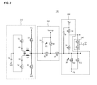
- FIG. 1 illustrates a plasma display apparatus according to an embodiment
- FIG. 2 illustrates a scan driver of the plasma display apparatus according to the embodiment
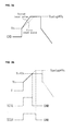
- FIGs. 3a and 3b illustrate a first reset pulse and a second reset pulse in a first frame and a second frame
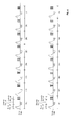
- FIG. 4 illustrates a subfield in which a second reset pulse is supplied.
- a plasma display apparatus includes a plasma display panel 100, a data variation calculator 110, a comparator 120, a control signal generator 130, a scan driver 140, an address driver 150, and a sustain driver 160.
- the plasma display panel 100 includes scan electrodes Y1 to Yn, address electrodes X1 to Xm, and sustain electrodes Z1 to Zn.
- the data variation calculator 110 calculates the variation between a load of video data input during a first frame and a load of video data input during a second frame.
- the load of the video data may be equal to the average picture level (APL) in one frame or the sum of gray levels in one frame.
- APL average picture level
- the data variation calculator 110 is capable of calculating the variation in two ways.
- the data variation calculator 110 calculates the APL of video data input during the first frame and the APL of video data input during the second frame, and then calculates the difference between the APL of the first frame and the APL of the second frame. More particularly, the data variation calculator 110 calculates the sum of gray levels corresponding to video data input during the first frame and the sum of gray levels corresponding to video data input during the second frame, and then calculates the difference between the sum of the gray levels of the first frame and the sum of the gray levels of the second frame.
- first frame and the second frame are consecutive frames: however this is not essential to the invention in its broadest aspect.
- first frame may be either an n-th frame or an n+1-th frame
- second frame may be the other frame.
- the comparator 120 compares the variation output from the data variation calculator 110 with a threshold value TH, and then outputs a discharge control signal when the variation is greater than the threshold value TH. More specifically, the comparator 120 compares the difference between the APL of the first frame and the APL of the second frame with the threshold value TH, and then outputs a discharge control signal when the difference is greater than the threshold value TH.
- the comparator 120 compares the difference between the sum of the gray levels of the first frame and the sum of the gray levels of the second frame with the threshold value TH, and then outputs a discharge control signal when the difference is greater than the threshold value TH.
- the sum of the gray levels of the first frame is equal to the sum of a gray level corresponding to each subpixel in the first frame
- the sum of the gray levels of the second frame is equal to a sum of a gray level corresponding to each subpixel in the second frame.
- the sum of the gray levels of the first frame is equal to the sum of an average gray level corresponding to each pixel in the first frame
- the sum of the gray levels of the second frame is equal to the sum of an average gray level corresponding to each pixel in the second frame.
- the picture element of the plasma display panel is a pixel, and one pixel includes an R-subpixel for emitting light of red type, a G-subpixel for emitting light of green type, and a B-subpixel for emitting light of blue type, and the comparator 120 either calculates the sum of a gray level corresponding to each of the R, G and B subpixels, or the comparator 120 calculates an average value of gray levels of the R-subpixel, the G-subpixel, and the B-subpixel constituting one pixel, and then calculates the sum of the average of the respective gray levels of each pixel.
- the threshold value TH may, for example, be set to be equal to or more than 20% of the greater APL of the APL of the first frame and the APL of the second frame. In one specific example, when the APL of the second frame, greater than the APL of the first frame, is 200, the threshold value TH is set to 40. Thus, when the APL of the first frame is 170, the comparator 120 does not output the discharge control signal. On the other hand, when the APL of the first frame is 150, the comparator 120 outputs the discharge control signal. Alternatively, the threshold value TH may be set to be equal to or greater than 20% of the larger value of the sum of the gray levels of the first frame and the sum of the gray levels of the second frame.
- the threshold value may be set to a specified value. For example, when the threshold value is set to 200 and the difference between the APL of the first frame and the APL of the second frame is greater than 200, the comparator 120 outputs a discharge control signal. Further, when the threshold value is set to 1500 and the difference between the sum of the gray levels of the first frame and the sum of the gray levels of the second frame is greater than 1500, the comparator 120 outputs a discharge control signal.
- the control signal generator 130 receives the discharge control signal from the comparator 120. Then, the control signal generator 130 outputs a timing control signal for supplying a second reset pulse, which generates, during the second frame, a discharge greater than the discharge generated by a first reset pulse supplied during the first frame.
- the scan driver 140 supplies the first reset pulse and the second reset pulse to the scan electrodes Y1 to Yn.
- the scan driver 140 receives the timing control signal from the control signal generator 130, and then supplies a second reset pulse, having a rising slope or a highest voltage greater than at least one of the rising slope or the highest voltage of the first reset pulse to the scan electrodes Y1 to Yn. More specifically, when the variation between the video data, input during the first frame and the video data, input during the second frame, is greater than the threshold value TH, the scan driver 140 supplies the second reset pulse, having a rising slope or a highest voltage greater than at least one of the rising slope or the highest voltage of the first reset pulse, to the scan electrodes Y1 to Yn.
- the scan driver 140 supplies the second reset pulse having a rising slope greater than the rising slope of the first reset pulse.
- the scan driver 140 supplies the second reset pulse, having a highest voltage greater than the highest voltage of the first reset pulse. Further, the scan driver 140 supplies the second reset pulse, having a rising slope and a highest voltage greater than the rising slope and the highest voltage of the first reset pulse.
- the address driver 150 supplies a data pulse synchronized with a scan pulse, which the scan driver 140 supplies during an address period, to the address electrodes X1 to Xm.
- the supplying of the data pulse selects discharge cells to be turned on during a sustain period.
- the sustain driver 160 supplies sustain pulses to the sustain electrodes Z1 to Zn during the sustain period, thereby generating a sustain discharge in the discharge cells selected during the address period.
- the scan driver 140 and the sustain driver 160 alternately supply the sustain pulses.
- the scan driver 140 includes an energy recovery unit 210, a reset pulse supply unit 220, a driving pulse supply unit 230, and a scan drive integrated circuit (IC) 240.
- the energy recovery unit 210 supplies a sustain voltage for supplying the sustain pulse during the sustain period.
- the energy recovery unit 210 includes an energy storing capacitor Cs, a power supply switch S1, a first diode D1, a power recovery switch S2, a second diode D2, a first resonance inductor L1, a second resonance inductor L2, a sustain voltage supply switch S3, and a ground level voltage supply switch S4.
- the energy storing capacitor Cs stores the supplied energy and the recovered energy.
- the power supply switch S 1 is turned on to supply energy from the energy storing capacitor Cs.
- the power supply switch S1 supplies the energy from the energy storing capacitor Cs to the first resonance inductor L1, the first resonance inductor L1 and a plasma display panel Cp resonate.
- the first diode D1 prevents flow of inverse current from the first resonance inductor L1 to the power supply switch S1.
- the sustain voltage supply switch S3 supplies a sustain voltage Vs to the scan electrode Y.
- the power recovery switch S2 is turned on such that energy recovered from the plasma display panel Cp is supplied to the energy storing capacitor Cs.
- the ground level voltage supply switch S4 supplies a ground level voltage GND to the scan electrode Y.
- the reset pulse supply unit 220 includes a capacitor Ca, and fifth, sixth and seventh switches S5, S6 and S7.
- a voltage (Vsetup+Vs) is supplied to the scan electrode Y through a turn-on operation of the sustain voltage supply switch S3 in a state of charging the capacitor Ca to a voltage Vsetup.
- the sustain voltage supply switch S3, the fifth switch S5, and the seventh switch S7 are turned on such that the sustain voltage Vs is supplied to the scan electrode Y.
- a voltage of the scan electrode Y sharply rises from the ground level voltage GND to the sustain voltage Vs.
- the fifth switch S5 is turned off, and the sixth switch S6 is turned on.
- the sustain voltage supply switch S3 and the seventh switch S7 remain in a turn-on state.
- the first reset pulse or the second reset pulse gradually rising from the sustain voltage Vs to the voltage (Vsetup+Vs) is supplied to the scan electrode Y.
- the first reset pulse, or the second reset pulse having a rising slope is supplied in the first frame or the second frame.
- the respective rising slopes of the first reset pulse and the second reset pulse are determined by the magnitude of resistance of a variable resistor R1 connected to the gate terminal of the sixth switch S6.
- the required magnitude of the resistance of the variable resistor R1 depends on the timing control signal of the control signal generator 130.
- the rising slope of the second reset pulse is greater than the rising slope of the first reset pulse.
- the second reset pulse supplied during the second frame generates a strong reset discharge. Therefore, wall charges are uniformly formed in the discharge cells.
- the strong reset discharge makes uniform the wall charges inside the discharge cells during the second frame, because the state of the wall charges in the first frame may affect the state of the wall charges in the second frame.
- the duration of the reset period is reduced such that the duration of the address period or the sustain period may increase. This results in an increase in the address margin or the sustain margin.
- the first reset pulse and the second reset pulse having different highest voltages are supplied to the scan electrode Y such that wall charges of a uniform state may be formed in the discharge cells. More specifically, a first timing control signal TCS1 having a first duty ratio is supplied to the gate terminal of the sixth switch S6 during the first frame, and the sustain voltage supply switch S3 and the seventh switch S7 remain a turn-on state. During the turn-on operation of the sixth switch S6, the first reset pulse gradually rising from the sustain voltage Vs is supplied to the scan electrode Y.
- the sixth switch S6 is turned on during the supplying of a high level signal of the first timing control signal TCS1, and the sixth switch S6 is turned off during the supplying of a low level signal of the first timing control signal TCS 1. Since the first reset pulse is supplied to the scan electrode Y during the turn-on operation of the sixth switch S6, energy is stored in the plasma display panel CP even if the sixth switch S6 is turned off. Thus, the voltage of the scan electrode Y is maintained at the voltage (V1+Vs) existing at the time point when the sixth switch S6 is turned off.
- a second timing control signal TCS2 having a second duty ratio is supplied to the gate terminal of the sixth switch S6 during the second frame, and the sustain voltage supply switch S3 and the seventh switch S7 remain a turn-on state.
- the second reset pulse gradually rising from the sustain voltage Vs is supplied to the scan electrode Y.
- the sixth switch S6 is turned on during the supplying of a high level signal of the second timing control signal TCS2, and the sixth switch S6 is turned off during the supplying of a low level signal of the second timing control signal TCS2. Since the second reset pulse is supplied to the scan electrode Y during the turn-on operation of the sixth switch S6, energy is stored in the plasma display panel CP even if the sixth switch S6 is turned off. Thus, the voltage of the scan electrode Y is maintained at the voltage (Vsetup+Vs) existing at the time point when the sixth switch S6 is turned off
- the second reset pulse when the first reset pulse and the second reset pulse are supplied in the first frame and the second frame, respectively, the second reset pulse generates a reset discharge that is greater than the reset discharge generated by the first reset pulse. Therefore, although the variation between the video data of the first frame and the second frame is large, the wall charges are uniformly formed in the discharge cells
- the driving pulse supply unit 230 supplies a set-down pulse, a scan pulse, and a scan bias voltage during the reset period and the address period.
- a tenth switch S10 of the driving pulse supply unit 230 when a tenth switch S10 of the driving pulse supply unit 230 is turned on, the set-down pulse gradually falling to a voltage -Vy is supplied to the scan electrode Y.
- an eighth switch S8 and an eleventh switch S11 are turned on, and the scan bias voltage (-Vy+Vsc) is supplied to the scan electrode Y.
- an eleventh switch S11 of the driving pulse supply unit 230 is turned on, a scan pulse gradually falling to a voltage -Vy is supplied to the scan electrode Y.
- the scan drive IC 240 is connected to the scan electrode Y, thereby supplying respective driving pulses such as the reset pulse, the scan pulse, and the sustain pulse to the scan electrode Y.
- the second reset pulse supplied during the second frame generates a strong reset discharge. Therefore, the wall charges are uniformly formed in the discharge cells.
- the strong reset discharge makes uniform the wall charges inside the discharge cells during the second frame because the state of the wall charges in the first frame may affect the state of the wall charges in the second frame.
- timing control signals having different duty ratios change the highest voltage of the reset pulse without a change in the circuit configuration of the scan driver 140 or without adding a component to the scan driver 140, the manufacturing time or cost of the plasma display apparatus can be reduced.
- FIG. 4 illustrates a subfield in which a second reset pulse is supplied.
- Scan driver 140 supplies the second reset pulse in at least one subfield (by way of example, subfields SF2 and SF4) of all of subfields SF1 to SF8 of the second frame.
- the scan driver 140 may supply the second reset pulse in each subfield SF1 to SF8 of the second frame, or the scan driver 140 may supply the second reset pulse in at least one subfield of all the subfields SF1 to SF8 of the second frame.
- the second reset pulse supplied during the second frame has a rising slope or highest voltage greater than at least one of the rising slope or the highest voltage of the first reset pulse supplied during the first frame.
- a second reset pulse having a highest voltage greater than the highest voltage of the first reset pulse may be supplied in the subfield SF2 of the second frame.
- the second reset pulse having a rising slope greater than the rising slope of the first reset pulse may be supplied in the subfield SF2 of the second frame.
Abstract
Description
- This invention relates to a plasma display apparatus and a method of driving the same.
- A plasma display apparatus includes a plasma display panel and a driver for driving the plasma display panel. The driver supplies a driving pulse to the plasma display panel during a frame including a plurality of subfields such that an image is displayed on the plasma display panel.
- Each subfield includes a reset period, an address period, and a sustain period. During the reset period, the driver supplies a reset pulse for making uniform wall charges formed in all of discharge cells of the plasma display panel. During the address period, the driver supplies a scan pulse and a data pulse for selecting discharges cells to be turned on. During the sustain period, the driver supplies a sustain pulse for emitting light in the discharge cells selected during the address period.
- When the amount of wall charges formed in each discharge cell of the plasma display panel is not uniform during the reset period, selection of unwanted discharge cells or non-selection of wanted discharge cells may occur due to the scan pulse and the data pulse supplied during the address period. This results in emission of light in the unwanted discharge cells or non-emission of light in the wanted discharge cells during the sustain period.
- Accordingly, it is important to make uniform the amount of wall charges formed in all of the discharge cells of the plasma display panel during the reset period.
- The present invention seeks to provide an improved plasma display apparatus and method of driving thereof
- In accordance with one aspect of the invention a plasma display apparatus comprises a plasma display panel comprising an electrode, and a driver arranged to supply a second reset pulse to the electrode during a second frame when a variation between a video data load of a first frame and a video data load of the second frame is greater than a threshold value, the second reset pulse supplied during the second frame being arranged to generate a reset discharge, that is greater than a reset discharge generated by a first reset pulse supplied during the first frame.
- The ratio of the threshold value to the larger load of the video data load of the first frame and the video data load of the second frame may be equal to or greater than 0.2.
- The variation may be equal to the difference between the sum of a gray level corresponding to each subpixel in the first frame and the sum of a gray level corresponding to each subpixel in the second frame.
- The variation may be equal to the difference between the sum of an average gray level corresponding to each pixel in the first frame and the sum of an average gray level corresponding to each pixel in the second frame.
- The driver may set at least one of a rising slope or the highest voltage of the second reset pulse to be greater than at least one of a rising slope or the highest voltage of the first reset pulse.
- The driver may comprise a switch arranged to supply the first reset pulse and the second reset pulse. The switch may be arranged to receive a control signal having a first duty ratio, and to then supply the first reset pulse. The switch may be arranged to receive a control signal having a second duty ratio greater than the first duty ratio, and then to supply the second reset pulse.
- The highest voltage of the second reset pulse may be greater than the highest voltage of the first reset pulse.
- The driver may be arranged to supply the second reset pulse in at least one subfield of all of subfields of the second frame.
- The first frame and the second frame may be consecutive frames.
- The variation may be equal to the difference between the average picture level (APL) of the video data of the first frame and the APL of the video data of the second frame.
- In accordance with another aspect of the invention, a method of driving a plasma display apparatus comprising an electrode, comprises calculating the variation between a video data load of a first frame and video data load of a second frame, comparing the variation with a threshold value, and supplying a second reset pulse to the electrode during a second frame when the variation is greater than the threshold value, the second reset pulse supplied during the second frame generating a reset discharge, that is greater than a reset discharge generated by a first reset pulse supplied during the first frame.
- The ratio of the threshold value to the larger load of the video data load of the first frame and the video data load of the second frame may be equal to or more than 0.2.
- The variation may be equal to the difference between the sum of a gray level corresponding to each subpixel in the first frame and a sum of a gray level corresponding to each subpixel in the second frame.
- The variation may be equal to the difference between the sum of an average gray level corresponding to each pixel in the first frame and the sum of an average gray level corresponding to each pixel in the second frame.
- At least one of a rising slope or the highest voltage of the second reset pulse may be greater than at least one of a rising slope or the highest voltage of the first reset pulse.
- The first reset pulse may be supplied in response to a control signal having a first duty ratio, and the second reset pulse may be supplied in response to a control signal having a second duty ratio greater than the first duty ratio.
- The highest voltage of the second reset pulse may be greater than the highest voltage of the first reset pulse.
- The second reset pulse may be supplied in at least one subfield of all of subfields of the second frame.
- The first frame and the second frame may be consecutive frames.
- The variation may be equal to the difference between the APL of the video data of the first frame and the APL of the video data of the second frame.
- Embodiments of the invention will now be described by way of non-limiting example only, with reference to the drawings, in which
- FIG. 1 illustrates a plasma display apparatus according to an embodiment;
- FIG. 2 illustrates a scan driver of the plasma display apparatus according to the embodiment;
- FIGs. 3a and 3b illustrate a first reset pulse and a second reset pulse in a first frame and a second frame; and
- FIG. 4 illustrates a subfield in which a second reset pulse is supplied.
- As illustrated in FIG. 1, a plasma display apparatus includes a
plasma display panel 100, adata variation calculator 110, acomparator 120, acontrol signal generator 130, ascan driver 140, anaddress driver 150, and asustain driver 160. - The
plasma display panel 100 includes scan electrodes Y1 to Yn, address electrodes X1 to Xm, and sustain electrodes Z1 to Zn. - The
data variation calculator 110 calculates the variation between a load of video data input during a first frame and a load of video data input during a second frame. The load of the video data may be equal to the average picture level (APL) in one frame or the sum of gray levels in one frame. Thus, thedata variation calculator 110 is capable of calculating the variation in two ways. - More specifically, the
data variation calculator 110 calculates the APL of video data input during the first frame and the APL of video data input during the second frame, and then calculates the difference between the APL of the first frame and the APL of the second frame. More particularly, thedata variation calculator 110 calculates the sum of gray levels corresponding to video data input during the first frame and the sum of gray levels corresponding to video data input during the second frame, and then calculates the difference between the sum of the gray levels of the first frame and the sum of the gray levels of the second frame. - In this exemplary embodiment the first frame and the second frame are consecutive frames: however this is not essential to the invention in its broadest aspect. For example, the first frame may be either an n-th frame or an n+1-th frame, and the second frame may be the other frame.
- The
comparator 120 compares the variation output from thedata variation calculator 110 with a threshold value TH, and then outputs a discharge control signal when the variation is greater than the threshold value TH. More specifically, thecomparator 120 compares the difference between the APL of the first frame and the APL of the second frame with the threshold value TH, and then outputs a discharge control signal when the difference is greater than the threshold value TH. - Further, the
comparator 120 compares the difference between the sum of the gray levels of the first frame and the sum of the gray levels of the second frame with the threshold value TH, and then outputs a discharge control signal when the difference is greater than the threshold value TH. In the present exemplary embodiment the sum of the gray levels of the first frame is equal to the sum of a gray level corresponding to each subpixel in the first frame, and the sum of the gray levels of the second frame is equal to a sum of a gray level corresponding to each subpixel in the second frame. In this embodiment the sum of the gray levels of the first frame is equal to the sum of an average gray level corresponding to each pixel in the first frame, and the sum of the gray levels of the second frame is equal to the sum of an average gray level corresponding to each pixel in the second frame. These values are given by way of example and are not essential to the invention in its broadest aspect. In the present embodiment the picture element of the plasma display panel is a pixel, and one pixel includes an R-subpixel for emitting light of red type, a G-subpixel for emitting light of green type, and a B-subpixel for emitting light of blue type, and thecomparator 120 either calculates the sum of a gray level corresponding to each of the R, G and B subpixels, or thecomparator 120 calculates an average value of gray levels of the R-subpixel, the G-subpixel, and the B-subpixel constituting one pixel, and then calculates the sum of the average of the respective gray levels of each pixel. - In such a case, the threshold value TH may, for example, be set to be equal to or more than 20% of the greater APL of the APL of the first frame and the APL of the second frame. In one specific example, when the APL of the second frame, greater than the APL of the first frame, is 200, the threshold value TH is set to 40. Thus, when the APL of the first frame is 170, the
comparator 120 does not output the discharge control signal. On the other hand, when the APL of the first frame is 150, thecomparator 120 outputs the discharge control signal. Alternatively, the threshold value TH may be set to be equal to or greater than 20% of the larger value of the sum of the gray levels of the first frame and the sum of the gray levels of the second frame. - Alternatively the threshold value may be set to a specified value. For example, when the threshold value is set to 200 and the difference between the APL of the first frame and the APL of the second frame is greater than 200, the
comparator 120 outputs a discharge control signal. Further, when the threshold value is set to 1500 and the difference between the sum of the gray levels of the first frame and the sum of the gray levels of the second frame is greater than 1500, thecomparator 120 outputs a discharge control signal. - The
control signal generator 130 receives the discharge control signal from thecomparator 120. Then, thecontrol signal generator 130 outputs a timing control signal for supplying a second reset pulse, which generates, during the second frame, a discharge greater than the discharge generated by a first reset pulse supplied during the first frame. - The
scan driver 140 supplies the first reset pulse and the second reset pulse to the scan electrodes Y1 to Yn. Thescan driver 140 receives the timing control signal from thecontrol signal generator 130, and then supplies a second reset pulse, having a rising slope or a highest voltage greater than at least one of the rising slope or the highest voltage of the first reset pulse to the scan electrodes Y1 to Yn. More specifically, when the variation between the video data, input during the first frame and the video data, input during the second frame, is greater than the threshold value TH, thescan driver 140 supplies the second reset pulse, having a rising slope or a highest voltage greater than at least one of the rising slope or the highest voltage of the first reset pulse, to the scan electrodes Y1 to Yn. In the present exemplary embodiment, thescan driver 140 supplies the second reset pulse having a rising slope greater than the rising slope of the first reset pulse. Thescan driver 140 supplies the second reset pulse, having a highest voltage greater than the highest voltage of the first reset pulse. Further, thescan driver 140 supplies the second reset pulse, having a rising slope and a highest voltage greater than the rising slope and the highest voltage of the first reset pulse. - The
address driver 150 supplies a data pulse synchronized with a scan pulse, which thescan driver 140 supplies during an address period, to the address electrodes X1 to Xm. The supplying of the data pulse selects discharge cells to be turned on during a sustain period. - The sustain
driver 160 supplies sustain pulses to the sustain electrodes Z1 to Zn during the sustain period, thereby generating a sustain discharge in the discharge cells selected during the address period. Thescan driver 140 and the sustaindriver 160 alternately supply the sustain pulses. - The operation of a scan driver will now be described with reference to FIGs. 2 and 3.
- The
scan driver 140 includes anenergy recovery unit 210, a resetpulse supply unit 220, a drivingpulse supply unit 230, and a scan drive integrated circuit (IC) 240. Theenergy recovery unit 210 supplies a sustain voltage for supplying the sustain pulse during the sustain period. Theenergy recovery unit 210 includes an energy storing capacitor Cs, a power supply switch S1, a first diode D1, a power recovery switch S2, a second diode D2, a first resonance inductor L1, a second resonance inductor L2, a sustain voltage supply switch S3, and a ground level voltage supply switch S4. - The energy storing capacitor Cs stores the supplied energy and the recovered energy. The power
supply switch S 1 is turned on to supply energy from the energy storing capacitor Cs. When the power supply switch S1 supplies the energy from the energy storing capacitor Cs to the first resonance inductor L1, the first resonance inductor L1 and a plasma display panel Cp resonate. The first diode D1 prevents flow of inverse current from the first resonance inductor L1 to the power supply switch S1. The sustain voltage supply switch S3 supplies a sustain voltage Vs to the scan electrode Y. The power recovery switch S2 is turned on such that energy recovered from the plasma display panel Cp is supplied to the energy storing capacitor Cs. When energy is recovered from the plasma display panel Cp through the power recovery switch S2, the second resonance inductor L2 and the plasma display panel Cp resonate. The second diode D2 prevents flow of inverse current from the power recovery switch S2 to the second resonance inductor L2. The ground level voltage supply switch S4 supplies a ground level voltage GND to the scan electrode Y. - The reset
pulse supply unit 220 includes a capacitor Ca, and fifth, sixth and seventh switches S5, S6 and S7. A voltage (Vsetup+Vs) is supplied to the scan electrode Y through a turn-on operation of the sustain voltage supply switch S3 in a state of charging the capacitor Ca to a voltage Vsetup. The sustain voltage supply switch S3, the fifth switch S5, and the seventh switch S7 are turned on such that the sustain voltage Vs is supplied to the scan electrode Y. Thus, a voltage of the scan electrode Y, as illustrated in FIG. 3a, sharply rises from the ground level voltage GND to the sustain voltage Vs. - The fifth switch S5 is turned off, and the sixth switch S6 is turned on. The sustain voltage supply switch S3 and the seventh switch S7 remain in a turn-on state. Thus, as illustrated in FIG. 3a, the first reset pulse or the second reset pulse gradually rising from the sustain voltage Vs to the voltage (Vsetup+Vs) is supplied to the scan electrode Y.
- Since the sixth switch S6 operates an active region, the first reset pulse, or the second reset pulse having a rising slope, is supplied in the first frame or the second frame. The respective rising slopes of the first reset pulse and the second reset pulse are determined by the magnitude of resistance of a variable resistor R1 connected to the gate terminal of the sixth switch S6. In other words, the required magnitude of the resistance of the variable resistor R1 depends on the timing control signal of the
control signal generator 130. The rising slope of the second reset pulse is greater than the rising slope of the first reset pulse. - Accordingly, when the variation between the video data of the first frame and the second frame is greater than the threshold value TH, the second reset pulse supplied during the second frame generates a strong reset discharge. Therefore, wall charges are uniformly formed in the discharge cells. In other words, when the variation between the video data of the first frame and the second frame is greater than the threshold value TH, the strong reset discharge makes uniform the wall charges inside the discharge cells during the second frame, because the state of the wall charges in the first frame may affect the state of the wall charges in the second frame.
- As the rising slope of the second frame increases, the duration of the reset period is reduced such that the duration of the address period or the sustain period may increase. This results in an increase in the address margin or the sustain margin.
- As illustrated in FIG. 3b, the first reset pulse and the second reset pulse having different highest voltages are supplied to the scan electrode Y such that wall charges of a uniform state may be formed in the discharge cells. More specifically, a first timing control signal TCS1 having a first duty ratio is supplied to the gate terminal of the sixth switch S6 during the first frame, and the sustain voltage supply switch S3 and the seventh switch S7 remain a turn-on state. During the turn-on operation of the sixth switch S6, the first reset pulse gradually rising from the sustain voltage Vs is supplied to the scan electrode Y.
- The sixth switch S6 is turned on during the supplying of a high level signal of the first timing control signal TCS1, and the sixth switch S6 is turned off during the supplying of a low level signal of the first timing
control signal TCS 1. Since the first reset pulse is supplied to the scan electrode Y during the turn-on operation of the sixth switch S6, energy is stored in the plasma display panel CP even if the sixth switch S6 is turned off. Thus, the voltage of the scan electrode Y is maintained at the voltage (V1+Vs) existing at the time point when the sixth switch S6 is turned off. - Further, a second timing control signal TCS2 having a second duty ratio is supplied to the gate terminal of the sixth switch S6 during the second frame, and the sustain voltage supply switch S3 and the seventh switch S7 remain a turn-on state. During the turn-on operation of the sixth switch S6, the second reset pulse gradually rising from the sustain voltage Vs is supplied to the scan electrode Y.
- The sixth switch S6 is turned on during the supplying of a high level signal of the second timing control signal TCS2, and the sixth switch S6 is turned off during the supplying of a low level signal of the second timing control signal TCS2. Since the second reset pulse is supplied to the scan electrode Y during the turn-on operation of the sixth switch S6, energy is stored in the plasma display panel CP even if the sixth switch S6 is turned off. Thus, the voltage of the scan electrode Y is maintained at the voltage (Vsetup+Vs) existing at the time point when the sixth switch S6 is turned off
- As illustrated in FIG. 3b, when the first reset pulse and the second reset pulse are supplied in the first frame and the second frame, respectively, the second reset pulse generates a reset discharge that is greater than the reset discharge generated by the first reset pulse. Therefore, although the variation between the video data of the first frame and the second frame is large, the wall charges are uniformly formed in the discharge cells
- The driving
pulse supply unit 230 supplies a set-down pulse, a scan pulse, and a scan bias voltage during the reset period and the address period. In other words, when a tenth switch S10 of the drivingpulse supply unit 230 is turned on, the set-down pulse gradually falling to a voltage -Vy is supplied to the scan electrode Y. Further, an eighth switch S8 and an eleventh switch S11 are turned on, and the scan bias voltage (-Vy+Vsc) is supplied to the scan electrode Y. When an eleventh switch S11 of the drivingpulse supply unit 230 is turned on, a scan pulse gradually falling to a voltage -Vy is supplied to the scan electrode Y. - The
scan drive IC 240 is connected to the scan electrode Y, thereby supplying respective driving pulses such as the reset pulse, the scan pulse, and the sustain pulse to the scan electrode Y. - Accordingly, when the variation between the video data of the first frame and the second frame is greater than the threshold value TH, the second reset pulse supplied during the second frame generates a strong reset discharge. Therefore, the wall charges are uniformly formed in the discharge cells. In other words, when the variation between the video data of the first frame and the second frame is greater than the threshold value TH, the strong reset discharge makes uniform the wall charges inside the discharge cells during the second frame because the state of the wall charges in the first frame may affect the state of the wall charges in the second frame.
- Since timing control signals having different duty ratios change the highest voltage of the reset pulse without a change in the circuit configuration of the
scan driver 140 or without adding a component to thescan driver 140, the manufacturing time or cost of the plasma display apparatus can be reduced. - FIG. 4 illustrates a subfield in which a second reset pulse is supplied.
Scan driver 140 supplies the second reset pulse in at least one subfield (by way of example, subfields SF2 and SF4) of all of subfields SF1 to SF8 of the second frame. However this is only given by way of example. Thescan driver 140 may supply the second reset pulse in each subfield SF1 to SF8 of the second frame, or thescan driver 140 may supply the second reset pulse in at least one subfield of all the subfields SF1 to SF8 of the second frame. The second reset pulse supplied during the second frame has a rising slope or highest voltage greater than at least one of the rising slope or the highest voltage of the first reset pulse supplied during the first frame. For example, a second reset pulse having a highest voltage greater than the highest voltage of the first reset pulse may be supplied in the subfield SF2 of the second frame. The second reset pulse having a rising slope greater than the rising slope of the first reset pulse may be supplied in the subfield SF2 of the second frame. - Embodiments of the invention having been thus described, it will be obvious that the same may be varied in many ways. Such variations are not to be regarded as a departure from the scope of the invention, and all such modifications as would be obvious to one skilled in the art are intended to be included within the scope of the following claims.
Claims (20)
- A plasma display apparatus, comprising:a plasma display panel comprising an electrode; anda driver arranged to supply a second reset pulse to the electrode during a second frame when a variation between a video data load of a first frame and a video data load of the second frame is greater than a threshold value, the second reset pulse supplied during the second frame being arranged to generate a reset discharge, that is greater than a reset discharge generated by a first reset pulse supplied during the first frame.
- The plasma display apparatus of claim 1, wherein the ratio of the threshold value to the larger load of the video data load of the first frame and the video data load of the second frame is equal to or greater than 0.2.
- The plasma display apparatus of claim 1, wherein the variation is equal to the difference between the sum of a gray level corresponding to each subpixel in the first frame and the sum of a gray level corresponding to each subpixel in the second frame.
- The plasma display apparatus of claim 1, wherein the variation is equal to the difference between the sum of an average gray level corresponding to each pixel in the first frame and the sum of an average gray level corresponding to each pixel in the second frame.
- The plasma display apparatus of claim 1, wherein the driver is arranged to set at least one of a rising slope or the highest voltage of the second reset pulse to be greater than at least one of a rising slope or the highest voltage of the first reset pulse.
- The plasma display apparatus of claim 1, wherein the driver comprises a switch arranged to supply the first reset pulse and the second reset pulse,
the switch is arranged to receive a control signal having a first duty ratio, and then supplies the first reset pulse, and
the switch is arranged to receive a control signal having a second duty ratio greater than the first duty ratio, and to then supply the second reset pulse. - The plasma display apparatus of claim 6, wherein the highest voltage of the second reset pulse is greater than the highest voltage of the first reset pulse.
- The plasma display apparatus of claim 1, wherein the driver is arranged to supply the second reset pulse in at least one subfield of all of subfields of the second frame.
- The plasma display apparatus of claim 1, wherein the first frame and the second frame are consecutive frames.
- The plasma display apparatus of claim 1, wherein the variation is equal to the difference between the average picture level (APL) of the video data of the first frame and the APL of the video data of the second frame.
- A method of driving a plasma display apparatus comprising an electrode, the method comprising:calculating the variation between the video data load of a first frame and the video data load of a second frame;comparing the variation with a threshold value; andsupplying a second reset pulse to the electrode during a second frame when the variation is greater than the threshold value, the second reset pulse supplied during the second frame generating a reset discharge, that is greater than the reset discharge generated by a first reset pulse supplied during the first frame.
- The method of claim 11, wherein the ratio of the threshold value to the larger load of the video data load of the first frame and the video data load of the second frame is equal to or greater than 0.2.
- The method of claim 11, wherein the variation is equal to the difference between the sum of a gray level corresponding to each subpixel in the first frame and the sum of a gray level corresponding to each subpixel in the second frame.
- The method of claim 11, wherein the variation is equal to the difference between the sum of the average gray level corresponding to each pixel in the first frame and the sum of the average gray level corresponding to each pixel in the second frame.
- The method of claim 11, wherein at least one of a rising slope or the highest voltage of the second reset pulse is greater than at least one of the rising slope or the highest voltage of the first reset pulse.
- The method of claim 11, wherein the first reset pulse is supplied in response to a control signal having a first duty ratio, and the second reset pulse is supplied in response to a control signal having a second duty ratio greater than the first duty ratio.
- The method of claim 16, wherein the highest voltage of the second reset pulse is greater than the highest voltage of the first reset pulse.
- The method of claim 11, wherein the second reset pulse is supplied in at least one subfield of all of subfields of the second frame.
- The method of claim 11, wherein the first frame and the second frame are consecutive frames.
- The method of claim 11, wherein the variation is equal to the difference between the APL of the video data of the first frame and the APL of the video data of the second frame.
Applications Claiming Priority (1)
| Application Number | Priority Date | Filing Date | Title |
|---|---|---|---|
| KR1020050102302A KR100713651B1 (en) | 2005-10-28 | 2005-10-28 | Plasma display panel driving apparatus and method for reducing misfiring and improving contrast |
Publications (2)
| Publication Number | Publication Date |
|---|---|
| EP1780693A2 true EP1780693A2 (en) | 2007-05-02 |
| EP1780693A3 EP1780693A3 (en) | 2008-07-16 |
Family
ID=37686141
Family Applications (1)
| Application Number | Title | Priority Date | Filing Date |
|---|---|---|---|
| EP06255586A Withdrawn EP1780693A3 (en) | 2005-10-28 | 2006-10-30 | Plasma display appratus and method of driving the same |
Country Status (5)
| Country | Link |
|---|---|
| US (1) | US20070097027A1 (en) |
| EP (1) | EP1780693A3 (en) |
| JP (1) | JP2007122063A (en) |
| KR (1) | KR100713651B1 (en) |
| CN (1) | CN1956039A (en) |
Families Citing this family (5)
| Publication number | Priority date | Publication date | Assignee | Title |
|---|---|---|---|---|
| KR100941233B1 (en) * | 2006-11-15 | 2010-02-10 | 파나소닉 주식회사 | Plasma display panel driving method and plasma display device |
| KR20080067927A (en) * | 2007-01-17 | 2008-07-22 | 삼성에스디아이 주식회사 | Plasma display device and driving method thereof |
| KR20090108878A (en) * | 2008-04-14 | 2009-10-19 | 삼성전자주식회사 | Circuit and method of driving a plasma display panel |
| JP4468467B2 (en) * | 2008-06-27 | 2010-05-26 | 株式会社東芝 | Video signal control device, video display system, and video signal control method |
| CN114187872B (en) * | 2021-12-03 | 2023-01-17 | 武汉天马微电子有限公司 | Display panel driving method and display device |
Citations (2)
| Publication number | Priority date | Publication date | Assignee | Title |
|---|---|---|---|---|
| US20050083442A1 (en) * | 2003-10-15 | 2005-04-21 | Tae-Seong Kim | Driving a panel |
| EP1531451A2 (en) * | 2003-11-12 | 2005-05-18 | Lg Electronics Inc. | Method and apparatus for controlling initialization in plasma display panel |
Family Cites Families (2)
| Publication number | Priority date | Publication date | Assignee | Title |
|---|---|---|---|---|
| KR100484647B1 (en) * | 2002-11-11 | 2005-04-20 | 삼성에스디아이 주식회사 | A driving apparatus and a method of plasma display panel |
| KR100570611B1 (en) * | 2003-10-29 | 2006-04-12 | 삼성에스디아이 주식회사 | Plasma display panel and driving method thereof |
-
2005
- 2005-10-28 KR KR1020050102302A patent/KR100713651B1/en not_active IP Right Cessation
-
2006
- 2006-10-27 JP JP2006293068A patent/JP2007122063A/en not_active Withdrawn
- 2006-10-27 US US11/588,222 patent/US20070097027A1/en not_active Abandoned
- 2006-10-30 EP EP06255586A patent/EP1780693A3/en not_active Withdrawn
- 2006-10-30 CN CNA200610143207XA patent/CN1956039A/en active Pending
Patent Citations (2)
| Publication number | Priority date | Publication date | Assignee | Title |
|---|---|---|---|---|
| US20050083442A1 (en) * | 2003-10-15 | 2005-04-21 | Tae-Seong Kim | Driving a panel |
| EP1531451A2 (en) * | 2003-11-12 | 2005-05-18 | Lg Electronics Inc. | Method and apparatus for controlling initialization in plasma display panel |
Also Published As
| Publication number | Publication date |
|---|---|
| CN1956039A (en) | 2007-05-02 |
| JP2007122063A (en) | 2007-05-17 |
| EP1780693A3 (en) | 2008-07-16 |
| US20070097027A1 (en) | 2007-05-03 |
| KR100713651B1 (en) | 2007-05-02 |
Similar Documents
| Publication | Publication Date | Title |
|---|---|---|
| US7133008B2 (en) | Drive method and drive apparatus for a display panel | |
| EP1710775A2 (en) | Plasma display apparatus and driving method thereof | |
| KR100550985B1 (en) | Plasma display device and driving method of plasma display panel | |
| US20070029942A1 (en) | Plasma display and plasma display driver and method of driving plasma display | |
| EP1780693A2 (en) | Plasma display appratus and method of driving the same | |
| EP1804228A2 (en) | Plasma display apparatus | |
| US8416155B2 (en) | Plasma display device and plasma display panel drive method | |
| US20080150929A1 (en) | Plasma display device and driving method thereof | |
| JP2006235106A (en) | Plasma display device | |
| US7015649B2 (en) | Apparatus and method for driving capacitive load, and processing program embodied in a recording medium for driving capacitive load | |
| KR100839413B1 (en) | Plasma display apparatus and driving device of display apparatus | |
| US20080284683A1 (en) | Plasma display device and the method for driving the display | |
| US20070097036A1 (en) | Plasma display apparatus and method of driving the same | |
| US20080165091A1 (en) | Plasma display and driving method thereof | |
| KR100612349B1 (en) | Plasma display and driving device and driving method thereof | |
| KR100740096B1 (en) | Plasma display and driving method thereof | |
| EP1901266A2 (en) | Plasma display device and driving method | |
| KR100937966B1 (en) | Plasma display and driving method thereof | |
| KR20090050690A (en) | Plasma display device and driving apparatus thereof | |
| KR100778510B1 (en) | Plasma display device and driving method thereof | |
| EP1939845A2 (en) | Plasma Display Device and Driving Method Thereof | |
| EP1944745A2 (en) | Plasma display and associated driver | |
| US20080158104A1 (en) | Plasma display device | |
| US20050200565A1 (en) | Method for driving display panel | |
| KR100740110B1 (en) | Plasma display and driving method thereof |
Legal Events
| Date | Code | Title | Description |
|---|---|---|---|
| PUAI | Public reference made under article 153(3) epc to a published international application that has entered the european phase |
Free format text: ORIGINAL CODE: 0009012 |
|
| AK | Designated contracting states |
Kind code of ref document: A2 Designated state(s): AT BE BG CH CY CZ DE DK EE ES FI FR GB GR HU IE IS IT LI LT LU LV MC NL PL PT RO SE SI SK TR |
|
| AX | Request for extension of the european patent |
Extension state: AL BA HR MK YU |
|
| PUAL | Search report despatched |
Free format text: ORIGINAL CODE: 0009013 |
|
| AK | Designated contracting states |
Kind code of ref document: A3 Designated state(s): AT BE BG CH CY CZ DE DK EE ES FI FR GB GR HU IE IS IT LI LT LU LV MC NL PL PT RO SE SI SK TR |
|
| AX | Request for extension of the european patent |
Extension state: AL BA HR MK RS |
|
| 17P | Request for examination filed |
Effective date: 20090112 |
|
| AKX | Designation fees paid |
Designated state(s): DE FR GB NL |
|
| 17Q | First examination report despatched |
Effective date: 20090304 |
|
| STAA | Information on the status of an ep patent application or granted ep patent |
Free format text: STATUS: THE APPLICATION IS DEEMED TO BE WITHDRAWN |
|
| 18D | Application deemed to be withdrawn |
Effective date: 20090715 |