EP1780303A2 - System and method for power function ramping of microwave linear discharge sources - Google Patents
System and method for power function ramping of microwave linear discharge sources Download PDFInfo
- Publication number
- EP1780303A2 EP1780303A2 EP06022261A EP06022261A EP1780303A2 EP 1780303 A2 EP1780303 A2 EP 1780303A2 EP 06022261 A EP06022261 A EP 06022261A EP 06022261 A EP06022261 A EP 06022261A EP 1780303 A2 EP1780303 A2 EP 1780303A2
- Authority
- EP
- European Patent Office
- Prior art keywords
- pulses
- discharge tube
- linear discharge
- control
- magnetron
- Prior art date
- Legal status (The legal status is an assumption and is not a legal conclusion. Google has not performed a legal analysis and makes no representation as to the accuracy of the status listed.)
- Withdrawn
Links
Images


Classifications
-
- C—CHEMISTRY; METALLURGY
- C23—COATING METALLIC MATERIAL; COATING MATERIAL WITH METALLIC MATERIAL; CHEMICAL SURFACE TREATMENT; DIFFUSION TREATMENT OF METALLIC MATERIAL; COATING BY VACUUM EVAPORATION, BY SPUTTERING, BY ION IMPLANTATION OR BY CHEMICAL VAPOUR DEPOSITION, IN GENERAL; INHIBITING CORROSION OF METALLIC MATERIAL OR INCRUSTATION IN GENERAL
- C23C—COATING METALLIC MATERIAL; COATING MATERIAL WITH METALLIC MATERIAL; SURFACE TREATMENT OF METALLIC MATERIAL BY DIFFUSION INTO THE SURFACE, BY CHEMICAL CONVERSION OR SUBSTITUTION; COATING BY VACUUM EVAPORATION, BY SPUTTERING, BY ION IMPLANTATION OR BY CHEMICAL VAPOUR DEPOSITION, IN GENERAL
- C23C16/00—Chemical coating by decomposition of gaseous compounds, without leaving reaction products of surface material in the coating, i.e. chemical vapour deposition [CVD] processes
- C23C16/44—Chemical coating by decomposition of gaseous compounds, without leaving reaction products of surface material in the coating, i.e. chemical vapour deposition [CVD] processes characterised by the method of coating
- C23C16/50—Chemical coating by decomposition of gaseous compounds, without leaving reaction products of surface material in the coating, i.e. chemical vapour deposition [CVD] processes characterised by the method of coating using electric discharges
-
- C—CHEMISTRY; METALLURGY
- C23—COATING METALLIC MATERIAL; COATING MATERIAL WITH METALLIC MATERIAL; CHEMICAL SURFACE TREATMENT; DIFFUSION TREATMENT OF METALLIC MATERIAL; COATING BY VACUUM EVAPORATION, BY SPUTTERING, BY ION IMPLANTATION OR BY CHEMICAL VAPOUR DEPOSITION, IN GENERAL; INHIBITING CORROSION OF METALLIC MATERIAL OR INCRUSTATION IN GENERAL
- C23C—COATING METALLIC MATERIAL; COATING MATERIAL WITH METALLIC MATERIAL; SURFACE TREATMENT OF METALLIC MATERIAL BY DIFFUSION INTO THE SURFACE, BY CHEMICAL CONVERSION OR SUBSTITUTION; COATING BY VACUUM EVAPORATION, BY SPUTTERING, BY ION IMPLANTATION OR BY CHEMICAL VAPOUR DEPOSITION, IN GENERAL
- C23C16/00—Chemical coating by decomposition of gaseous compounds, without leaving reaction products of surface material in the coating, i.e. chemical vapour deposition [CVD] processes
- C23C16/44—Chemical coating by decomposition of gaseous compounds, without leaving reaction products of surface material in the coating, i.e. chemical vapour deposition [CVD] processes characterised by the method of coating
- C23C16/50—Chemical coating by decomposition of gaseous compounds, without leaving reaction products of surface material in the coating, i.e. chemical vapour deposition [CVD] processes characterised by the method of coating using electric discharges
- C23C16/515—Chemical coating by decomposition of gaseous compounds, without leaving reaction products of surface material in the coating, i.e. chemical vapour deposition [CVD] processes characterised by the method of coating using electric discharges using pulsed discharges
-
- C—CHEMISTRY; METALLURGY
- C23—COATING METALLIC MATERIAL; COATING MATERIAL WITH METALLIC MATERIAL; CHEMICAL SURFACE TREATMENT; DIFFUSION TREATMENT OF METALLIC MATERIAL; COATING BY VACUUM EVAPORATION, BY SPUTTERING, BY ION IMPLANTATION OR BY CHEMICAL VAPOUR DEPOSITION, IN GENERAL; INHIBITING CORROSION OF METALLIC MATERIAL OR INCRUSTATION IN GENERAL
- C23C—COATING METALLIC MATERIAL; COATING MATERIAL WITH METALLIC MATERIAL; SURFACE TREATMENT OF METALLIC MATERIAL BY DIFFUSION INTO THE SURFACE, BY CHEMICAL CONVERSION OR SUBSTITUTION; COATING BY VACUUM EVAPORATION, BY SPUTTERING, BY ION IMPLANTATION OR BY CHEMICAL VAPOUR DEPOSITION, IN GENERAL
- C23C16/00—Chemical coating by decomposition of gaseous compounds, without leaving reaction products of surface material in the coating, i.e. chemical vapour deposition [CVD] processes
- C23C16/44—Chemical coating by decomposition of gaseous compounds, without leaving reaction products of surface material in the coating, i.e. chemical vapour deposition [CVD] processes characterised by the method of coating
- C23C16/52—Controlling or regulating the coating process
Definitions
- the present invention relates to power supplies, systems, and methods for chemical vapor deposition.
- Chemical vapor deposition is a process whereby a film is deposited on a substrate by reacting chemicals together in the gaseous or vapor phase to form a film.
- the gases or vapors utilized for CVD are gases or compounds that contain the element to be deposited and that may be induced to react with a substrate or other gas(es) to deposit a film.
- the CVD reaction may be thermally activated, plasma induced, plasma enhanced or activated by light in photon induced systems.
- CVD is used extensively in the semiconductor industry to build up wafers. CVD can also be used for coating larger substrates such as glass and polycarbonate sheets.
- Plasma enhanced CVD PECVD
- PECVD plasma enhanced CVD
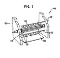
- FIG. 1 illustrates a cut away of a typical PECVD system 100 for large-scale deposition processes - currently up to 2.5 meters wide.
- This system includes a vacuum chamber 105 of which only two walls are illustrated.
- the vacuum chamber houses a linear discharge tube 110.
- the linear discharge tube 110 is formed of an inner conductor 115 that is configured to carry a microwave signal, or other signals, into the vacuum chamber 105.
- This microwave power radiates outward from the inner conductor 115 and ignites the surrounding support gas that is introduced through the support gas tube 120.
- This ignited gas is a plasma and is generally adjacent to the linear discharge tube 110.
- Radicals generated by the plasma and electromagnetic radiation disassociate the feedstock gas(es) 130 introduced through the feedstock gas tube 125 thereby breaking up the feedstock gas to form new molecules.
- Certain molecules formed during the disassociation process are deposited on the substrate 135.
- the other molecules formed by the disassociation process are waste and are removed through an exhaust port (not shown) - although these molecules tend to occasionally deposit themselves on the substrate.
- a substrate carrier moves the substrate 135 through the vacuum chamber 105 at a steady rate.
- Other embodiments could include static coating.
- the disassociation should continue at a steady rate, and target molecules from the disassociated feed gas are theoretically deposited evenly on the substrate, thereby forming a uniform film on the substrate.
- target molecules from the disassociated feed gas are theoretically deposited evenly on the substrate, thereby forming a uniform film on the substrate.
- the films formed by this process are not always uniform. And often, efforts to compensate for these real-world factors damage the substrate by introducing too much heat or other stresses. Accordingly, an improved system and method are needed.
- One embodiment of the present invention is a system for depositing films on a substrate.
- This systems includes a vacuum chamber; a linear discharge tube housed inside the vacuum chamber; a magnetron configured to generate a VHF, microwave, or other high energy power signals that can be applied to the linear discharge tube; a power supply, which can include an electronic amplifier, configured to provide a power signal to the magnetron; and a pulse control connected to the power supply.
- the pulse control is configured to control the duty cycle of the plurality of pulses, the frequency of the plurality of pulses, and/or the contour shape of the plurality of pulse.
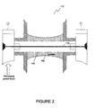
- FIGURE 2 illustrates a non-uniform plasma formed along typical linear discharge tubes 110 used in microwave deposition systems.
- this linear discharge tube 110 is located inside a vacuum chamber (not shown) and includes an inner conductor 115, such as an antenna, inside a non-conductive tube 140.
- Microwave power, or other energy waves is introduced into the inner conductor 115 at both ends of the linear discharge tube 110.
- the microwave power ignites the gas near the linear discharge tube 110 and forms a plasma 142. But as the microwave power travels toward the center of the linear discharge tube 110, the amount of power available to ignite and maintain the plasma drops.
- the plasma 142 near the center of the linear discharge tube 110 may not ignite or may have an extremely low density compared to the plasma 142 at the ends of the linear discharge tube 110. Low power density results in low gas disassociation near the center of the linear discharge tube 110 and low deposition rates near the center of the substrate.
- One system for addressing low plasma density near the center of the linear discharge tube 110 uses a split inner conductor. For example, two conductors are used inside the non-conductive tube. Another system, shown in Figure 3, uses two conductors 145, such as two antennas, and metal shielding 150 placed inside the non-conductive tube 140. The metal shielding 150 and the split antenna 145 act to control the energy discharge and generate a uniform plasma density 142.
- Linear discharge systems are generally driven by a power system, which can include DC supplies and/or amplifiers, coupled to a magnetron. Further enhancements to power-density uniformity and plasma uniformity along the linear discharge tube can be realized by controlling this power system.
- plasma uniformity along the linear discharge tube can be changed by controlling the following properties of a DC signal generated by one type of power system, a DC power system: DC pulse duty cycles, pulse frequencies, and/or signal modulation.
- Signal modulation includes modulation of amplitude or pulse amplitude, frequency, pulse position, pulse width, duty cycle or simultaneous amplitude and any of the frequency types of modulation. Signal modulation is discussed in commonly owned and assigned attorney docket number (APPL-007/00US corresponding to US Serial No.
- microwave power signal being introduced into the inner conductor of the linear discharge tube.
- Changes to the microwave power signal change the plasma uniformity around the linear discharge tube.
- changes to the DC power system can be used to control the plasma properties to thereby increase the uniformity of a chemical make up of the film.
- contouring the power density in the linear discharge tube can be contoured by contouring the power signal being introduced into the inner conductor.
- One method of contouring the power signal being introduced into the inner conductor involves contouring the output of the DC power system.
- the individual pulses of the DC power system can be contoured.
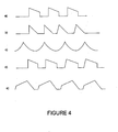
- Figure 4 illustrates five exemplary contoured pulses that can be used to contour the power density in a linear discharge tube.
- the duty cycle, frequency, amplitude, etc. of this signal can also be adjusted.
- the signal can also be modulated.
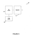
- FIG. 5 illustrates a system constructed in accordance with one embodiment of the present invention.
- This system includes a DC source 160 that is controllable by the pulse control 165.
- the DC source powers the magnetron 170, which generates the microwaves (or other waves) that drive the inner conductor within the linear discharge tube.
- the pulse control 165 can contour the shape of the DC pulses and adjust pulse properties such as duty cycle, frequency, and amplitude.
- FIG 6 it illustrates another embodiment of a system 170 constructed in accordance with the principles of the present invention.
- This system includes the DC source 160 with pulse control 165 and the magnetron 170 also shown in Figure 5.
- This system additionally includes a multiplexer 180 and a timing control system 185.
- the multiplexer 180 is responsible for dividing the output of the magnetron into several signals. Each signal can then be used to power a separate linear discharge tube or separate antenna within a single linear discharge tube.
- the timing control 185 can also be used with linear discharge systems that include multiple magnetrons 170 and/or DC sources 160. In these systems, each linear discharge tube is driven by a separate magnetron and possibly a separate DC source. The timing control can be applied to each magnetron and/or each DC source.
- DC source and “DC power supply” refer to any type of power system, including those that use a linear amplifier, a non-linear amplifier, or no amplifier. The terms can also refer to an amplifier by itself.
- the present invention provides, among other things, a system and method for controlling deposition onto substrates.
- Those skilled in the art can readily recognize that numerous variations and substitutions may be made in the invention, its use and its configuration to achieve substantially the same results as achieved by the embodiments described herein. Accordingly, there is no intention to limit the invention to the disclosed exemplary forms. Many variations, modifications and alternative constructions fall within the scope and spirit of the disclosed invention as expressed in the claims.
Landscapes
- Chemical & Material Sciences (AREA)
- Engineering & Computer Science (AREA)
- General Chemical & Material Sciences (AREA)
- Chemical Kinetics & Catalysis (AREA)
- Materials Engineering (AREA)
- Mechanical Engineering (AREA)
- Metallurgy (AREA)
- Organic Chemistry (AREA)
- Physics & Mathematics (AREA)
- Plasma & Fusion (AREA)
- Chemical Vapour Deposition (AREA)
- Plasma Technology (AREA)
Abstract
Description
- The present invention relates to power supplies, systems, and methods for chemical vapor deposition.
- Chemical vapor deposition (CVD) is a process whereby a film is deposited on a substrate by reacting chemicals together in the gaseous or vapor phase to form a film. The gases or vapors utilized for CVD are gases or compounds that contain the element to be deposited and that may be induced to react with a substrate or other gas(es) to deposit a film. The CVD reaction may be thermally activated, plasma induced, plasma enhanced or activated by light in photon induced systems.
- CVD is used extensively in the semiconductor industry to build up wafers. CVD can also be used for coating larger substrates such as glass and polycarbonate sheets. Plasma enhanced CVD (PECVD), for example, is one of the more promising technologies for creating large photovoltaic sheets and polycarbonate windows for automobiles.
- Figure 1 illustrates a cut away of a
typical PECVD system 100 for large-scale deposition processes - currently up to 2.5 meters wide. This system includes avacuum chamber 105 of which only two walls are illustrated. The vacuum chamber houses alinear discharge tube 110. Thelinear discharge tube 110 is formed of aninner conductor 115 that is configured to carry a microwave signal, or other signals, into thevacuum chamber 105. This microwave power radiates outward from theinner conductor 115 and ignites the surrounding support gas that is introduced through thesupport gas tube 120. This ignited gas is a plasma and is generally adjacent to thelinear discharge tube 110. Radicals generated by the plasma and electromagnetic radiation disassociate the feedstock gas(es) 130 introduced through thefeedstock gas tube 125 thereby breaking up the feedstock gas to form new molecules. Certain molecules formed during the disassociation process are deposited on thesubstrate 135. The other molecules formed by the disassociation process are waste and are removed through an exhaust port (not shown) - although these molecules tend to occasionally deposit themselves on the substrate. - To coat large substrate surface areas rapidly, a substrate carrier moves the
substrate 135 through thevacuum chamber 105 at a steady rate. Other embodiments however, could include static coating. As thesubstrate 135 moves through thevacuum chamber 105, the disassociation should continue at a steady rate, and target molecules from the disassociated feed gas are theoretically deposited evenly on the substrate, thereby forming a uniform film on the substrate. But due to a variety of real-world factors, the films formed by this process are not always uniform. And often, efforts to compensate for these real-world factors damage the substrate by introducing too much heat or other stresses. Accordingly, an improved system and method are needed. - Exemplary embodiments of the present invention that are shown in the drawings are summarized below. These and other embodiments are more fully described in the Detailed Description section. It is to be understood, however, that there is no intention to limit the invention to the forms described in this Summary of the Invention or in the Detailed Description. One skilled in the art can recognize that there are numerous modifications, equivalents and alternative constructions that fall within the spirit and scope of the invention as expressed in the claims.
- One embodiment of the present invention is a system for depositing films on a substrate. This systems includes a vacuum chamber; a linear discharge tube housed inside the vacuum chamber; a magnetron configured to generate a VHF, microwave, or other high energy power signals that can be applied to the linear discharge tube; a power supply, which can include an electronic amplifier, configured to provide a power signal to the magnetron; and a pulse control connected to the power supply. The pulse control is configured to control the duty cycle of the plurality of pulses, the frequency of the plurality of pulses, and/or the contour shape of the plurality of pulse.
- Various objects and advantages and a more complete understanding of the present invention are apparent and more readily appreciated by reference to the following Detailed Description and to the appended claims when taken in conjunction with the accompanying Drawing wherein:
- FIGURE 1 is an illustration of an existing linear PECVD system;
- FIGURE 2 is an illustration of a linear discharge tube with surrounding, irregular plasma;
- FIGURE 3 is an illustration of a shielded split antennae arrangement for a linear discharge tube;
- FIGURE 4 illustrates exemplary power source signals that can be used with the present invention;
- FIGURE 5 is an illustration of a power source in accordance with one embodiment of the present invention; and
- FIGURE 6 is an illustration of another power source in accordance with an embodiment of the present invention.
- As previously described, real-world factors act to limit the quality of films created by deposition systems, including linear microwave deposition systems. One of these limiting factors is an inability to create and maintain uniform plasmas around the linear discharge tube. Non-uniform plasmas result in non-uniform disassociation at certain points along the linear discharge tube, thereby causing non-homogenous deposition on certain portions of the substrate.
- FIGURE 2 illustrates a non-uniform plasma formed along typical
linear discharge tubes 110 used in microwave deposition systems. For perspective, thislinear discharge tube 110 is located inside a vacuum chamber (not shown) and includes aninner conductor 115, such as an antenna, inside anon-conductive tube 140. Microwave power, or other energy waves, is introduced into theinner conductor 115 at both ends of thelinear discharge tube 110. The microwave power ignites the gas near thelinear discharge tube 110 and forms aplasma 142. But as the microwave power travels toward the center of thelinear discharge tube 110, the amount of power available to ignite and maintain the plasma drops. In certain cases, theplasma 142 near the center of thelinear discharge tube 110 may not ignite or may have an extremely low density compared to theplasma 142 at the ends of thelinear discharge tube 110. Low power density results in low gas disassociation near the center of thelinear discharge tube 110 and low deposition rates near the center of the substrate. - One system for addressing low plasma density near the center of the
linear discharge tube 110 uses a split inner conductor. For example, two conductors are used inside the non-conductive tube. Another system, shown in Figure 3, uses twoconductors 145, such as two antennas, andmetal shielding 150 placed inside thenon-conductive tube 140. Themetal shielding 150 and thesplit antenna 145 act to control the energy discharge and generate auniform plasma density 142. - Linear discharge systems are generally driven by a power system, which can include DC supplies and/or amplifiers, coupled to a magnetron. Further enhancements to power-density uniformity and plasma uniformity along the linear discharge tube can be realized by controlling this power system. For example, plasma uniformity along the linear discharge tube can be changed by controlling the following properties of a DC signal generated by one type of power system, a DC power system: DC pulse duty cycles, pulse frequencies, and/or signal modulation. Signal modulation includes modulation of amplitude or pulse amplitude, frequency, pulse position, pulse width, duty cycle or simultaneous amplitude and any of the frequency types of modulation. Signal modulation is discussed in commonly owned and assigned attorney docket number (APPL-007/00US corresponding to
US Serial No. 11/264,596 - Each of these changes directly changes the microwave power signal being introduced into the inner conductor of the linear discharge tube. Changes to the microwave power signal change the plasma uniformity around the linear discharge tube. And in many cases, changes to the DC power system can be used to control the plasma properties to thereby increase the uniformity of a chemical make up of the film. These enhancements to the power supply can be applied to single antenna systems, multiple antenna systems, multiple antenna systems with shields, etc.
- Even further enhancements to a deposition system can be realized by contouring the power density in the linear discharge tube. The power density can be contoured by contouring the power signal being introduced into the inner conductor. One method of contouring the power signal being introduced into the inner conductor involves contouring the output of the DC power system. For example, the individual pulses of the DC power system can be contoured. Figure 4 illustrates five exemplary contoured pulses that can be used to contour the power density in a linear discharge tube. The duty cycle, frequency, amplitude, etc. of this signal can also be adjusted. The signal can also be modulated.
- Particularly good results are anticipated when the degrading-pulse contours shown in Figures 4a, 4b, 4c and 4d are used. This degrading pulse helps maintain a uniform power density along the entire length of the linear discharge tube as the plasma ignition travels from the outer edges toward the center of the linear discharge tube. These enhancements can be applied to single antenna systems, dual antenna systems, dual antenna systems with shields, etc. These enhancements can also be used to evenly coat curved substrates as well as flat substrates because of the control of local densities.
- Figure 5 illustrates a system constructed in accordance with one embodiment of the present invention. This system includes a
DC source 160 that is controllable by thepulse control 165. The DC source powers themagnetron 170, which generates the microwaves (or other waves) that drive the inner conductor within the linear discharge tube. Thepulse control 165 can contour the shape of the DC pulses and adjust pulse properties such as duty cycle, frequency, and amplitude. - Referring now to Figure 6, it illustrates another embodiment of a
system 170 constructed in accordance with the principles of the present invention. This system includes theDC source 160 withpulse control 165 and themagnetron 170 also shown in Figure 5. This system additionally includes amultiplexer 180 and atiming control system 185. Themultiplexer 180 is responsible for dividing the output of the magnetron into several signals. Each signal can then be used to power a separate linear discharge tube or separate antenna within a single linear discharge tube. - Recall that most linear discharge deposition systems include several linear discharge tubes. In certain instances, it may be desirable to offset the timing of the pulses driving adjacent linear discharge tubes. The microwaves generated by one linear discharge tube can travel to adjacent linear discharge tubes and impact power density and plasma uniformity. With proper timing control, that impact can be positive and can assist with maintaining a uniform power density and plasma. The
timing control 185 can provide this timing control. These of skill in the art would understand how to tune the timing control. - The
timing control 185 can also be used with linear discharge systems that includemultiple magnetrons 170 and/orDC sources 160. In these systems, each linear discharge tube is driven by a separate magnetron and possibly a separate DC source. The timing control can be applied to each magnetron and/or each DC source. The terms "DC source" and "DC power supply" refer to any type of power system, including those that use a linear amplifier, a non-linear amplifier, or no amplifier. The terms can also refer to an amplifier by itself. - In conclusion, the present invention provides, among other things, a system and method for controlling deposition onto substrates. Those skilled in the art can readily recognize that numerous variations and substitutions may be made in the invention, its use and its configuration to achieve substantially the same results as achieved by the embodiments described herein. Accordingly, there is no intention to limit the invention to the disclosed exemplary forms. Many variations, modifications and alternative constructions fall within the scope and spirit of the disclosed invention as expressed in the claims.
Claims (14)
- A system for depositing films on a substrate, the system comprising:a vacuum chamber;a linear discharge tube housed inside the vacuum chamber;a magnetron configured to generate a microwave power signal that can be applied to the linear discharge tube;a power supply configured to provide a power signal to the magnetron, the DC power signal including a plurality of pulses; anda pulse control connected to the power supply, the pulse control configured to control the duty cycle of the plurality of pulses, the frequency of the plurality of pulses, and the contour shape of the plurality of pulses.
- The system of claim 1, wherein the pulse control is configured to decrease or increase the power of one of the plurality of pulses.
- The system of claim 1, wherein the linear discharge tube is a first linear discharge tube, the system further comprising:a second linear discharge tube; anda multiplexer connected to the first linear discharge tube, the second linear discharge tube, and the magnetron.
- The system of claim 1, wherein the linear discharge tube comprises:a non-conductive outer layer,two inner conductors located inside the non-conductive outer layer; anda metal shield located adjacent to the two inner conductors and the non-conductive outer layer.
- A power system for film deposition, the system comprising:a magnetron configured to generate a microwave power signal for driving a linear discharge tube in a film deposition system;a power source connected to the magnetron, the power source configured to generate a plurality of pulses; anda control system connected to the power source, the control system configured to control the contour shape of the plurality of pulses to thereby control the output of the magnetron and the operation of the linear discharge tube in the film deposition system.
- The system of claim 5, wherein the control system is further configured to control the duty cycle of the plurality of pulses to thereby control the output of the magnetron and the operation of the linear discharge tube in the film deposition system.
- The system of claim 5, wherein the control system is further configured to control the frequency of the plurality of pulses to thereby control the output of the magnetron and the operation of the linear discharge tube in the film deposition system.
- A method to deposit films on a substrate, the method comprising:generating a DC pulse with a contoured shape;generating a microwave power signal using the contoured DC pulse;providing the generated microwave power signal to a linear discharge tube located in a film deposition system;generating a plasma at the linear discharge tube using the generated microwave power signal;disassociating a gas using the generated plasma; anddepositing a portion of the disassociated gas onto a substrate.
- A power system for film deposition, the system comprising:a magnetron configured to generate a microwave power signal that can be applied to the linear discharge tube;an amplifier configured to provide a DC signal to the magnetron, the DC signal including a plurality of pulses; anda pulse control connected to the amplifier, the pulse control configured to control the duty cycle of the plurality of pulses, the frequency of the plurality of pulses, and the contour shape of the plurality of pulses.
- The system of claim 9, wherein the amplifier is a linear amplifier.
- The system of claim 9, wherein the amplifier is a non-linear amplifier.
- The system of claim 9, further comprising a multiplexer connected to the output of the magnetron.
- The system of claim 9, wherein the pulse control is configured to contour the shape of one of the plurality of pulses so that the power of the one of the plurality of pulses decreases from an initial power point for the one of the plurality of pulses.
- The system of claim 9, wherein the pulse control is configured to contour the shape of one of the plurality of pulses so that the power of the one of the plurality of pulses increases from an initial power point for the one of the plurality of pulses.
Applications Claiming Priority (1)
| Application Number | Priority Date | Filing Date | Title |
|---|---|---|---|
| US11/264,540 US20070095281A1 (en) | 2005-11-01 | 2005-11-01 | System and method for power function ramping of microwave liner discharge sources |
Publications (2)
| Publication Number | Publication Date |
|---|---|
| EP1780303A2 true EP1780303A2 (en) | 2007-05-02 |
| EP1780303A3 EP1780303A3 (en) | 2010-07-07 |
Family
ID=37753131
Family Applications (1)
| Application Number | Title | Priority Date | Filing Date |
|---|---|---|---|
| EP06022261A Withdrawn EP1780303A3 (en) | 2005-11-01 | 2006-10-25 | System and method for power function ramping of microwave linear discharge sources |
Country Status (6)
| Country | Link |
|---|---|
| US (2) | US20070095281A1 (en) |
| EP (1) | EP1780303A3 (en) |
| JP (1) | JP2007126742A (en) |
| KR (1) | KR100821811B1 (en) |
| CN (1) | CN1958843A (en) |
| TW (1) | TWI324637B (en) |
Cited By (3)
| Publication number | Priority date | Publication date | Assignee | Title |
|---|---|---|---|---|
| EP2618640A2 (en) * | 2012-01-23 | 2013-07-24 | Forschungsverbund Berlin e.V. | Method and apparatus for generating plasma pulses |
| ITRM20130161A1 (en) * | 2013-03-15 | 2014-09-15 | Consiglio Nazionale Ricerche | REINFORCED MICROWAVE POWERED LAMP |
| ITRM20130159A1 (en) * | 2013-03-15 | 2014-09-15 | Consiglio Nazionale Ricerche | ELONGATED MICROWAVE POWERED LAMP |
Families Citing this family (10)
| Publication number | Priority date | Publication date | Assignee | Title |
|---|---|---|---|---|
| TW200845833A (en) * | 2007-05-01 | 2008-11-16 | Delta Electronics Inc | Plasma generating device |
| CN101945689B (en) * | 2008-01-30 | 2012-07-18 | 应用材料公司 | Systems and methods for plasma discharge sources for preionized surface wave emission |
| WO2009096953A1 (en) * | 2008-01-30 | 2009-08-06 | Applied Materials, Inc. | Integrated microwave waveguide with impedance transition |
| TW201105183A (en) * | 2009-07-21 | 2011-02-01 | Delta Electronics Inc | Plasma generating apparatus |
| DE102009044496B4 (en) * | 2009-11-11 | 2023-11-02 | Muegge Gmbh | Device for generating plasma using microwaves |
| WO2011137371A2 (en) * | 2010-04-30 | 2011-11-03 | Applied Materials, Inc. | Vertical inline cvd system |
| JP5820661B2 (en) * | 2010-09-14 | 2015-11-24 | 東京エレクトロン株式会社 | Microwave irradiation device |
| KR102168063B1 (en) * | 2012-01-27 | 2020-10-20 | 어플라이드 머티어리얼스, 인코포레이티드 | Segmented antenna assembly |
| CN111933502B (en) * | 2020-08-10 | 2023-05-05 | 电子科技大学 | Power source system based on pulse magnetron duty cycle synthesis |
| JP7751179B2 (en) * | 2021-08-03 | 2025-10-08 | 日新電機株式会社 | Plasma processing equipment |
Family Cites Families (99)
| Publication number | Priority date | Publication date | Assignee | Title |
|---|---|---|---|---|
| US521638A (en) * | 1894-06-19 | oleal | ||
| EP0045822B1 (en) * | 1980-08-08 | 1985-05-29 | Battelle Development Corporation | Cylindrical magnetron sputtering cathode |
| US4356073A (en) * | 1981-02-12 | 1982-10-26 | Shatterproof Glass Corporation | Magnetron cathode sputtering apparatus |
| US4422916A (en) * | 1981-02-12 | 1983-12-27 | Shatterproof Glass Corporation | Magnetron cathode sputtering apparatus |
| US4417968A (en) * | 1983-03-21 | 1983-11-29 | Shatterproof Glass Corporation | Magnetron cathode sputtering apparatus |
| US4443318A (en) * | 1983-08-17 | 1984-04-17 | Shatterproof Glass Corporation | Cathodic sputtering apparatus |
| US4445997A (en) * | 1983-08-17 | 1984-05-01 | Shatterproof Glass Corporation | Rotatable sputtering apparatus |
| US4466877A (en) * | 1983-10-11 | 1984-08-21 | Shatterproof Glass Corporation | Magnetron cathode sputtering apparatus |
| US4519885A (en) * | 1983-12-27 | 1985-05-28 | Shatterproof Glass Corp. | Method and apparatus for changing sputtering targets in a magnetron sputtering system |
| US4566403A (en) * | 1985-01-30 | 1986-01-28 | Sovonics Solar Systems | Apparatus for microwave glow discharge deposition |
| US4904362A (en) * | 1987-07-24 | 1990-02-27 | Miba Gleitlager Aktiengesellschaft | Bar-shaped magnetron or sputter cathode arrangement |
| JP2792558B2 (en) * | 1987-12-07 | 1998-09-03 | 株式会社日立製作所 | Surface treatment device and surface treatment method |
| US5354446A (en) * | 1988-03-03 | 1994-10-11 | Asahi Glass Company Ltd. | Ceramic rotatable magnetron sputtering cathode target and process for its production |
| DE3821207A1 (en) * | 1988-06-23 | 1989-12-28 | Leybold Ag | ARRANGEMENT FOR COATING A SUBSTRATE WITH DIELECTRICS |
| US4837185A (en) * | 1988-10-26 | 1989-06-06 | Intel Corporation | Pulsed dual radio frequency CVD process |
| US4927515A (en) * | 1989-01-09 | 1990-05-22 | The Board Of Trustees Of The Leland Stanford Junior University | Circular magnetron sputtering device |
| US5047131A (en) * | 1989-11-08 | 1991-09-10 | The Boc Group, Inc. | Method for coating substrates with silicon based compounds |
| US5096562A (en) * | 1989-11-08 | 1992-03-17 | The Boc Group, Inc. | Rotating cylindrical magnetron structure for large area coating |
| BE1003701A3 (en) * | 1990-06-08 | 1992-05-26 | Saint Roch Glaceries | Rotary cathode. |
| WO1992002659A1 (en) * | 1990-08-10 | 1992-02-20 | Viratec Thin Films, Inc. | Shielding for arc suppression in rotating magnetron sputtering systems |
| US5200049A (en) * | 1990-08-10 | 1993-04-06 | Viratec Thin Films, Inc. | Cantilever mount for rotating cylindrical magnetrons |
| JP2687966B2 (en) * | 1990-08-20 | 1997-12-08 | 富士通株式会社 | Method for manufacturing semiconductor device |
| US5156727A (en) * | 1990-10-12 | 1992-10-20 | Viratec Thin Films, Inc. | Film thickness uniformity control apparatus for in-line sputtering systems |
| US5100527A (en) * | 1990-10-18 | 1992-03-31 | Viratec Thin Films, Inc. | Rotating magnetron incorporating a removable cathode |
| US5106474A (en) * | 1990-11-21 | 1992-04-21 | Viratec Thin Films, Inc. | Anode structures for magnetron sputtering apparatus |
| US5108574A (en) * | 1991-01-29 | 1992-04-28 | The Boc Group, Inc. | Cylindrical magnetron shield structure |
| DE4106770C2 (en) * | 1991-03-04 | 1996-10-17 | Leybold Ag | Performing reactive coating of a substrate |
| US5171411A (en) * | 1991-05-21 | 1992-12-15 | The Boc Group, Inc. | Rotating cylindrical magnetron structure with self supporting zinc alloy target |
| US5262032A (en) * | 1991-05-28 | 1993-11-16 | Leybold Aktiengesellschaft | Sputtering apparatus with rotating target and target cooling |
| US5364518A (en) * | 1991-05-28 | 1994-11-15 | Leybold Aktiengesellschaft | Magnetron cathode for a rotating target |
| DE4117518C2 (en) * | 1991-05-29 | 2000-06-21 | Leybold Ag | Device for sputtering with a moving, in particular rotating, target |
| DE4126236C2 (en) * | 1991-08-08 | 2000-01-05 | Leybold Ag | Rotating magnetron cathode and use of a rotating magnetron cathode |
| JPH08977B2 (en) * | 1991-08-22 | 1996-01-10 | 日新電機株式会社 | Plasma CVD method and apparatus |
| GB9121665D0 (en) * | 1991-10-11 | 1991-11-27 | Boc Group Plc | Sputtering processes and apparatus |
| DE4136297A1 (en) * | 1991-11-04 | 1993-05-06 | Plasma Electronic Gmbh, 7024 Filderstadt, De | Localised plasma prodn. in treatment chamber - using microwave generator connected to coupling device which passes through the wall of the chamber without using a coupling window |
| IT1262897B (en) * | 1992-03-11 | 1996-07-22 | Proel Tecnologie Spa | PERFECTED PLASMA GENERATOR AND RELATED IONIZATION METHOD |
| JPH0697087A (en) * | 1992-09-17 | 1994-04-08 | Hitachi Ltd | Plasma treatment apparatus |
| US5338422A (en) * | 1992-09-29 | 1994-08-16 | The Boc Group, Inc. | Device and method for depositing metal oxide films |
| JPH08506855A (en) * | 1993-01-15 | 1996-07-23 | ザ ビーオーシー グループ インコーポレイテッド | Cylindrical magnetron shield structure |
| US5385578A (en) * | 1993-02-18 | 1995-01-31 | Ventritex, Inc. | Electrical connection for medical electrical stimulation electrodes |
| US5344792A (en) * | 1993-03-04 | 1994-09-06 | Micron Technology, Inc. | Pulsed plasma enhanced CVD of metal silicide conductive films such as TiSi2 |
| US5540781A (en) * | 1993-03-23 | 1996-07-30 | Canon Kabushiki Kaisha | Plasma CVD process using a very-high-frequency and plasma CVD apparatus |
| CA2120875C (en) * | 1993-04-28 | 1999-07-06 | The Boc Group, Inc. | Durable low-emissivity solar control thin film coating |
| CA2123479C (en) * | 1993-07-01 | 1999-07-06 | Peter A. Sieck | Anode structure for magnetron sputtering systems |
| US5648293A (en) * | 1993-07-22 | 1997-07-15 | Nec Corporation | Method of growing an amorphous silicon film |
| JP3026704B2 (en) * | 1993-07-29 | 2000-03-27 | 富士通株式会社 | Magnetron oscillation output control device and plasma processing method |
| DE69408405T2 (en) * | 1993-11-11 | 1998-08-20 | Nissin Electric Co Ltd | Plasma CVD method and device |
| US5620577A (en) * | 1993-12-30 | 1997-04-15 | Viratec Thin Films, Inc. | Spring-loaded mount for a rotatable sputtering cathode |
| US5567289A (en) * | 1993-12-30 | 1996-10-22 | Viratec Thin Films, Inc. | Rotating floating magnetron dark-space shield and cone end |
| US5616225A (en) * | 1994-03-23 | 1997-04-01 | The Boc Group, Inc. | Use of multiple anodes in a magnetron for improving the uniformity of its plasma |
| DE4418906B4 (en) * | 1994-05-31 | 2004-03-25 | Unaxis Deutschland Holding Gmbh | Process for coating a substrate and coating system for carrying it out |
| JP2829241B2 (en) * | 1994-07-26 | 1998-11-25 | 三菱電機株式会社 | Plant support equipment |
| US5571393A (en) * | 1994-08-24 | 1996-11-05 | Viratec Thin Films, Inc. | Magnet housing for a sputtering cathode |
| US5445721A (en) * | 1994-08-25 | 1995-08-29 | The Boc Group, Inc. | Rotatable magnetron including a replacement target structure |
| US5518592A (en) * | 1994-08-25 | 1996-05-21 | The Boc Group, Inc. | Seal cartridge for a rotatable magnetron |
| ZA956811B (en) * | 1994-09-06 | 1996-05-14 | Boc Group Inc | Dual cylindrical target magnetron with multiple anodes |
| DE4445427C2 (en) * | 1994-12-20 | 1997-04-30 | Schott Glaswerke | Plasma CVD method for producing a gradient layer |
| US5527439A (en) * | 1995-01-23 | 1996-06-18 | The Boc Group, Inc. | Cylindrical magnetron shield structure |
| WO1996034124A1 (en) * | 1995-04-25 | 1996-10-31 | The Boc Group, Inc. | Sputtering system using cylindrical rotating magnetron electrically powered using alternating current |
| DE19623359A1 (en) * | 1995-08-17 | 1997-02-20 | Leybold Ag | Device for coating a substrate by vaporisation of a rotary tubular target |
| DE69628441T2 (en) * | 1995-10-13 | 2004-04-29 | Dow Global Technologies, Inc., Midland | METHOD FOR PRODUCING COATED PLASTIC SURFACES |
| US5591314A (en) * | 1995-10-27 | 1997-01-07 | Morgan; Steven V. | Apparatus for affixing a rotating cylindrical magnetron target to a spindle |
| DE19634795C2 (en) * | 1996-08-29 | 1999-11-04 | Schott Glas | Plasma CVD system with an array of microwave plasma electrodes and plasma CVD processes |
| JPH10104862A (en) | 1996-09-30 | 1998-04-24 | Kyocera Corp | Manufacturing method of electrophotographic photoreceptor |
| DE19651378A1 (en) * | 1996-12-11 | 1998-06-18 | Leybold Systems Gmbh | Insulating thin film sputter deposition apparatus |
| DE19722272A1 (en) * | 1997-05-28 | 1998-12-03 | Leybold Systems Gmbh | Device for generating plasma |
| JP4120974B2 (en) * | 1997-06-17 | 2008-07-16 | キヤノンアネルバ株式会社 | Thin film manufacturing method and thin film manufacturing apparatus |
| JP3559429B2 (en) | 1997-07-02 | 2004-09-02 | 松下電器産業株式会社 | Plasma processing method |
| JPH1129863A (en) * | 1997-07-10 | 1999-02-02 | Canon Inc | Deposition film manufacturing method |
| JPH11214196A (en) * | 1998-01-29 | 1999-08-06 | Mitsubishi Electric Corp | Plasma generator |
| US6203862B1 (en) * | 1998-05-13 | 2001-03-20 | Intevac, Inc. | Processing systems with dual ion sources |
| DE19824077A1 (en) * | 1998-05-29 | 1999-12-02 | Leybold Systems Gmbh | Device for generating plasma |
| DE19825125A1 (en) * | 1998-06-05 | 1999-12-09 | Leybold Systems Gmbh | Device for generating plasma |
| WO2000003566A1 (en) * | 1998-07-13 | 2000-01-20 | Toshiyuki Takamatsu | Microwave discharge apparatus |
| US6126778A (en) * | 1998-07-22 | 2000-10-03 | Micron Technology, Inc. | Beat frequency modulation for plasma generation |
| US5985375A (en) * | 1998-09-03 | 1999-11-16 | Micron Technology, Inc. | Method for pulsed-plasma enhanced vapor deposition |
| WO2000028104A1 (en) * | 1998-11-06 | 2000-05-18 | Scivac | Sputtering apparatus and process for high rate coatings |
| FR2798552B1 (en) * | 1999-09-13 | 2001-11-30 | Centre Nat Rech Scient | DEVICE FOR PROVIDING A PREDETERMINED MICROWAVE POWER DIVISION ON A PLURALITY OF LOADS, PARTICULARLY FOR THE PRODUCTION OF PLASMA |
| DE19953470A1 (en) * | 1999-11-05 | 2001-05-23 | Heraeus Gmbh W C | Tube target |
| DE60134081D1 (en) * | 2000-04-13 | 2008-07-03 | Ihi Corp | Production method of thin films, device for the production of thin films and solar cell |
| US6582572B2 (en) * | 2000-06-01 | 2003-06-24 | Seagate Technology Llc | Target fabrication method for cylindrical cathodes |
| JP4516199B2 (en) * | 2000-09-13 | 2010-08-04 | キヤノンアネルバ株式会社 | Sputtering apparatus and electronic device manufacturing method |
| JP4557400B2 (en) * | 2000-09-14 | 2010-10-06 | キヤノン株式会社 | Method for forming deposited film |
| US20020189939A1 (en) * | 2001-06-14 | 2002-12-19 | German John R. | Alternating current rotatable sputter cathode |
| WO2002084702A2 (en) * | 2001-01-16 | 2002-10-24 | Lampkin Curtis M | Sputtering deposition apparatus and method for depositing surface films |
| US6726804B2 (en) * | 2001-01-22 | 2004-04-27 | Liang-Guo Wang | RF power delivery for plasma processing using modulated power signal |
| US6375815B1 (en) * | 2001-02-17 | 2002-04-23 | David Mark Lynn | Cylindrical magnetron target and apparatus for affixing the target to a rotatable spindle assembly |
| JP3833489B2 (en) * | 2001-03-29 | 2006-10-11 | 株式会社東芝 | Cold cathode discharge device |
| US6635154B2 (en) * | 2001-11-03 | 2003-10-21 | Intevac, Inc. | Method and apparatus for multi-target sputtering |
| DE10154229B4 (en) * | 2001-11-07 | 2004-08-05 | Applied Films Gmbh & Co. Kg | Device for the regulation of a plasma impedance |
| US6736948B2 (en) * | 2002-01-18 | 2004-05-18 | Von Ardenne Anlagentechnik Gmbh | Cylindrical AC/DC magnetron with compliant drive system and improved electrical and thermal isolation |
| JP2004055614A (en) * | 2002-07-16 | 2004-02-19 | Tokyo Electron Ltd | Plasma processing equipment |
| US7445690B2 (en) * | 2002-10-07 | 2008-11-04 | Tokyo Electron Limited | Plasma processing apparatus |
| KR20050084844A (en) * | 2002-10-09 | 2005-08-29 | 도요 세이칸 가부시키가이샤 | Method of forming metal oxide film and microwave power source unit for use in the method |
| TW200420201A (en) * | 2002-12-16 | 2004-10-01 | Japan Science & Tech Agency | Plasma generation device, plasma control method and substrate manufacturing method |
| US20040112735A1 (en) * | 2002-12-17 | 2004-06-17 | Applied Materials, Inc. | Pulsed magnetron for sputter deposition |
| WO2004062326A2 (en) * | 2002-12-30 | 2004-07-22 | Northeastern University | Low power plasma generator |
| US6923891B2 (en) * | 2003-01-10 | 2005-08-02 | Nanofilm Technologies International Pte Ltd. | Copper interconnects |
| JP4204505B2 (en) * | 2004-03-31 | 2009-01-07 | 日本高周波株式会社 | Magnetron oscillator |
-
2005
- 2005-11-01 US US11/264,540 patent/US20070095281A1/en not_active Abandoned
-
2006
- 2006-06-01 TW TW095119435A patent/TWI324637B/en active
- 2006-06-14 JP JP2006165169A patent/JP2007126742A/en active Pending
- 2006-06-27 CN CNA200610094141XA patent/CN1958843A/en active Pending
- 2006-07-04 KR KR1020060062234A patent/KR100821811B1/en not_active Expired - Fee Related
- 2006-10-25 EP EP06022261A patent/EP1780303A3/en not_active Withdrawn
-
2007
- 2007-02-23 US US11/678,448 patent/US20080286495A1/en not_active Abandoned
Cited By (5)
| Publication number | Priority date | Publication date | Assignee | Title |
|---|---|---|---|---|
| EP2618640A2 (en) * | 2012-01-23 | 2013-07-24 | Forschungsverbund Berlin e.V. | Method and apparatus for generating plasma pulses |
| ITRM20130161A1 (en) * | 2013-03-15 | 2014-09-15 | Consiglio Nazionale Ricerche | REINFORCED MICROWAVE POWERED LAMP |
| ITRM20130159A1 (en) * | 2013-03-15 | 2014-09-15 | Consiglio Nazionale Ricerche | ELONGATED MICROWAVE POWERED LAMP |
| WO2014141183A1 (en) | 2013-03-15 | 2014-09-18 | Consiglio Nazionale Delle Ricerche | Elongated microwave powered lamp |
| WO2014141185A1 (en) * | 2013-03-15 | 2014-09-18 | Consiglio Nazionale Delle Ricerche | Reinforced microwave powered lamp |
Also Published As
| Publication number | Publication date |
|---|---|
| TW200718799A (en) | 2007-05-16 |
| KR100821811B1 (en) | 2008-04-11 |
| CN1958843A (en) | 2007-05-09 |
| EP1780303A3 (en) | 2010-07-07 |
| KR20070047203A (en) | 2007-05-04 |
| US20080286495A1 (en) | 2008-11-20 |
| JP2007126742A (en) | 2007-05-24 |
| US20070095281A1 (en) | 2007-05-03 |
| TWI324637B (en) | 2010-05-11 |
Similar Documents
| Publication | Publication Date | Title |
|---|---|---|
| US20080286495A1 (en) | System and method for power function ramping of split antenna pecvd discharge sources | |
| US20100078320A1 (en) | Microwave plasma containment shield shaping | |
| US5985378A (en) | Remote-plasma-CVD method for coating or for treating large-surface substrates and apparatus for performing same | |
| US10734198B2 (en) | Microwave plasma reactor for manufacturing synthetic diamond material | |
| US5626922A (en) | Plasma processing method | |
| US20110076422A1 (en) | Curved microwave plasma line source for coating of three-dimensional substrates | |
| US7842355B2 (en) | System and method for modulation of power and power related functions of PECVD discharge sources to achieve new film properties | |
| WO2008052706A1 (en) | Method of forming a film by deposition from a plasma | |
| CN101945689B (en) | Systems and methods for plasma discharge sources for preionized surface wave emission | |
| US8536955B2 (en) | Integrated microwave waveguide block with tapered impedance transition sections | |
| Liehr et al. | Large area microwave coating technology | |
| US6916512B2 (en) | Method and device for coating substrates | |
| KR101781290B1 (en) | Large scale Surface Wave Plasma Device and Conductive Diamond Coating using the Device | |
| KR100824171B1 (en) | Method and system for modulation of power and power related functions of a PCCD discharge source to obtain new thin film properties | |
| KR20060082400A (en) | Plasma generating system | |
| EP1921659A2 (en) | System and method for control of electromagnetic radiation in PECVD discharge processes | |
| WO2009096954A1 (en) | System and method for microwave plasma species source | |
| KR20040088650A (en) | A apparatus for synthesis of thin films | |
| JP2001295052A (en) | Thin film forming method, thin film forming apparatus, and solar cell |
Legal Events
| Date | Code | Title | Description |
|---|---|---|---|
| PUAI | Public reference made under article 153(3) epc to a published international application that has entered the european phase |
Free format text: ORIGINAL CODE: 0009012 |
|
| AK | Designated contracting states |
Kind code of ref document: A2 Designated state(s): AT BE BG CH CY CZ DE DK EE ES FI FR GB GR HU IE IS IT LI LT LU LV MC NL PL PT RO SE SI SK TR |
|
| AX | Request for extension of the european patent |
Extension state: AL BA HR MK YU |
|
| RAP1 | Party data changed (applicant data changed or rights of an application transferred) |
Owner name: APPLIED MATERIALS GMBH & CO. KG Owner name: APPLIED MATERIALS, INC. |
|
| PUAL | Search report despatched |
Free format text: ORIGINAL CODE: 0009013 |
|
| AK | Designated contracting states |
Kind code of ref document: A3 Designated state(s): AT BE BG CH CY CZ DE DK EE ES FI FR GB GR HU IE IS IT LI LT LU LV MC NL PL PT RO SE SI SK TR |
|
| AX | Request for extension of the european patent |
Extension state: AL BA HR MK RS |
|
| AKY | No designation fees paid | ||
| STAA | Information on the status of an ep patent application or granted ep patent |
Free format text: STATUS: THE APPLICATION IS DEEMED TO BE WITHDRAWN |
|
| 18D | Application deemed to be withdrawn |
Effective date: 20110111 |