EP1780175A2 - Method for assembling MEMS parts - Google Patents
Method for assembling MEMS parts Download PDFInfo
- Publication number
- EP1780175A2 EP1780175A2 EP06122979A EP06122979A EP1780175A2 EP 1780175 A2 EP1780175 A2 EP 1780175A2 EP 06122979 A EP06122979 A EP 06122979A EP 06122979 A EP06122979 A EP 06122979A EP 1780175 A2 EP1780175 A2 EP 1780175A2
- Authority
- EP
- European Patent Office
- Prior art keywords
- silicon wafer
- segment
- wafer segment
- inertial sensor
- applying
- Prior art date
- Legal status (The legal status is an assumption and is not a legal conclusion. Google has not performed a legal analysis and makes no representation as to the accuracy of the status listed.)
- Withdrawn
Links
Images




Classifications
-
- B—PERFORMING OPERATIONS; TRANSPORTING
- B81—MICROSTRUCTURAL TECHNOLOGY
- B81C—PROCESSES OR APPARATUS SPECIALLY ADAPTED FOR THE MANUFACTURE OR TREATMENT OF MICROSTRUCTURAL DEVICES OR SYSTEMS
- B81C3/00—Assembling of devices or systems from individually processed components
- B81C3/002—Aligning microparts
-
- H—ELECTRICITY
- H10—SEMICONDUCTOR DEVICES; ELECTRIC SOLID-STATE DEVICES NOT OTHERWISE PROVIDED FOR
- H10D—INORGANIC ELECTRIC SEMICONDUCTOR DEVICES
- H10D99/00—Subject matter not provided for in other groups of this subclass
-
- B—PERFORMING OPERATIONS; TRANSPORTING
- B81—MICROSTRUCTURAL TECHNOLOGY
- B81B—MICROSTRUCTURAL DEVICES OR SYSTEMS, e.g. MICROMECHANICAL DEVICES
- B81B7/00—Microstructural systems ; Auxiliary parts of microstructural devices or systems
- B81B7/0032—Packages or encapsulation
- B81B7/0074—3D packaging, i.e. encapsulation containing one or several MEMS devices arranged in planes non-parallel to the mounting board
-
- G—PHYSICS
- G01—MEASURING; TESTING
- G01P—MEASURING LINEAR OR ANGULAR SPEED, ACCELERATION, DECELERATION, OR SHOCK; INDICATING PRESENCE, ABSENCE, OR DIRECTION, OF MOVEMENT
- G01P1/00—Details of instruments
- G01P1/02—Housings
- G01P1/023—Housings for acceleration measuring devices
-
- G—PHYSICS
- G01—MEASURING; TESTING
- G01P—MEASURING LINEAR OR ANGULAR SPEED, ACCELERATION, DECELERATION, OR SHOCK; INDICATING PRESENCE, ABSENCE, OR DIRECTION, OF MOVEMENT
- G01P15/00—Measuring acceleration; Measuring deceleration; Measuring shock, i.e. sudden change of acceleration
- G01P15/02—Measuring acceleration; Measuring deceleration; Measuring shock, i.e. sudden change of acceleration by making use of inertia forces using solid seismic masses
- G01P15/08—Measuring acceleration; Measuring deceleration; Measuring shock, i.e. sudden change of acceleration by making use of inertia forces using solid seismic masses with conversion into electric or magnetic values
- G01P15/0802—Details
-
- G—PHYSICS
- G01—MEASURING; TESTING
- G01P—MEASURING LINEAR OR ANGULAR SPEED, ACCELERATION, DECELERATION, OR SHOCK; INDICATING PRESENCE, ABSENCE, OR DIRECTION, OF MOVEMENT
- G01P15/00—Measuring acceleration; Measuring deceleration; Measuring shock, i.e. sudden change of acceleration
- G01P15/18—Measuring acceleration; Measuring deceleration; Measuring shock, i.e. sudden change of acceleration in two or more dimensions
-
- B—PERFORMING OPERATIONS; TRANSPORTING
- B81—MICROSTRUCTURAL TECHNOLOGY
- B81B—MICROSTRUCTURAL DEVICES OR SYSTEMS, e.g. MICROMECHANICAL DEVICES
- B81B2201/00—Specific applications of microelectromechanical systems
- B81B2201/02—Sensors
- B81B2201/0228—Inertial sensors
- B81B2201/0235—Accelerometers
-
- B—PERFORMING OPERATIONS; TRANSPORTING
- B81—MICROSTRUCTURAL TECHNOLOGY
- B81B—MICROSTRUCTURAL DEVICES OR SYSTEMS, e.g. MICROMECHANICAL DEVICES
- B81B2201/00—Specific applications of microelectromechanical systems
- B81B2201/02—Sensors
- B81B2201/0228—Inertial sensors
- B81B2201/0242—Gyroscopes
Definitions
- MEMS micro electro-mechanical systems
- Multi-axis sensors are currently production limited to 2-axis with the optimal 3-axis design efficiently unattainable for measuring 6 degrees of freedom (6-DOF).
- IMUs inertial measurement units
- IMUs are available that provide 6-DOF capability, they are composed of multiple individual sensors assembled in a 3-axis triad. Inherently, misalignment errors result from even minor imperfections during this assembly process. Additionally, as IMUs today are constructed from multiple individual accelerometers and gyros, their implementation methods are more expensive and error prone.
- Embodiments of the present invention provide methods and systems for 3-axis MEMS sensor systems and methods and will be understood by reading and studying the following specification.
- a six degree of freedom inertial sensor comprises a first silicon wafer segment having at least one inertial sensor pair; a second silicon wafer segment having at least one inertial sensor; wherein the at least one inertial sensor pair comprises one or both of an accelerometer pair and a gyroscope pair; wherein the at least one inertial sensor comprises one or both of an accelerometer and a gyroscope; and wherein the first silicon wafer segment and the second silicon wafer segment are bonded together such the at least one inertial sensor pair and the at least one inertial sensor are orientated orthogonal to each other.
- a method for producing a six degree of freedom inertial sensor comprises fabricating a first silicon wafer segment having at least one inertial sensor pair, wherein the at least one inertial sensor pair comprises one or both of a pair of orthogonally oriented accelerometers and a pair of orthogonally oriented gyroscopes; fabricating a second silicon wafer segment having at least one inertial sensor, wherein the at least one inertial sensor comprises one or both of an accelerometer and a gyroscope; assembling together the first silicon wafer segment and the second silicon wafer segment, wherein the first silicon wafer segment and the second silicon wafer are assembled together such that the at least one inertial sensor pair and the at least one inertial sensor are oriented orthogonal to each other; and bonding the first silicon wafer segment to the second silicon wafer segment.
- a six degree of freedom inertial sensor comprises means for detecting one or both of acceleration and motion in a direction of a first axis; means for detecting one or both of acceleration and motion in a direction of a second access orthogonal with the first axis; means for detecting one or both of acceleration and motion in a direction of a third axis orthogonal with the first axis and the second axis; wherein the means for detecting one or both of acceleration and motion in a direction of a first axis and the means for detecting one or both of acceleration and motion in a direction of a second access are located on a first silicon wafer means and the means for detecting one or both of acceleration and motion in a direction of a third axis is located on a second silicon wafer means; and means for bonding the first silicon wafer means to the second silicon wafer means.
- Embodiments of the present invention provide system and methods to reduce misalignment errors, as well as the cost of producing MEMS inertial sensors for use in applications such as, but not limited to, commercial, military and space applications.
- Embodiments of the present invention exploit the benefits of producing multiple sensors on silicon wafers, using extremely accurate, and currently available integrated circuit and MEMS fabrication methods. By producing multiple sensors on a chip, the cost of development is vastly reduced, permitting the use of this technology in broad markets. Because fabrication methods presented by embodiments of the present invention are very precise, a reduction in sensor error cross-coupling and misalignment is achieved. The resulting improvements in overall IMU sensor performance results in both cheaper and more accurate 6-DOF sensors.
- Embodiments of the present invention utilize current accelerometer and gyroscope designs in a homogeneous micro-fabrication process to fabricate both accelerometers and gyroscopes on the same silicon wafers. After fabricating both accelerometers and gyroscopes on two single wafers, embodiments of the present invention provide methods to cut and bond the two wafers to generate a third sensor axis for an all attitude inertial navigation solution. The result is a single 6-DOF MEMS sensor that is both cheaper and more accurate than 6-DOF sensors available in the art today.
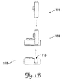
- FIGS 1A and 1B illustrate a 6-DOF MEMS sensor 100 of one embodiment of the present invention.
- Sensor 100 comprises a first wafer segment 110 having two accelerometers 120-1 and 120-2 oriented to measure accelerations on axes perpendicular with respect to each other, and two gyroscopes 125-1 and 125-2 oriented to measure motion on axes perpendicular with respect to each other.
- Sensor 100 further comprises a second wafer segment 115 assembled into a perpendicular orientation with first wafer segment 110.
- first wafer segment 110 includes a mounting trench 116 into which second wafer segment 115 is vertically inserted, as illustrated in Figure 1B.
- first wafer segment 110 and second wafer segment 115 are bonded together using a silicon fusion bonding or similar process.
- Second wafer segment 115 includes an accelerometer 120-3 oriented to measure accelerations on an axis perpendicular with respect to accelerometers 120-1 and 120-2, and a gyroscope 125-3 oriented to measure motion on an axis that is orthogonal with respect to gyroscopes 125-1 and 125-2.
- first and second wafer segments 110 and 115 respectively are electrically coupled together via contact bridges 127-1 and 127-2.
- the resultant 6-DOF MEMS sensor 100 is a set of inertial sensors comprising of mutually orthogonal accelerometers, 120-1, 120-2, 120-3 and mutually orthogonal gyroscopes 125-1, 125-2 and 125-3. 6-DOF MEMS sensor 100 is thus installable as a single sensor device package rather than as a triad of single axis sensors individually packaged and mounted.
- One advantage of sensor 100 is that the axes of accelerometers, 120-1 to 120-3 and gyroscopes 125-1 to 125-3 are inherently aligned with respect to each other to a high degree of precision afforded by integrated circuit manufacturing processes.
- triads of single axis sensors typically comprise single axis sensors mechanically mounted orthogonally on a separate bracket or housing, with the limited alignment precision inherent in such mechanical mountings.
- sensor 100 is effectively immune to internal alignment shifts due to thermal effects and ageing, unlike mechanically mounted single axis sensor triads.
- wafer segments such as wafer segments 110 and 115 are typically produced in bulk from larger silicon wafers.
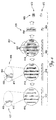
- Figures 2 and 3 illustrate one method for producing a wafer segment 110 of one embodiment of the present invention from such a larger silicon wafer 210.
- silicon wafer 210 comprises a plurality of accelerometer pairs 215-1 and 215-2 and gyroscope pairs 220-1 and 220-2 oriented as described with respect to wafer segment 110 of Figure 1.
- there are any number of ways of fabricating silicon wafer 210 as discussed in more detail below.
- Figure 3 is a flow chart illustrating a method for fabricating a first silicon wafer segment 110 from silicon wafer 210, of one embodiment of the present invention.
- the method begins at 310 with applying one or more contact bridges 240 (shown generally in Figure 2 at 206).
- contact bridges 240 comprise gold (Au) electroplating, or other similar electrical conducting material.
- one or more contact bridges 240 are applied for each of accelerometers pairs 215 and gyroscope pairs 220.
- applying contact bridges 240 comprises applying phosphorus-doped silicon dioxide (PSG) photoresist material deposited with a chemical-vapor deposition (CVD) and masking with lithography etching and sputter deposition.
- PSG phosphorus-doped silicon dioxide
- CVD chemical-vapor deposition
- the method proceeds at 320 with etching one or more mounting trenches 250 (shown generally in Figure 2 at 206).
- etching one or more mounting trenches 250 comprises masking with lithography and deep reactive ion etching (DRIE).
- the photoresist is removed using a hydrofluoric-acid (HF) etch followed by one or more de-ionized water soaks.
- the method continues at 330 with cutting and separating wafer 210 into cross sections 260 (shown generally in Figure 2 at 207 and 208) parallel to contact bridges 240.
- the method proceeds to 340 with cutting and separating cross sections 260 into individual wafer segments 270 (shown generally in Figure 2 at 209).
- Figures 4 and 5 illustrate one method for producing a second wafer segment 115 of one embodiment of the present invention from a larger silicon wafer 410.
- a silicon wafer 410 comprises a plurality of single axis accelerometers 415 and gyroscopes 420 as described with respect to wafer segment 115 of Figure 1.
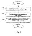
- Figure 5 is a flow chart illustrating a method for fabricating a second silicon wafer segment 115 from silicon wafer 410, of one embodiment of the present invention. The method begins at 510 with applying one or more contact bridges 440 (shown generally in Figure 4 at 406).
- contact bridges 440 comprise Au electroplating, or other similar electrical conducting material.
- one or more Au electroplating contact bridges is applied for each accelerometer 415 and gyroscope 420.
- applying contact bridges 440 is comprised of applying PSG photoresist with a CVD and masking with lithography etching and sputter deposition.
- the photoresist is removed using an HF etch followed by one or more de-ionized water soaks.
- the method continues at 520 with cutting and separating wafer 410 into cross sections 460 (shown generally in Figure 4 at 407 and 408) parallel to contact bridges 440.
- the method proceeds to 530 with cutting and separating cross sections 460 into individual wafer segments 470 (shown generally in Figure 4 at 409).
- a complete 6-DOF MEMS sensor such as sensor 100, is produced from wafer segments 270 and 470 as illustrated by the method presented by Figure 6.
- the method begins at 610 with assembling wafer segment 470 and wafer segment 270 into a single sensor as portrayed in Figure 1B.
- assembling the wafer segments is comprised of inserting wafer segment 470 vertically into mounting trench 250 of wafer segment 270 such that contact bridge 240 contacts contact bridge 440 and accelerometer pairs 215 and gyroscope pairs 220 are orthogonal in axis with accelerometer 415 and gyroscope 420, respectively.
- the method then proceeds to 620 with bonding wafer segment 270 to wafer segment 470.
- wafer segment 270 and wafer segment 470 are bonded together using a process such as, but not limited to, silicon fusion bonding.
- embodiments of the present invention are not so limited.
- embodiments of the present invention include wafer segments comprising any number of inertial sensors so long as the 6-DOF MEMS sensor comprises at least three orthogonally oriented sensors.
- a first wafer segment comprises four gyroscopes and two accelerometers and the second wafer segment comprises two gyroscopes and four accelerometers, so long as at least three of the accelerometers or at least three of the gyroscopes are orthogonally oriented with respect to each other.
- inertial sensors such as accelerometers 120-1 to 120-3 and gyroscopes 125-1 to 125-3 in wafer segments 110 and 115 of Figure 1A.
- accelerometers 120-1 to 120-3 are fabricated in wafer segments 110 and 115 using the Honeywell, Inc. capacitive pendulous accelerometer design and HIMEMS process.
- gyroscopes 125-1 to 125-3 are fabricated onto wafer segments 110 and 115 using the vibratory-rate gyroscope designed by Morgan Research Corp. in conjunction with the U.S. Army Aviation and Missile Command and The Aegis Technologies Group.
- these accelerometer and gyroscope designs are compatible with each other such that they can be manufactured in the same process in order to fabricate them on the same silicon wafer.
Landscapes
- Physics & Mathematics (AREA)
- General Physics & Mathematics (AREA)
- Engineering & Computer Science (AREA)
- Microelectronics & Electronic Packaging (AREA)
- Computer Hardware Design (AREA)
- Gyroscopes (AREA)
- Micromachines (AREA)
- Pressure Sensors (AREA)
Abstract
Description
- Fabrication of micro electro-mechanical systems (MEMS) is being refined every day, creating a multitude of single-axis sensors. Multi-axis sensors are currently production limited to 2-axis with the optimal 3-axis design efficiently unattainable for measuring 6 degrees of freedom (6-DOF). Although inertial measurement units (IMUs) are available that provide 6-DOF capability, they are composed of multiple individual sensors assembled in a 3-axis triad. Inherently, misalignment errors result from even minor imperfections during this assembly process. Additionally, as IMUs today are constructed from multiple individual accelerometers and gyros, their implementation methods are more expensive and error prone.
- For the reasons stated above and for other reasons stated below which will become apparent to those skilled in the art upon reading and understanding the specification, there is a need in the art for techniques of reducing misalignment errors in micro electro-mechanical systems.
- The Embodiments of the present invention provide methods and systems for 3-axis MEMS sensor systems and methods and will be understood by reading and studying the following specification.
- In one embodiment, a six degree of freedom inertial sensor is provided. The sensor comprises a first silicon wafer segment having at least one inertial sensor pair; a second silicon wafer segment having at least one inertial sensor; wherein the at least one inertial sensor pair comprises one or both of an accelerometer pair and a gyroscope pair; wherein the at least one inertial sensor comprises one or both of an accelerometer and a gyroscope; and wherein the first silicon wafer segment and the second silicon wafer segment are bonded together such the at least one inertial sensor pair and the at least one inertial sensor are orientated orthogonal to each other.
- In another embodiment, a method for producing a six degree of freedom inertial sensor is provided. The method comprises fabricating a first silicon wafer segment having at least one inertial sensor pair, wherein the at least one inertial sensor pair comprises one or both of a pair of orthogonally oriented accelerometers and a pair of orthogonally oriented gyroscopes; fabricating a second silicon wafer segment having at least one inertial sensor, wherein the at least one inertial sensor comprises one or both of an accelerometer and a gyroscope; assembling together the first silicon wafer segment and the second silicon wafer segment, wherein the first silicon wafer segment and the second silicon wafer are assembled together such that the at least one inertial sensor pair and the at least one inertial sensor are oriented orthogonal to each other; and bonding the first silicon wafer segment to the second silicon wafer segment.
- In yet another embodiment, a six degree of freedom inertial sensor is provided. The sensor comprises means for detecting one or both of acceleration and motion in a direction of a first axis; means for detecting one or both of acceleration and motion in a direction of a second access orthogonal with the first axis; means for detecting one or both of acceleration and motion in a direction of a third axis orthogonal with the first axis and the second axis; wherein the means for detecting one or both of acceleration and motion in a direction of a first axis and the means for detecting one or both of acceleration and motion in a direction of a second access are located on a first silicon wafer means and the means for detecting one or both of acceleration and motion in a direction of a third axis is located on a second silicon wafer means; and means for bonding the first silicon wafer means to the second silicon wafer means.
- Embodiments of the present invention can be more easily understood and further advantages and uses thereof more readily apparent, when considered in view of the description of the preferred embodiments and the following figures in which:
- Figures 1A and 1B are illustrations of one embodiment of an inertial sensor.
- Figure 2 is an illustration of one embodiment of production of a first silicon wafer segment.
- Figure 3 is a flow chart of one embodiment of a method for producing a first silicon wafer segment.
- Figure 4 is an illustration of one embodiment of production of a second silicon wafer segment of one embodiment of the present invention.
- Figure 5 is a flow chart of one embodiment of a method for producing a second silicon wafer segment.
- Figure 6 is a flow chart of one embodiment of a method for producing a six degree of freedom inertial sensor from a first silicon wafer segment and a second silicon wafer segment.
- In accordance with common practice, the various described features are not drawn to scale but are drawn to emphasize features relevant to the present invention. Reference characters denote like elements throughout figures and text.
- In the following detailed description, reference is made to the accompanying drawings that form a part hereof, and in which is shown by way of specific illustrative embodiments in which the invention may be practiced. These embodiments are described in sufficient detail to enable those skilled in the art to practice the invention, and it is to be understood that other embodiments may be utilized and that logical, mechanical and electrical changes may be made without departing from the scope of the present invention. The following detailed description is, therefore, not to be taken in a limiting sense.
- Embodiments of the present invention provide system and methods to reduce misalignment errors, as well as the cost of producing MEMS inertial sensors for use in applications such as, but not limited to, commercial, military and space applications. Embodiments of the present invention exploit the benefits of producing multiple sensors on silicon wafers, using extremely accurate, and currently available integrated circuit and MEMS fabrication methods. By producing multiple sensors on a chip, the cost of development is vastly reduced, permitting the use of this technology in broad markets. Because fabrication methods presented by embodiments of the present invention are very precise, a reduction in sensor error cross-coupling and misalignment is achieved. The resulting improvements in overall IMU sensor performance results in both cheaper and more accurate 6-DOF sensors.
- Embodiments of the present invention utilize current accelerometer and gyroscope designs in a homogeneous micro-fabrication process to fabricate both accelerometers and gyroscopes on the same silicon wafers. After fabricating both accelerometers and gyroscopes on two single wafers, embodiments of the present invention provide methods to cut and bond the two wafers to generate a third sensor axis for an all attitude inertial navigation solution. The result is a single 6-DOF MEMS sensor that is both cheaper and more accurate than 6-DOF sensors available in the art today.
- Figures 1A and 1B illustrate a 6-
DOF MEMS sensor 100 of one embodiment of the present invention.Sensor 100 comprises afirst wafer segment 110 having two accelerometers 120-1 and 120-2 oriented to measure accelerations on axes perpendicular with respect to each other, and two gyroscopes 125-1 and 125-2 oriented to measure motion on axes perpendicular with respect to each other.Sensor 100 further comprises asecond wafer segment 115 assembled into a perpendicular orientation withfirst wafer segment 110. In one embodiment,first wafer segment 110 includes amounting trench 116 into whichsecond wafer segment 115 is vertically inserted, as illustrated in Figure 1B. In one embodiment,first wafer segment 110 andsecond wafer segment 115 are bonded together using a silicon fusion bonding or similar process.Second wafer segment 115 includes an accelerometer 120-3 oriented to measure accelerations on an axis perpendicular with respect to accelerometers 120-1 and 120-2, and a gyroscope 125-3 oriented to measure motion on an axis that is orthogonal with respect to gyroscopes 125-1 and 125-2. In one embodiment, first andsecond wafer segments DOF MEMS sensor 100 is a set of inertial sensors comprising of mutually orthogonal accelerometers, 120-1, 120-2, 120-3 and mutually orthogonal gyroscopes 125-1, 125-2 and 125-3. 6-DOF MEMS sensor 100 is thus installable as a single sensor device package rather than as a triad of single axis sensors individually packaged and mounted. One advantage ofsensor 100 is that the axes of accelerometers, 120-1 to 120-3 and gyroscopes 125-1 to 125-3 are inherently aligned with respect to each other to a high degree of precision afforded by integrated circuit manufacturing processes. In contrast, triads of single axis sensors typically comprise single axis sensors mechanically mounted orthogonally on a separate bracket or housing, with the limited alignment precision inherent in such mechanical mountings. In addition,sensor 100 is effectively immune to internal alignment shifts due to thermal effects and ageing, unlike mechanically mounted single axis sensor triads. - One skilled in the art would recognize that wafer segments, such as
wafer segments wafer segment 110 of one embodiment of the present invention from such alarger silicon wafer 210. Shown generally at 205 in Figure 2, in one embodiment,silicon wafer 210 comprises a plurality of accelerometer pairs 215-1 and 215-2 and gyroscope pairs 220-1 and 220-2 oriented as described with respect towafer segment 110 of Figure 1. As would be appreciated by one skilled in the art upon reading this specification, there are any number of ways of fabricatingsilicon wafer 210, as discussed in more detail below. Figure 3 is a flow chart illustrating a method for fabricating a firstsilicon wafer segment 110 fromsilicon wafer 210, of one embodiment of the present invention. The method begins at 310 with applying one or more contact bridges 240 (shown generally in Figure 2 at 206). In one embodiment,contact bridges 240 comprise gold (Au) electroplating, or other similar electrical conducting material. In one embodiment, one ormore contact bridges 240 are applied for each of accelerometers pairs 215 and gyroscope pairs 220. In one embodiment, applyingcontact bridges 240 comprises applying phosphorus-doped silicon dioxide (PSG) photoresist material deposited with a chemical-vapor deposition (CVD) and masking with lithography etching and sputter deposition. In one embodiment, the method proceeds at 320 with etching one or more mounting trenches 250 (shown generally in Figure 2 at 206). In one embodiment, etching one ormore mounting trenches 250 comprises masking with lithography and deep reactive ion etching (DRIE). In one embodiment, the photoresist is removed using a hydrofluoric-acid (HF) etch followed by one or more de-ionized water soaks. In one embodiment, the method continues at 330 with cutting and separatingwafer 210 into cross sections 260 (shown generally in Figure 2 at 207 and 208) parallel tocontact bridges 240. In one embodiment, the method proceeds to 340 with cutting and separatingcross sections 260 into individual wafer segments 270 (shown generally in Figure 2 at 209). - Figures 4 and 5 illustrate one method for producing a
second wafer segment 115 of one embodiment of the present invention from alarger silicon wafer 410. Shown generally at 405 in Figure 4 in one embodiment, asilicon wafer 410 comprises a plurality ofsingle axis accelerometers 415 andgyroscopes 420 as described with respect towafer segment 115 of Figure 1. Figure 5 is a flow chart illustrating a method for fabricating a secondsilicon wafer segment 115 fromsilicon wafer 410, of one embodiment of the present invention. The method begins at 510 with applying one or more contact bridges 440 (shown generally in Figure 4 at 406). In one embodiment,contact bridges 440 comprise Au electroplating, or other similar electrical conducting material. In one embodiment, one or more Au electroplating contact bridges is applied for eachaccelerometer 415 andgyroscope 420. In one embodiment, applyingcontact bridges 440 is comprised of applying PSG photoresist with a CVD and masking with lithography etching and sputter deposition. In one embodiment, the photoresist is removed using an HF etch followed by one or more de-ionized water soaks. In one embodiment, the method continues at 520 with cutting and separatingwafer 410 into cross sections 460 (shown generally in Figure 4 at 407 and 408) parallel to contactbridges 440. In one embodiment, the method proceeds to 530 with cutting and separatingcross sections 460 into individual wafer segments 470 (shown generally in Figure 4 at 409). - A complete 6-DOF MEMS sensor, such as
sensor 100, is produced fromwafer segments wafer segment 470 andwafer segment 270 into a single sensor as portrayed in Figure 1B. In one embodiment, assembling the wafer segments is comprised of insertingwafer segment 470 vertically into mountingtrench 250 ofwafer segment 270 such thatcontact bridge 240contacts contact bridge 440 and accelerometer pairs 215 and gyroscope pairs 220 are orthogonal in axis withaccelerometer 415 andgyroscope 420, respectively. The method then proceeds to 620 withbonding wafer segment 270 towafer segment 470. In one embodiment,wafer segment 270 andwafer segment 470 are bonded together using a process such as, but not limited to, silicon fusion bonding. - Although this specification provides illustrative descriptions of a 6-DOF MEMS sensor having two accelerometers and two gyroscopes on one wafer segment, and one accelerometer and one gyroscope on the other, embodiments of the present invention are not so limited. To the contrary, embodiments of the present invention include wafer segments comprising any number of inertial sensors so long as the 6-DOF MEMS sensor comprises at least three orthogonally oriented sensors. For example, in an alternate embodiment a first wafer segment comprises four gyroscopes and two accelerometers and the second wafer segment comprises two gyroscopes and four accelerometers, so long as at least three of the accelerometers or at least three of the gyroscopes are orthogonally oriented with respect to each other.
- As would be appreciated by one skilled in the art upon reading this specification, there exist a number of techniques available for fabricating inertial sensors such as accelerometers 120-1 to 120-3 and gyroscopes 125-1 to 125-3 in
wafer segments wafer segments wafer segments - Although specific embodiments have been illustrated and described herein, it will be appreciated by those of ordinary skill in the art that any arrangement, which is calculated to achieve the same purpose, may be substituted for the specific embodiment shown. This application is intended to cover any adaptations or variations of the present invention. Therefore, it is manifestly intended that this invention be limited only by the claims and the equivalents thereof.
Claims (10)
- A method for producing a six degree of freedom inertial sensor, the method comprising:fabricating a first silicon wafer segment (110) having at least one inertial sensor pair (120-1,2, 125-1,2), wherein the at least one inertial sensor pair (120-1,120-2, 125-1,120-2) comprises one or both of a pair of orthogonally oriented accelerometers (120-1,120-2) and a pair of orthogonally oriented gyroscopes (125-1,120-2);fabricating a second silicon wafer segment (115) (115) having at least one inertial sensor (120-3, 125-3), wherein the at least one inertial sensor comprises one or both of an accelerometer (120-3) and a gyroscope (125-3);assembling together the first silicon wafer segment (110) and the second silicon wafer segment (115), wherein the first silicon wafer segment (110) and the second silicon wafer are assembled together such that the at least one inertial sensor pair (120-1,120-2, 125-1,120-2) and the at least one inertial sensor (120-3, 125-3) are oriented orthogonal to each other; andbonding the first silicon wafer segment (110) to the second silicon wafer segment (115).
- The method of claim 1, wherein assembling the first silicon wafer segment (110) with the second silicon wafer segment (115) further comprises one of:inserting the first silicon wafer segment (110) into a mounting trench (116) within the second silicon wafer segment (115); andinserting the second silicon wafer segment (115) into a mounting trench (116) within the first silicon wafer segment (110).
- The method of claim 1, wherein bonding the first silicon wafer segment (110) to the second silicon wafer segment (115) further comprises silicon fusion bonding.
- The method of claim 1, wherein fabricating the first silicon wafer segment (110) comprises:fabricating a first silicon wafer (210) having one or both of a plurality of orthogonal accelerometers pairs (215-1, 215-2) and a plurality of orthogonal gyroscope pairs (220-1, 220-2);applying a plurality of contact bridges (240) to the first silicon wafer (210);etching one or more mounting trenches (116, 250) into the first silicon wafer (210);cutting the first silicon wafer (210) into one or more cross sections (260) parallel to the contact bridges (240); andseparating the one or more cross sections (260) into one or more wafer segments (270).
- The method of claim 4, wherein applying a plurality of contact bridges (240) to the first silicon wafer (210) comprises:applying a plurality of gold electroplating contact bridges (240) to the first silicon wafer (210).
- The method of claim 5, wherein applying a plurality of gold electroplating contact bridges (240) to the first silicon wafer (210) further comprises:applying PSG photoresist deposited with a CVD;masking with lithography etching and sputter deposition;removing PSG photoresist with HF etch; andsoaking the first silicon wafer (210) in de-ionized water.
- The method of claim 4, wherein etching one or more mounting trenches (116, 250) comprises:masking with lithography and deep reactive ion etching.
- The method of claim 1, wherein fabricating the second silicon wafer segment (115) comprises:fabricating a second silicon wafer (410) having one or both of a plurality of accelerometers (415-1) and a plurality of gyroscopes (420);applying a plurality of contact bridges (440) to the second silicon wafer (410);cutting the second silicon wafer (410) into one or more cross sections (460) parallel to the contact bridges (440); andseparating the one or more cross sections (460) into one or more wafer segments (470).
- The method of claim 8, wherein applying a plurality of contact bridges (440) to the second silicon wafer (410) comprises:applying a plurality of gold electroplating contact bridges (440) to the second silicon wafer (410).
- The method of claim 9, wherein applying a plurality of gold electroplating contact bridges (440) to the second silicon wafer (410) further comprises:applying PSG photoresist deposited with a CVD;masking with lithography etching and sputter deposition;removing PSG photoresist with HF etch; andsoaking the silicon wafer in de-ionized water.
Applications Claiming Priority (1)
| Application Number | Priority Date | Filing Date | Title |
|---|---|---|---|
| US11/260,817 US7237437B1 (en) | 2005-10-27 | 2005-10-27 | MEMS sensor systems and methods |
Publications (2)
| Publication Number | Publication Date |
|---|---|
| EP1780175A2 true EP1780175A2 (en) | 2007-05-02 |
| EP1780175A3 EP1780175A3 (en) | 2008-05-07 |
Family
ID=37711283
Family Applications (1)
| Application Number | Title | Priority Date | Filing Date |
|---|---|---|---|
| EP06122979A Withdrawn EP1780175A3 (en) | 2005-10-27 | 2006-10-26 | Method for assembling MEMS parts |
Country Status (6)
| Country | Link |
|---|---|
| US (1) | US7237437B1 (en) |
| EP (1) | EP1780175A3 (en) |
| JP (1) | JP2007121304A (en) |
| KR (1) | KR20070046001A (en) |
| AU (1) | AU2006233224A1 (en) |
| CA (1) | CA2565752A1 (en) |
Cited By (1)
| Publication number | Priority date | Publication date | Assignee | Title |
|---|---|---|---|---|
| WO2009129066A2 (en) | 2008-04-14 | 2009-10-22 | Honeywell International Inc. | Method and system for forming an electronic assembly having inertial sensors mounted thereto |
Families Citing this family (25)
| Publication number | Priority date | Publication date | Assignee | Title |
|---|---|---|---|---|
| US7253079B2 (en) * | 2002-05-09 | 2007-08-07 | The Charles Stark Draper Laboratory, Inc. | Coplanar mounting member for a MEM sensor |
| TW200813431A (en) * | 2006-08-09 | 2008-03-16 | Hitachi Metals Ltd | Multi-range three-axis acceleration sensor device |
| US20090262074A1 (en) * | 2007-01-05 | 2009-10-22 | Invensense Inc. | Controlling and accessing content using motion processing on mobile devices |
| US20090265671A1 (en) * | 2008-04-21 | 2009-10-22 | Invensense | Mobile devices with motion gesture recognition |
| US8250921B2 (en) | 2007-07-06 | 2012-08-28 | Invensense, Inc. | Integrated motion processing unit (MPU) with MEMS inertial sensing and embedded digital electronics |
| US8141424B2 (en) * | 2008-09-12 | 2012-03-27 | Invensense, Inc. | Low inertia frame for detecting coriolis acceleration |
| US8462109B2 (en) * | 2007-01-05 | 2013-06-11 | Invensense, Inc. | Controlling and accessing content using motion processing on mobile devices |
| US8047075B2 (en) * | 2007-06-21 | 2011-11-01 | Invensense, Inc. | Vertically integrated 3-axis MEMS accelerometer with electronics |
| US8952832B2 (en) | 2008-01-18 | 2015-02-10 | Invensense, Inc. | Interfacing application programs and motion sensors of a device |
| US8508039B1 (en) | 2008-05-08 | 2013-08-13 | Invensense, Inc. | Wafer scale chip scale packaging of vertically integrated MEMS sensors with electronics |
| US7934423B2 (en) | 2007-12-10 | 2011-05-03 | Invensense, Inc. | Vertically integrated 3-axis MEMS angular accelerometer with integrated electronics |
| US20100071467A1 (en) * | 2008-09-24 | 2010-03-25 | Invensense | Integrated multiaxis motion sensor |
| US8020441B2 (en) * | 2008-02-05 | 2011-09-20 | Invensense, Inc. | Dual mode sensing for vibratory gyroscope |
| JP4755137B2 (en) | 2007-05-01 | 2011-08-24 | 株式会社エヌ・ティ・ティ・ドコモ | Base station apparatus and communication control method |
| RU2377576C1 (en) * | 2008-08-12 | 2009-12-27 | Открытое акционерное общество "Московский институт электромеханики и автоматики" | Three-axis micro-mechanic gauge of motion parametres |
| JP2011133246A (en) * | 2009-12-22 | 2011-07-07 | Sony Corp | Angular velocity sensor and electronic apparatus |
| WO2011144883A1 (en) * | 2010-05-19 | 2011-11-24 | Salisbury Nhs Foundation Trust | Accelerometer assembly and the use thereof |
| US8306676B1 (en) | 2011-04-15 | 2012-11-06 | Honeywell International Inc. | Systems and methods for differential altitude estimation utilizing spatial interpolation of pressure sensor data |
| US8316552B1 (en) | 2011-05-05 | 2012-11-27 | Honeywell International Inc. | Systems and methods for three-axis sensor chip packages |
| US8459112B2 (en) | 2011-06-09 | 2013-06-11 | Honeywell International Inc. | Systems and methods for three dimensional sensors |
| US8640552B2 (en) | 2011-09-06 | 2014-02-04 | Honeywell International Inc. | MEMS airflow sensor die incorporating additional circuitry on the die |
| ITVR20110210A1 (en) * | 2011-11-24 | 2013-05-25 | Cefriel Societa Consortile A Respon Sabilita Limit | IMPACT DETECTION DEVICE. |
| US8957355B1 (en) * | 2012-01-26 | 2015-02-17 | The Boeing Company | Inertial measurement unit apparatus for use with guidance systems |
| CN103234442B (en) * | 2013-04-17 | 2015-05-27 | 吉林大学 | Device for measuring six degrees of freedom of platform |
| SE538872C2 (en) * | 2015-05-04 | 2017-01-17 | Lkab Wassara Ab | Gyro-based surveying tool and method for surveying |
Family Cites Families (8)
| Publication number | Priority date | Publication date | Assignee | Title |
|---|---|---|---|---|
| GB2146776B (en) * | 1983-09-16 | 1986-07-30 | Ferranti Plc | Accelerometer systems |
| FR2608771B1 (en) * | 1986-12-18 | 1989-04-28 | Onera (Off Nat Aerospatiale) | ULTRASENSITIVE ACCELEROMETER CALIBRATION DEVICE |
| GB9507930D0 (en) * | 1995-04-19 | 1995-06-14 | Smiths Industries Plc | Inertial sensor assemblies |
| DE19720106C2 (en) * | 1997-05-16 | 2001-03-15 | Telefunken Microelectron | Device for receiving electrical components |
| US6128955A (en) * | 1999-07-09 | 2000-10-10 | Mimura; Nobuharu | Method for measuring 6 degrees of freedom motion and device therefor |
| US6876926B2 (en) * | 2002-09-26 | 2005-04-05 | Honeywell International Inc. | Method and system for processing pulse signals within an inertial navigation system |
| US7040922B2 (en) * | 2003-06-05 | 2006-05-09 | Analog Devices, Inc. | Multi-surface mounting member and electronic device |
| DE102005023591A1 (en) * | 2005-05-18 | 2006-11-30 | Hl-Planar Technik Gmbh | Field measuring device, measuring module for a field measuring device and method of production for a plurality of measuring modules |
-
2005
- 2005-10-27 US US11/260,817 patent/US7237437B1/en not_active Expired - Fee Related
-
2006
- 2006-10-26 EP EP06122979A patent/EP1780175A3/en not_active Withdrawn
- 2006-10-26 CA CA002565752A patent/CA2565752A1/en not_active Abandoned
- 2006-10-27 KR KR1020060105155A patent/KR20070046001A/en not_active Withdrawn
- 2006-10-27 JP JP2006292808A patent/JP2007121304A/en not_active Withdrawn
- 2006-10-27 AU AU2006233224A patent/AU2006233224A1/en not_active Abandoned
Cited By (2)
| Publication number | Priority date | Publication date | Assignee | Title |
|---|---|---|---|---|
| WO2009129066A2 (en) | 2008-04-14 | 2009-10-22 | Honeywell International Inc. | Method and system for forming an electronic assembly having inertial sensors mounted thereto |
| EP2269000A4 (en) * | 2008-04-14 | 2011-11-23 | Honeywell Int Inc | Method and system for forming an electronic assembly having inertial sensors mounted thereto |
Also Published As
| Publication number | Publication date |
|---|---|
| CA2565752A1 (en) | 2007-04-27 |
| AU2006233224A1 (en) | 2007-05-17 |
| US7237437B1 (en) | 2007-07-03 |
| JP2007121304A (en) | 2007-05-17 |
| EP1780175A3 (en) | 2008-05-07 |
| KR20070046001A (en) | 2007-05-02 |
Similar Documents
| Publication | Publication Date | Title |
|---|---|---|
| US7237437B1 (en) | MEMS sensor systems and methods | |
| US6796179B2 (en) | Split-resonator integrated-post MEMS gyroscope | |
| US6105427A (en) | Micro-mechanical semiconductor accelerometer | |
| US7878060B2 (en) | Motion sensor and method of manufacturing the same | |
| CN115494261B (en) | Inertial sensors and inertial measurement devices | |
| US8656778B2 (en) | In-plane capacitive mems accelerometer | |
| US8122767B2 (en) | D'arsonval movement mems accelerometer | |
| US20200064134A1 (en) | Micromechanical detection structure for a mems sensor device, in particular a mems gyroscope, with improved driving features | |
| KR20050086918A (en) | Methods and systems for decelarating proof mass movements within mems structures | |
| CN113494908B (en) | MEMS inertial sensors, inertial measurement units and inertial navigation systems | |
| US7069784B1 (en) | Pendulous in-plane MEMS accelerometer device | |
| EP1711836A1 (en) | Coplanar proofmasses employable to sense acceleration along three axes | |
| CN104237562A (en) | Angular rate sensor with quadrature error compensation | |
| CN115754349B (en) | Sensors and electronics | |
| CN117452023A (en) | Physical quantity sensors and inertial measurement devices | |
| US20230349945A1 (en) | Inertial sensor and inertial measurement unit | |
| US9731958B2 (en) | Microelectromechanical system and fabricating process having decoupling structure that includes attaching element for fastening to carrier | |
| US11573246B2 (en) | Inertial sensor and inertial measurement unit | |
| JP2014215294A (en) | MEMS element | |
| US7516661B2 (en) | Z offset MEMS device | |
| CN114057154B (en) | MEMS devices | |
| US11802889B2 (en) | Inertial sensor and inertial measurement device | |
| KR20060124267A (en) | Planar triaxial inertial measurement system without misalignment | |
| JP7852429B2 (en) | Physical quantity sensors and inertial measurement devices | |
| JP2005300163A (en) | 3-axis rate gyro |
Legal Events
| Date | Code | Title | Description |
|---|---|---|---|
| PUAI | Public reference made under article 153(3) epc to a published international application that has entered the european phase |
Free format text: ORIGINAL CODE: 0009012 |
|
| AK | Designated contracting states |
Kind code of ref document: A2 Designated state(s): AT BE BG CH CY CZ DE DK EE ES FI FR GB GR HU IE IS IT LI LT LU LV MC NL PL PT RO SE SI SK TR |
|
| AX | Request for extension of the european patent |
Extension state: AL BA HR MK YU |
|
| PUAL | Search report despatched |
Free format text: ORIGINAL CODE: 0009013 |
|
| AK | Designated contracting states |
Kind code of ref document: A3 Designated state(s): AT BE BG CH CY CZ DE DK EE ES FI FR GB GR HU IE IS IT LI LT LU LV MC NL PL PT RO SE SI SK TR |
|
| AX | Request for extension of the european patent |
Extension state: AL BA HR MK RS |
|
| AKX | Designation fees paid | ||
| REG | Reference to a national code |
Ref country code: DE Ref legal event code: 8566 |
|
| STAA | Information on the status of an ep patent application or granted ep patent |
Free format text: STATUS: THE APPLICATION IS DEEMED TO BE WITHDRAWN |
|
| 18D | Application deemed to be withdrawn |
Effective date: 20081108 |