EP1779513B1 - Enhanced passgate structures for reducing leakage current - Google Patents
Enhanced passgate structures for reducing leakage current Download PDFInfo
- Publication number
- EP1779513B1 EP1779513B1 EP05778119A EP05778119A EP1779513B1 EP 1779513 B1 EP1779513 B1 EP 1779513B1 EP 05778119 A EP05778119 A EP 05778119A EP 05778119 A EP05778119 A EP 05778119A EP 1779513 B1 EP1779513 B1 EP 1779513B1
- Authority
- EP
- European Patent Office
- Prior art keywords
- passgate
- voltage
- integrated circuit
- transistors
- circuit defined
- Prior art date
- Legal status (The legal status is an assumption and is not a legal conclusion. Google has not performed a legal analysis and makes no representation as to the accuracy of the status listed.)
- Expired - Lifetime
Links
Images




Classifications
-
- H—ELECTRICITY
- H03—ELECTRONIC CIRCUITRY
- H03K—PULSE TECHNIQUE
- H03K19/00—Logic circuits, i.e. having at least two inputs acting on one output; Inverting circuits
- H03K19/02—Logic circuits, i.e. having at least two inputs acting on one output; Inverting circuits using specified components
- H03K19/173—Logic circuits, i.e. having at least two inputs acting on one output; Inverting circuits using specified components using elementary logic circuits as components
- H03K19/177—Logic circuits, i.e. having at least two inputs acting on one output; Inverting circuits using specified components using elementary logic circuits as components arranged in matrix form
- H03K19/1778—Structural details for adapting physical parameters
-
- H—ELECTRICITY
- H03—ELECTRONIC CIRCUITRY
- H03K—PULSE TECHNIQUE
- H03K19/00—Logic circuits, i.e. having at least two inputs acting on one output; Inverting circuits
- H03K19/02—Logic circuits, i.e. having at least two inputs acting on one output; Inverting circuits using specified components
- H03K19/173—Logic circuits, i.e. having at least two inputs acting on one output; Inverting circuits using specified components using elementary logic circuits as components
- H03K19/177—Logic circuits, i.e. having at least two inputs acting on one output; Inverting circuits using specified components using elementary logic circuits as components arranged in matrix form
- H03K19/1778—Structural details for adapting physical parameters
- H03K19/17784—Structural details for adapting physical parameters for supply voltage
-
- H—ELECTRICITY
- H03—ELECTRONIC CIRCUITRY
- H03K—PULSE TECHNIQUE
- H03K19/00—Logic circuits, i.e. having at least two inputs acting on one output; Inverting circuits
- H03K19/02—Logic circuits, i.e. having at least two inputs acting on one output; Inverting circuits using specified components
- H03K19/173—Logic circuits, i.e. having at least two inputs acting on one output; Inverting circuits using specified components using elementary logic circuits as components
- H03K19/177—Logic circuits, i.e. having at least two inputs acting on one output; Inverting circuits using specified components using elementary logic circuits as components arranged in matrix form
- H03K19/1778—Structural details for adapting physical parameters
- H03K19/17792—Structural details for adapting physical parameters for operating speed
Definitions
- NMOS passgate acts as an "open” or a "closed” switch.
- Document US 2003/05335 relates to structures and methods for selectively applying a well bias to only those portions of a PLD where such a bias is necessary or desirable, e.g., applying a positive well bias to transistors on critical paths within a user's design.
- a substrate for an integrated circuit includes a plurality of wells, each of which can be independently and programmably biased with the same or a different well bias voltage.
- FPGA implementation software automatically determines the critical paths and generates a configuration bitstream that enables positive well biasing only for the transistors participating in the critical paths, or only for programmable logic elements (e.g., CLBs or lookup tables) containing those transistors.
- negative well biasing is selectively applied to reduce leakage current.
- FIG. 3 is a simplified illustration of an aspect of another integrated circuit device which may be fabricated in accordance with the principles of the present invention.
- FIG. 9 illustrates another aspect of the programmable logic device of FIG. 7 may be improved in accordance with the principles of the present invention.
- the passgate activation voltage may also be generated by any of a variety of voltage boosting/conversion circuitry such as charge pumps and voltage converters (e.g., DC/DC, AC/DC, etc.).
- the passgate activation voltage may be provided by a memory cell such as an SRAM-cell.
- FIG. 3 shows a portion of an integrated circuit device 30, which is divided into different sections 301/302/303, wherein all the transistors within a given section have been fabricated with a specific threshold voltage that may be different from that of the transistors in the other sections.
- sections 301 and 302 may each be a routing network with a high concentration of passgates (which may be used to construct, for example, interconnection switches and multiplexers). Accordingly, the transistors in sections 301 and 302 could be fabricated with a V T that is higher than that of the transistors in other sections 303.
- a triple-well process may be used to allow p-well 405 to be biased separately from the p-substrate 520, thereby allowing the V T of NMOS passgate 400 to be adjusted as a function of the source-to-bulk potential difference, V SB , which, in the arrangement shown in FIG. 5 , is dependent on V BIAS .
- FIG. 10 shows a portion of an integrated circuit 1000 employing the use of memory cells 1010 to drive passgate transistors 700/900 according to the principles of the present invention.
- Memory cells 1010 may be configurable ram cells such as SRAM cells.
- Passgate transistors 700/900 may be any of the enhanced passgate structures that have been described in the foregoing.
- Soft-error occurs when the logic state being stored in the memory cell inadvertently changes.
- Soft-error can be caused by, for example, sub-atomic particles (sometimes referred to as alpha particles or neutron beams) that disrupt the operation of silicon by changing the charge of the memory cell.
- Soft-error can also be caused by cross-coupling of memory cells.
- supply voltages e.g., nominal voltages
- Vccx as opposed to a nominal voltage, provides a supply voltage that enables memory cells 1010 to operate with a relatively low soft-error-rate.
Landscapes
- Physics & Mathematics (AREA)
- Mathematical Physics (AREA)
- Engineering & Computer Science (AREA)
- Computer Hardware Design (AREA)
- Computing Systems (AREA)
- General Engineering & Computer Science (AREA)
- Semiconductor Integrated Circuits (AREA)
- Design And Manufacture Of Integrated Circuits (AREA)
- Logic Circuits (AREA)
- Junction Field-Effect Transistors (AREA)
- Metal-Oxide And Bipolar Metal-Oxide Semiconductor Integrated Circuits (AREA)
- Static Random-Access Memory (AREA)
Abstract
Description
- This invention relates to integrated circuit devices, and more particularly to the passgate structures that may be used in such devices.
- One of the most ubiquitous structures within an integrated circuit device is the single-transistor passgate, which is commonly used to implement (either singly or in combination with other circuits) switches, multiplexers, logic functions (e.g., pass transistor logic), and gating mechanisms for tristatable circuits (e.g., buffers and drivers). In some integrated circuit devices, single-transistor passgate structures may account for a significant portion of the circuitry; for example, in the case of programmable logic devices, single-transistor passgates are used extensively throughout the device as part of the programmable interconnection circuitry.
- The operation of a typical single-transistor passgate may be succinctly illustrated by a description of an NMOS passgate (analogous principles of operation, as understood by one skilled in the art, would apply for a PMOS passgate). Depending on whether the potential difference between its gate terminal, VGATE, and its source terminal, VSOURCE, exceeds the threshold voltage, VT, a NMOS passgate acts as an "open" or a "closed" switch. (As is well-known in the art, there is no physical difference between the "source" and "drain" terminals of a MOS device; the source terminal of a NMOS transistor is the terminal having the lower voltage.) When VGATE-VSOURCE is less than VT, the NMOS passgate is in the "cutoff" state, thereby acting as an "open" switch; when VGATE-VSOURCE is greater than VT, the NMOS passgate is in the conduction state, thereby acting as a "closed" switch.
- As is well-known in the art, VT is not a discrete value for an MOS transistor; it may be considered a range of values that is influenced by a variety of second-order effects, such as substrate bias and subthreshold conduction. However, in order to simplify the illustration of the principles of the present invention, VT will be discussed herein as if it is a discrete value rather than a range of values.
- With the current trend in scaling down device geometries (e.g., 0.18µm process down to 0.13µm, 90nm, and lower) and the consequent use of ever-lower operating voltages (e.g., supply voltages, bias voltages, etc.), which are nearing levels comparable to VT, the ability of transistor passgate structures to function at relatively high speeds while at the same time minimizing leakage current is a difficult design hurdle to overcome.
- Moreover, this trend of smaller device geometries and consequent use of lower operating voltages is creating a design tradeoff between speed (e.g., response time for the passgate transistor to turn ON) and leakage current (e.g., the current that passes through the passgate transistor when turned OFF) that was not previously experienced with larger device geometries and the consequent use of higher operating voltages. That is, if conventional design techniques are applied to smaller device geometries, high speed passgate operation is accompanied with high leakage current, whereas low leakage current is accompanied with low speed passgate operation. High leakage current is undesirable because it results in excess heat, power loss, and poorer performance.
- Another problem associated with shrinking geometries is the consequent use of lower operating voltages. This lower operating voltage is typically a nominal voltage supplied to the integrated circuitry, and may be insufficient for certain circuitry, such as configurable memory cells (e.g., SRAM) within the integrated circuitry, to operate properly. For example, as the supply voltage decreases, the soft-error-rate increases because the critical charge needed to flip the cells (from one logic state to another) is reduced.
- Document
US 2003/05335 relates to structures and methods for selectively applying a well bias to only those portions of a PLD where such a bias is necessary or desirable, e.g., applying a positive well bias to transistors on critical paths within a user's design. A substrate for an integrated circuit includes a plurality of wells, each of which can be independently and programmably biased with the same or a different well bias voltage. In one embodiment, FPGA implementation software automatically determines the critical paths and generates a configuration bitstream that enables positive well biasing only for the transistors participating in the critical paths, or only for programmable logic elements (e.g., CLBs or lookup tables) containing those transistors. In another embodiment, negative well biasing is selectively applied to reduce leakage current. - Document
US 2003/071681 relates to an IC device having a MOSFET serving as a power switch, a condenser connected between a first input terminal of the IC and the gate of the MOSFET, and a ferroelectric condenser connected between a second input terminal of the IC and the gate of the MOSFET. A prescribed voltage having a: predetermined polarity is applied across the first and the second input terminals to generate a remanent polarization oriented in a specific direction in the ferroelectric condenser, thereby raising the threshold voltage of the MOSFET to a higher level than its original level. The power switching MOSFET is fabricated in the same manufacturing process as for other circuit blocks of the IC device such that it has substantially the same threshold voltage as that of the MOSFETs in other circuit blocks. - Document
US 6 366 498 relates to a memory cell, seeblock 400 infigures 4 , 5a, which is used to store the configuration information for a programmable logic device 421 offigures 1 , 2a. Thememory cell 400 and pass transistor 410 facilitate the programmable coupling of conductors lines GV220, GH210 to connect or not at intersections 225. The document D2 discloses also in col 9lines 10 to 23 that the power supply of the memory cell may be higher than that for the integrated circuit. - The present invention relates to enhanced passgate structures for use in low-voltage systems. In accordance with the principles of the present invention, various techniques are presented for reducing leakage current, while at the same time maintaining high speed operation of the passgate structures. Although the techniques described herein are illustrated using NMOS passgates, they may be readily adapted to PMOS structures.
- In one arrangement, leakage current is reduced and high speed operation is maintained by raising the VT of the passgate structure above that of the VT of other structures (e.g., logic transistors) and by applying a passgate activation voltage that is higher than a nominal voltage (e.g., "low" system voltage) to the gate of the passgate structure. An advantage realized by increasing the VT of the passgate structures is that it reduces the leakage current when the passgate structures are turned OFF. The passgate activation voltage is sufficient to enable the passgate structure to operate at a desired speed even though the VT has been increased relative to the VT of other structures other than the passgate structures.
- Because the passgate activation voltage is higher than the nominal voltage, the power source providing the activation voltage may be used to power configurable memory cells such as SRAM. Powering the configurable memory cells with a voltage higher than the nominal voltage reduces the soft-error-rate because the higher voltage increases the critical charge needed to flip the cell.
- Further features of the invention, its nature and various advantages will be more apparent from the accompanying drawings and the following detailed description of the invention.
-
FIG. 1 is a schematic representation of an enhanced passgate structure which may be constructed in accordance with the principles of the present invention. -
FIG. 2 is a simplified illustration of an aspect of an integrated circuit device which may be fabricated in accordance with the principles of the present invention. -
FIG. 3 is a simplified illustration of an aspect of another integrated circuit device which may be fabricated in accordance with the principles of the present invention. -
FIG. 4 is a schematic representation of another enhanced passgate structure which may be fabricated in accordance with the principles of the present invention. -
FIG. 5 illustrates an aspect of the enhanced passgate structure ofFIG. 4 in greater detail. -
FIGS. 6A and6B are illustrative graphs of different modes of operation of transistors having a nominal VT and passgate structures having an increased VT in accordance with the principles of the present invention. -
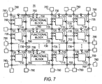
FIG. 7 is a simplified block diagram of a programmable logic device in accordance with the principles of the present invention. -
FIG. 8 illustrates how an aspect of the programmable logic device ofFIG. 7 may be improved in accordance with the principles of the present invention. -
FIG. 9 illustrates another aspect of the programmable logic device ofFIG. 7 may be improved in accordance with the principles of the present invention. -
FIG. 10 is a simplified block diagram of configurable memory cells that selectively drive passgate structures in accordance with the principles of the present invention. -
FIG. 11 is a simplified block diagram of an illustrative system that includes an integrated circuit device that has been improved in accordance with the principles of the present invention. - For the purpose of simplifying the discussion of the principles of the present invention, the techniques and embodiments described herein will focus on NMOS passgates. However, the principles illustrated herein are applicable to similar arrangements involving PMOS passgates.
- As defined herein, a nominal voltage is the voltage that is used predominately throughout an integrated circuit, such as a programmable logic device, and is typically associated with "low" voltages. The nominal voltage is sometimes referred to as a system voltage or a core circuitry voltage.
- As defined herein, a nominal threshold voltage is the threshold voltage of transistors other than the passgate transistors according to the invention that are included in the integrated circuitry (e.g., programmable logic device). A nominal VT may be the VT of a transistor (e.g., a logic transistor) fabricated using a particular process (e.g., a 90nm process) without attempting to produce a VT that would not normally be fabricated according to that particular process.
-
FIG. 1 illustrates one arrangement for reducing leakage current, while maintaining high speed operation of the NMOS passgates in accordance with the principles of the present invention. In the arrangement shown inFIG. 1 , the VT ofNMOS passgate 100 is fabricated to have a higher than nominal VT than other transistors fabricated according to a particular process dimension (e.g., a 90nm process). The voltage being applied to the gate, VGATE, ofNMOS passgate 100 is higher than the nominal voltage. VGATE is sometimes referred to herein as the passgate activation voltage. In some designs, depending on the process being used and the voltage difference between VIN and VGATE or the difference between VOUT and VGATE,NMOS passgate 100 may be a high-voltage tolerant transistor, such as a thick-oxide device, in order to reliably handle voltage being applied to its gate to prevent, for example, gate-oxide breakdown. - For the purposes of the present invention, VGATE may be a static bias voltage or a dynamic signal. In one embodiment, as illustrated in
FIG. 1 , the passgate activation voltage may be derived from any of a variety ofsources 104, such as a dedicated external pin on which a voltage greater than the nominal voltage is provided, an I/O pin (e.g., control/data signals provided from an external source that provides a voltage higher than a nominal voltage), or a positive I/O supply voltage, VDD-I/O (e.g., when the core circuitry and the I/O circuitry have separate power supplies and VDD-I/O is greater than the nominal voltage). - In other embodiments, depending on the application, the passgate activation voltage may also be generated by any of a variety of voltage boosting/conversion circuitry such as charge pumps and voltage converters (e.g., DC/DC, AC/DC, etc.). In yet other embodiments, the passgate activation voltage may be provided by a memory cell such as an SRAM-cell.
- It will be understood that the extent to which the passgate activation voltage exceeds the nominal voltage can vary depending on several factors such as type of transistor and gate-oxide thickness. It will further be understood that the passgate activation voltage exceeds the nominal voltage by a predetermined voltage. For example, the predetermined percentage may range from about one percent to about two hundred percent, depending on various factors.
- The application of this passgate activation voltage to the gates of the passgate structures insures that the desired passgate operation speed is obtained.
- As semiconductor processes continue to decrease in size, VT continues to decrease. As is known in the art, a reduction in VT results in a corresponding increase in leakage current during the "OFF" state. In accordance with the principles of the present invention, it is thus preferable to increase the threshold voltages of those specific transistors being used as passgates.
- One arrangement for accomplishing this is shown in
FIG. 2 , which schematically illustrates a portion of a representativeintegrated circuit device 20, in which two transistors have been fabricated with different threshold voltages. As shown inFIG. 2 ,transistor 200 is configured to operate as something other than a passgate structure and may be fabricated with an associated VT equal to VN (a nominal VT). The other transistor 201 is configured to operate as a passgate, and may be fabricated with an associated VT that is higher than VN by a predetermined percentage. - The above-mentioned predetermined percentage may range from about one percent to about two hundred percent, from about one percent to about one hundred percent, from about one percent to about fifty percent, from about five percent to about forty-five percent, from about ten percent to about forty percent, from about fifteen percent to about thirty-five percent, from about twenty percent to about thirty percent, from about one percent to about thirty percent, from about five percent to about thirty percent, from about ten percent to about thirty percent, from about twenty percent to about forty percent, from about twenty-five percent to about thirty-five percent, or from about thirty percent to about fifty percent.
- It will be understood that any increase in threshold voltage over the nominal threshold voltage assists in minimizing leakage current and is in accordance with the principles of the present invention. Thus it is understood that the present invention is not limited to the percentages enumerated herein.
- Expanding on the arrangement shown in
FIG. 2, FIG. 3 shows a portion of anintegrated circuit device 30, which is divided intodifferent sections 301/302/303, wherein all the transistors within a given section have been fabricated with a specific threshold voltage that may be different from that of the transistors in the other sections. For example,sections sections other sections 303. - As an alternative, or in addition, to selectively fabricating low VT transistors,
FIGS. 4 and 5 illustrate an arrangement wherein a higher than nominal VT may be achieved by controlling the bias voltage, VBIAS, of the well 405 in which theNMOS passgate 400 is fabricated. For the purposes of the present invention,NMOS passgate 400 is preferably fabricated in a well 405 which is capable of being biased to a voltage that is different from that which is used to bias thesubstrate 520. In the illustrative embodiment shown inFIG. 5 , for example, a triple-well process may be used to allow p-well 405 to be biased separately from the p-substrate 520, thereby allowing the VT of NMOS passgate 400 to be adjusted as a function of the source-to-bulk potential difference, VSB, which, in the arrangement shown inFIG. 5 , is dependent on VBIAS. The relationship between VT and VSB for an NMOS transistor, which should be familiar to those skilled in the art, may be expressed as follows:
(wherein Vt0 is the threshold voltage when VSB is zero, g is the body-effect constant, and ΦF is a term associated with the doping of the well). Accordingly, the VT of NMOS passgate 400 may thus be increased by creating a positive VSB by setting the bias voltage, VBIAS, of well 405 to a level that is lower than the voltage level present on the source terminal ofNMOS passgate 400. For the purposes of the present invention, VBIAS should not be too low so as to forward bias the junction between the source/drain 401/402 and the p-well 405. - In accordance with the principles of the present invention, VBIAS may be derived from any of a variety of sources and bias generation schemes 500, which may be either internal or external to the integrated circuit device which includes
NMOS passgate 400. Such sources 500 may include external pins, charge pumps, voltage references, voltage dividers, level-shifters, control/feedback circuitry, and the like. In some designs, VBIAS may be provided as a static voltage, which may or may not correspond to any of the supply voltages used on the integrated circuit device. In other designs, it may be preferable to use a dynamic voltage for VBIAS, which may be provided by a control circuit that generates a variable VBIAS that may be a function of any of a variety of parameters, such as process variations, temperature, voltage, current, or a combination thereof. As a result, the VT of NMOS passgate 400 may be tuned in a feedback loop to achieve a high VT that, when coupled with higher than nominal gate voltages, optimizes, for example, the tradeoff between high speed passgate operation and reducing leakage current. -
FIGS. 6A and6B show graphs comparing performance characteristics of passgate structures constructed according to the invention and to other transistors not being used as passgates, both of which are fabricated according to a given process dimension. BothFIGS. 6A and6B show an illustrative trend in supply voltages (line 610) for a given process dimension.FIGS. 6A and6B show an illustrative trend of nominal threshold voltages, VTN, of transistors other than the passgate structures according to the invention.FIGS. 6A and6B also illustratively show a higher than nominal threshold voltages, VTN+, of the passgate structures according to the invention. Note that the supply voltage decreases as the process dimension decreases. Further note that VTN decreases as the process dimension decreases, whereas VTN+ is higher than VTN by a predetermined percentage for various process dimensions (e.g., process dimensions smaller than 0.13µm). Yet further note that a portion of the trends shown inFIGS. 6A and6B have dashed lines. These dashed lines generally represent anticipated values of voltage, leakage current, and frequency that may be obtained in future process dimensions. - Referring now specifically to
FIG. 6A , the leakage current (line 612) for a transistor having VTN is compared to the leakage current (line 614) for a passgate transistor having VTN+ for a given process. Note that for "larger" processes (e.g., greater than 0.13µm processes), the threshold voltage of the passgate structures need not be higher than the nominal threshold voltage. Thus, this is whyFIGS. 6A and6B do not show the VTN+ "circles" extending to the far left in the figure. As shown, the leakage current is low for transistors fabricated according to "larger" process dimensions and that have a threshold voltage of VTN. However, as the process dimension decreases, the leakage current for transistors having VTN rises dramatically, whereas the leakage current for transistors having VTN+ remains relatively low (i.e., the leakage current is reduced compared to the leakage current experienced by transistors having a nominal threshold voltage). - Referring now to
FIG. 6B , the frequency of transistors having VTN or VTN+ and being driven by a nominal voltage or passgate activation voltage are compared.Line 620 represents an "ideal" operational speed attained with transistors having VTN and being driven by a nominal voltage. However, this speed is achieved at the cost of high leakage current, as indicated byline 612 inFIG. 6A .Line 630 represents a speed profile of transistors having VTN+, but is driven with a nominal gate voltage. As shown inFIG. 6B , the speed ofline 630 is substantially less than ideal at the smaller process dimensions. However, line 640, which represents the speed of passgate transistors according to the invention have VTN+ and are driven by a passgate activation voltage (e.g., a voltage higher than the nominal voltage), substantially matches the ideal speed ofline 620, while at the same time benefits from having a relative low leakage current. - The above-described
passgate structures 10/201/40 that may be constructed in accordance with the principles of the present invention are especially useful in integrated circuit devices, such as programmable logic devices, in which such passgate structures are used as interconnection switches to allow programmable routing and switching.FIG. 7 is a simplified block diagram of an illustrativeprogrammable logic device 70 in which interconnection switches using passgate structures that have been constructed in accordance with the principles of the present invention may be readily used.Programmable logic device 70 includes a plurality of regions ofprogrammable logic 710 operatively disposed in a two-dimensional array of rows and columns, and a programmable network of horizontal 730 and vertical 735 interconnection conductors for conveying signals amongst thelogic regions 710 and various I/O structures 780. In the network ofinterconnection conductors 730/735, signals may be programmably routed via interconnection switches 700, which, in some designs, may also be grouped to form multiplexers. In some embodiments,programmable logic device 70 may also include any of a variety offunctional blocks 750, such as memory structures, multiplier/accumulator blocks, arithmetic logic units, microprocessors, etc.Functional blocks 750 may be dedicated structures that are configured to implement a specific function, or, alternatively, they may be user-programmable/reconfigurable structures. -
FIG. 8 illustrates in greater detail how interconnection switches 700 may be used in the network ofinterconnection conductors 730/735 to route signals withinprogrammable logic device 70. For the purpose of illustrating the principles of the present invention, a signal source/destination withinprogrammable logic device 70 may be any of thelogic regions 710,functional blocks 750, I/O structures 780, or other circuitry withinprogrammable logic device 70. As schematically illustrated inFIG. 8 , a signal may be routed from any given source to any given destination by usinginterconnection switches 700 to multiplex or switch signals provided on the output leads 725 ofsignal source 710/750/780/etc. onto the network ofinterconnection conductors 730/735 (within which interconnection switches 700 may also be used to programmably connect one interconnection conductor to another), from which the signal may be eventually multiplexed or switched onto theinput lead 720 ofsignal destination 710/750/780/etc. As shown inFIG. 8 , the electrical characteristics of the network ofinterconnection conductors 730/735 may be represented as a chain ofresistors 820 andcapacitors 821a/b in a "black-box" abstraction. - Also shown in
FIG. 8 is one embodiment of aninterconnection switch 700 that may be constructed using the above-described enhanced passgate structures in accordance with the principles of the present invention. As illustrated inFIG. 8 ,interconnection switch 700 may include any of thepassgates 10/201/40 as the switching mechanism. In some embodiments, a pair ofinverters PMOS transistor 802, may also be included to provide buffering of the input and output signals. Half-latch PMOS transistor 802 may be used to recover from the voltage drop across thepassgate 10/201/40. -
FIG. 9 shows another embodiment of aninterconnection switch 900 that may be constructed using the above-described enhanced passgate structures in accordance with the principles of the present invention. As illustrated inFIG. 9 ,interconnection switch 900 may include two ofpassgates 10/201/40 for use as a dual-passgate switching mechanism. If desired, switch 900 may includeinverters interconnection switch 900 can be used in place or intermixed withinterconnection switch 700 inFIG. 7 . -
FIG. 10 shows a portion of anintegrated circuit 1000 employing the use ofmemory cells 1010 to drivepassgate transistors 700/900 according to the principles of the present invention.Memory cells 1010 may be configurable ram cells such as SRAM cells.Passgate transistors 700/900 may be any of the enhanced passgate structures that have been described in the foregoing. - Also shown in
FIG. 10 is a higher than nominal voltage source, Vccx, which is coupled tomemory cells 1010. As discussed above, the higher than nominal voltage may be supplied by a separate I/O pin that provides a supply voltage higher than the nominal supply voltage, generated from a charge pump, a voltage leveler, or the like. - An advantage realized by powering
memory cells 1010 with a higher than nominal voltage is that it reduces the potential for soft-error. Soft-error occurs when the logic state being stored in the memory cell inadvertently changes. Soft-error can be caused by, for example, sub-atomic particles (sometimes referred to as alpha particles or neutron beams) that disrupt the operation of silicon by changing the charge of the memory cell. Soft-error can also be caused by cross-coupling of memory cells. As supply voltages (e.g., nominal voltages) continue to decrease, the soft-error-rate increases because the critical charge needed to flip the cell decreases as the supply voltage decreases. Therefore, application of Vccx, as opposed to a nominal voltage, provides a supply voltage that enablesmemory cells 1010 to operate with a relatively low soft-error-rate. - Thus, a synergy is created among
memory cells 1010 and thepassgate transistors 700/900 because Vccx provides voltage sufficient to minimize soft-error and is also sufficient to drive passgate transistors at a predetermined operational speed (i.e., Vccx is at least equal to the passgate activation voltage). That is,memory cells 1010 selectively drivepassgate transistors 700/900 by applying the voltage provided by Vccx (e.g., a passgate activation voltage) to the gates of thepassgate transistors 700/900. Thus, the advantage of poweringmemory cells 1010 with higher than nominal voltage prevents inadvertent flipping, while at the same time enablesmemory cells 1010 to drive passgates 700/900 with the requisite voltage. -
FIG. 11 shows how an integrated circuit device 1190 (e.g., a programmable logic device) employing any of the enhanced passgate structures that have been described in the foregoing may be used in asystem 1100.System 1100 may include one or more of the following components: variousperipheral devices 1102, I/O circuitry 1103, aprocessor 1104, and amemory 1105. These components may be coupled together by asystem bus 1101 and may be populated on acircuit board 1106 which is contained in an end-user system 1107. -
System 1100 can be used in a wide variety of applications, such as computer networking, data networking, instrumentation, video processing, digital signal processing, or any other application where the advantage of using programmable or reprogrammable logic is desirable. Integrated circuit device 90, employing passgate structures that have been constructed in accordance with the principles of the present invention, may be used to perform a variety of different logic functions. For example, integratedcircuit device 1190 can be configured as a processor or controller that works in cooperation withprocessor 1104.Integrated circuit device 1190 may also be used as an arbiter for arbitrating access to a shared resource insystem 1100. In yet another example, integratedcircuit device 1190 may be configured as an interface betweenprocessor 1104 and one of the other components in system - Various technologies may be used to implement the
integrated circuit device 1190 employing passgate structures that have been constructed in accordance with the principles of the present invention. Moreover, this invention is applicable to both one-time-only programmable and reprogrammable devices. - Thus, it is seen that enhanced passgate structures for an integrated circuit device have been presented. One skilled in the art will appreciate that the present invention may be practiced by other than the described embodiments, which are presented for purposes of illustration and not of limitation, and the present invention is limited only by the claims which follow.
Claims (22)
- An integrated circuit (1190), comprising:a first set of transistors (200) having a nominal threshold voltage, wherein each transistor of said first set can be selectively activated by applying a nominal voltage to its gate terminal; anda set of passgate transistors (201, 700, 900) have a passgate threshold voltage that is higher than the nominal threshold voltage of the transistors of said first set by a predetermined percentage, wherein each passgate transistor (201, 700, 900) can be selectively activated by applying a passgate activation voltage that exceeds the nominal voltage to the gate terminal of each passgate transistor, andat least one memory cell (1010) that is powered with a memory cell supply voltage that is equal to or greater than the passgate activation voltage, wherein said at least one memory cell is coupled to at least one of the pass gate transistors and is operative to selectively provide the passgate activation voltage to a gate terminal of at least one passgate transistor (201, 700, 900).
- The integrated circuit defined in claim 1, wherein said predetermined percentage ranges from one percent to two hundred percent.
- The integrated circuit defined in claim 1, wherein said predetermined percentage ranges from five percent to forty percent.
- The integrated circuit defined in claim 1, wherein said predetermined percentage ranges from ten percent to thirty-five percent.
- 5. The integrated circuit defined in claim 1, wherein said predetermined percentage ranges from fifteen percent to thirty percent.
- The integrated circuit defined in claim 1, wherein said nominal voltage is a supply voltage provided to the integrated circuit (1190).
- The integrated circuit defined in claim 1, further comprising a passgate activation voltage source that provides the passgate activation voltage.
- The integrated circuit defined in claim 7, wherein the passgate activation voltage source is provided by a level-shifter, a charge pump, a reference voltage generator, a voltage divider circuit, or an input/output pin on the integrated circuit.
- The integrated circuit defined in claim 1, wherein the memory cell (1010) is an SRAM cell.
- The integrated circuit defined in claim 1, wherein said passgate transistors (201, 700, 900) are NMOS transistors.
- The integrated circuit defined in claim 1 further comprising:an array of logic blocks (710);a plurality of interconnect lines (730, 735); anda plurality of switches (700) for programmably routing logic signals between the logic blocks over the interconnect lines, wherein each switch includes at least one of the passgate transistors.
- A digital processing system comprising:processing circuitry;a system memory coupled to the processing circuitry; andthe integrated circuit defined in claim 1 coupled to the processing circuitry and the system memory.
- A printed circuit board on which is mounted the integrated circuit defined in claim 1.
- The printed circuit board defined in claim 13 further comprising:a board memory mounted on the printed circuit board and coupled to the integrated circuit device.
- The printed circuit board defined in claim 14 further comprising:processing circuitry mounted on the printed circuit board and coupled to the integrated circuit device.
- The integrated circuit defined in claim 10 further comprising a plurality of memory cells that are powered with a memory cell supply voltage that is equal to or greater than the passgate activation voltage.
- The integrated circuit defined in claim 16, wherein the memory cells selectively provide the passgate activation voltage to the passgate transistors.
- The integrated circuit defined in claim 16, wherein the memory cells are SRAM cells.
- The integrated circuit defined in claim 16, wherein the memory cell supply voltage is provided by a level-shifter, a charge pump, a reference voltage generator, a voltage divider circuit, or an input/output pin on the programmable logic device.
- The integrated circuit defined in claim 10, wherein at least one of the passgate transistors is fabricated to have said threshold voltage that is higher than the threshold voltage of the other transistors.
- The integrated circuit defined in claim 10, wherein at least one of the passgate transistors is a semiconductor transistor comprising a gate well region and a connection for biasing the gate well region with respect to other regions of the semiconductor transistor, thereby setting a threshold voltage of the passgate transistor to a voltage level higher than the nominal threshold voltage.
- The integrated circuit defined in claim 10, wherein the passgate transistors are NMOS transistors.
Applications Claiming Priority (2)
| Application Number | Priority Date | Filing Date | Title |
|---|---|---|---|
| US10/910,891 US7292065B2 (en) | 2004-08-03 | 2004-08-03 | Enhanced passgate structures for reducing leakage current |
| PCT/US2005/027416 WO2006017501A1 (en) | 2004-08-03 | 2005-08-02 | Enhanced passgate structures for reducing leakage current |
Publications (2)
| Publication Number | Publication Date |
|---|---|
| EP1779513A1 EP1779513A1 (en) | 2007-05-02 |
| EP1779513B1 true EP1779513B1 (en) | 2012-03-14 |
Family
ID=35756807
Family Applications (1)
| Application Number | Title | Priority Date | Filing Date |
|---|---|---|---|
| EP05778119A Expired - Lifetime EP1779513B1 (en) | 2004-08-03 | 2005-08-02 | Enhanced passgate structures for reducing leakage current |
Country Status (6)
| Country | Link |
|---|---|
| US (1) | US7292065B2 (en) |
| EP (1) | EP1779513B1 (en) |
| JP (1) | JP2008509604A (en) |
| CN (1) | CN101027838B (en) |
| AT (1) | ATE549797T1 (en) |
| WO (1) | WO2006017501A1 (en) |
Families Citing this family (12)
| Publication number | Priority date | Publication date | Assignee | Title |
|---|---|---|---|---|
| US5457410A (en) * | 1993-08-03 | 1995-10-10 | Btr, Inc. | Architecture and interconnect scheme for programmable logic circuits |
| JP4635188B2 (en) * | 2006-07-25 | 2011-02-16 | 独立行政法人産業技術総合研究所 | MOS circuit with four-terminal double insulated gate field transistor |
| US7673202B2 (en) * | 2006-09-28 | 2010-03-02 | Cisco Technology, Inc. | Single event upset test circuit and methodology |
| US7893723B2 (en) * | 2007-12-29 | 2011-02-22 | Texas Instruments Incorporated | Minimizing leakage in logic designs |
| JP5414061B2 (en) * | 2010-03-24 | 2014-02-12 | 独立行政法人産業技術総合研究所 | Logic circuit, selector circuit and integrated circuit using pass transistor |
| US8581625B2 (en) * | 2011-05-19 | 2013-11-12 | Semiconductor Energy Laboratory Co., Ltd. | Programmable logic device |
| US8804407B1 (en) | 2011-07-12 | 2014-08-12 | Altera Corporation | PMOS pass gate |
| US8723592B2 (en) * | 2011-08-12 | 2014-05-13 | Nxp B.V. | Adjustable body bias circuit |
| US8705605B1 (en) | 2011-11-03 | 2014-04-22 | Altera Corporation | Technique for providing loopback testing with single stage equalizer |
| US8995175B1 (en) * | 2012-01-13 | 2015-03-31 | Altera Corporation | Memory circuit with PMOS access transistors |
| US9628081B2 (en) * | 2014-08-12 | 2017-04-18 | Xilinx, Inc. | Interconnect circuits having low threshold voltage P-channel transistors for a programmable integrated circuit |
| CN112951830B (en) * | 2021-02-01 | 2023-02-07 | 泉芯集成电路制造(济南)有限公司 | Integrated Circuit Devices, Memory and Electronic Devices |
Family Cites Families (41)
| Publication number | Priority date | Publication date | Assignee | Title |
|---|---|---|---|---|
| USRE34363E (en) | 1984-03-12 | 1993-08-31 | Xilinx, Inc. | Configurable electrical circuit having configurable logic elements and configurable interconnects |
| US4713557A (en) | 1984-09-26 | 1987-12-15 | Xilinx, Inc. | Bidirectional buffer amplifier |
| US4821233A (en) | 1985-09-19 | 1989-04-11 | Xilinx, Incorporated | 5-transistor memory cell with known state on power-up |
| US4831596A (en) | 1987-05-01 | 1989-05-16 | Texas Instruments Incorporated | Pass gate with low transistor junction breakdown susceptibility |
| JPH07105160B2 (en) | 1989-05-20 | 1995-11-13 | 東芝マイクロエレクトロニクス株式会社 | Semiconductor memory device |
| EP0615668A4 (en) | 1991-10-30 | 1995-03-01 | Xilinx Inc | Regulator for pumped voltage generator. |
| US5291079A (en) | 1992-07-23 | 1994-03-01 | Xilinx, Inc. | Configuration control unit for programming a field programmable gate array and reading array status |
| US5455582A (en) * | 1992-12-17 | 1995-10-03 | Ulsi Technology, Inc. | Digital to analog converter employing R-2R ladders with substituted shunt arms |
| JP3189464B2 (en) * | 1993-02-19 | 2001-07-16 | 株式会社デンソー | Rotational position detector |
| JP3494469B2 (en) * | 1994-05-26 | 2004-02-09 | 株式会社ルネサステクノロジ | Field programmable gate array |
| US5544097A (en) * | 1995-03-31 | 1996-08-06 | Sgs-Thomson Microelectronics, Inc. | SRAM memory cell with reduced internal cell voltage |
| DE19524658C1 (en) | 1995-07-06 | 1996-10-24 | Siemens Ag | Bootstrap circuit using transfer transistor |
| US5717340A (en) | 1996-01-17 | 1998-02-10 | Xilink, Inc. | Circuit for testing pumped voltage gates in a programmable gate array |
| US5959933A (en) * | 1996-01-25 | 1999-09-28 | Micron Technology, Inc. | System for improved memory cell access |
| US6005806A (en) | 1996-03-14 | 1999-12-21 | Altera Corporation | Nonvolatile configuration cells and cell arrays |
| JPH09293789A (en) * | 1996-04-24 | 1997-11-11 | Mitsubishi Electric Corp | Semiconductor integrated circuit |
| US5821771A (en) * | 1996-05-21 | 1998-10-13 | Altera Corporation | Method and apparatus for monitoring or forcing an internal node in a programmable device |
| US5760605A (en) * | 1996-09-30 | 1998-06-02 | Advanced Micro Devices, Inc. | Programmable high speed routing switch |
| US5706226A (en) | 1996-12-31 | 1998-01-06 | Sgs-Thomson Microelectronics, Inc. | Low voltage CMOS SRAM |
| US6097238A (en) | 1997-01-10 | 2000-08-01 | Xilinx, Inc. | Circuit with ramp-up control and overcoming a threshold voltage loss in an NMOS transistor |
| US5877612A (en) * | 1997-03-24 | 1999-03-02 | The United States Of America As Represented By The Secretary Of The Navy | Amplification of signals from high impedance sources |
| US5880620A (en) | 1997-04-22 | 1999-03-09 | Xilinx, Inc. | Pass gate circuit with body bias control |
| US6535034B1 (en) | 1997-07-30 | 2003-03-18 | Programmable Silicon Solutions | High performance integrated circuit devices adaptable to use lower supply voltages with smaller device geometries |
| US5841694A (en) | 1997-07-30 | 1998-11-24 | Programmable Silicon Solutions | High performance programmable interconnect |
| JP3114680B2 (en) * | 1997-12-15 | 2000-12-04 | 日本電気株式会社 | Active filter |
| US6583662B1 (en) * | 1999-06-23 | 2003-06-24 | Globespanvirata, Inc. | Circuit and method for implementing an integrated continuous-time smoothing filter |
| US6278290B1 (en) | 1999-08-13 | 2001-08-21 | Xilinx, Inc. | Method and circuit for operating programmable logic devices during power-up and stand-by modes |
| US6396325B2 (en) | 1999-12-03 | 2002-05-28 | Fairchild Semiconductor Corporation | High frequency MOSFET switch |
| US6504212B1 (en) * | 2000-02-03 | 2003-01-07 | International Business Machines Corporation | Method and apparatus for enhanced SOI passgate operations |
| US6563367B1 (en) * | 2000-08-16 | 2003-05-13 | Altera Corporation | Interconnection switch structures |
| US6661253B1 (en) * | 2000-08-16 | 2003-12-09 | Altera Corporation | Passgate structures for use in low-voltage applications |
| US6577514B2 (en) * | 2001-04-05 | 2003-06-10 | Saifun Semiconductors Ltd. | Charge pump with constant boosted output voltage |
| MXPA01007171A (en) * | 2001-07-13 | 2003-01-27 | Hector Mendoza Orozco | Improved safety catch for an ammunitions sportive rifle. |
| CN1399407A (en) * | 2001-07-26 | 2003-02-26 | 中国科学院微电子中心 | Bootstrap-complementary transmission gate charge-restoring low-power consumption circuit structure |
| US6621325B2 (en) | 2001-09-18 | 2003-09-16 | Xilinx, Inc. | Structures and methods for selectively applying a well bias to portions of a programmable device |
| EP1438662A2 (en) | 2001-10-11 | 2004-07-21 | Altera Corporation | Error detection on programmable logic resources |
| JP3522248B2 (en) | 2001-10-15 | 2004-04-26 | ローム株式会社 | Semiconductor integrated circuit device |
| US6492876B1 (en) * | 2001-10-25 | 2002-12-10 | National Semiconductor Corporation | Low power analog equalizer with variable op-amp gain |
| US6930510B2 (en) | 2003-03-03 | 2005-08-16 | Xilinx, Inc. | FPGA architecture with mixed interconnect resources optimized for fast and low-power routing and methods of utilizing the same |
| US6876572B2 (en) | 2003-05-21 | 2005-04-05 | Altera Corporation | Programmable logic devices with stabilized configuration cells for reduced soft error rates |
| WO2005013490A1 (en) | 2003-08-05 | 2005-02-10 | Koninklijke Philips Electronics N.V. | Switch module for a field programmable logic circuit |
-
2004
- 2004-08-03 US US10/910,891 patent/US7292065B2/en not_active Expired - Fee Related
-
2005
- 2005-08-02 CN CN2005800263612A patent/CN101027838B/en not_active Expired - Fee Related
- 2005-08-02 JP JP2007524911A patent/JP2008509604A/en not_active Withdrawn
- 2005-08-02 EP EP05778119A patent/EP1779513B1/en not_active Expired - Lifetime
- 2005-08-02 AT AT05778119T patent/ATE549797T1/en active
- 2005-08-02 WO PCT/US2005/027416 patent/WO2006017501A1/en not_active Ceased
Also Published As
| Publication number | Publication date |
|---|---|
| CN101027838B (en) | 2010-10-27 |
| US20060028240A1 (en) | 2006-02-09 |
| CN101027838A (en) | 2007-08-29 |
| JP2008509604A (en) | 2008-03-27 |
| ATE549797T1 (en) | 2012-03-15 |
| US7292065B2 (en) | 2007-11-06 |
| EP1779513A1 (en) | 2007-05-02 |
| WO2006017501A1 (en) | 2006-02-16 |
Similar Documents
| Publication | Publication Date | Title |
|---|---|---|
| US7800405B2 (en) | Passgate structures for use in low-voltage applications | |
| EP1304803B1 (en) | Programmable logic device comprising silicon-on-insulator transistors | |
| JP4149011B2 (en) | Method of assembling integrated circuit, integrated circuit, and high voltage tolerant interface circuit for integrated circuit | |
| US6940307B1 (en) | Integrated circuits with reduced standby power consumption | |
| EP0305676A2 (en) | CMOS off-chip driver circuit | |
| US6262599B1 (en) | Level shifting CMOS I/O buffer | |
| CN101174828B (en) | Programmable multiple supply regions with switched pass gate level converters | |
| KR20000071306A (en) | Overvoltage/undervoltage tolerant transfer gate | |
| US20060273825A1 (en) | Level conversion circuit and semiconductor integrated circuit device employing the level conversion circuit | |
| KR20000070951A (en) | High-voltage cmos level shifter | |
| KR20030006958A (en) | Semiconductor integrated circuit, the semiconductor designing method and the program for designing the same | |
| US7292065B2 (en) | Enhanced passgate structures for reducing leakage current | |
| US12407350B2 (en) | Voltage level shifter with programmable high supply voltage and high supply voltage-dependent variable low supply voltage | |
| JPH08148986A (en) | Output buffer circuit | |
| US6998668B2 (en) | Semiconductor integrated circuit device including a level shifter | |
| WO2005048454A2 (en) | Multiplexer circuits | |
| US6064223A (en) | Low leakage circuit configuration for MOSFET circuits | |
| US7639042B2 (en) | Methods of reducing power in programmable logic devices using low voltage swing for routing signals | |
| US6028444A (en) | Three-statable net driver for antifuse field programmable gate array | |
| US6414518B1 (en) | Circuitry for a low internal voltage integrated circuit | |
| GB2334391A (en) | CMOS standby current reduction | |
| WO2005013490A1 (en) | Switch module for a field programmable logic circuit |
Legal Events
| Date | Code | Title | Description |
|---|---|---|---|
| PUAI | Public reference made under article 153(3) epc to a published international application that has entered the european phase |
Free format text: ORIGINAL CODE: 0009012 |
|
| 17P | Request for examination filed |
Effective date: 20070208 |
|
| AK | Designated contracting states |
Kind code of ref document: A1 Designated state(s): AT BE BG CH CY CZ DE DK EE ES FI FR GB GR HU IE IS IT LI LT LU LV MC NL PL PT RO SE SI SK TR |
|
| RIN1 | Information on inventor provided before grant (corrected) |
Inventor name: HOANG, TIM TRI Inventor name: LUI, HENRY Y. Inventor name: KABANI, MALIK Inventor name: PATEL, RAKESH |
|
| DAX | Request for extension of the european patent (deleted) | ||
| 17Q | First examination report despatched |
Effective date: 20100202 |
|
| REG | Reference to a national code |
Ref country code: DE Ref legal event code: R079 Ref document number: 602005033174 Country of ref document: DE Free format text: PREVIOUS MAIN CLASS: H03K0019000000 Ipc: H03K0019177000 |
|
| GRAP | Despatch of communication of intention to grant a patent |
Free format text: ORIGINAL CODE: EPIDOSNIGR1 |
|
| RIC1 | Information provided on ipc code assigned before grant |
Ipc: H03K 19/177 20060101AFI20111006BHEP |
|
| GRAS | Grant fee paid |
Free format text: ORIGINAL CODE: EPIDOSNIGR3 |
|
| GRAA | (expected) grant |
Free format text: ORIGINAL CODE: 0009210 |
|
| AK | Designated contracting states |
Kind code of ref document: B1 Designated state(s): AT BE BG CH CY CZ DE DK EE ES FI FR GB GR HU IE IS IT LI LT LU LV MC NL PL PT RO SE SI SK TR |
|
| REG | Reference to a national code |
Ref country code: GB Ref legal event code: FG4D |
|
| REG | Reference to a national code |
Ref country code: CH Ref legal event code: EP Ref country code: AT Ref legal event code: REF Ref document number: 549797 Country of ref document: AT Kind code of ref document: T Effective date: 20120315 |
|
| REG | Reference to a national code |
Ref country code: IE Ref legal event code: FG4D |
|
| REG | Reference to a national code |
Ref country code: DE Ref legal event code: R096 Ref document number: 602005033174 Country of ref document: DE Effective date: 20120510 |
|
| REG | Reference to a national code |
Ref country code: NL Ref legal event code: T3 |
|
| PG25 | Lapsed in a contracting state [announced via postgrant information from national office to epo] |
Ref country code: LT Free format text: LAPSE BECAUSE OF FAILURE TO SUBMIT A TRANSLATION OF THE DESCRIPTION OR TO PAY THE FEE WITHIN THE PRESCRIBED TIME-LIMIT Effective date: 20120314 |
|
| LTIE | Lt: invalidation of european patent or patent extension |
Effective date: 20120314 |
|
| PG25 | Lapsed in a contracting state [announced via postgrant information from national office to epo] |
Ref country code: GR Free format text: LAPSE BECAUSE OF FAILURE TO SUBMIT A TRANSLATION OF THE DESCRIPTION OR TO PAY THE FEE WITHIN THE PRESCRIBED TIME-LIMIT Effective date: 20120615 Ref country code: LV Free format text: LAPSE BECAUSE OF FAILURE TO SUBMIT A TRANSLATION OF THE DESCRIPTION OR TO PAY THE FEE WITHIN THE PRESCRIBED TIME-LIMIT Effective date: 20120314 Ref country code: FI Free format text: LAPSE BECAUSE OF FAILURE TO SUBMIT A TRANSLATION OF THE DESCRIPTION OR TO PAY THE FEE WITHIN THE PRESCRIBED TIME-LIMIT Effective date: 20120314 |
|
| REG | Reference to a national code |
Ref country code: AT Ref legal event code: MK05 Ref document number: 549797 Country of ref document: AT Kind code of ref document: T Effective date: 20120314 |
|
| PG25 | Lapsed in a contracting state [announced via postgrant information from national office to epo] |
Ref country code: CY Free format text: LAPSE BECAUSE OF FAILURE TO SUBMIT A TRANSLATION OF THE DESCRIPTION OR TO PAY THE FEE WITHIN THE PRESCRIBED TIME-LIMIT Effective date: 20120314 |
|
| PG25 | Lapsed in a contracting state [announced via postgrant information from national office to epo] |
Ref country code: RO Free format text: LAPSE BECAUSE OF FAILURE TO SUBMIT A TRANSLATION OF THE DESCRIPTION OR TO PAY THE FEE WITHIN THE PRESCRIBED TIME-LIMIT Effective date: 20120314 Ref country code: IS Free format text: LAPSE BECAUSE OF FAILURE TO SUBMIT A TRANSLATION OF THE DESCRIPTION OR TO PAY THE FEE WITHIN THE PRESCRIBED TIME-LIMIT Effective date: 20120714 Ref country code: SI Free format text: LAPSE BECAUSE OF FAILURE TO SUBMIT A TRANSLATION OF THE DESCRIPTION OR TO PAY THE FEE WITHIN THE PRESCRIBED TIME-LIMIT Effective date: 20120314 Ref country code: BE Free format text: LAPSE BECAUSE OF FAILURE TO SUBMIT A TRANSLATION OF THE DESCRIPTION OR TO PAY THE FEE WITHIN THE PRESCRIBED TIME-LIMIT Effective date: 20120314 Ref country code: CZ Free format text: LAPSE BECAUSE OF FAILURE TO SUBMIT A TRANSLATION OF THE DESCRIPTION OR TO PAY THE FEE WITHIN THE PRESCRIBED TIME-LIMIT Effective date: 20120314 Ref country code: SE Free format text: LAPSE BECAUSE OF FAILURE TO SUBMIT A TRANSLATION OF THE DESCRIPTION OR TO PAY THE FEE WITHIN THE PRESCRIBED TIME-LIMIT Effective date: 20120314 Ref country code: EE Free format text: LAPSE BECAUSE OF FAILURE TO SUBMIT A TRANSLATION OF THE DESCRIPTION OR TO PAY THE FEE WITHIN THE PRESCRIBED TIME-LIMIT Effective date: 20120314 Ref country code: PL Free format text: LAPSE BECAUSE OF FAILURE TO SUBMIT A TRANSLATION OF THE DESCRIPTION OR TO PAY THE FEE WITHIN THE PRESCRIBED TIME-LIMIT Effective date: 20120314 |
|
| PG25 | Lapsed in a contracting state [announced via postgrant information from national office to epo] |
Ref country code: SK Free format text: LAPSE BECAUSE OF FAILURE TO SUBMIT A TRANSLATION OF THE DESCRIPTION OR TO PAY THE FEE WITHIN THE PRESCRIBED TIME-LIMIT Effective date: 20120314 Ref country code: PT Free format text: LAPSE BECAUSE OF FAILURE TO SUBMIT A TRANSLATION OF THE DESCRIPTION OR TO PAY THE FEE WITHIN THE PRESCRIBED TIME-LIMIT Effective date: 20120716 |
|
| PLBE | No opposition filed within time limit |
Free format text: ORIGINAL CODE: 0009261 |
|
| STAA | Information on the status of an ep patent application or granted ep patent |
Free format text: STATUS: NO OPPOSITION FILED WITHIN TIME LIMIT |
|
| PG25 | Lapsed in a contracting state [announced via postgrant information from national office to epo] |
Ref country code: AT Free format text: LAPSE BECAUSE OF FAILURE TO SUBMIT A TRANSLATION OF THE DESCRIPTION OR TO PAY THE FEE WITHIN THE PRESCRIBED TIME-LIMIT Effective date: 20120314 Ref country code: DK Free format text: LAPSE BECAUSE OF FAILURE TO SUBMIT A TRANSLATION OF THE DESCRIPTION OR TO PAY THE FEE WITHIN THE PRESCRIBED TIME-LIMIT Effective date: 20120314 |
|
| 26N | No opposition filed |
Effective date: 20121217 |
|
| PG25 | Lapsed in a contracting state [announced via postgrant information from national office to epo] |
Ref country code: IT Free format text: LAPSE BECAUSE OF FAILURE TO SUBMIT A TRANSLATION OF THE DESCRIPTION OR TO PAY THE FEE WITHIN THE PRESCRIBED TIME-LIMIT Effective date: 20120314 |
|
| REG | Reference to a national code |
Ref country code: CH Ref legal event code: PL |
|
| PG25 | Lapsed in a contracting state [announced via postgrant information from national office to epo] |
Ref country code: MC Free format text: LAPSE BECAUSE OF NON-PAYMENT OF DUE FEES Effective date: 20120831 |
|
| REG | Reference to a national code |
Ref country code: DE Ref legal event code: R097 Ref document number: 602005033174 Country of ref document: DE Effective date: 20121217 |
|
| GBPC | Gb: european patent ceased through non-payment of renewal fee |
Effective date: 20120802 |
|
| PG25 | Lapsed in a contracting state [announced via postgrant information from national office to epo] |
Ref country code: LI Free format text: LAPSE BECAUSE OF NON-PAYMENT OF DUE FEES Effective date: 20120831 Ref country code: ES Free format text: LAPSE BECAUSE OF FAILURE TO SUBMIT A TRANSLATION OF THE DESCRIPTION OR TO PAY THE FEE WITHIN THE PRESCRIBED TIME-LIMIT Effective date: 20120625 Ref country code: CH Free format text: LAPSE BECAUSE OF NON-PAYMENT OF DUE FEES Effective date: 20120831 |
|
| REG | Reference to a national code |
Ref country code: IE Ref legal event code: MM4A |
|
| PG25 | Lapsed in a contracting state [announced via postgrant information from national office to epo] |
Ref country code: IE Free format text: LAPSE BECAUSE OF NON-PAYMENT OF DUE FEES Effective date: 20120802 Ref country code: BG Free format text: LAPSE BECAUSE OF FAILURE TO SUBMIT A TRANSLATION OF THE DESCRIPTION OR TO PAY THE FEE WITHIN THE PRESCRIBED TIME-LIMIT Effective date: 20120614 Ref country code: GB Free format text: LAPSE BECAUSE OF NON-PAYMENT OF DUE FEES Effective date: 20120802 |
|
| PG25 | Lapsed in a contracting state [announced via postgrant information from national office to epo] |
Ref country code: TR Free format text: LAPSE BECAUSE OF FAILURE TO SUBMIT A TRANSLATION OF THE DESCRIPTION OR TO PAY THE FEE WITHIN THE PRESCRIBED TIME-LIMIT Effective date: 20120314 |
|
| PG25 | Lapsed in a contracting state [announced via postgrant information from national office to epo] |
Ref country code: LU Free format text: LAPSE BECAUSE OF NON-PAYMENT OF DUE FEES Effective date: 20120802 |
|
| PG25 | Lapsed in a contracting state [announced via postgrant information from national office to epo] |
Ref country code: HU Free format text: LAPSE BECAUSE OF FAILURE TO SUBMIT A TRANSLATION OF THE DESCRIPTION OR TO PAY THE FEE WITHIN THE PRESCRIBED TIME-LIMIT Effective date: 20050802 |
|
| REG | Reference to a national code |
Ref country code: FR Ref legal event code: PLFP Year of fee payment: 12 |
|
| PGFP | Annual fee paid to national office [announced via postgrant information from national office to epo] |
Ref country code: NL Payment date: 20160805 Year of fee payment: 12 |
|
| PGFP | Annual fee paid to national office [announced via postgrant information from national office to epo] |
Ref country code: FR Payment date: 20160719 Year of fee payment: 12 |
|
| REG | Reference to a national code |
Ref country code: NL Ref legal event code: MM Effective date: 20170901 |
|
| REG | Reference to a national code |
Ref country code: FR Ref legal event code: ST Effective date: 20180430 |
|
| PG25 | Lapsed in a contracting state [announced via postgrant information from national office to epo] |
Ref country code: NL Free format text: LAPSE BECAUSE OF NON-PAYMENT OF DUE FEES Effective date: 20170901 |
|
| PG25 | Lapsed in a contracting state [announced via postgrant information from national office to epo] |
Ref country code: FR Free format text: LAPSE BECAUSE OF NON-PAYMENT OF DUE FEES Effective date: 20170831 |
|
| PGFP | Annual fee paid to national office [announced via postgrant information from national office to epo] |
Ref country code: DE Payment date: 20180717 Year of fee payment: 14 |
|
| REG | Reference to a national code |
Ref country code: DE Ref legal event code: R119 Ref document number: 602005033174 Country of ref document: DE |
|
| PG25 | Lapsed in a contracting state [announced via postgrant information from national office to epo] |
Ref country code: DE Free format text: LAPSE BECAUSE OF NON-PAYMENT OF DUE FEES Effective date: 20200303 |