EP1777780A2 - Enhanced bandwidth single layer current sheet antenna - Google Patents
Enhanced bandwidth single layer current sheet antenna Download PDFInfo
- Publication number
- EP1777780A2 EP1777780A2 EP06026197A EP06026197A EP1777780A2 EP 1777780 A2 EP1777780 A2 EP 1777780A2 EP 06026197 A EP06026197 A EP 06026197A EP 06026197 A EP06026197 A EP 06026197A EP 1777780 A2 EP1777780 A2 EP 1777780A2
- Authority
- EP
- European Patent Office
- Prior art keywords
- antenna elements
- elements
- array
- band
- ground plane
- Prior art date
- Legal status (The legal status is an assumption and is not a legal conclusion. Google has not performed a legal analysis and makes no representation as to the accuracy of the status listed.)
- Withdrawn
Links
- 239000002356 single layer Substances 0.000 title description 8
- 230000007704 transition Effects 0.000 claims description 3
- 230000008901 benefit Effects 0.000 description 8
- 239000003989 dielectric material Substances 0.000 description 7
- 238000003491 array Methods 0.000 description 5
- 230000009977 dual effect Effects 0.000 description 4
- 239000010410 layer Substances 0.000 description 4
- 230000008878 coupling Effects 0.000 description 3
- 238000010168 coupling process Methods 0.000 description 3
- 238000005859 coupling reaction Methods 0.000 description 3
- 238000000034 method Methods 0.000 description 3
- 230000004044 response Effects 0.000 description 3
- 230000015572 biosynthetic process Effects 0.000 description 2
- 230000015556 catabolic process Effects 0.000 description 2
- 238000006731 degradation reaction Methods 0.000 description 2
- 239000000463 material Substances 0.000 description 2
- 229920001343 polytetrafluoroethylene Polymers 0.000 description 2
- 239000004810 polytetrafluoroethylene Substances 0.000 description 2
- RYGMFSIKBFXOCR-UHFFFAOYSA-N Copper Chemical compound [Cu] RYGMFSIKBFXOCR-UHFFFAOYSA-N 0.000 description 1
- 238000004458 analytical method Methods 0.000 description 1
- 230000003466 anti-cipated effect Effects 0.000 description 1
- 230000005540 biological transmission Effects 0.000 description 1
- 238000005253 cladding Methods 0.000 description 1
- 238000004891 communication Methods 0.000 description 1
- 239000002131 composite material Substances 0.000 description 1
- 238000005094 computer simulation Methods 0.000 description 1
- 229910052802 copper Inorganic materials 0.000 description 1
- 239000010949 copper Substances 0.000 description 1
- 230000001419 dependent effect Effects 0.000 description 1
- 239000002355 dual-layer Substances 0.000 description 1
- 238000002955 isolation Methods 0.000 description 1
- 238000004519 manufacturing process Methods 0.000 description 1
- 239000002184 metal Substances 0.000 description 1
- 229910052751 metal Inorganic materials 0.000 description 1
- -1 polytetrafluoroethylene Polymers 0.000 description 1
- 239000000758 substrate Substances 0.000 description 1
Images




Classifications
-
- H—ELECTRICITY
- H01—ELECTRIC ELEMENTS
- H01Q—ANTENNAS, i.e. RADIO AERIALS
- H01Q9/00—Electrically-short antennas having dimensions not more than twice the operating wavelength and consisting of conductive active radiating elements
- H01Q9/04—Resonant antennas
- H01Q9/16—Resonant antennas with feed intermediate between the extremities of the antenna, e.g. centre-fed dipole
- H01Q9/28—Conical, cylindrical, cage, strip, gauze, or like elements having an extended radiating surface; Elements comprising two conical surfaces having collinear axes and adjacent apices and fed by two-conductor transmission lines
- H01Q9/285—Planar dipole
-
- H—ELECTRICITY
- H01—ELECTRIC ELEMENTS
- H01Q—ANTENNAS, i.e. RADIO AERIALS
- H01Q1/00—Details of, or arrangements associated with, antennas
- H01Q1/36—Structural form of radiating elements, e.g. cone, spiral, umbrella; Particular materials used therewith
- H01Q1/38—Structural form of radiating elements, e.g. cone, spiral, umbrella; Particular materials used therewith formed by a conductive layer on an insulating support
-
- H—ELECTRICITY
- H01—ELECTRIC ELEMENTS
- H01Q—ANTENNAS, i.e. RADIO AERIALS
- H01Q21/00—Antenna arrays or systems
-
- H—ELECTRICITY
- H01—ELECTRIC ELEMENTS
- H01Q—ANTENNAS, i.e. RADIO AERIALS
- H01Q21/00—Antenna arrays or systems
- H01Q21/06—Arrays of individually energised antenna units similarly polarised and spaced apart
- H01Q21/061—Two dimensional planar arrays
- H01Q21/062—Two dimensional planar arrays using dipole aerials
-
- H—ELECTRICITY
- H01—ELECTRIC ELEMENTS
- H01Q—ANTENNAS, i.e. RADIO AERIALS
- H01Q21/00—Antenna arrays or systems
- H01Q21/06—Arrays of individually energised antenna units similarly polarised and spaced apart
- H01Q21/22—Antenna units of the array energised non-uniformly in amplitude or phase, e.g. tapered array or binomial array
-
- H—ELECTRICITY
- H01—ELECTRIC ELEMENTS
- H01Q—ANTENNAS, i.e. RADIO AERIALS
- H01Q5/00—Arrangements for simultaneous operation of antennas on two or more different wavebands, e.g. dual-band or multi-band arrangements
- H01Q5/40—Imbricated or interleaved structures; Combined or electromagnetically coupled arrangements, e.g. comprising two or more non-connected fed radiating elements
- H01Q5/42—Imbricated or interleaved structures; Combined or electromagnetically coupled arrangements, e.g. comprising two or more non-connected fed radiating elements using two or more imbricated arrays
-
- H—ELECTRICITY
- H01—ELECTRIC ELEMENTS
- H01Q—ANTENNAS, i.e. RADIO AERIALS
- H01Q15/00—Devices for reflection, refraction, diffraction or polarisation of waves radiated from an antenna, e.g. quasi-optical devices
- H01Q15/0006—Devices acting selectively as reflecting surface, as diffracting or as refracting device, e.g. frequency filtering or angular spatial filtering devices
- H01Q15/0013—Devices acting selectively as reflecting surface, as diffracting or as refracting device, e.g. frequency filtering or angular spatial filtering devices said selective devices working as frequency-selective reflecting surfaces, e.g. FSS, dichroic plates, surfaces being partly transmissive and reflective
Definitions
- the present invention relates to the field of array antennas and more particularly to array antennas having extremely wide bandwidth.
- Phased array antenna systems are well known in the antenna art. Such antennas are generally comprised of a plurality of radiating elements that are individually controllable with regard to relative phase and amplitude. The antenna pattern of the array is selectively determined by the geometry of the individual elements and the selected phase/amplitude relationships among the elements. Typical radiating elements for such antenna systems may be comprised of dipoles, slots or any other suitable arrangement.
- Munk discloses a planar type antenna-radiating element that has exceptional wideband characteristics. In order to obtain exceptionally wide bandwidth, Munk makes use of capacitive coupling between opposed ends of adjacent dipole antenna elements. Bandwidths on the order of 9-to-1 are achievable with the antenna element with the Munk et al. design. Analysis has shown the possibility of 10-to-1 bandwidths achievable with additional tuning. However, this appears to be the limit obtainable with this particular design.
- U.S. Patent No. 5,485,167 to Wong et al. concerns a multi-frequency phased array antenna using multiple layered dipole arrays.
- Wong et al. several layers of dipole pair arrays are provided, each tuned to a different frequency band. The layers are stacked relative to each other along the transmission/reception direction, with the highest frequency array in front of the next lowest frequency array and so forth.
- a high band ground screen comprised of parallel wires disposed in a grid, is disposed between the high-band dipole array and a low band dipole array.
- Wong's multiple layer approach has two drawbacks.
- the dual layer approach makes manufacturing and connecting the elements more difficult due to the embedded interconnects of a multiple layer antenna.
- conventional dipole arrays as described in Wong et al. have a relatively narrow bandwidth such that the net result of such configurations may still not provide a sufficiently wideband array. Accordingly, there is a continuing need for improvements in wideband array antennas that have a bandwidth exceeding 10-to-1.
- the invention concerns an array of radiating elements.
- a first plurality of antenna elements in a first plane in an array configuration is configured for operating on a first band of frequencies.
- a second plurality of planar antenna elements in an array configuration is configured for operating on a second frequency band, the second plurality of antenna elements is also positioned in the first plane.
- a first effective ground plane is provided for the first plurality of antenna elements and a second effective ground plane is provided for the second plurality of antenna elements.
- a first spacing between the first plurality of elements and the first effective ground plane is different from a second spacing between the second plurality of elements and the second effective ground plane.
- the second plurality of elements are adjacent to one another in a unitary cluster that is disposed within the first plurality of elements.
- the array can also comprise a plurality of RF feed points connected to the first and second plurality of antenna elements and a controller for controlling phase and/or amplitude of RF applied to the radiating elements at the feed points. This configuration allows the array to be scanned as needed to advantageously direct the received or transmitted RF energy.
- the first plurality of elements can be low band antenna elements for operating on a lower band of frequencies, whereas the second plurality of elements are high band antenna elements for operating on a relatively higher band of frequencies.
- the first spacing is greater than the second spacing.
- the second plurality of antenna elements can define a high frequency cluster or antenna elements.
- a plurality of such high frequency clusters can be disposed among the first plurality of antenna elements.
- Each of the high frequency clusters can be configured to operate on the same band of frequencies or can be configured for a band of frequencies distinct from other high frequency clusters.
- a ground plane stepped portion can be provided where the first effective ground plane transitions from the first spacing to the second spacing defining the second effective ground plane.
- the second effective ground plane can be a low pass frequency selective surface interposed between the second plurality of antenna elements and the first effective ground plane.
- at least one dielectric layer is preferably interposed between the first plane, where the first and second plurality of antenna elements are located, and the respective effective ground planes for each set of elements.
- one or both of the first and second plurality of antenna elements can comprise an elongated body portion, and an enlarged width end portion connected to an end of the elongated body portion.
- the enlarged width end portions of adjacent ones of the antenna elements comprise interdigitated portions.
- the plurality of antenna elements can be comprised of adjacent dipole elements, and an end portion of each dipole element can be capacitively coupled to a corresponding end portion of an adjacent dipole element.
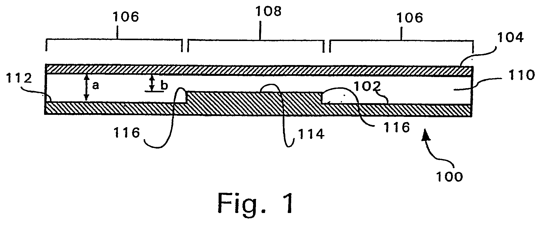
- Fig. 1 and 2 illustrate a dual-band, single layer array 100.
- Fig. 2 is a top view of the array.
- Fig. 1 is a cross-sectional view taken along line 1-1 in Fig. 2.
- Array 100 is comprised of a ground plane 102 and a plurality of antenna elements (not shown) that are disposed on a surface 104.
- a dielectric material 110 is provided in the volume defined between the ground plane 102 and surface 104.
- a plurality of antenna element feed points are preferably provided for each of the antenna elements of the array 100, but have been omitted in Figs. 1 and 2 for greater clarity.
- a first plurality of low frequency antenna elements is preferably disposed in an area 106 of the array and a second plurality of high frequency antenna elements is preferably disposed in an area 108 of the array.
- the ground plane 102 comprises a first effective ground plane portion 112 provided for the first plurality of antenna elements beneath area 106, and a second effective ground plane portion 114 provided beneath area 108 for the second plurality of antenna elements.
- a first spacing "a” between the first effective ground plane portion 112 and the surface 104 is greater as compared to a second spacing "b” between the second effective ground plane portion 114 and surface 104.
- a ground plane stepped portion 116 is provided where the first effective ground plane portion 112 transitions from the first spacing "a” to the second spacing "b” defining the second effective ground plane 114.
- the larger spacing "a" in the area 106 facilitates proper operation of the low frequency antenna elements in this portion of the array 10.
- the smaller spacing "b" in the area 108 facilitates proper operation of the high frequency antenna elements.
- the particular spacing selected in each case will generally be determined by a variety of factors including the operating frequency, the thickness of the antenna elements, and the dielectric constant of the particular dielectric material 110.
- the particular dielectric material 110 selected for use in the present invention is not critical. Any of a variety of commonly used dielectric materials may be used for this purpose, although low loss dielectrics are preferred.
- one suitable class of materials would be polytetrafluoroethylene (PTFE) based composites such as RT/duroid ® 6002 (dielectric constant of 2.94; loss tangent of .009) and RT/duroid ® 5880 (dielectric constant of 2.2; loss tangent of .0007). These products are both available from Rogers Microwave Products, Advanced Circuit Materials Division,100 S. Roosevelt Ave, Chandler, AZ 85226. However, the invention is not limited in this regard.
- the array configuration described in Figs. 1 and 2 is advantageous as it permits antenna arrays for two separate bands of frequencies to be integrated so as to form a single dual-band array with two sets of antenna elements in a common plane defined by surface 104. Designing the frequency response of the high frequency antenna elements to begin approximately where the response of the low frequency antenna elements cuts off can provide an antenna with apparently wider bandwidth. Despite the advantages of the foregoing arrangement, however, use of conventional narrow-band antenna elements in such an array will still result in an overall bandwidth that is somewhat limited. In particular, the limited frequency range of the respective high frequency and low frequency antenna elements used in each array will limit the ultimate combined bandwidth of the array.
- the foregoing limitations can be overcome and further advantage in broadband performance can be achieved by proper selection of antenna elements.
- U.S. Application Serial No. 09/703,247 to Munk et al. entitled Wideband Phased Array Antenna and Associated Methods discloses such a dipole antenna element.
- one embodiment of these elements is illustrated in Fig. 8.
- one or both of the first and second plurality of antenna elements can comprise dipole pairs having a configuration similar to elements 702 in Fig. 8.
- the dipole pairs can have an elongated body portion 802, and an enlarged width end portion 804 connected to an end of the elongated body portion.
- the enlarged width end portions of adjacent ones of the antenna elements comprise interdigitated portions 806. Consequently, an end portion of each dipole element can be capacitively coupled to a corresponding end portion of an adjacent dipole element.
- the low frequency elements used in the array are preferably of a similar geometry and configuration to that shown in Fig. 8, but appropriately sized so as to accommodate the lower frequency band of operation.
- the dipole element of Munk et al. When used in an array, the dipole element of Munk et al., has been found to provide remarkably wideband performance.
- the wideband performance of such antenna elements can be used to advantage in the present invention.
- high frequency band and low frequency band elements of the type described in Munk et al can be disposed in an array as described relative to Figs. 1 and 2 herein.
- the Munk et al. antenna concept benefits from capacitive coupling of individual dipole antenna elements to neighboring antenna elements.
- placing a high frequency cluster in the midst of the low frequency array creates a discontinuity that can interfere with this coupling. This discontinuity can negatively impact on the performance of the low band array if proper precautions are not taken in the overall antenna system design.
- Degradation to the low frequency array can me minimized if the discontinuity created by the high frequency array is relatively small in terms of the wavelength of the low frequency array. In general, a relatively small discontinuous area in the low frequency array will not severely impact the performance of the array.
- the precise maximum area of a discontinuity that can be occupied by the high frequency array without substantial degradation of the low frequency array can be determined experimentally or using computer modeling.
- the discontinuity created by the high frequency array is preferably less than about two (2) wavelength square, where the wavelength is determined based on the operational frequency of the low-band array.
- Figs. 3 and 4 illustrate an alternative embodiment of a dual-band single layer array 300 similar to the arrangement in Figs. 1 and 2.
- Fig. 4 is a top view of the array and
- Fig. 3 is a cross-sectional view taken along line 3-3.
- the array can comprise a plurality of areas108 where high frequency elements are clustered.
- a large distance can separate two or more discontinuous areas 108 forming the high frequency array. This can lead to grating lobe problems if all of the high frequency elements are used concurrently to form a single array.
- the problem can be minimized where the pattern of areas 108 of high frequency clusters is aperiodic.
- an array of elements arranged in an aperiodic lattice can be placed further apart from each other, as compared to a conventional rectangular or triangular lattice, to achieve the same grating-lobe-free scan.
- Grating lobes are a mathematical image of the main beam of a phased array that can appear when the beam of an array is scanned too far. It is dependent on element spacing. If the elements are spaced a half wavelength apart then at that frequency the beam can be scanned anywhere in the hemisphere in front of the array (+/- 90 degrees). If you space the elements one wavelength apart then the grating lobe resides at the edge of visible space and any scanning of the beam will bring the grating lobe fully into visible space. An aperiodic lattice allows the elements to be spaced farther apart and still permit a grating-lobe-free scan.
- the clusters of high frequency elements in areas 108 could be spaced a wavelength or more apart without creating a grating lobe problem.
- the benefits of aperiodic lattices are generally known in the art, but have not generally been applied as described herein.
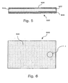
- Fig. 5 is a cross-sectional view of an alternative embodiment of a dual-band, single layer approach.
- Fig. 6 is a top view of the dual-band array of Fig. 5.
- the effective ground plane for the high frequency elements in the array can be provided by a frequency selective surface 502.
- the second effective ground plane 504 for the low frequency elements in the array can be provided by a conventional metal ground plane formed of copper cladding or the like.
- a suitable dielectric material as described above in relation to Figs. 1 and 2 can be provided between the ground plane 504 and the frequency selective surface 502.
- a suitable dielectric material can be provided between the frequency selective surface 502 and the surface 508 on which the antenna elements are disposed.
- the frequency selective surface 502 can be comprised of any layer that is designed to pass the lowband frequencies associated with the low frequency array 704 elements, but is opaque (i.e. acts as a bandstop) for the higher frequency range on which the elements 702 operate. In this regard, it may be desirable to design the frequency selective surface to have a bandstop range of frequencies somewhat higher than the operating range of the higher frequency elements 702 in order to account for anticipated rolloff in the frequency response of the surface.
- a conventional wire or slot arrangement can be used for the frequency selective surface 502, as is known in the art.
- the actual design of a suitable frequency selective surface 502 is well documented in the reference Frequency Selective Surfaces, Ben A. Munk, Copyright 2000 by John Wiley, & Sons .
- the invention is not limited to the specific frequency selective surface disclosed therein. Accordingly, other frequency selective surfaces can also be used for this purpose.
- Fig. 7 is an enlarged schematic representation of the surface 508 showing the interlaced formation of the higher frequency dipole elements 702 and lower frequency dipole elements 704.
- Lower frequency elements 704 and higher frequency elements 702 can be arranged in separate dual polarized grid patterns of spaced rows and columns as shown.
- Feed points 706, 708 are provided for communicating RF to and from the respective elements 702, 704.
- the first and second pluralities of antenna elements are preferably interlaced, rather than arranged in clusters formed in areas 108.
- the interlaced approach does away with the need for the aperiodic clusters and avoids creating a discontinuity in the low frequency array. This can be an advantage as it avoids some of the potential problems associated with grating lobes.
- the disadvantage to this interlaced approach is that both the low frequency and high frequency elements 704, 702 are in very close proximity and can potentially couple to each other.
- the relatively high density of antenna elements etched on the substrate can affect how the elements operate. For example, a few high frequency elements tucked inside a low frequency element will not necessarily perform the same way as the same high frequency elements in isolation.
- the benefits and disadvantages of clustered approach in Figs. 1-4 can therefore be considered and traded off as part of the actual design of a particular array. The best embodiment for a particular application will generally depend upon the requirements that are to be met.
- the number of high frequency elements 702 interposed between the low frequency elements 704 will depend upon the operating frequency and bandwidth of frequencies for the respective low and high frequency elements. In Fig. 7, only four high frequency elements 706 are provided between adjacent low frequency elements 704. However, the invention is not so limited and other configurations are also possible.
- the specific geometry or type of the radiating elements 702, 704 is not critical for dual band operation. According to a preferred embodiment, however, antenna elements having the geometry and characteristics of those disclosed in Munk et al. can be used for achieving a very broad bandwidth. For convenience, one embodiment of the elements as described in Munk et al. is shown in Fig. 8. However, it will be appreciated that other types of antenna elements can also be used for this purpose.
- Antenna elements 704 are preferably of a similar geometry and configuration, but appropriately sized so as to accommodate the lower frequency band of operation.
- Fig. 9 is an example of how the array antennas of Figs. 1-7 can be used.
- a feed controller 802 is conventionally provided for controlling the scanning of a beam formed by the array.
- the feed controller 902 connects the array to transmitting and receiving equipment.
- the feed controller 902 conventionally contains feed lines and phase shifters in communication with the feed points of the respective antenna elements for controlling the scanning of the beam.
Landscapes
- Physics & Mathematics (AREA)
- Electromagnetism (AREA)
- Variable-Direction Aerials And Aerial Arrays (AREA)
- Waveguide Aerials (AREA)
Abstract
Description
- The present invention relates to the field of array antennas and more particularly to array antennas having extremely wide bandwidth.
- Phased array antenna systems are well known in the antenna art. Such antennas are generally comprised of a plurality of radiating elements that are individually controllable with regard to relative phase and amplitude. The antenna pattern of the array is selectively determined by the geometry of the individual elements and the selected phase/amplitude relationships among the elements. Typical radiating elements for such antenna systems may be comprised of dipoles, slots or any other suitable arrangement.
- In recent years, a variety of new planar type antenna elements have been developed which are suitable for use in array applications. One example of such an element is disclosed in U. S. Application Ser. No.
09/703,247 to Munk , et al. - Although the Munk et al. antenna element has a very wide bandwidth for a phased array antenna, there is a continued need and desire for phased array antennas that have even wider bandwidths exceeding 10-to-1. Past efforts to increase the bandwidth of a relatively narrow-band phased array antenna have used various techniques, including dividing the frequency range into multiple bands.
- For example,
U.S. Patent No. 5,485,167 to Wong et al. concerns a multi-frequency phased array antenna using multiple layered dipole arrays. In Wong et al., several layers of dipole pair arrays are provided, each tuned to a different frequency band. The layers are stacked relative to each other along the transmission/reception direction, with the highest frequency array in front of the next lowest frequency array and so forth. In Wong et al., a high band ground screen, comprised of parallel wires disposed in a grid, is disposed between the high-band dipole array and a low band dipole array. - Wong's multiple layer approach has two drawbacks. The dual layer approach makes manufacturing and connecting the elements more difficult due to the embedded interconnects of a multiple layer antenna. Second, in a multiple layer antenna the upper elements will present some amount of blockage to the lower (closer to the ground plane) elements. Moreover, conventional dipole arrays as described in Wong et al. have a relatively narrow bandwidth such that the net result of such configurations may still not provide a sufficiently wideband array. Accordingly, there is a continuing need for improvements in wideband array antennas that have a bandwidth exceeding 10-to-1.
- The invention concerns an array of radiating elements. A first plurality of antenna elements in a first plane in an array configuration is configured for operating on a first band of frequencies. A second plurality of planar antenna elements in an array configuration is configured for operating on a second frequency band, the second plurality of antenna elements is also positioned in the first plane. A first effective ground plane is provided for the first plurality of antenna elements and a second effective ground plane is provided for the second plurality of antenna elements. A first spacing between the first plurality of elements and the first effective ground plane is different from a second spacing between the second plurality of elements and the second effective ground plane. According to one embodiment, the second plurality of elements are adjacent to one another in a unitary cluster that is disposed within the first plurality of elements.
- The array can also comprise a plurality of RF feed points connected to the first and second plurality of antenna elements and a controller for controlling phase and/or amplitude of RF applied to the radiating elements at the feed points. This configuration allows the array to be scanned as needed to advantageously direct the received or transmitted RF energy.
- According to one aspect of the invention, the first plurality of elements can be low band antenna elements for operating on a lower band of frequencies, whereas the second plurality of elements are high band antenna elements for operating on a relatively higher band of frequencies. In that case, the first spacing is greater than the second spacing.
- According to yet another aspect of the invention, the second plurality of antenna elements can define a high frequency cluster or antenna elements. A plurality of such high frequency clusters can be disposed among the first plurality of antenna elements. Each of the high frequency clusters can be configured to operate on the same band of frequencies or can be configured for a band of frequencies distinct from other high frequency clusters.
- A ground plane stepped portion can be provided where the first effective ground plane transitions from the first spacing to the second spacing defining the second effective ground plane. Alternatively, the second effective ground plane can be a low pass frequency selective surface interposed between the second plurality of antenna elements and the first effective ground plane. In any case, at least one dielectric layer is preferably interposed between the first plane, where the first and second plurality of antenna elements are located, and the respective effective ground planes for each set of elements.
- According to one embodiment, one or both of the first and second plurality of antenna elements can comprise an elongated body portion, and an enlarged width end portion connected to an end of the elongated body portion. The enlarged width end portions of adjacent ones of the antenna elements comprise interdigitated portions. More particularly, the plurality of antenna elements can be comprised of adjacent dipole elements, and an end portion of each dipole element can be capacitively coupled to a corresponding end portion of an adjacent dipole element.
- The various features and advantages of the present invention may be more readily understood with reference to the following drawings in which like reference numerals designate like structural elements:
- Fig. 1 is a cross-sectional view of a dual-band, single layer array with a single high frequency cluster.
- Fig. 2 is a top view of the dual band, single layer array of Fig. 1.
- Fig. 3 is a cross-sectional view of a dual-band single layer array with a plurality of high frequency clusters.
- Fig. 4 is a top view of the array in Fig. 3.
- Fig. 5 is a cross-sectional view of an alternative embodiment of a dual band, single layer array.
- Fig. 6 is a top view of the array of Fig. 5.
- Fig. 7 is a schematic representation showing the interlaced formation of the higher and lower frequency elements.
- Fig. 8 is a drawing useful for illustrating an exemplary wideband antenna element for use with the arrays of Figs 1-6.
- Fig. 9 is an example of a phased array antenna system.
- Fig. 1 and 2 illustrate a dual-band,
single layer array 100. Fig. 2 is a top view of the array. Fig. 1 is a cross-sectional view taken along line 1-1 in Fig. 2.Array 100 is comprised of aground plane 102 and a plurality of antenna elements (not shown) that are disposed on asurface 104. Adielectric material 110 is provided in the volume defined between theground plane 102 andsurface 104. A plurality of antenna element feed points are preferably provided for each of the antenna elements of thearray 100, but have been omitted in Figs. 1 and 2 for greater clarity. - According to a preferred embodiment, a first plurality of low frequency antenna elements is preferably disposed in an
area 106 of the array and a second plurality of high frequency antenna elements is preferably disposed in anarea 108 of the array. Theground plane 102 comprises a first effectiveground plane portion 112 provided for the first plurality of antenna elements beneatharea 106, and a second effectiveground plane portion 114 provided beneatharea 108 for the second plurality of antenna elements. - As shown in Fig. 1, a first spacing "a" between the first effective
ground plane portion 112 and thesurface 104 is greater as compared to a second spacing "b" between the second effectiveground plane portion 114 andsurface 104. A ground plane steppedportion 116 is provided where the first effectiveground plane portion 112 transitions from the first spacing "a" to the second spacing "b" defining the secondeffective ground plane 114. - Those skilled in the art will recognize that the larger spacing "a" in the
area 106 facilitates proper operation of the low frequency antenna elements in this portion of the array 10. Conversely, the smaller spacing "b" in thearea 108 facilitates proper operation of the high frequency antenna elements. The particular spacing selected in each case will generally be determined by a variety of factors including the operating frequency, the thickness of the antenna elements, and the dielectric constant of the particulardielectric material 110. - The particular
dielectric material 110 selected for use in the present invention is not critical. Any of a variety of commonly used dielectric materials may be used for this purpose, although low loss dielectrics are preferred. For example, one suitable class of materials would be polytetrafluoroethylene (PTFE) based composites such as RT/duroid ® 6002 (dielectric constant of 2.94; loss tangent of .009) and RT/duroid ® 5880 (dielectric constant of 2.2; loss tangent of .0007). These products are both available from Rogers Microwave Products, Advanced Circuit Materials Division,100 S. Roosevelt Ave, Chandler, AZ 85226. However, the invention is not limited in this regard. - The array configuration described in Figs. 1 and 2 is advantageous as it permits antenna arrays for two separate bands of frequencies to be integrated so as to form a single dual-band array with two sets of antenna elements in a common plane defined by
surface 104. Designing the frequency response of the high frequency antenna elements to begin approximately where the response of the low frequency antenna elements cuts off can provide an antenna with apparently wider bandwidth. Despite the advantages of the foregoing arrangement, however, use of conventional narrow-band antenna elements in such an array will still result in an overall bandwidth that is somewhat limited. In particular, the limited frequency range of the respective high frequency and low frequency antenna elements used in each array will limit the ultimate combined bandwidth of the array. - The foregoing limitations can be overcome and further advantage in broadband performance can be achieved by proper selection of antenna elements.
U.S. Application Serial No. 09/703,247 to Munk et al. entitled Wideband Phased Array Antenna and Associated Methods ("Munk et al.), incorporated herein by reference, discloses such a dipole antenna element. For convenience, one embodiment of these elements is illustrated in Fig. 8. Thus, one or both of the first and second plurality of antenna elements can comprise dipole pairs having a configuration similar toelements 702 in Fig. 8. For example, the dipole pairs can have an elongatedbody portion 802, and an enlargedwidth end portion 804 connected to an end of the elongated body portion. The enlarged width end portions of adjacent ones of the antenna elements comprise interdigitatedportions 806. Consequently, an end portion of each dipole element can be capacitively coupled to a corresponding end portion of an adjacent dipole element. The low frequency elements used in the array are preferably of a similar geometry and configuration to that shown in Fig. 8, but appropriately sized so as to accommodate the lower frequency band of operation. - When used in an array, the dipole element of Munk et al., has been found to provide remarkably wideband performance. The wideband performance of such antenna elements can be used to advantage in the present invention. In particular, high frequency band and low frequency band elements of the type described in Munk et al can be disposed in an array as described relative to Figs. 1 and 2 herein.
- In general, the Munk et al. antenna concept benefits from capacitive coupling of individual dipole antenna elements to neighboring antenna elements. In Figs. 1 and 2, placing a high frequency cluster in the midst of the low frequency array creates a discontinuity that can interfere with this coupling. This discontinuity can negatively impact on the performance of the low band array if proper precautions are not taken in the overall antenna system design.
- Degradation to the low frequency array can me minimized if the discontinuity created by the high frequency array is relatively small in terms of the wavelength of the low frequency array. In general, a relatively small discontinuous area in the low frequency array will not severely impact the performance of the array.
- The precise maximum area of a discontinuity that can be occupied by the high frequency array without substantial degradation of the low frequency array, can be determined experimentally or using computer modeling. However, the discontinuity created by the high frequency array is preferably less than about two (2) wavelength square, where the wavelength is determined based on the operational frequency of the low-band array.
- The foregoing limitations will restrict the maximum preferred size of area defining the discontinuity formed by high frequency array. For example, this factor would limit the size of
area 108 in Fig. 2. If additional high frequency antenna elements are needed to form the high frequency array, then it is necessary to provide a separate discontinuity in the low frequency array some distance away from the first discontinuity. - Figs. 3 and 4 illustrate an alternative embodiment of a dual-band
single layer array 300 similar to the arrangement in Figs. 1 and 2. Fig. 4 is a top view of the array and Fig. 3 is a cross-sectional view taken along line 3-3. As shown in Figs. 3 and 4 the array can comprise a plurality of areas108 where high frequency elements are clustered. - One difficulty associated with the arrangement in Figs. 3 and 4 is that a large distance (electrically) can separate two or more
discontinuous areas 108 forming the high frequency array. This can lead to grating lobe problems if all of the high frequency elements are used concurrently to form a single array. However the problem can be minimized where the pattern ofareas 108 of high frequency clusters is aperiodic. Generally speaking, an array of elements arranged in an aperiodic lattice can be placed further apart from each other, as compared to a conventional rectangular or triangular lattice, to achieve the same grating-lobe-free scan. - Grating lobes are a mathematical image of the main beam of a phased array that can appear when the beam of an array is scanned too far. It is dependent on element spacing. If the elements are spaced a half wavelength apart then at that frequency the beam can be scanned anywhere in the hemisphere in front of the array (+/- 90 degrees). If you space the elements one wavelength apart then the grating lobe resides at the edge of visible space and any scanning of the beam will bring the grating lobe fully into visible space. An aperiodic lattice allows the elements to be spaced farther apart and still permit a grating-lobe-free scan. For example, the clusters of high frequency elements in
areas 108 could be spaced a wavelength or more apart without creating a grating lobe problem. The benefits of aperiodic lattices are generally known in the art, but have not generally been applied as described herein. - Fig. 5 is a cross-sectional view of an alternative embodiment of a dual-band, single layer approach. Fig. 6 is a top view of the dual-band array of Fig. 5. As shown in Fig. 5, the effective ground plane for the high frequency elements in the array can be provided by a frequency
selective surface 502. The secondeffective ground plane 504 for the low frequency elements in the array can be provided by a conventional metal ground plane formed of copper cladding or the like. A suitable dielectric material as described above in relation to Figs. 1 and 2 can be provided between theground plane 504 and the frequencyselective surface 502. Similarly a suitable dielectric material can be provided between the frequencyselective surface 502 and thesurface 508 on which the antenna elements are disposed. - The frequency
selective surface 502 can be comprised of any layer that is designed to pass the lowband frequencies associated with thelow frequency array 704 elements, but is opaque (i.e. acts as a bandstop) for the higher frequency range on which theelements 702 operate. In this regard, it may be desirable to design the frequency selective surface to have a bandstop range of frequencies somewhat higher than the operating range of thehigher frequency elements 702 in order to account for anticipated rolloff in the frequency response of the surface. - According to a preferred embodiment, a conventional wire or slot arrangement can be used for the frequency
selective surface 502, as is known in the art. The actual design of a suitable frequencyselective surface 502 is well documented in the reference Frequency Selective Surfaces, Ben A. Munk, Copyright 2000 by John Wiley, & Sons. However, the invention is not limited to the specific frequency selective surface disclosed therein. Accordingly, other frequency selective surfaces can also be used for this purpose. - Fig. 7 is an enlarged schematic representation of the
surface 508 showing the interlaced formation of the higherfrequency dipole elements 702 and lowerfrequency dipole elements 704.Lower frequency elements 704 andhigher frequency elements 702 can be arranged in separate dual polarized grid patterns of spaced rows and columns as shown. Feed points 706, 708 are provided for communicating RF to and from therespective elements - In the embodiment of Figs. 5-7, the first and second pluralities of antenna elements are preferably interlaced, rather than arranged in clusters formed in
areas 108. The interlaced approach does away with the need for the aperiodic clusters and avoids creating a discontinuity in the low frequency array. This can be an advantage as it avoids some of the potential problems associated with grating lobes. The disadvantage to this interlaced approach is that both the low frequency andhigh frequency elements - The number of
high frequency elements 702 interposed between thelow frequency elements 704 will depend upon the operating frequency and bandwidth of frequencies for the respective low and high frequency elements. In Fig. 7, only fourhigh frequency elements 706 are provided between adjacentlow frequency elements 704. However, the invention is not so limited and other configurations are also possible. - The specific geometry or type of the radiating
elements Antenna elements 704 are preferably of a similar geometry and configuration, but appropriately sized so as to accommodate the lower frequency band of operation. - Fig. 9 is an example of how the array antennas of Figs. 1-7 can be used. A
feed controller 802 is conventionally provided for controlling the scanning of a beam formed by the array. Thefeed controller 902 connects the array to transmitting and receiving equipment. Thefeed controller 902 conventionally contains feed lines and phase shifters in communication with the feed points of the respective antenna elements for controlling the scanning of the beam. - It will be recognized by those skilled in the art that the foregoing embodiments are merely illustrative of the many specific embodiments that represent applications of the invention. Those skilled in the art can readily devise numerous alternative arrangements without departing from the scope of the invention.
Claims (14)
- A unitary array (100) of radiating elements comprising:a first plurality of antenna elements in a first plane (104) in an array configuration, said first plurality of planar antenna elements configured for operating on a first band of frequencies;a second plurality of planar antenna elements in a second array configuration, said second plurality of antenna elements configured for operating on a second band of frequencies, said second plurality of antenna elements positioned in said first plane interposed among said first plurality of planar antenna elements;a first effective ground plane (112) for said first plurality of antenna elements;a second effective ground plane (114) for said second plurality of antenna elements;
characterized in thata first spacing between said first plurality of elements and said first effective ground plane (112) is different from a second spacing between said second plurality of elements and said second effective ground plane (114);at least one of said first and second plurality of antenna elements comprise: an elongated body portion; and an enlarged width end portion connected to an end of the elongated body portion. - The array according to claim 1 wherein said enlarged width end portions of adjacent ones of said antenna elements comprise interdigitated portions.
- The array according to claim 1 wherein at least one of said first and second plurality of antenna elements are comprised of adjacent dipole elements, and an end portion of each dipole element is capacitively coupled to a corresponding end portion of an adjacent dipole element.
- The array according to claim 1 wherein said second plurality of elements are formed adjacent to one another in a cluster, said cluster disposed within said first plurality of elements.
- The array according to claim 1 further comprising: a plurality of RF feed points connected to said first and second plurality of antenna elements; and a controller for controlling at least one of a phase and amplitude of RF applied to said radiating elements at said feed points.
- The array according to claim 1 wherein said first plurality of elements are low band antenna elements for operating on a lower band of frequencies, said second plurality of elements are high band antenna elements for operating on a relatively higher band of frequencies, and said first spacing is greater than said second spacing.
- The array according to claim 1 further comprising a ground plane stepped portion where said first effective ground plane transitions from said first spacing to said second spacing defining said second effective ground plane.
- The array according to claim 1 wherein said second effective ground plane (114) is a low pass frequency selective surface interposed between said second plurality of antenna elements and said first effective ground plane (112).
- The array according to claim 1 wherein said first plurality of antenna elements are interlaced with said second plurality of antenna elements.
- The array according to claim 1 further comprising at least one dielectric layer interposed between said first plane (104), and said first (112) and second (114) effective ground planes.
- The array according to claim 1 wherein said second plurality of antenna elements defines a high frequency cluster, and said array comprises a plurality of said high frequency clusters disposed among said first plurality of antenna elements.
- The array according to claim 11, wherein said high frequency clusters are disposed in an aperiodic pattern.
- The array according to claim 1, comprising:said first plurality of antenna elements positioned adjacent to one another in an array;said second plurality of planar antenna elements adjacent to one another in an array configuration and forming a cluster within said first plurality of antenna elements,and configured for operating on a second band of frequencies distinct from said first band of frequencies;wherein said first plurality of elements are low band antenna elements for operating on a lower band of frequencies, said second plurality of elements are high band antenna elements for operating on a relatively higher band of frequencies.
- The array according to claim 1, comprising:said first plurality of antenna elements positioned adjacent to one another in an array;said second plurality of planar antenna elements adjacent to one another in an array configuration, said second plurality of antenna elements positioned in said first plane interlaced among said first plurality of planar antenna elements and configured for operating on a second band of frequencies distinct from said first band of frequencies; andwherein said second effective ground plane is a low pass frequency selective surface interposed between said second plurality of antenna elements and said first effective ground plane.
Applications Claiming Priority (2)
| Application Number | Priority Date | Filing Date | Title |
|---|---|---|---|
| US10/052,288 US6552687B1 (en) | 2002-01-17 | 2002-01-17 | Enhanced bandwidth single layer current sheet antenna |
| EP03702090A EP1468471B1 (en) | 2002-01-17 | 2003-01-14 | Enhanced bandwidth single layer current sheet antenna |
Related Parent Applications (1)
| Application Number | Title | Priority Date | Filing Date |
|---|---|---|---|
| EP03702090A Division EP1468471B1 (en) | 2002-01-17 | 2003-01-14 | Enhanced bandwidth single layer current sheet antenna |
Publications (2)
| Publication Number | Publication Date |
|---|---|
| EP1777780A2 true EP1777780A2 (en) | 2007-04-25 |
| EP1777780A3 EP1777780A3 (en) | 2007-05-16 |
Family
ID=21976619
Family Applications (2)
| Application Number | Title | Priority Date | Filing Date |
|---|---|---|---|
| EP06026197A Withdrawn EP1777780A3 (en) | 2002-01-17 | 2003-01-14 | Enhanced bandwidth single layer current sheet antenna |
| EP03702090A Expired - Lifetime EP1468471B1 (en) | 2002-01-17 | 2003-01-14 | Enhanced bandwidth single layer current sheet antenna |
Family Applications After (1)
| Application Number | Title | Priority Date | Filing Date |
|---|---|---|---|
| EP03702090A Expired - Lifetime EP1468471B1 (en) | 2002-01-17 | 2003-01-14 | Enhanced bandwidth single layer current sheet antenna |
Country Status (11)
| Country | Link |
|---|---|
| US (1) | US6552687B1 (en) |
| EP (2) | EP1777780A3 (en) |
| JP (1) | JP4025728B2 (en) |
| KR (1) | KR100635530B1 (en) |
| CN (1) | CN1618144A (en) |
| AU (1) | AU2003202974B2 (en) |
| CA (1) | CA2468962A1 (en) |
| DE (1) | DE60318011T2 (en) |
| NO (1) | NO20042457L (en) |
| TW (1) | TWI240457B (en) |
| WO (1) | WO2003063295A1 (en) |
Families Citing this family (50)
| Publication number | Priority date | Publication date | Assignee | Title |
|---|---|---|---|---|
| ES2205898T3 (en) | 1999-10-26 | 2004-05-01 | Fractus, S.A. | MULTIBAND CLUSTERS OF INTERRELATED ANTENNAS. |
| US6856297B1 (en) * | 2003-08-04 | 2005-02-15 | Harris Corporation | Phased array antenna with discrete capacitive coupling and associated methods |
| US6903703B2 (en) * | 2003-11-06 | 2005-06-07 | Harris Corporation | Multiband radially distributed phased array antenna with a sloping ground plane and associated methods |
| US6956532B2 (en) * | 2003-11-06 | 2005-10-18 | Harris Corporation | Multiband radially distributed phased array antenna with a stepped ground plane and associated methods |
| US6943748B2 (en) * | 2003-11-06 | 2005-09-13 | Harris Corporation | Multiband polygonally distributed phased array antenna and associated methods |
| US6954179B2 (en) * | 2003-11-06 | 2005-10-11 | Harris Corporation | Multiband radially distributed graded phased array antenna and associated methods |
| US6894655B1 (en) * | 2003-11-06 | 2005-05-17 | Harris Corporation | Phased array antenna with selective capacitive coupling and associated methods |
| US7190315B2 (en) * | 2003-12-18 | 2007-03-13 | Intel Corporation | Frequency selective surface to suppress surface currents |
| US20050134521A1 (en) * | 2003-12-18 | 2005-06-23 | Waltho Alan E. | Frequency selective surface to suppress surface currents |
| US6958738B1 (en) | 2004-04-21 | 2005-10-25 | Harris Corporation | Reflector antenna system including a phased array antenna having a feed-through zone and related methods |
| US6965355B1 (en) * | 2004-04-21 | 2005-11-15 | Harris Corporation | Reflector antenna system including a phased array antenna operable in multiple modes and related methods |
| US6999044B2 (en) * | 2004-04-21 | 2006-02-14 | Harris Corporation | Reflector antenna system including a phased array antenna operable in multiple modes and related methods |
| WO2006024516A1 (en) | 2004-08-31 | 2006-03-09 | Fractus, S.A. | Slim multi-band antenna array for cellular base stations |
| WO2006035881A1 (en) * | 2004-09-30 | 2006-04-06 | Toto Ltd. | Microstrip antenna and high frequency sensor using microstrip antenna |
| EP1935057B1 (en) | 2005-10-14 | 2012-02-01 | Fractus S.A. | Slim triple band antenna array for cellular base stations |
| US8195118B2 (en) | 2008-07-15 | 2012-06-05 | Linear Signal, Inc. | Apparatus, system, and method for integrated phase shifting and amplitude control of phased array signals |
| GB2469075A (en) | 2009-03-31 | 2010-10-06 | Univ Manchester | Wide band array antenna |
| US8872719B2 (en) | 2009-11-09 | 2014-10-28 | Linear Signal, Inc. | Apparatus, system, and method for integrated modular phased array tile configuration |
| US8558749B2 (en) | 2010-04-28 | 2013-10-15 | Bae Systems Information And Electronic Systems Integration Inc. | Method and apparatus for elimination of duplexers in transmit/receive phased array antennas |
| CN102394349B (en) * | 2011-07-08 | 2014-12-10 | 电子科技大学 | Octagonal-ring plane bipolarized broadband phased-array antenna based on strong mutual coupling effects |
| US20130154899A1 (en) * | 2011-12-19 | 2013-06-20 | William Lynn Lewis, III | Aperiodic distribution of aperture elements in a dual beam array |
| US9680232B2 (en) * | 2012-05-07 | 2017-06-13 | Qualcomm Incorporated | Graded-ground design in a millimeter-wave radio module |
| GB201314242D0 (en) | 2013-08-08 | 2013-09-25 | Univ Manchester | Wide band array antenna |
| EP3033804B1 (en) * | 2013-08-16 | 2020-12-02 | Intel Corporation | Millimeter wave antenna structures with air-gap layer or cavity |
| US9667290B2 (en) * | 2015-04-17 | 2017-05-30 | Apple Inc. | Electronic device with millimeter wave antennas |
| US9991605B2 (en) | 2015-06-16 | 2018-06-05 | The Mitre Corporation | Frequency-scaled ultra-wide spectrum element |
| US10056699B2 (en) | 2015-06-16 | 2018-08-21 | The Mitre Cooperation | Substrate-loaded frequency-scaled ultra-wide spectrum element |
| SE539136C2 (en) * | 2015-10-09 | 2017-04-11 | Qamcom Tech Ab | Method and antenna array apparatus |
| US11367959B2 (en) | 2015-10-28 | 2022-06-21 | Rogers Corporation | Broadband multiple layer dielectric resonator antenna and method of making the same |
| US10374315B2 (en) | 2015-10-28 | 2019-08-06 | Rogers Corporation | Broadband multiple layer dielectric resonator antenna and method of making the same |
| US10476164B2 (en) | 2015-10-28 | 2019-11-12 | Rogers Corporation | Broadband multiple layer dielectric resonator antenna and method of making the same |
| US10601137B2 (en) | 2015-10-28 | 2020-03-24 | Rogers Corporation | Broadband multiple layer dielectric resonator antenna and method of making the same |
| IT201600130208A1 (en) * | 2016-12-22 | 2018-06-22 | Eggtronic Eng S R L | Wireless power transfer system |
| US11283189B2 (en) | 2017-05-02 | 2022-03-22 | Rogers Corporation | Connected dielectric resonator antenna array and method of making the same |
| US11876295B2 (en) | 2017-05-02 | 2024-01-16 | Rogers Corporation | Electromagnetic reflector for use in a dielectric resonator antenna system |
| KR102312067B1 (en) | 2017-06-07 | 2021-10-13 | 로저스코포레이션 | Dielectric Resonator Antenna System |
| US10854993B2 (en) | 2017-09-18 | 2020-12-01 | The Mitre Corporation | Low-profile, wideband electronically scanned array for geo-location, communications, and radar |
| US11616302B2 (en) | 2018-01-15 | 2023-03-28 | Rogers Corporation | Dielectric resonator antenna having first and second dielectric portions |
| US10892544B2 (en) | 2018-01-15 | 2021-01-12 | Rogers Corporation | Dielectric resonator antenna having first and second dielectric portions |
| US10910722B2 (en) | 2018-01-15 | 2021-02-02 | Rogers Corporation | Dielectric resonator antenna having first and second dielectric portions |
| US10886625B2 (en) | 2018-08-28 | 2021-01-05 | The Mitre Corporation | Low-profile wideband antenna array configured to utilize efficient manufacturing processes |
| US11552390B2 (en) | 2018-09-11 | 2023-01-10 | Rogers Corporation | Dielectric resonator antenna system |
| US11031697B2 (en) | 2018-11-29 | 2021-06-08 | Rogers Corporation | Electromagnetic device |
| JP2022510892A (en) | 2018-12-04 | 2022-01-28 | ロジャーズ コーポレーション | Dielectric electromagnetic structure and its manufacturing method |
| US11482790B2 (en) | 2020-04-08 | 2022-10-25 | Rogers Corporation | Dielectric lens and electromagnetic device with same |
| US11688944B2 (en) * | 2020-10-26 | 2023-06-27 | KYOCERA AVX Components (San Diego), Inc. | Wideband phased array antenna for millimeter wave communications |
| CN112736449B (en) * | 2021-03-30 | 2021-07-06 | 成都天锐星通科技有限公司 | Dual-frequency common-aperture antenna structure and antenna array surface |
| CN116632540A (en) * | 2022-02-18 | 2023-08-22 | 联发科技股份有限公司 | antenna system |
| US12374810B2 (en) * | 2022-02-18 | 2025-07-29 | Mediatek Inc. | Antenna system for accessing wireless signal of multiple frequency band |
| DE112022007376T5 (en) * | 2022-06-15 | 2025-05-08 | Beijing Boe Sensor Technology Co., Ltd. | DUAL-FREQUENCY ANTENNA AND ELECTRONIC DEVICE |
Family Cites Families (14)
| Publication number | Priority date | Publication date | Assignee | Title |
|---|---|---|---|---|
| US3710337A (en) * | 1970-03-24 | 1973-01-09 | Jfd Electronics Corp | Miniature tv antenna |
| US3747114A (en) * | 1972-02-18 | 1973-07-17 | Textron Inc | Planar dipole array mounted on dielectric substrate |
| US3761943A (en) * | 1972-07-21 | 1973-09-25 | Us Navy | Dual-band array antenna |
| WO1988009065A1 (en) * | 1987-05-08 | 1988-11-17 | Darrell Coleman | Broad frequency range aerial |
| FR2640431B1 (en) * | 1988-12-08 | 1991-05-10 | Alcatel Espace | MULTI-FREQUENCY RADIANT DEVICE |
| US5087922A (en) | 1989-12-08 | 1992-02-11 | Hughes Aircraft Company | Multi-frequency band phased array antenna using coplanar dipole array with multiple feed ports |
| US5485167A (en) | 1989-12-08 | 1996-01-16 | Hughes Aircraft Company | Multi-frequency band phased-array antenna using multiple layered dipole arrays |
| CA2030963C (en) * | 1989-12-14 | 1995-08-15 | Robert Michael Sorbello | Orthogonally polarized dual-band printed circuit antenna employing radiating elements capacitively coupled to feedlines |
| FR2760133B1 (en) * | 1997-02-24 | 1999-03-26 | Alsthom Cge Alcatel | RESONANT ANTENNA FOR THE TRANSMISSION OR RECEPTION OF POLARIZED WAVES |
| US6057802A (en) * | 1997-06-30 | 2000-05-02 | Virginia Tech Intellectual Properties, Inc. | Trimmed foursquare antenna radiating element |
| US6175333B1 (en) * | 1999-06-24 | 2001-01-16 | Nortel Networks Corporation | Dual band antenna |
| US6211841B1 (en) * | 1999-12-28 | 2001-04-03 | Nortel Networks Limited | Multi-band cellular basestation antenna |
| US6452549B1 (en) * | 2000-05-02 | 2002-09-17 | Bae Systems Information And Electronic Systems Integration Inc | Stacked, multi-band look-through antenna |
| US6483481B1 (en) * | 2000-11-14 | 2002-11-19 | Hrl Laboratories, Llc | Textured surface having high electromagnetic impedance in multiple frequency bands |
-
2002
- 2002-01-17 US US10/052,288 patent/US6552687B1/en not_active Expired - Fee Related
- 2002-12-31 TW TW091138050A patent/TWI240457B/en not_active IP Right Cessation
-
2003
- 2003-01-14 AU AU2003202974A patent/AU2003202974B2/en not_active Expired - Fee Related
- 2003-01-14 CA CA002468962A patent/CA2468962A1/en not_active Abandoned
- 2003-01-14 DE DE60318011T patent/DE60318011T2/en not_active Expired - Fee Related
- 2003-01-14 KR KR1020047011099A patent/KR100635530B1/en not_active Expired - Fee Related
- 2003-01-14 JP JP2003563046A patent/JP4025728B2/en not_active Expired - Fee Related
- 2003-01-14 WO PCT/US2003/000960 patent/WO2003063295A1/en not_active Ceased
- 2003-01-14 EP EP06026197A patent/EP1777780A3/en not_active Withdrawn
- 2003-01-14 CN CNA038023946A patent/CN1618144A/en active Pending
- 2003-01-14 EP EP03702090A patent/EP1468471B1/en not_active Expired - Lifetime
-
2004
- 2004-06-14 NO NO20042457A patent/NO20042457L/en not_active Application Discontinuation
Also Published As
| Publication number | Publication date |
|---|---|
| AU2003202974B2 (en) | 2005-08-18 |
| DE60318011T2 (en) | 2008-12-04 |
| TW200305302A (en) | 2003-10-16 |
| KR20040070316A (en) | 2004-08-06 |
| NO20042457L (en) | 2004-07-28 |
| EP1468471B1 (en) | 2007-12-12 |
| EP1777780A3 (en) | 2007-05-16 |
| US6552687B1 (en) | 2003-04-22 |
| TWI240457B (en) | 2005-09-21 |
| WO2003063295A1 (en) | 2003-07-31 |
| EP1468471A4 (en) | 2005-04-13 |
| CA2468962A1 (en) | 2003-07-31 |
| CN1618144A (en) | 2005-05-18 |
| JP4025728B2 (en) | 2007-12-26 |
| DE60318011D1 (en) | 2008-01-24 |
| EP1468471A1 (en) | 2004-10-20 |
| JP2005516447A (en) | 2005-06-02 |
| KR100635530B1 (en) | 2006-10-19 |
Similar Documents
| Publication | Publication Date | Title |
|---|---|---|
| AU2003202974B2 (en) | Enhanced bandwidth single layer current sheet antenna | |
| AU2003202974A1 (en) | Enhanced bandwidth single layer current sheet antenna | |
| EP1650829B1 (en) | Enhanced bandwidth dual layer sheet antenna | |
| AU755012B2 (en) | Broadband fixed-radius slot antenna arrangement | |
| EP0207029B1 (en) | Electromagnetically coupled microstrip antennas having feeding patches capacitively coupled to feedlines | |
| WO2017161611A1 (en) | Multi-band single feed dielectric resonator antenna (dra) array | |
| CN114069219A (en) | Microstrip phased array antenna unit and its array | |
| EP1751826B1 (en) | Closely packed dipole array antenna | |
| US5633646A (en) | Mini-cap radiating element | |
| KR20050117316A (en) | Microstrip stack patch antenna using multi-layered metallic disk and a planar array antenna using it | |
| EP0450881A2 (en) | Microstrip antennas | |
| CN106505310A (en) | Low-profile array antenna with broadband and wide-angle scanning characteristics | |
| KR101857388B1 (en) | High gain antenna device acting in dual band frequencly | |
| WO2022081092A1 (en) | Metasurface radiator | |
| Jang et al. | Highly compact and high gain 2 x 2 patch array antenna with slotted meanderline Loading | |
| AU2003202973A1 (en) | Enhanced bandwidth dual layer current sheet antenna | |
| KR20250124774A (en) | Patch antenna | |
| WO2007060477A2 (en) | Notch antenna element and array |
Legal Events
| Date | Code | Title | Description |
|---|---|---|---|
| PUAI | Public reference made under article 153(3) epc to a published international application that has entered the european phase |
Free format text: ORIGINAL CODE: 0009012 |
|
| PUAL | Search report despatched |
Free format text: ORIGINAL CODE: 0009013 |
|
| 17P | Request for examination filed |
Effective date: 20061218 |
|
| AC | Divisional application: reference to earlier application |
Ref document number: 1468471 Country of ref document: EP Kind code of ref document: P |
|
| AK | Designated contracting states |
Kind code of ref document: A2 Designated state(s): DE FR GB IT SE |
|
| AK | Designated contracting states |
Kind code of ref document: A3 Designated state(s): DE FR GB IT SE |
|
| AKX | Designation fees paid |
Designated state(s): DE FR GB IT SE |
|
| 17Q | First examination report despatched |
Effective date: 20080207 |
|
| GRAP | Despatch of communication of intention to grant a patent |
Free format text: ORIGINAL CODE: EPIDOSNIGR1 |
|
| STAA | Information on the status of an ep patent application or granted ep patent |
Free format text: STATUS: THE APPLICATION IS DEEMED TO BE WITHDRAWN |
|
| 18D | Application deemed to be withdrawn |
Effective date: 20090325 |