EP1775832A1 - High-efficiency power amplifier - Google Patents
High-efficiency power amplifier Download PDFInfo
- Publication number
- EP1775832A1 EP1775832A1 EP06117200A EP06117200A EP1775832A1 EP 1775832 A1 EP1775832 A1 EP 1775832A1 EP 06117200 A EP06117200 A EP 06117200A EP 06117200 A EP06117200 A EP 06117200A EP 1775832 A1 EP1775832 A1 EP 1775832A1
- Authority
- EP
- European Patent Office
- Prior art keywords
- power amplifier
- power
- low
- input
- amplifier
- Prior art date
- Legal status (The legal status is an assumption and is not a legal conclusion. Google has not performed a legal analysis and makes no representation as to the accuracy of the status listed.)
- Granted
Links
Images



Classifications
-
- H—ELECTRICITY
- H03—ELECTRONIC CIRCUITRY
- H03F—AMPLIFIERS
- H03F3/00—Amplifiers with only discharge tubes or only semiconductor devices as amplifying elements
- H03F3/20—Power amplifiers, e.g. Class B amplifiers, Class C amplifiers
-
- H—ELECTRICITY
- H03—ELECTRONIC CIRCUITRY
- H03F—AMPLIFIERS
- H03F1/00—Details of amplifiers with only discharge tubes, only semiconductor devices or only unspecified devices as amplifying elements
- H03F1/02—Modifications of amplifiers to raise the efficiency, e.g. gliding Class A stages, use of an auxiliary oscillation
- H03F1/0205—Modifications of amplifiers to raise the efficiency, e.g. gliding Class A stages, use of an auxiliary oscillation in transistor amplifiers
- H03F1/0211—Modifications of amplifiers to raise the efficiency, e.g. gliding Class A stages, use of an auxiliary oscillation in transistor amplifiers with control of the supply voltage or current
- H03F1/0216—Continuous control
- H03F1/0222—Continuous control by using a signal derived from the input signal
-
- H—ELECTRICITY
- H03—ELECTRONIC CIRCUITRY
- H03F—AMPLIFIERS
- H03F1/00—Details of amplifiers with only discharge tubes, only semiconductor devices or only unspecified devices as amplifying elements
- H03F1/02—Modifications of amplifiers to raise the efficiency, e.g. gliding Class A stages, use of an auxiliary oscillation
- H03F1/0205—Modifications of amplifiers to raise the efficiency, e.g. gliding Class A stages, use of an auxiliary oscillation in transistor amplifiers
- H03F1/0277—Selecting one or more amplifiers from a plurality of amplifiers
-
- H—ELECTRICITY
- H03—ELECTRONIC CIRCUITRY
- H03F—AMPLIFIERS
- H03F1/00—Details of amplifiers with only discharge tubes, only semiconductor devices or only unspecified devices as amplifying elements
- H03F1/32—Modifications of amplifiers to reduce non-linear distortion
Definitions
- the present invention relates to a power amplifier, and more particularly, to a power amplifier of a low-power consumption system that has linearity at peak output while increasing efficiency in a most frequently used range, and thus enabling a battery to last longer.
- mobile communication terminals In general, mobile communication terminals, cellular phones, and non-constant envelope systems (for example, code division multiple access (CDMA), wideband-CDMA (W-CDMA), etc.), in which linearity is an important requirement, usually employ class A or class AB power amplifiers.
- CDMA code division multiple access
- W-CDMA wideband-CDMA
- class A class AB power amplifiers
- core technology on the rise includes chip miniaturization, analog device gain improvement, leakage current prevention, multi-operating voltage and clock gating circuit design, mixed-mode communication, intelligent transmission protocol, and so forth.
- a power amplifier which is an indispensable component for transmitting a signal, consumes the most power in a portable mobile communication terminal. Therefore, if a power amplifier circuit used in a mobile communication terminal and a cellular phone is manufactured in such a way that it consumes less power, the result is a low-power consumption system with multiple and complex functions.
- Such a system can vitalize the mobile communication service industry and provides individuals with many daily activity functions through just one terminal. Furthermore, since multimedia communication using a terminal can proceed for a longer time, restrictions of space and time can be better overcome and the free flow of information throughout society can be enhanced.
- FIG. 1 is a schematic block diagram illustrating a conventional power amplifier.
- the conventional power amplifier comprises a high-power amplification device 1 amplifying an input radio frequency (RF) signal; a mode switch 2 determining consumption currents I 1 and I 2 of the high-power amplification device 1; and an input impedance matching circuit 3 and an output impedance matching circuit 4 for matching the input and output impedances of the high-power amplification device 1.
- RF radio frequency
- a heterojunction bipolar transistor (HBT) array is mainly used for the high-power amplification device 1, which can be a bipolar junction transistor (BJT) array, field effect transistor (FET) array, and so forth.
- BJT bipolar junction transistor
- FET field effect transistor
- a power amplifier when an RF output power is less than a direct current (DC) consumption power, a power amplifier shows very low power efficiency.
- the conventional power amplifier operates in a high-power mode and a low-power mode in which less power is consumed.
- the consumption currents I 1 and I 2 in the high-power mode and low-power mode are determined by the mode switch 2, and a supply voltage is determined to be a battery supply voltage (in cellular phones, about 3.4V to 4.2V). Therefore, power consumption is determined by supplied DC current.
- a voltage swing range for generating the peak output power becomes the battery supply voltage, and a load impedance of about 2 to 5 Ohms is used according to a current swing range.
- a load impedance at the maximum efficiency is more than about 150hms. Therefore, when the same output impedance is shared between the high-power mode and low-power mode, a consumption current at an operating point is changed by mode switching in both modes, but the peak output power should be satisfied first. Therefore, a load impedance is designed to be appropriate for the high-power mode, so that efficiency in the low-power mode in which an RF input is less than about 16dBm is hardly more than about 10%.
- FIG. 2 is a graph showing Conexant company's use rate function according to output power.
- an output power use rate is as shown in FIG. 2, such as in a mobile communication terminal/cellular phone, a power amplifier operating with maximum efficiency at the peak output power has a problem in that a power-added efficiency drops in an area between about-16dBm and 16dBm that has a high use rate.
- One aspect of the present invention provides a power amplifier comprising an input impedance matcher for impedance-matching a signal input from the outside; a high-power amplifier and a low-power amplifier for amplifying the signal having passed through the input impedance matcher; an amplification controller for controlling the high-power amplifier and low-power amplifier according to a power level of the input signal; an output impedance matcher for impedance-matching the signal amplified by the high-powder amplifier and low-power amplifier; and a dynamic voltage supplier for supplying the low-power amplifier with a variable driving voltage.
- the power amplifier may further comprise a first amplifier for amplifying the signal matched by the input impedance matcher, and a middle-stage impedance matcher for impedance-matching the signal amplified by the first amplifier and sending the impedance matched signal to the high-power and low-power amplifiers.
- the high-power amplifier may operate in a high-power mode for a highest power consumption range, and the low-power amplifier may operate in a low-power mode for a most frequently used range.
- FIG. 1 is a schematic block diagram illustrating a conventional power amplifier
- FIG. 2 is a graph showing Conexant company's use rate function according to output power
- FIG. 3 is a block diagram illustrating the overall structure of a power amplifier according to a first exemplary embodiment of the present invention
- FIG. 4 is a circuit diagram illustrating a third amplifier of FIG. 3 in detail
- FIG. 5 is a circuit diagram illustrating a dynamic voltage supplier of FIG.3 in detail
- FIG. 6 is a graph of output voltage versus input power of the dynamic voltage supplier shown in FIG. 3;
- FIG. 7 is a graph of efficiency versus output power of the power amplifier according to the first exemplary embodiment of the present invention.
- FIG. 8 is a graph of an adjacent channel leakage ratio versus output power of the power amplifier according to the first exemplary embodiment of the present invention.
- FIG. 9 is a block diagram illustrating the overall structure of a power amplifier according to a second exemplary embodiment of the present invention.
- FIG. 3 is a block diagram illustrating the overall structure of a power amplifier according to a first exemplary embodiment of the present invention
- FIG. 4 is a circuit diagram illustrating a third amplifier of FIG. 3 in detail
- FIG. 5 is a circuit diagram illustrating a dynamic voltage supplier of FIG.3 in detail.
- the high-efficiency mixed-mode power amplifier according to the first exemplary embodiment of the present invention comprises an input impedance matcher 100, a first amplifier 200, a middle stage impedance matcher 300, a high-power amplifier 400, a low-power amplifier 500, an output impedance matcher 600, an amplifier controller 700, and a dynamic voltage supplier 800.
- the input impedance matcher 100 impedance-matches a radio frequency (RF) signal input from the outside and outputs the impedance-matched signal.
- RF radio frequency
- the first amplifier 200 receives and amplifies the signal output from the input impedance matcher 100.
- the middle stage impedance matcher 300 receives the amplified signal from the first amplifier 200, and properly impedance-matches and outputs the signal.
- the high-power amplifier 400 is a high-linearity amplifier, operates according to control of the amplifier controller 700 in a high-power mode and in a highest power consumption range, and receives and amplifies the signal output from the middle stage impedance matcher 300.
- the size of the high-power amplifier 400 is larger than that of the first amplifier 200 and the low-power amplifier 500.
- the low-power amplifier 500 is a non-linear amplifier, operates according to control of the amplifier controller 700 in a low-power mode and in a most frequently used range, is connected with the high-power amplifier 400 in parallel, and receives and amplifies the signal output from the middle stage impedance matcher 300.
- the low-power amplifier 500 is, for example, a class E amplifier, and includes a bias unit 510, a first transistor T1, and a class E load 520 in order to obtain a high-efficiency characteristic.
- the bias unit 10 is connected to the output terminal of the amplifier controller 700, and turns the low-power amplifier 500 on and off.
- the first transistor T1 operates according to a control signal of the amplifier controller 700.
- the class E load 520 is connected between the collector of the first transistor T1 and the input terminal of the output impedance matcher 600, and inputs the RF signal to the output impedance matcher 600.
- the collector of the first transistor T1 is connected to the dynamic voltage supplier 800, and the emitter of the first transistor T1 is grounded.
- the output impedance matcher 600 impedance-matches the signal amplified by the high-power amplifier 400 or the low-power amplifier 500, and outputs the optimized signal.
- the amplifier controller 700 controls the high-power amplifier 400 and low-power amplifier 500 by transferring the digital signal according to the high-power mode or low-power mode, applying a general digital-signal control technique.
- the amplifier controller 700 generates the predetermined power control signal on the basis of an antenna output signal from the outside. And then, when the amplifier controller 700 operates in the high-power mode, it controls the low-power amplifier 500 to be turned off so as not to operate and controls only the high-power amplifier 400 to be turned on so as to operate. On the other hand, when the amplifier controller 700 operates in the low-power mode, it controls the high-power amplifier 400 to be turned off and only the low-power amplifier 500 to be turned on so as to operate.
- the dynamic voltage supplier 800 is connected between the input impedance matcher 100 and the first amplifier 200 and supplies the low-power amplifier 500 with voltage in the low-power mode and in the most frequently used range. In other words, the low-power amplifier 500 is driven by the dynamic voltage supplier 800. In addition, the same effect can be obtained even if the dynamic voltage supplier 800 is connected to any point ahead of the high-power and low-powder amplifiers 400 and 500 to which the input signal is sent, such as between the first amplifier 200 and the high-power amplifier 400 or between the first amplifier 200 and the low-power amplifier 500 (not shown in FIG. 3). In other words, connected as described above, the dynamic voltage supplier 800 is affected by an input power P in , and thus smoothly performs its function.
- the dynamic voltage supplier 800 includes a first capacitor C1, a second transistor T2, a first resistor R1, a second capacitor C2, a third transistor T3, a second resistor R2, a third resistor R3, and a transformer 850.
- the first capacitor C1 is connected between an input power P in terminal and a bias voltage V bias terminal, and the second transistor T2 operates according to the input power P in .
- the first resistor R1 is connected between the collector of the second transistor T2 and a collector voltage Vcc terminal.
- the second capacitor C2 is connected between the collector of the second transistor T2 and ground, and the third transistor T3 operates according to a collector potential of the second transistor T2.
- the second resistor R2 is connected between the collector of the third transistor T3 and the collector voltage Vcc terminal, and the third resistor R3 is connected between the emitter of the third transistor T3 and ground.
- the transformer 850 is connected between the collector of the third transistor T3 and an output voltage terminal, that is, the low-power amplifier 500.
- the transformer 850 is for increasing an impedance, and may further include a predetermined load 900 of which one end is connected between the transformer 850 and the low-power amplifier 500 and the other end is grounded.
- the input power P in terminal is connected between the input impedance matcher 100 and the first amplifier 200, the emitter of the second transistor T2 is grounded, and the collector of the second transistor T2 is connected with the base of the third transistor T3.
- a base voltage of the third transistor T3 is reduced by a current of the second transistor T2, which increases according to the input power P in .
- the third transistor T3 is turned off, so that an output voltage is determined by the impedance of the second resistor R2 and the load 900.
- a point where the third transistor T3 is affected by the input power P in in the dynamic voltage supplier 800, and the inclination of the DC output voltage that increases according to the input power P in are preferably determined by the values of the first, second and third resistors R1, R2 and R3 and the emitter dimension of the second transistor T2.
- the RF signal input through the common input impedance matcher 100 is amplified by a predetermined level by the first amplifier 200 while passing along a power control path, is impedance-matched by the middle stage impedance matcher 300, and is output to the high-power and low-power amplifiers 400 and 500 that respectively operate in the high-power and low-power modes.
- FIG. 6 is a graph of output voltage versus input power of the dynamic voltage supplier shown in FIG. 3.
- PAE power added efficiency
- the high-efficiency mixed-mode power amplifier uses the high-power amplifier 400, which is a high-linearity power amplifier, to obtain high linearity at high power, and uses the low-power amplifier 500, which is a non-linear amplifier, to obtain high efficiency at low power.
- the efficiency of the power amplifier can be maximized by maintaining the minimum output voltage of the dynamic voltage supplier 800 in the low-power mode.
- FIG. 6 shows output voltage versus input power when the driving voltage Vcc of the device is about 3V in the dynamic voltage supplier 800.
- FIG. 6 indicates that the output voltage is low in the low-power mode, increases as the input power increases, that is, as the power amplifier shifts to the high-power mode, and is fixed after the input power exceeds the predetermined value.
- the voltage applied to the low-power amplifier 500 is controlled to be low at the same operating voltage Vcc in the low-power mode in which the input power is low, the input DC power is reduced. Hereupon, the power added efficiency of the low-power amplifier 500 is maximized.
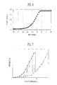
- FIG. 7 is a graph of efficiency versus output power of the power amplifier according to the first exemplary embodiment of the present invention.
- a linear power amplifier such as a conventional power amplifier (or a large-sized amplifier) shows a low efficiency at an output power of less than 16dBm, as represented by a dotted line.
- the first exemplary embodiment of the present invention yields improvement in efficiency in a frequently used output powder range due to the influence of the low-power amplifier 500, which is a small-sized non-linear amplifier, and the dynamic voltage supplier 800.
- power added efficiency in the low-power mode can be maximized to a level similar to the efficiency corresponding to the peak output power.
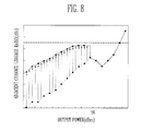
- FIG. 8 is a graph of an adjacent channel leakage ratio versus output power of the power amplifier according to the first exemplary embodiment of the present invention.
- the adjacent channel leakage ratio is sufficiently far from a standard that there is no need to consider the linearity of the conventional linear amplifier (or a large-sized amplifier) in a low-output-power area.
- the linearity seriously deteriorates at an output power of less than 16dBm due to the low-power amplifier 500, which is a small-sized non-linear amplifier and operates in the low-power mode.
- an adjacent channel leakage ratio is an index indicating the linearity of a power amplifier, and is defined as the linearity standard of a power amplifier in a wideband code division multiple access (W-CDMA) method.
- W-CDMA wideband code division multiple access
- an ACLR standard is satisfied using the high-power amplifier 400, which is a large-sized linear amplifier.
- the ACLR increases due to the low-power amplifier 500, which is a small-sized, non-linear amplifier, but is restricted to less than required by the standard, so that linearity can be maintained.
- FIG. 9 is a block diagram illustrating the overall structure of a power amplifier according to a second exemplary embodiment of the present invention.
- the power amplifier according to the second exemplary embodiment of the present invention has a constitution similar to the first exemplary embodiment. Therefore, many aspects of the second exemplary embodiment can be understood by referring to the first exemplary embodiment.
- the power amplifier according to the second exemplary embodiment of the present invention is different from the power amplifier according to the first exemplary embodiment in that it comprises a plurality of low-power amplifiers 500a to 500n connected in parallel.
- the power amplifier according to the second exemplary embodiment of the present invention has a plurality of low-power amplifiers 500a to 500n connected in parallel, and thereby secures a plurality of optimization points at which maximum efficiency is obtained. Therefore, the efficiency of the power amplifier is maximized, thus enabling a mobile communication terminal/cellular phone battery to last longer.
- the first and low-power amplifiers can be one or a combination of a heterojunction bipolar transistor (HBT) array, a bipolar junction transistor (BJT) array, and a field effect transistor (FET) array.
- HBT heterojunction bipolar transistor
- BJT bipolar junction transistor
- FET field effect transistor
- an input impedance matching block corresponding to an input impedance matching circuit includes the input impedance matcher 100, one first amplifier 200, and the middle stage impedance matcher 300.
- the first amplifier 200 and the middle stage impedance matcher 300 can be removed.
- the first amplifier 200 can be a cascaded amplifier made up of a plurality of amplifier devices.
- a plurality of small-size non-linear amplifiers connected in parallel are included, and thus a plurality of optimization points exhibiting maximum efficiency are secured. Therefore, the efficiency of the power amplifier is maximized, and thus the available battery time of a mobile communication terminal/cellular phone can be extended.
Landscapes
- Engineering & Computer Science (AREA)
- Power Engineering (AREA)
- Physics & Mathematics (AREA)
- Nonlinear Science (AREA)
- Amplifiers (AREA)
Abstract
Description
- This application claims priority to and the benefit of
Korean Patent Application No. 2005-97449, filed October 17, 2005 - The present invention relates to a power amplifier, and more particularly, to a power amplifier of a low-power consumption system that has linearity at peak output while increasing efficiency in a most frequently used range, and thus enabling a battery to last longer.
- In general, mobile communication terminals, cellular phones, and non-constant envelope systems (for example, code division multiple access (CDMA), wideband-CDMA (W-CDMA), etc.), in which linearity is an important requirement, usually employ class A or class AB power amplifiers.
- Considering current technology development trends, future portable terminals would be required to provide not only a conventional voice-oriented service but also various additional services such as voice, Internet, moving picture, electronic signature/measurement/control, and so forth. In order to do so, it is necessary that they are equipped with a complex function and a high transfer rate; however, as such demand for complex function and high transfer rate increases, power consumption has emerged as the most important issue.
- Therefore, producing low-power consumption components is necessary for continuously maintaining the international competitiveness of portable terminals and providing various additional services to keep up with the market.
- Meanwhile, in a field of technology in which full-scale development is currently underway, core technology on the rise includes chip miniaturization, analog device gain improvement, leakage current prevention, multi-operating voltage and clock gating circuit design, mixed-mode communication, intelligent transmission protocol, and so forth.
- Particularly, a power amplifier, which is an indispensable component for transmitting a signal, consumes the most power in a portable mobile communication terminal. Therefore, if a power amplifier circuit used in a mobile communication terminal and a cellular phone is manufactured in such a way that it consumes less power, the result is a low-power consumption system with multiple and complex functions. Such a system can vitalize the mobile communication service industry and provides individuals with many daily activity functions through just one terminal. Furthermore, since multimedia communication using a terminal can proceed for a longer time, restrictions of space and time can be better overcome and the free flow of information throughout society can be enhanced.
- FIG. 1 is a schematic block diagram illustrating a conventional power amplifier.
- Referring to FIG. 1, the conventional power amplifier comprises a high-power amplification device 1 amplifying an input radio frequency (RF) signal; a
mode switch 2 determining consumption currents I1 and I2 of the high-power amplification device 1; and an inputimpedance matching circuit 3 and an output impedance matchingcircuit 4 for matching the input and output impedances of the high-power amplification device 1. - Here, a heterojunction bipolar transistor (HBT) array is mainly used for the high-power amplification device 1, which can be a bipolar junction transistor (BJT) array, field effect transistor (FET) array, and so forth.
- In general, when an RF output power is less than a direct current (DC) consumption power, a power amplifier shows very low power efficiency. In order to solve this problem, the conventional power amplifier operates in a high-power mode and a low-power mode in which less power is consumed.
- In the conventional power amplifier, the consumption currents I1 and I2 in the high-power mode and low-power mode are determined by the
mode switch 2, and a supply voltage is determined to be a battery supply voltage (in cellular phones, about 3.4V to 4.2V). Therefore, power consumption is determined by supplied DC current. - When an RF input to the high-power amplification device 1 increases, an RF power output from the device and a consumed DC current both increase. Here, in a high-power mode of about 1W, a voltage swing range for generating the peak output power becomes the battery supply voltage, and a load impedance of about 2 to 5 Ohms is used according to a current swing range.
- On the other hand, since the low-power mode has a low output power of about 16dBm, a high load impedance is used without considerably increasing current consumption, so that an RF voltage swing range becomes similar to a battery supply voltage range. Therefore, power efficiency can be improved.
- In addition, in the low-power mode of about 16dBm, a load impedance at the maximum efficiency is more than about 150hms. Therefore, when the same output impedance is shared between the high-power mode and low-power mode, a consumption current at an operating point is changed by mode switching in both modes, but the peak output power should be satisfied first. Therefore, a load impedance is designed to be appropriate for the high-power mode, so that efficiency in the low-power mode in which an RF input is less than about 16dBm is hardly more than about 10%.
- In addition, when the consumption currents I1 and I2 of the high-power amplification device 1 are further reduced little-by-little, efficiency is improved; however, since plenty of non-linear elements are generated during high-power signal operation, the linearity of the power amplifier is deteriorated.
- Consequently, there is a limit to embodying a high-efficiency power amplifier in a low-power consumption system only by changing the consumption currents I1 and I2 while maintaining a high degree of linearity in the high-power and low-power modes.
- FIG. 2 is a graph showing Conexant company's use rate function according to output power. When an output power use rate is as shown in FIG. 2, such as in a mobile communication terminal/cellular phone, a power amplifier operating with maximum efficiency at the peak output power has a problem in that a power-added efficiency drops in an area between about-16dBm and 16dBm that has a high use rate.
- It is an object of the present invention to provide a power amplifier that is divided into at least two power stages, uses a non-linear amplifier for high efficiency at a low output, uses a high-linearity amplifier for linearity at a high output, and thereby consumes little power.
- It is another object of the present invention to provide a power amplifier that has a dynamic voltage supplier to maximize efficiency improvement in a most frequently used area, increases efficiency in the most frequently used area, and thus enables a battery to last longer.
- One aspect of the present invention provides a power amplifier comprising an input impedance matcher for impedance-matching a signal input from the outside; a high-power amplifier and a low-power amplifier for amplifying the signal having passed through the input impedance matcher; an amplification controller for controlling the high-power amplifier and low-power amplifier according to a power level of the input signal; an output impedance matcher for impedance-matching the signal amplified by the high-powder amplifier and low-power amplifier; and a dynamic voltage supplier for supplying the low-power amplifier with a variable driving voltage.
- Here, the power amplifier may further comprise a first amplifier for amplifying the signal matched by the input impedance matcher, and a middle-stage impedance matcher for impedance-matching the signal amplified by the first amplifier and sending the impedance matched signal to the high-power and low-power amplifiers.
- The high-power amplifier may operate in a high-power mode for a highest power consumption range, and the low-power amplifier may operate in a low-power mode for a most frequently used range.
- The above and other features and advantages of the present invention will become more apparent to those of ordinary skill in the art by describing in detail exemplary embodiments thereof with reference to the attached drawings in which:
- FIG. 1 is a schematic block diagram illustrating a conventional power amplifier;
- FIG. 2 is a graph showing Conexant company's use rate function according to output power;
- FIG. 3 is a block diagram illustrating the overall structure of a power amplifier according to a first exemplary embodiment of the present invention;
- FIG. 4 is a circuit diagram illustrating a third amplifier of FIG. 3 in detail;
- FIG. 5 is a circuit diagram illustrating a dynamic voltage supplier of FIG.3 in detail;
- FIG. 6 is a graph of output voltage versus input power of the dynamic voltage supplier shown in FIG. 3;
- FIG. 7 is a graph of efficiency versus output power of the power amplifier according to the first exemplary embodiment of the present invention;
- FIG. 8 is a graph of an adjacent channel leakage ratio versus output power of the power amplifier according to the first exemplary embodiment of the present invention; and
- FIG. 9 is a block diagram illustrating the overall structure of a power amplifier according to a second exemplary embodiment of the present invention.
- Hereinafter, exemplary embodiments of the present invention will be described in detail. However, the present invention is not limited to the exemplary embodiments disclosed below, but can be implemented in various modified forms. Therefore, the present exemplary embodiment is provided for complete disclosure of the present invention and to fully inform the scope of the present invention to those of ordinary skill in the art.
- FIG. 3 is a block diagram illustrating the overall structure of a power amplifier according to a first exemplary embodiment of the present invention, FIG. 4 is a circuit diagram illustrating a third amplifier of FIG. 3 in detail; and FIG. 5 is a circuit diagram illustrating a dynamic voltage supplier of FIG.3 in detail.
- Referring to FIGS. 3 to 5, the high-efficiency mixed-mode power amplifier according to the first exemplary embodiment of the present invention comprises an input impedance matcher 100, a
first amplifier 200, a middle stage impedance matcher 300, a high-power amplifier 400, a low-power amplifier 500, an output impedance matcher 600, anamplifier controller 700, and adynamic voltage supplier 800. - Here, the input impedance matcher 100 impedance-matches a radio frequency (RF) signal input from the outside and outputs the impedance-matched signal.
- The
first amplifier 200 receives and amplifies the signal output from the input impedance matcher 100. - The middle stage impedance matcher 300 receives the amplified signal from the
first amplifier 200, and properly impedance-matches and outputs the signal. - The high-
power amplifier 400 is a high-linearity amplifier, operates according to control of theamplifier controller 700 in a high-power mode and in a highest power consumption range, and receives and amplifies the signal output from the middle stage impedance matcher 300. - Preferably, the size of the high-
power amplifier 400 is larger than that of thefirst amplifier 200 and the low-power amplifier 500. - The low-
power amplifier 500 is a non-linear amplifier, operates according to control of theamplifier controller 700 in a low-power mode and in a most frequently used range, is connected with the high-power amplifier 400 in parallel, and receives and amplifies the signal output from the middle stage impedance matcher 300. - As illustrated in FIG. 4, the low-
power amplifier 500 is, for example, a class E amplifier, and includes abias unit 510, a first transistor T1, and aclass E load 520 in order to obtain a high-efficiency characteristic. Thebias unit 10 is connected to the output terminal of theamplifier controller 700, and turns the low-power amplifier 500 on and off. The first transistor T1 operates according to a control signal of theamplifier controller 700. Theclass E load 520 is connected between the collector of the first transistor T1 and the input terminal of theoutput impedance matcher 600, and inputs the RF signal to theoutput impedance matcher 600. - Here, the collector of the first transistor T1 is connected to the
dynamic voltage supplier 800, and the emitter of the first transistor T1 is grounded. - The
output impedance matcher 600 impedance-matches the signal amplified by the high-power amplifier 400 or the low-power amplifier 500, and outputs the optimized signal. - The
amplifier controller 700 controls the high-power amplifier 400 and low-power amplifier 500 by transferring the digital signal according to the high-power mode or low-power mode, applying a general digital-signal control technique. - To be specific, the
amplifier controller 700 generates the predetermined power control signal on the basis of an antenna output signal from the outside. And then, when theamplifier controller 700 operates in the high-power mode, it controls the low-power amplifier 500 to be turned off so as not to operate and controls only the high-power amplifier 400 to be turned on so as to operate. On the other hand, when theamplifier controller 700 operates in the low-power mode, it controls the high-power amplifier 400 to be turned off and only the low-power amplifier 500 to be turned on so as to operate. - Therefore, in the high-power mode and in the highest power consumption range that outputs the maximum power, a desired power can be obtained while maintaining linearity. In addition, in the low-power mode and in the most frequently used range, the length of time that a portable communication terminal or cellular phone battery lasts can be effectively extended by increasing efficiency.
- The
dynamic voltage supplier 800 is connected between theinput impedance matcher 100 and thefirst amplifier 200 and supplies the low-power amplifier 500 with voltage in the low-power mode and in the most frequently used range. In other words, the low-power amplifier 500 is driven by thedynamic voltage supplier 800. In addition, the same effect can be obtained even if thedynamic voltage supplier 800 is connected to any point ahead of the high-power and low-powder amplifiers first amplifier 200 and the high-power amplifier 400 or between thefirst amplifier 200 and the low-power amplifier 500 (not shown in FIG. 3). In other words, connected as described above, thedynamic voltage supplier 800 is affected by an input power Pin, and thus smoothly performs its function. - As illustrated in FIG. 5, the
dynamic voltage supplier 800 includes a first capacitor C1, a second transistor T2, a first resistor R1, a second capacitor C2, a third transistor T3, a second resistor R2, a third resistor R3, and atransformer 850. The first capacitor C1 is connected between an input power Pin terminal and a bias voltage Vbias terminal, and the second transistor T2 operates according to the input power Pin. The first resistor R1 is connected between the collector of the second transistor T2 and a collector voltage Vcc terminal. The second capacitor C2 is connected between the collector of the second transistor T2 and ground, and the third transistor T3 operates according to a collector potential of the second transistor T2. The second resistor R2 is connected between the collector of the third transistor T3 and the collector voltage Vcc terminal, and the third resistor R3 is connected between the emitter of the third transistor T3 and ground. Thetransformer 850 is connected between the collector of the third transistor T3 and an output voltage terminal, that is, the low-power amplifier 500. In addition, thetransformer 850 is for increasing an impedance, and may further include apredetermined load 900 of which one end is connected between thetransformer 850 and the low-power amplifier 500 and the other end is grounded. - Here, the input power Pin terminal is connected between the
input impedance matcher 100 and thefirst amplifier 200, the emitter of the second transistor T2 is grounded, and the collector of the second transistor T2 is connected with the base of the third transistor T3. - According to the
dynamic voltage supplier 800 that is made up as set forth above, a base voltage of the third transistor T3 is reduced by a current of the second transistor T2, which increases according to the input power Pin. - Thereupon, when the input power Pin becomes greater than a predetermined value, the third transistor T3 is turned off, so that an output voltage is determined by the impedance of the second resistor R2 and the
load 900. - In addition, when the
load 900 is much larger than the resistance of the second resistor R2, the output voltage becomes almost the same as the collector voltage Vcc. And, all high-frequency elements are removed by the second capacitor C2, which is a bypass capacitor. In result, the output of thedynamic voltage supplier 800 comes to have direct current (DC) elements only. - Meanwhile, a point where the third transistor T3 is affected by the input power Pin in the
dynamic voltage supplier 800, and the inclination of the DC output voltage that increases according to the input power Pin, are preferably determined by the values of the first, second and third resistors R1, R2 and R3 and the emitter dimension of the second transistor T2. - In the mixed-mode power amplifier made up as set forth above according to the first exemplary embodiment of the present invention, first, the RF signal input through the common
input impedance matcher 100 is amplified by a predetermined level by thefirst amplifier 200 while passing along a power control path, is impedance-matched by the middlestage impedance matcher 300, and is output to the high-power and low-power amplifiers - FIG. 6 is a graph of output voltage versus input power of the dynamic voltage supplier shown in FIG. 3.
- When an RF output power is less than an input DC consumption power, a general power amplifier shows very low power efficiency. A power added efficiency (PAE) of the power amplifier is calculated as follows:

- Here, when the input RF power and output RF power are fixed, the efficiency increases as the input DC power decreases. According to the principle described above, in the first exemplary embodiment of the present invention, the high-efficiency mixed-mode power amplifier uses the high-
power amplifier 400, which is a high-linearity power amplifier, to obtain high linearity at high power, and uses the low-power amplifier 500, which is a non-linear amplifier, to obtain high efficiency at low power. The efficiency of the power amplifier can be maximized by maintaining the minimum output voltage of thedynamic voltage supplier 800 in the low-power mode. - When the
dynamic voltage supplier 800 is not used, a DC voltage is uniformly supplied to the power amplifier regardless of variation of an input voltage, and thus the power amplifier shows a low power added efficiency. - FIG. 6 shows output voltage versus input power when the driving voltage Vcc of the device is about 3V in the
dynamic voltage supplier 800. FIG. 6 indicates that the output voltage is low in the low-power mode, increases as the input power increases, that is, as the power amplifier shifts to the high-power mode, and is fixed after the input power exceeds the predetermined value. - Therefore, since the voltage applied to the low-
power amplifier 500 is controlled to be low at the same operating voltage Vcc in the low-power mode in which the input power is low, the input DC power is reduced. Hereupon, the power added efficiency of the low-power amplifier 500 is maximized. - FIG. 7 is a graph of efficiency versus output power of the power amplifier according to the first exemplary embodiment of the present invention.
- Referring to FIG. 7, a linear power amplifier such as a conventional power amplifier (or a large-sized amplifier) shows a low efficiency at an output power of less than 16dBm, as represented by a dotted line.
- However, the first exemplary embodiment of the present invention, represented by a solid line, yields improvement in efficiency in a frequently used output powder range due to the influence of the low-
power amplifier 500, which is a small-sized non-linear amplifier, and thedynamic voltage supplier 800. In other words, power added efficiency in the low-power mode can be maximized to a level similar to the efficiency corresponding to the peak output power. - FIG. 8 is a graph of an adjacent channel leakage ratio versus output power of the power amplifier according to the first exemplary embodiment of the present invention.
- Referring to FIG. 8, the adjacent channel leakage ratio is sufficiently far from a standard that there is no need to consider the linearity of the conventional linear amplifier (or a large-sized amplifier) in a low-output-power area.
- However, when the first exemplary embodiment of the present invention is used, the linearity seriously deteriorates at an output power of less than 16dBm due to the low-
power amplifier 500, which is a small-sized non-linear amplifier and operates in the low-power mode. - In general, an adjacent channel leakage ratio (ACLR) is an index indicating the linearity of a power amplifier, and is defined as the linearity standard of a power amplifier in a wideband code division multiple access (W-CDMA) method. As illustrated in FIG. 8, in the high-power mode, an ACLR standard is satisfied using the high-
power amplifier 400, which is a large-sized linear amplifier. In the tow-power mode, the ACLR increases due to the low-power amplifier 500, which is a small-sized, non-linear amplifier, but is restricted to less than required by the standard, so that linearity can be maintained. - FIG. 9 is a block diagram illustrating the overall structure of a power amplifier according to a second exemplary embodiment of the present invention.
- Referring to FIG. 9, the power amplifier according to the second exemplary embodiment of the present invention has a constitution similar to the first exemplary embodiment. Therefore, many aspects of the second exemplary embodiment can be understood by referring to the first exemplary embodiment.
- The power amplifier according to the second exemplary embodiment of the present invention is different from the power amplifier according to the first exemplary embodiment in that it comprises a plurality of low-
power amplifiers 500a to 500n connected in parallel. - As mentioned above, the power amplifier according to the second exemplary embodiment of the present invention has a plurality of low-
power amplifiers 500a to 500n connected in parallel, and thereby secures a plurality of optimization points at which maximum efficiency is obtained. Therefore, the efficiency of the power amplifier is maximized, thus enabling a mobile communication terminal/cellular phone battery to last longer. - While the invention has been shown and described with reference to certain exemplary embodiments thereof, it will be understood by those skilled in the art that various changes in form and details may be made therein without departing from the spirit and scope of the invention as defined by the appended claims.
- For example, while an embodiment of the power amplifier in which the first amplifier and the low-power amplifier are bipolar transistors is illustrated for easy understanding, the first and low-power amplifiers can be one or a combination of a heterojunction bipolar transistor (HBT) array, a bipolar junction transistor (BJT) array, and a field effect transistor (FET) array.
- In addition, in FIG. 3 and the description thereof, an input impedance matching block corresponding to an input impedance matching circuit according to conventional technology includes the
input impedance matcher 100, onefirst amplifier 200, and the middlestage impedance matcher 300. However, for example, when an entire signal amplification degree needs be low, thefirst amplifier 200 and the middlestage impedance matcher 300 can be removed. Also, when a higher entire signal amplification degree is required, thefirst amplifier 200 can be a cascaded amplifier made up of a plurality of amplifier devices. - According to the power amplifier of the present invention described above, a power stage is divided into at least two, and a non-linear amplifier is used for high efficiency at a low power while a high-linearity amplifier is used for linearity at a high power. In addition, a dynamic voltage supplier is included to maximize efficiency improvement in a most frequently used range, thus enabling a battery to last longer.
- In addition, according to the present invention, a plurality of small-size non-linear amplifiers connected in parallel are included, and thus a plurality of optimization points exhibiting maximum efficiency are secured. Therefore, the efficiency of the power amplifier is maximized, and thus the available battery time of a mobile communication terminal/cellular phone can be extended.
Claims (9)
- A power amplifier comprising:an input impedance matcher for impedance-matching a signal input from the outside;a high-power amplifier and a low-power amplifier for amplifying the signal having passed through the input impedance matcher;an amplification controller for controlling the high-power amplifier and the low-power amplifier according to a power level of the input signal;an output impedance matcher for impedance-matching the signal amplified by the high-power amplifier and low-power amplifier; anda dynamic voltage supplier for supplying the low-power amplifier with a variable driving voltage
- The power amplifier according to claim 1, wherein the high-power amplifier operates in a high-power mode for a highest power consumption range, and the low-power amplifier operates in a low-power mode for a most frequently used range.
- The power amplifier according to claim 1 or 2, wherein the high-power amplifier has a characteristic of high linearity, and the low-power amplifier shows high efficiency in a most frequently used range and has a characteristic of non-linearity.
- The power amplifier according to claim 1, 2 or 3 wherein the high-power amplifier and the low-power amplifier alternatively operate according to a power level of an output signal.
- The power amplifier according to one of claims 1 to 4, wherein the dynamic voltage supplier outputs the voltage corresponding to the power level of the input signal.
- The power amplifier according to one of claims 1 to 5, wherein the dynamic voltage supplier has an input terminal connected to one point that is in a transmission path of the input signal and is ahead of the high-power amplifier and the low-power amplifier, and has an output terminal connected to the driving voltage terminal of the low-power amplifier.
- The power amplifier according to one of claims 1 to 6, wherein the dynamic voltage supplier includes:a voltage detection transistor circuit having at least one transistor device and at least one resistor to generate the voltage according to the input power; anda high-frequency interception device for preventing high-frequency elements of the input power from being delivered in an output voltage.
- The power amplifier according to one of claims 1 to 7, wherein the low-power amplifier includes a plurality of amplification devices respectively having different high-efficiency operation ranges at the power level of the input signal.
- The power amplifier according to one of claims 1 to 8, wherein the high-power amplifier and the low-power amplifier include one of a heterojunction bipolar transistor (HBT) array, a bipolar junction transistor (BJT) array, and a field effect transistor (FET) array.
Applications Claiming Priority (1)
| Application Number | Priority Date | Filing Date | Title |
|---|---|---|---|
| KR1020050097449A KR100821197B1 (en) | 2005-10-17 | 2005-10-17 | High Efficiency Mixed Mode Power Amplifiers |
Publications (2)
| Publication Number | Publication Date |
|---|---|
| EP1775832A1 true EP1775832A1 (en) | 2007-04-18 |
| EP1775832B1 EP1775832B1 (en) | 2014-01-08 |
Family
ID=37607039
Family Applications (1)
| Application Number | Title | Priority Date | Filing Date |
|---|---|---|---|
| EP06117200.3A Active EP1775832B1 (en) | 2005-10-17 | 2006-07-14 | High-efficiency power amplifier |
Country Status (4)
| Country | Link |
|---|---|
| US (1) | US7436257B2 (en) |
| EP (1) | EP1775832B1 (en) |
| JP (1) | JP2007116694A (en) |
| KR (1) | KR100821197B1 (en) |
Cited By (1)
| Publication number | Priority date | Publication date | Assignee | Title |
|---|---|---|---|---|
| EP2357725A1 (en) * | 2010-02-17 | 2011-08-17 | Alcatel Lucent | Envelope tracking arrangement for improved backoff operation |
Families Citing this family (27)
| Publication number | Priority date | Publication date | Assignee | Title |
|---|---|---|---|---|
| US7560989B2 (en) * | 2007-05-08 | 2009-07-14 | Em Microelectronic-Marin S.A. | Power amplifier with controlled output power |
| WO2008147932A2 (en) | 2007-05-24 | 2008-12-04 | Bitwave Semiconductor, Incorporated | Reconfigurable tunable rf power amplifier |
| KR100880448B1 (en) * | 2007-08-10 | 2009-01-29 | 한국전자통신연구원 | Low Power Mixed Mode Power Amplifier |
| US7944291B2 (en) * | 2009-06-30 | 2011-05-17 | Avago Technologies Wireless Ip (Singapore) Pte. Ltd. | Power amplifier having parallel amplification stages and associated impedance matching networks |
| US8536950B2 (en) * | 2009-08-03 | 2013-09-17 | Qualcomm Incorporated | Multi-stage impedance matching |
| US8102205B2 (en) | 2009-08-04 | 2012-01-24 | Qualcomm, Incorporated | Amplifier module with multiple operating modes |
| CN102118757B (en) * | 2009-12-31 | 2013-11-06 | 中兴通讯股份有限公司 | Wireless relay device and method for communicating wireless relay device with base station and terminal |
| KR100973032B1 (en) * | 2010-05-07 | 2010-07-30 | 박정규 | Apparatus and method for digital leveling convergence of retransmission signal |
| JP2011259083A (en) | 2010-06-07 | 2011-12-22 | Renesas Electronics Corp | Rf power amplifier and operation method thereof |
| US8836431B2 (en) | 2010-11-23 | 2014-09-16 | Avago Technologies General Ip (Singapore) Pte. Ltd. | High-efficiency power amplifier with multiple power modes |
| US8749309B2 (en) | 2010-12-05 | 2014-06-10 | Rf Micro Devices (Cayman Islands), Ltd. | Gate-based output power level control power amplifier |
| US9287835B2 (en) * | 2012-09-07 | 2016-03-15 | Broadcom Corporation | Low-quiescent current headset driver |
| KR101428003B1 (en) | 2012-11-19 | 2014-08-07 | 전자부품연구원 | RF Switch with Transformer and Switching Method thereof |
| CN103997305A (en) * | 2014-05-19 | 2014-08-20 | 天津大学 | Three-frequency-band radio frequency power amplifier impedance matching circuit |
| US9595921B2 (en) | 2014-06-30 | 2017-03-14 | Skyworks Solutions, Inc. | Power amplifier having a common input and a plurality of outputs |
| US10547279B2 (en) * | 2017-11-17 | 2020-01-28 | Kabushiki Kaisha Toshiba | Switched amplifier |
| US12144136B2 (en) | 2018-09-07 | 2024-11-12 | Cilag Gmbh International | Modular surgical energy system with module positional awareness with digital logic |
| US11666368B2 (en) | 2018-09-07 | 2023-06-06 | Cilag Gmbh International | Method for constructing and using a modular surgical energy system with multiple devices |
| US11980411B2 (en) | 2021-03-30 | 2024-05-14 | Cilag Gmbh International | Header for modular energy system |
| US12228987B2 (en) * | 2021-03-30 | 2025-02-18 | Cilag Gmbh International | Method for energy delivery for modular energy system |
| US11978554B2 (en) | 2021-03-30 | 2024-05-07 | Cilag Gmbh International | Radio frequency identification token for wireless surgical instruments |
| US11963727B2 (en) | 2021-03-30 | 2024-04-23 | Cilag Gmbh International | Method for system architecture for modular energy system |
| US12369994B2 (en) | 2021-03-30 | 2025-07-29 | Cilag Gmbh International | Modular energy system with multi-energy port splitter for multiple energy devices |
| US12040749B2 (en) | 2021-03-30 | 2024-07-16 | Cilag Gmbh International | Modular energy system with dual amplifiers and techniques for updating parameters thereof |
| US12235697B2 (en) | 2021-03-30 | 2025-02-25 | Cilag Gmbh International | Backplane connector attachment mechanism for modular energy system |
| US12004824B2 (en) | 2021-03-30 | 2024-06-11 | Cilag Gmbh International | Architecture for modular energy system |
| US11950860B2 (en) | 2021-03-30 | 2024-04-09 | Cilag Gmbh International | User interface mitigation techniques for modular energy systems |
Citations (5)
| Publication number | Priority date | Publication date | Assignee | Title |
|---|---|---|---|---|
| US6600344B1 (en) * | 2000-06-26 | 2003-07-29 | Motorola, Inc. | Predistortion circuit for RF detector |
| US20030222709A1 (en) * | 2002-06-01 | 2003-12-04 | Song-Gang Kim | High efficiency power amplifier |
| US20040061555A1 (en) * | 2002-09-30 | 2004-04-01 | Lynch Michael Anthony | Controller for an RF power amplifier |
| US20050030094A1 (en) * | 2003-08-05 | 2005-02-10 | Motorola, Inc. | Low power consumption adaptive power amplifier |
| US6900697B1 (en) * | 2002-05-31 | 2005-05-31 | National Semiconductor Corporation | Method and system for providing power management in a radio frequency power amplifier by dynamically adjusting supply and bias conditions |
Family Cites Families (25)
| Publication number | Priority date | Publication date | Assignee | Title |
|---|---|---|---|---|
| JPS5779715A (en) * | 1980-11-04 | 1982-05-19 | Matsushita Electric Ind Co Ltd | Envelope detection circuit |
| JPS62277806A (en) * | 1986-05-26 | 1987-12-02 | Nippon Telegr & Teleph Corp <Ntt> | High frequency amplifier |
| US4797599A (en) | 1987-04-21 | 1989-01-10 | Lutron Electronics Co., Inc. | Power control circuit with phase controlled signal input |
| JPH03104408A (en) * | 1989-09-19 | 1991-05-01 | Fujitsu Ltd | Power amplifier |
| JPH0511531U (en) * | 1991-07-18 | 1993-02-12 | 三菱電機株式会社 | Power combiner FET amplifier |
| US5175871A (en) * | 1991-08-08 | 1992-12-29 | Ericsson/Ge Mobile Communication Holding Inc. | Power amplifier for a cellular telephone |
| RU2144260C1 (en) * | 1992-03-13 | 2000-01-10 | Моторола, Инк. | Network for multiplexing high-frequency signal power amplifier and double-mode communication device |
| JP3444653B2 (en) * | 1994-06-09 | 2003-09-08 | 三菱電機株式会社 | Power amplifier |
| US5872481A (en) * | 1995-12-27 | 1999-02-16 | Qualcomm Incorporated | Efficient parallel-stage power amplifier |
| KR100244973B1 (en) * | 1997-04-17 | 2000-02-15 | 허진호 | Low Noise Amplifier for Mobile Base Station |
| JPH118560A (en) * | 1997-04-25 | 1999-01-12 | Matsushita Electric Ind Co Ltd | Transmission output control circuit and transmission output control method |
| US6181208B1 (en) * | 1998-03-26 | 2001-01-30 | Maxim Intergrated Products, Inc. | Switchable path power amplifier with schotky diode combining network |
| KR20000018934A (en) | 1998-09-07 | 2000-04-06 | 주미정 | Alarm apparatus and method for sound sensing for codeless moving telephone |
| US6060949A (en) * | 1998-09-22 | 2000-05-09 | Qualcomm Incorporated | High efficiency switched gain power amplifier |
| KR200319428Y1 (en) * | 1999-03-31 | 2003-07-12 | 주식회사 팬택앤큐리텔 | High efficiency power amplifier |
| JP3600115B2 (en) * | 2000-04-05 | 2004-12-08 | 株式会社東芝 | High frequency circuit and communication system |
| US6288608B1 (en) * | 2000-04-28 | 2001-09-11 | International Business Machines Corporation | Radio frequency power amplifier for a battery powered handset unit of a wireless communications system |
| JP3809777B2 (en) * | 2001-05-30 | 2006-08-16 | ソニー株式会社 | Power amplifier |
| US7021660B2 (en) * | 2002-09-30 | 2006-04-04 | Nsk Steering Systems America, Inc. | Adjustable steering column for motor vehicles |
| JP4044405B2 (en) * | 2002-09-30 | 2008-02-06 | 株式会社日立国際電気 | Amplifier |
| KR20040054276A (en) * | 2002-12-18 | 2004-06-25 | 엘지이노텍 주식회사 | Power amplifier module |
| KR100510667B1 (en) * | 2002-12-31 | 2005-08-31 | 엘지전자 주식회사 | smart power amplifier |
| KR20040062783A (en) * | 2003-01-03 | 2004-07-09 | 주식회사 케이티 | Apparatus for reducing crosstalk interference due to tdsl based t-lan tranceiver |
| KR100545262B1 (en) * | 2003-08-01 | 2006-01-24 | (주)에프씨아이 | Bias Circuit of Intelligent Power Amplifier |
| US7157966B2 (en) * | 2004-12-17 | 2007-01-02 | Fairchild Semiconductor Corporation | Multi-mode power amplifier |
-
2005
- 2005-10-17 KR KR1020050097449A patent/KR100821197B1/en not_active Expired - Fee Related
-
2006
- 2006-07-07 US US11/482,576 patent/US7436257B2/en active Active
- 2006-07-14 EP EP06117200.3A patent/EP1775832B1/en active Active
- 2006-10-17 JP JP2006282625A patent/JP2007116694A/en active Pending
Patent Citations (5)
| Publication number | Priority date | Publication date | Assignee | Title |
|---|---|---|---|---|
| US6600344B1 (en) * | 2000-06-26 | 2003-07-29 | Motorola, Inc. | Predistortion circuit for RF detector |
| US6900697B1 (en) * | 2002-05-31 | 2005-05-31 | National Semiconductor Corporation | Method and system for providing power management in a radio frequency power amplifier by dynamically adjusting supply and bias conditions |
| US20030222709A1 (en) * | 2002-06-01 | 2003-12-04 | Song-Gang Kim | High efficiency power amplifier |
| US20040061555A1 (en) * | 2002-09-30 | 2004-04-01 | Lynch Michael Anthony | Controller for an RF power amplifier |
| US20050030094A1 (en) * | 2003-08-05 | 2005-02-10 | Motorola, Inc. | Low power consumption adaptive power amplifier |
Cited By (1)
| Publication number | Priority date | Publication date | Assignee | Title |
|---|---|---|---|---|
| EP2357725A1 (en) * | 2010-02-17 | 2011-08-17 | Alcatel Lucent | Envelope tracking arrangement for improved backoff operation |
Also Published As
| Publication number | Publication date |
|---|---|
| JP2007116694A (en) | 2007-05-10 |
| KR100821197B1 (en) | 2008-04-11 |
| US7436257B2 (en) | 2008-10-14 |
| US20070085602A1 (en) | 2007-04-19 |
| EP1775832B1 (en) | 2014-01-08 |
| KR20070041868A (en) | 2007-04-20 |
Similar Documents
| Publication | Publication Date | Title |
|---|---|---|
| EP1775832B1 (en) | High-efficiency power amplifier | |
| EP2005577B1 (en) | Dynamic bias control in power amplifier | |
| US8040186B2 (en) | Radio frequency amplifier circuit and mobile communication terminal using the same | |
| CN1871745B (en) | Method and apparatus for providing integrated load matching using adaptive power amplifier compensation | |
| US7688137B2 (en) | Low power consuming mixed mode power amplifier | |
| US20080030276A1 (en) | Multi-mode power amplifier with high efficiency under backoff operation | |
| CN101438492A (en) | Multi-mode power amplifier with high efficiency under backoff operation | |
| EP1800395B1 (en) | Dual bias control circuit | |
| US6838932B2 (en) | Power amplifier capable of adjusting operating point | |
| CN110324007B (en) | Power amplifying circuit | |
| KR102221543B1 (en) | Power amplification circuit | |
| JP2005045440A (en) | Power amplifier and wireless communication apparatus using the same | |
| US6518840B1 (en) | Circuit for linearizing the power control profile of a BiCMOS power amplifier | |
| US7676239B1 (en) | System and method for providing a power controller with flat amplitude and phase response | |
| KR100654644B1 (en) | Power Amplifiers with Optimized Power Efficiency | |
| KR100519316B1 (en) | Power Amplifier and method for controlling of the same | |
| KR100499504B1 (en) | smart power amplifier of high-efficiency | |
| KR20040076957A (en) | smart power amplifier | |
| JP2005143048A (en) | RF power amplifier module | |
| KR20060064806A (en) | Apparatus and method for controlling bias voltage of power amplifier in mobile communication terminal | |
| KR20040061468A (en) | Smart power amplifier | |
| KR20060020481A (en) | Power amplifier |
Legal Events
| Date | Code | Title | Description |
|---|---|---|---|
| PUAI | Public reference made under article 153(3) epc to a published international application that has entered the european phase |
Free format text: ORIGINAL CODE: 0009012 |
|
| AK | Designated contracting states |
Kind code of ref document: A1 Designated state(s): AT BE BG CH CY CZ DE DK EE ES FI FR GB GR HU IE IS IT LI LT LU LV MC NL PL PT RO SE SI SK TR |
|
| AX | Request for extension of the european patent |
Extension state: AL BA HR MK YU |
|
| 17P | Request for examination filed |
Effective date: 20071010 |
|
| 17Q | First examination report despatched |
Effective date: 20071115 |
|
| AKX | Designation fees paid |
Designated state(s): AT BE BG CH CY CZ DE DK EE ES FI FR GB GR HU IE IS IT LI LT LU LV MC NL PL PT RO SE SI SK TR |
|
| GRAP | Despatch of communication of intention to grant a patent |
Free format text: ORIGINAL CODE: EPIDOSNIGR1 |
|
| INTG | Intention to grant announced |
Effective date: 20130718 |
|
| GRAS | Grant fee paid |
Free format text: ORIGINAL CODE: EPIDOSNIGR3 |
|
| GRAA | (expected) grant |
Free format text: ORIGINAL CODE: 0009210 |
|
| AK | Designated contracting states |
Kind code of ref document: B1 Designated state(s): AT BE BG CH CY CZ DE DK EE ES FI FR GB GR HU IE IS IT LI LT LU LV MC NL PL PT RO SE SI SK TR |
|
| REG | Reference to a national code |
Ref country code: GB Ref legal event code: FG4D |
|
| REG | Reference to a national code |
Ref country code: CH Ref legal event code: EP |
|
| REG | Reference to a national code |
Ref country code: IE Ref legal event code: FG4D |
|
| REG | Reference to a national code |
Ref country code: AT Ref legal event code: REF Ref document number: 649259 Country of ref document: AT Kind code of ref document: T Effective date: 20140215 |
|
| REG | Reference to a national code |
Ref country code: DE Ref legal event code: R096 Ref document number: 602006039935 Country of ref document: DE Effective date: 20140220 |
|
| REG | Reference to a national code |
Ref country code: AT Ref legal event code: MK05 Ref document number: 649259 Country of ref document: AT Kind code of ref document: T Effective date: 20140108 |
|
| REG | Reference to a national code |
Ref country code: NL Ref legal event code: VDEP Effective date: 20140108 |
|
| REG | Reference to a national code |
Ref country code: LT Ref legal event code: MG4D |
|
| PG25 | Lapsed in a contracting state [announced via postgrant information from national office to epo] |
Ref country code: IS Free format text: LAPSE BECAUSE OF FAILURE TO SUBMIT A TRANSLATION OF THE DESCRIPTION OR TO PAY THE FEE WITHIN THE PRESCRIBED TIME-LIMIT Effective date: 20140508 Ref country code: LT Free format text: LAPSE BECAUSE OF FAILURE TO SUBMIT A TRANSLATION OF THE DESCRIPTION OR TO PAY THE FEE WITHIN THE PRESCRIBED TIME-LIMIT Effective date: 20140108 |
|
| PG25 | Lapsed in a contracting state [announced via postgrant information from national office to epo] |
Ref country code: PT Free format text: LAPSE BECAUSE OF FAILURE TO SUBMIT A TRANSLATION OF THE DESCRIPTION OR TO PAY THE FEE WITHIN THE PRESCRIBED TIME-LIMIT Effective date: 20140508 Ref country code: CY Free format text: LAPSE BECAUSE OF FAILURE TO SUBMIT A TRANSLATION OF THE DESCRIPTION OR TO PAY THE FEE WITHIN THE PRESCRIBED TIME-LIMIT Effective date: 20140108 Ref country code: ES Free format text: LAPSE BECAUSE OF FAILURE TO SUBMIT A TRANSLATION OF THE DESCRIPTION OR TO PAY THE FEE WITHIN THE PRESCRIBED TIME-LIMIT Effective date: 20140108 Ref country code: NL Free format text: LAPSE BECAUSE OF FAILURE TO SUBMIT A TRANSLATION OF THE DESCRIPTION OR TO PAY THE FEE WITHIN THE PRESCRIBED TIME-LIMIT Effective date: 20140108 Ref country code: SE Free format text: LAPSE BECAUSE OF FAILURE TO SUBMIT A TRANSLATION OF THE DESCRIPTION OR TO PAY THE FEE WITHIN THE PRESCRIBED TIME-LIMIT Effective date: 20140108 Ref country code: AT Free format text: LAPSE BECAUSE OF FAILURE TO SUBMIT A TRANSLATION OF THE DESCRIPTION OR TO PAY THE FEE WITHIN THE PRESCRIBED TIME-LIMIT Effective date: 20140108 Ref country code: FI Free format text: LAPSE BECAUSE OF FAILURE TO SUBMIT A TRANSLATION OF THE DESCRIPTION OR TO PAY THE FEE WITHIN THE PRESCRIBED TIME-LIMIT Effective date: 20140108 |
|
| PG25 | Lapsed in a contracting state [announced via postgrant information from national office to epo] |
Ref country code: LV Free format text: LAPSE BECAUSE OF FAILURE TO SUBMIT A TRANSLATION OF THE DESCRIPTION OR TO PAY THE FEE WITHIN THE PRESCRIBED TIME-LIMIT Effective date: 20140108 Ref country code: BE Free format text: LAPSE BECAUSE OF FAILURE TO SUBMIT A TRANSLATION OF THE DESCRIPTION OR TO PAY THE FEE WITHIN THE PRESCRIBED TIME-LIMIT Effective date: 20140108 |
|
| REG | Reference to a national code |
Ref country code: DE Ref legal event code: R097 Ref document number: 602006039935 Country of ref document: DE |
|
| PG25 | Lapsed in a contracting state [announced via postgrant information from national office to epo] |
Ref country code: DK Free format text: LAPSE BECAUSE OF FAILURE TO SUBMIT A TRANSLATION OF THE DESCRIPTION OR TO PAY THE FEE WITHIN THE PRESCRIBED TIME-LIMIT Effective date: 20140108 Ref country code: RO Free format text: LAPSE BECAUSE OF FAILURE TO SUBMIT A TRANSLATION OF THE DESCRIPTION OR TO PAY THE FEE WITHIN THE PRESCRIBED TIME-LIMIT Effective date: 20140108 Ref country code: CZ Free format text: LAPSE BECAUSE OF FAILURE TO SUBMIT A TRANSLATION OF THE DESCRIPTION OR TO PAY THE FEE WITHIN THE PRESCRIBED TIME-LIMIT Effective date: 20140108 Ref country code: EE Free format text: LAPSE BECAUSE OF FAILURE TO SUBMIT A TRANSLATION OF THE DESCRIPTION OR TO PAY THE FEE WITHIN THE PRESCRIBED TIME-LIMIT Effective date: 20140108 |
|
| PLBE | No opposition filed within time limit |
Free format text: ORIGINAL CODE: 0009261 |
|
| STAA | Information on the status of an ep patent application or granted ep patent |
Free format text: STATUS: NO OPPOSITION FILED WITHIN TIME LIMIT |
|
| PG25 | Lapsed in a contracting state [announced via postgrant information from national office to epo] |
Ref country code: SK Free format text: LAPSE BECAUSE OF FAILURE TO SUBMIT A TRANSLATION OF THE DESCRIPTION OR TO PAY THE FEE WITHIN THE PRESCRIBED TIME-LIMIT Effective date: 20140108 Ref country code: PL Free format text: LAPSE BECAUSE OF FAILURE TO SUBMIT A TRANSLATION OF THE DESCRIPTION OR TO PAY THE FEE WITHIN THE PRESCRIBED TIME-LIMIT Effective date: 20140108 |
|
| 26N | No opposition filed |
Effective date: 20141009 |
|
| REG | Reference to a national code |
Ref country code: DE Ref legal event code: R097 Ref document number: 602006039935 Country of ref document: DE Effective date: 20141009 |
|
| PG25 | Lapsed in a contracting state [announced via postgrant information from national office to epo] |
Ref country code: LU Free format text: LAPSE BECAUSE OF FAILURE TO SUBMIT A TRANSLATION OF THE DESCRIPTION OR TO PAY THE FEE WITHIN THE PRESCRIBED TIME-LIMIT Effective date: 20140714 |
|
| REG | Reference to a national code |
Ref country code: CH Ref legal event code: PL |
|
| GBPC | Gb: european patent ceased through non-payment of renewal fee |
Effective date: 20140714 |
|
| REG | Reference to a national code |
Ref country code: IE Ref legal event code: MM4A |
|
| REG | Reference to a national code |
Ref country code: FR Ref legal event code: ST Effective date: 20150331 |
|
| PG25 | Lapsed in a contracting state [announced via postgrant information from national office to epo] |
Ref country code: LI Free format text: LAPSE BECAUSE OF NON-PAYMENT OF DUE FEES Effective date: 20140731 Ref country code: CH Free format text: LAPSE BECAUSE OF NON-PAYMENT OF DUE FEES Effective date: 20140731 |
|
| PG25 | Lapsed in a contracting state [announced via postgrant information from national office to epo] |
Ref country code: GB Free format text: LAPSE BECAUSE OF NON-PAYMENT OF DUE FEES Effective date: 20140714 Ref country code: FR Free format text: LAPSE BECAUSE OF NON-PAYMENT OF DUE FEES Effective date: 20140731 Ref country code: SI Free format text: LAPSE BECAUSE OF FAILURE TO SUBMIT A TRANSLATION OF THE DESCRIPTION OR TO PAY THE FEE WITHIN THE PRESCRIBED TIME-LIMIT Effective date: 20140108 |
|
| PG25 | Lapsed in a contracting state [announced via postgrant information from national office to epo] |
Ref country code: IE Free format text: LAPSE BECAUSE OF NON-PAYMENT OF DUE FEES Effective date: 20140714 |
|
| PG25 | Lapsed in a contracting state [announced via postgrant information from national office to epo] |
Ref country code: MC Free format text: LAPSE BECAUSE OF FAILURE TO SUBMIT A TRANSLATION OF THE DESCRIPTION OR TO PAY THE FEE WITHIN THE PRESCRIBED TIME-LIMIT Effective date: 20140108 |
|
| PG25 | Lapsed in a contracting state [announced via postgrant information from national office to epo] |
Ref country code: BG Free format text: LAPSE BECAUSE OF FAILURE TO SUBMIT A TRANSLATION OF THE DESCRIPTION OR TO PAY THE FEE WITHIN THE PRESCRIBED TIME-LIMIT Effective date: 20140108 |
|
| PG25 | Lapsed in a contracting state [announced via postgrant information from national office to epo] |
Ref country code: GR Free format text: LAPSE BECAUSE OF FAILURE TO SUBMIT A TRANSLATION OF THE DESCRIPTION OR TO PAY THE FEE WITHIN THE PRESCRIBED TIME-LIMIT Effective date: 20140409 Ref country code: IT Free format text: LAPSE BECAUSE OF FAILURE TO SUBMIT A TRANSLATION OF THE DESCRIPTION OR TO PAY THE FEE WITHIN THE PRESCRIBED TIME-LIMIT Effective date: 20140108 |
|
| PG25 | Lapsed in a contracting state [announced via postgrant information from national office to epo] |
Ref country code: HU Free format text: LAPSE BECAUSE OF FAILURE TO SUBMIT A TRANSLATION OF THE DESCRIPTION OR TO PAY THE FEE WITHIN THE PRESCRIBED TIME-LIMIT; INVALID AB INITIO Effective date: 20060714 Ref country code: TR Free format text: LAPSE BECAUSE OF FAILURE TO SUBMIT A TRANSLATION OF THE DESCRIPTION OR TO PAY THE FEE WITHIN THE PRESCRIBED TIME-LIMIT Effective date: 20140108 |
|
| PGFP | Annual fee paid to national office [announced via postgrant information from national office to epo] |
Ref country code: DE Payment date: 20250624 Year of fee payment: 20 |