EP1775783A2 - Organic electroluminescence device and organic light emitting medium - Google Patents
Organic electroluminescence device and organic light emitting medium Download PDFInfo
- Publication number
- EP1775783A2 EP1775783A2 EP07101123A EP07101123A EP1775783A2 EP 1775783 A2 EP1775783 A2 EP 1775783A2 EP 07101123 A EP07101123 A EP 07101123A EP 07101123 A EP07101123 A EP 07101123A EP 1775783 A2 EP1775783 A2 EP 1775783A2
- Authority
- EP
- European Patent Office
- Prior art keywords
- group
- substituted
- light emitting
- layer
- organic
- Prior art date
- Legal status (The legal status is an assumption and is not a legal conclusion. Google has not performed a legal analysis and makes no representation as to the accuracy of the status listed.)
- Ceased
Links
- 0 CC=CC=C(C=CC)N(c1ccc(C=Cc(cc2)ccc2N(c2ccc(*)cc2)*2ccc(C)cc2)cc1)c(cc1)ccc1*#C Chemical compound CC=CC=C(C=CC)N(c1ccc(C=Cc(cc2)ccc2N(c2ccc(*)cc2)*2ccc(C)cc2)cc1)c(cc1)ccc1*#C 0.000 description 4
- HFTLMXRNEUSWEJ-UHFFFAOYSA-N C(c(cc1)ccc1N(c1ccccc1)c(cc1)ccc1N(c1ccccc1)c1ccc(C=C(c2ccccc2)c2ccccc2)cc1)=C(c1ccccc1)c1ccccc1 Chemical compound C(c(cc1)ccc1N(c1ccccc1)c(cc1)ccc1N(c1ccccc1)c1ccc(C=C(c2ccccc2)c2ccccc2)cc1)=C(c1ccccc1)c1ccccc1 HFTLMXRNEUSWEJ-UHFFFAOYSA-N 0.000 description 1
- QPQJKCPIDLBQDJ-UHFFFAOYSA-N CC1(C)c2cc(-c3c(cc(cc4)-c5ccccc5)c4c(-c4ccc5-c6ccccc6C(C)(C)c5c4)c4c3ccc(-c3ccccc3)c4)ccc2-c2ccccc12 Chemical compound CC1(C)c2cc(-c3c(cc(cc4)-c5ccccc5)c4c(-c4ccc5-c6ccccc6C(C)(C)c5c4)c4c3ccc(-c3ccccc3)c4)ccc2-c2ccccc12 QPQJKCPIDLBQDJ-UHFFFAOYSA-N 0.000 description 1
- IUSARGFQCGBAFC-UHFFFAOYSA-N COc1ccc(cc(cc2)-c3c(cccc4)c4c(-c(cc4)cc(cc5)c4cc5OC)c4c3ccc(I)c4)c2c1 Chemical compound COc1ccc(cc(cc2)-c3c(cccc4)c4c(-c(cc4)cc(cc5)c4cc5OC)c4c3ccc(I)c4)c2c1 IUSARGFQCGBAFC-UHFFFAOYSA-N 0.000 description 1
Classifications
-
- H—ELECTRICITY
- H10—SEMICONDUCTOR DEVICES; ELECTRIC SOLID-STATE DEVICES NOT OTHERWISE PROVIDED FOR
- H10K—ORGANIC ELECTRIC SOLID-STATE DEVICES
- H10K85/00—Organic materials used in the body or electrodes of devices covered by this subclass
- H10K85/60—Organic compounds having low molecular weight
- H10K85/615—Polycyclic condensed aromatic hydrocarbons, e.g. anthracene
-
- C—CHEMISTRY; METALLURGY
- C09—DYES; PAINTS; POLISHES; NATURAL RESINS; ADHESIVES; COMPOSITIONS NOT OTHERWISE PROVIDED FOR; APPLICATIONS OF MATERIALS NOT OTHERWISE PROVIDED FOR
- C09K—MATERIALS FOR MISCELLANEOUS APPLICATIONS, NOT PROVIDED FOR ELSEWHERE
- C09K11/00—Luminescent materials, e.g. electroluminescent or chemiluminescent
- C09K11/06—Luminescent materials, e.g. electroluminescent or chemiluminescent containing organic luminescent materials
-
- H—ELECTRICITY
- H10—SEMICONDUCTOR DEVICES; ELECTRIC SOLID-STATE DEVICES NOT OTHERWISE PROVIDED FOR
- H10K—ORGANIC ELECTRIC SOLID-STATE DEVICES
- H10K50/00—Organic light-emitting devices
- H10K50/10—OLEDs or polymer light-emitting diodes [PLED]
- H10K50/11—OLEDs or polymer light-emitting diodes [PLED] characterised by the electroluminescent [EL] layers
-
- H—ELECTRICITY
- H10—SEMICONDUCTOR DEVICES; ELECTRIC SOLID-STATE DEVICES NOT OTHERWISE PROVIDED FOR
- H10K—ORGANIC ELECTRIC SOLID-STATE DEVICES
- H10K50/00—Organic light-emitting devices
- H10K50/80—Constructional details
- H10K50/805—Electrodes
-
- H—ELECTRICITY
- H10—SEMICONDUCTOR DEVICES; ELECTRIC SOLID-STATE DEVICES NOT OTHERWISE PROVIDED FOR
- H10K—ORGANIC ELECTRIC SOLID-STATE DEVICES
- H10K85/00—Organic materials used in the body or electrodes of devices covered by this subclass
- H10K85/60—Organic compounds having low molecular weight
- H10K85/615—Polycyclic condensed aromatic hydrocarbons, e.g. anthracene
- H10K85/626—Polycyclic condensed aromatic hydrocarbons, e.g. anthracene containing more than one polycyclic condensed aromatic rings, e.g. bis-anthracene
-
- H—ELECTRICITY
- H10—SEMICONDUCTOR DEVICES; ELECTRIC SOLID-STATE DEVICES NOT OTHERWISE PROVIDED FOR
- H10K—ORGANIC ELECTRIC SOLID-STATE DEVICES
- H10K85/00—Organic materials used in the body or electrodes of devices covered by this subclass
- H10K85/60—Organic compounds having low molecular weight
- H10K85/631—Amine compounds having at least two aryl rest on at least one amine-nitrogen atom, e.g. triphenylamine
-
- H—ELECTRICITY
- H10—SEMICONDUCTOR DEVICES; ELECTRIC SOLID-STATE DEVICES NOT OTHERWISE PROVIDED FOR
- H10K—ORGANIC ELECTRIC SOLID-STATE DEVICES
- H10K85/00—Organic materials used in the body or electrodes of devices covered by this subclass
- H10K85/60—Organic compounds having low molecular weight
- H10K85/631—Amine compounds having at least two aryl rest on at least one amine-nitrogen atom, e.g. triphenylamine
- H10K85/633—Amine compounds having at least two aryl rest on at least one amine-nitrogen atom, e.g. triphenylamine comprising polycyclic condensed aromatic hydrocarbons as substituents on the nitrogen atom
-
- H—ELECTRICITY
- H10—SEMICONDUCTOR DEVICES; ELECTRIC SOLID-STATE DEVICES NOT OTHERWISE PROVIDED FOR
- H10K—ORGANIC ELECTRIC SOLID-STATE DEVICES
- H10K85/00—Organic materials used in the body or electrodes of devices covered by this subclass
- H10K85/60—Organic compounds having low molecular weight
- H10K85/649—Aromatic compounds comprising a hetero atom
- H10K85/657—Polycyclic condensed heteroaromatic hydrocarbons
-
- C—CHEMISTRY; METALLURGY
- C09—DYES; PAINTS; POLISHES; NATURAL RESINS; ADHESIVES; COMPOSITIONS NOT OTHERWISE PROVIDED FOR; APPLICATIONS OF MATERIALS NOT OTHERWISE PROVIDED FOR
- C09K—MATERIALS FOR MISCELLANEOUS APPLICATIONS, NOT PROVIDED FOR ELSEWHERE
- C09K2211/00—Chemical nature of organic luminescent or tenebrescent compounds
- C09K2211/10—Non-macromolecular compounds
- C09K2211/1003—Carbocyclic compounds
- C09K2211/1011—Condensed systems
-
- C—CHEMISTRY; METALLURGY
- C09—DYES; PAINTS; POLISHES; NATURAL RESINS; ADHESIVES; COMPOSITIONS NOT OTHERWISE PROVIDED FOR; APPLICATIONS OF MATERIALS NOT OTHERWISE PROVIDED FOR
- C09K—MATERIALS FOR MISCELLANEOUS APPLICATIONS, NOT PROVIDED FOR ELSEWHERE
- C09K2211/00—Chemical nature of organic luminescent or tenebrescent compounds
- C09K2211/10—Non-macromolecular compounds
- C09K2211/1003—Carbocyclic compounds
- C09K2211/1014—Carbocyclic compounds bridged by heteroatoms, e.g. N, P, Si or B
-
- H—ELECTRICITY
- H10—SEMICONDUCTOR DEVICES; ELECTRIC SOLID-STATE DEVICES NOT OTHERWISE PROVIDED FOR
- H10K—ORGANIC ELECTRIC SOLID-STATE DEVICES
- H10K2102/00—Constructional details relating to the organic devices covered by this subclass
- H10K2102/10—Transparent electrodes, e.g. using graphene
- H10K2102/101—Transparent electrodes, e.g. using graphene comprising transparent conductive oxides [TCO]
- H10K2102/103—Transparent electrodes, e.g. using graphene comprising transparent conductive oxides [TCO] comprising indium oxides, e.g. ITO
-
- H—ELECTRICITY
- H10—SEMICONDUCTOR DEVICES; ELECTRIC SOLID-STATE DEVICES NOT OTHERWISE PROVIDED FOR
- H10K—ORGANIC ELECTRIC SOLID-STATE DEVICES
- H10K85/00—Organic materials used in the body or electrodes of devices covered by this subclass
- H10K85/30—Coordination compounds
- H10K85/321—Metal complexes comprising a group IIIA element, e.g. Tris (8-hydroxyquinoline) gallium [Gaq3]
- H10K85/324—Metal complexes comprising a group IIIA element, e.g. Tris (8-hydroxyquinoline) gallium [Gaq3] comprising aluminium, e.g. Alq3
-
- H—ELECTRICITY
- H10—SEMICONDUCTOR DEVICES; ELECTRIC SOLID-STATE DEVICES NOT OTHERWISE PROVIDED FOR
- H10K—ORGANIC ELECTRIC SOLID-STATE DEVICES
- H10K85/00—Organic materials used in the body or electrodes of devices covered by this subclass
- H10K85/60—Organic compounds having low molecular weight
- H10K85/615—Polycyclic condensed aromatic hydrocarbons, e.g. anthracene
- H10K85/622—Polycyclic condensed aromatic hydrocarbons, e.g. anthracene containing four rings, e.g. pyrene
-
- H—ELECTRICITY
- H10—SEMICONDUCTOR DEVICES; ELECTRIC SOLID-STATE DEVICES NOT OTHERWISE PROVIDED FOR
- H10K—ORGANIC ELECTRIC SOLID-STATE DEVICES
- H10K85/00—Organic materials used in the body or electrodes of devices covered by this subclass
- H10K85/60—Organic compounds having low molecular weight
- H10K85/649—Aromatic compounds comprising a hetero atom
- H10K85/657—Polycyclic condensed heteroaromatic hydrocarbons
- H10K85/6572—Polycyclic condensed heteroaromatic hydrocarbons comprising only nitrogen in the heteroaromatic polycondensed ring system, e.g. phenanthroline or carbazole
-
- Y—GENERAL TAGGING OF NEW TECHNOLOGICAL DEVELOPMENTS; GENERAL TAGGING OF CROSS-SECTIONAL TECHNOLOGIES SPANNING OVER SEVERAL SECTIONS OF THE IPC; TECHNICAL SUBJECTS COVERED BY FORMER USPC CROSS-REFERENCE ART COLLECTIONS [XRACs] AND DIGESTS
- Y10—TECHNICAL SUBJECTS COVERED BY FORMER USPC
- Y10S—TECHNICAL SUBJECTS COVERED BY FORMER USPC CROSS-REFERENCE ART COLLECTIONS [XRACs] AND DIGESTS
- Y10S428/00—Stock material or miscellaneous articles
- Y10S428/917—Electroluminescent
Definitions
- the present invention relates to an organic electroluminescence device ("electroluminescence” will be referred to as EL, hereinafter) and an organic light emitting medium, and more particularly to an organic EL device which exhibits excellent heat resistance, a long life and a high efficiency and emits bluish light and an organic light emitting medium advantageously used for the organic electroluminescence device.
- EL organic electroluminescence
- Electroluminescence devices which utilize electroluminescence show high self-distinguishability because of the self-emission and are excellent in impact resistance because they are completely solid devices. Therefore, electroluminescence devices have been attracting attention for application as light emitting devices in various types of display apparatus.
- the electroluminescence devices include inorganic electroluminescence devices in which an inorganic compound is used as the light emitting material and organic electroluminescence devices in which an organic compound is used as the light emitting material.
- Organic electroluminescence devices have been extensively studied for practical application as a display device of the next generation because the applied voltage can be decreased to a large extent, the size of the device can be reduced easily, consumption of electric power is small, planar light emission is possible and three primary colors are easily emitted.
- the basic construction comprises an anode / an organic light emitting layer / a cathode.
- Constructions having a hole injecting and transporting layer or an electron injecting layer suitably added to the basic construction are known. Examples of such construction include the construction of an anode / a hole injecting and transporting layer / an organic light emitting layer / a cathode and the construction of an anode / a hole injecting and transporting layer / an organic light emitting layer / an electron injecting layer / a cathode.
- the efficiency is as small as 1 to 3 cd/A and further improvement is desired for practical use.
- An organic EL device having a long life in which a distyryl compound is used as the organic light emitting material and styrylamine is additionally used has been disclosed in International Patent Application Laid-Open No. 94-6157. However, this device has a half-life of about 1000 hours and further improvement is desired.
- the present invention has an object of providing an organic EL device which exhibits excellent heat resistance, a long life and a high efficiency and emits bluish light and an organic light emitting medium advantageously used for the organic EL device.
- an organic light emitting medium comprises a combination of a mono-, di-, tri- or tetrastyryl derivative containing amine and a specific anthracene derivative
- an organic EL device in which a layer comprising this light emitting medium is disposed between a pair of electrodes exhibits excellent heat resistance, a long life and a high efficiency and emits bluish light.
- the present invention has been completed based on this knowledge.
- the present invention provides an organic EL device comprising a pair of electrodes and a layer of an organic light emitting medium which is disposed between the pair of electrodes and comprises (A) at least one compound selected from the group consisting of monostyryl derivatives containing amine, distyryl derivatives containing amine, tristyryl derivatives containing amine and tetrastyryl derivatives containing amine and (B) at least one compound selected from the group consisting of anthracene derivatives represented by general formula (I): A 1 -L-A 2 (I) wherein A 1 and A 2 each represent a substituted or unsubstituted monophenylanthryl group or a substituted or unsubstituted diphenylanthryl group and may be the same with or different from each other and L represents a single bond or a divalent linking group; and anthracene derivatives represented by general formula (II): A 3 -An-A 4 (II) wherein An represents a substituted or
- the present invention also provides an organic light emitting medium which comprises (A) at least one compound selected from the group consisting of monostyryl derivatives containing amine, distyryl derivatives containing amine, tristyryl derivatives containing amine and tetrastyryl derivatives containing amine and (B) at least one compound selected from the group consisting of anthracene derivatives represented by general formula (I) shown above and anthracene derivatives represented by general formula (II) shown above.
- the organic EL device of the present invention has a structure comprising a pair of electrode and a layer of an organic light emitting medium disposed between the pair of electrode.
- a combination of (A) a styryl derivative containing amine and (B) an anthracene derivative having a specific structure is used for the above layer of an organic light emitting medium.
- the styryl derivative containing amine of component (A) is at least one compound selected from the group consisting of monostyryl derivatives containing amine, distyryl derivatives containing amine, tristyryl derivatives containing amine and tetrastyryl derivatives containing amine.
- a compound having one styryl or styrylene group in the molecule is referred to as a monostyryl derivative
- a compound having two styryl or styrylene groups in the molecule is referred to as a distyryl derivative
- a compound having three styryl or styrylene groups in the molecule is referred to as a tristyryl derivative
- a compound having four styryl or styrylene groups in the molecule is referred to as a tetrastyryl derivative.
- These compounds in general are referred to as styryl derivatives.
- the styryl group and the styrylene group mean a monovalent group and a divalent group, respectively, in which substituted or unsubstituted vinyl group is directly bonded to an aromatic ring group.
- the derivative containing amine means a derivative which contains at least one amino group in the molecule.
- styryl derivative containing amine of component (A) examples include styryl derivatives containing amine represented by general formula (III): wherein Ar 3 , Ar 4 and Ar 5 each independently represent a substituted or unsubstituted aromatic group having 6 to 40 carbon atoms, at least one of the groups represented by Ar 3 , Ar 4 and Ar 5 contains styryl group, g represents an integer of 1 to 4 and a total number of styryl group is 1 to 4; and styryl derivatives containing amine represented by general formula (IV): wherein Ar 6 , Ar 7 , Ar 9 , Ar 11 and Ar 12 each independently represent a substituted or unsubstituted monovalent aromatic group having 6 to 40 carbon atoms, Ar 8 and Ar 10 each independently represent a substituted or unsubstituted divalent aromatic group having 6 to 40 carbon atoms, at least one of the groups represented by A 6 to A 12 contains styryl group or styrylene group, h and
- Ar 3 in the above general formula (III) represents a monovalent aromatic group
- examples of the monovalent aromatic group having 6 to 40 carbon atoms which is represented by Ar 3 , Ar 4 , Ar 5 , Ar 6 , Ar 7 , Ar 9 , Ar 11 or Ar 12 in the above general formulae (III) and (IV) include phenyl group, naphthyl group, anthranyl group, phenanthryl group, pyrenyl group, coronyl group, biphenyl group, terphenyl group, fluorenyl group, furanyl group, thienyl group, benzothienyl group, indolyl group and carbazolyl group.
- Ar 3 in the above general formula (III) represents a divalent aromatic group
- examples of the divalent aromatic group include phenylene group, naphthylene group, anthranylene group, phenanthrylene group, pyrenylene group, coronylene group, biphenylene group, terphenylene group, furanylene group, thienylene group and fluorenylene group.
- Ar 3 in the above general formula (III) represents a group having a functionality of three or greater
- examples of the group having a functionality of three or greater include residue groups having a functionality of three or greater which are derived from benzene, naphthalene, anthracene, phenanthrene, pyrene, coronene, biphenyl, terphenyl, furan, thiophene and fluorene.
- examples of the divalent aromatic group having 6 to 40 carbon atoms which is represented by Ar 8 or Ar 10 include phenylene group, naphthylene group, anthranylene group, phenanthrylene group, pyrenylene group, coronylene group, biphenylene group, terphenylene group, furanylene group, thienylene group and fluorenylene group.
- further examples of the above monovalent or divalent aromatic group having 6 to 40 carbon atoms include monovalent and divalent residue groups derived from stilbene, distyrylarylenes, tristyrylarylenes and tetrastyrylarylenes.
- examples of the substituent include alkyl groups having 1 to 6 carbon atoms, cycloalkyl groups having 3 to 6 carbon atoms, alkoxy groups having 1 to 6 carbon atoms, aryloxy groups having 5 to 18 carbon atoms, aralkyloxy groups having 7 to 18 carbon atoms, amino groups substituted with aryl groups having 5 to 16 carbon atoms, nitro group, cyano group, ester groups having 1 to 6 carbon atoms and halogen atoms.
- Examples of the alkyl group having 1 to 6 carbon atoms include methyl group, ethyl group, propyl group, isopropyl group, butyl group, isobutyl group, sec-butyl group, tert-butyl group, various types of pentyl groups and various types of hexyl groups.
- Examples of the alkoxy group having 1 to 6 carbon atoms include methoxy group, ethoxy group, propoxy group, isopropoxy group, butoxy group, isobutoxy group, sec-butoxy group, tert-butoxy group, various types of pentyloxy groups and various types of hexyloxy groups.
- Examples of the cycloalkyl group having 3 to 6 carbon atoms include cyclopropyl group, cyclobutyl group, cyclopentyl group and cyclohexyl group.
- Examples of the aryloxy group having 5 to 18 carbon atoms include phenoxy group, tolyloxy group and naphthyloxy group.
- Examples of the aralkyloxy group having 7 to 18 carbon atoms include benzyloxy group, phenetyloxy group and naphthylmethoxy group.
- Examples of the amino group substituted with aryl groups having 5 to 16 carbon atoms include diphenylamino group, ditolylamino group, dinaphthylamino group and naphthylphenylamino group.
- Examples of the ester having 1 to 6 carbon atoms include methoxycarbonyl group, ethoxycarbonyl group, propoxycarbonyl group and isopropoxycarbonyl group.
- halogen atom examples include fluorine atom, chlorine atom and bromine atom.
- the aryl group in the present invention includes alkenylaryl groups such as styrylphenyl group, styrylbiphenyl group and styrylnaphthyl group.
- the styryl derivative containing amine of component (A) may be used singly or in combination or two or more.
- the anthracene derivative of component (B) which is used for the layer of an organic light emitting medium is at least one compound selected from the group consisting of anthracene derivatives represented by general formula (I): A 1 -L-A 2 (I) wherein A 1 and A 2 each represent a substituted or unsubstituted monophenylanthryl group or a substituted or unsubstituted diphenylanthryl group and may be the same with or different from each other and L represents a single bond or a divalent linking group; and anthracene derivatives represented by general formula (II): A 3 -An-A 4 (II) wherein An represents a substituted or unsubstituted divalent anthracene residue group, A 3 and A 4 each represent a substituted or unsubstituted monovalent condensed aromatic ring group or a substituted or unsubstituted non-condensed ring aryl group having 12 or more carbon atoms and may
- anthracene derivative represented by general formula (I) include anthracene derivatives represented by general formula (I-a): wherein R 1 to R 10 each independently represent hydrogen atom, an alkyl group, a cycloalkyl group, an aryl group which may be substituted, an alkoxy group, an aryloxy group, an alkylamino group, arylamino group or a heterocyclic group which may be substituted; a and b each represent an integer of 1 to 5; when any of a and b represents an integer of 2 or greater, a plurality of R 1 or R 2 may be the same with or different from each other and a plurality of R 1 or R 2 may be bonded to each other to form a ring; R 3 and R 4 , R 5 and R 6 , R 7 and R 8 , and R 9 and R 10 may be bonded to each other to form rings; and L 1 represents a single bond, -O-, -S-, -N(R
- a group which may be substituted means a group which is substituted or unsubstituted.
- preferable examples of the alkyl group include alkyl groups having 1 to 6 carbon atoms
- preferable examples of the cycloalkyl group include cycloalkyl group having 3 to 6 carbon atoms
- preferable examples of the aryl group include aryl groups having 5 to 18 carbon atoms
- preferable examples of the alkoxy group include alkoxy groups having 1 to 6 carbon atoms
- preferable examples of the aryloxy group include aryloxy groups having 5 to 18 carbon atoms
- preferable examples of the arylamino group include amino group substituted with aryl groups having 5 to 16 carbon atoms
- preferable examples of the heterocyclic group include triazole group, oxadiazole group, quinoxaline group, furanyl group and thienyl group.
- alkyl group examples include alkyl groups having 1 to 6 carbon atoms and preferable examples of the aryl group include aryl groups having 5 to 18 carbon atoms.
- anthracene derivative represented by general formula (II) shown above include anthracene derivatives represented by general formula (II-a): Ar 1 -An-Ar 2 (II-a) wherein An represents a substituted or unsubstituted divalent anthracene residue group and Ar 1 and Ar 2 each independently represent a substituted or unsubstituted monovalent residue group derived from naphthalene, phenanthrene, anthracene, pyrene, perylene, coronene, chrysene, picene, fluorene, terphenyl, diphenylanthracene, biphenyl, N-alkylcarbazole, N-arylcarbazole, triphenylene, rubicene, benzoanthracene or dibenzo-anthracene.
- An represents a substituted or unsubstituted divalent anthracene residue group
- Ar 1 and Ar 2 each independently represent a
- anthracene derivative of component (B) may be used singly or in combination of two or more.
- anthracene derivative represented by general formula (II-a) are shown in the following.
- the relative amounts of the styryl derivative containing amine of component (A) and the anthracene derivative of component (B) are suitably selected in accordance with the types of the used compounds so that the ratio by weight of component (A) to component (B) is in the range of 1:99 to 99:1. It is particularly preferable that, taking into consideration the fact that the compounds of component (A) have the hole transporting property and the compounds of component (B) have the electron transporting property, the relative amounts are selected so that the life and the efficiency of the obtained device are maximized.
- the voltage applied to the device can also be decreased by suitably selecting the relative amounts of component (A) and component (B).
- the preferable range of the ratio by weight of component (A) to component (B) is in the range of 2:98 to 9:91 and more preferably in the range of 3:97 to 5:95. A particularly high efficiency can be obtained within the above range.
- the ratio by weight of component (A) to component (B) is in the range of 10:90 to 80:20.
- the thickness of the layer of an organic light emitting medium is in the range of 5 to 200 nm. It is more preferable that the thickness is in the range of 10 to 40 nm since the voltage applied to the device can be remarkably decreased.
- the efficiency can be increased to 3 to 5 times as high as the efficiency obtained by using component (B) alone and the life can be extended at least to 3 times and, when optimized, to 10 times or more as long as the life obtained by using component (B) alone.
- the layer of an organic light emitting medium becomes more amorphous and stability is improved. Therefore, more excellent heat resistance is exhibited.
- a compound having a glass transition temperature of 110°C or higher is preferable.
- a compound having a glass transition temperature of 70°C or higher is preferable.
- the organic EL device comprises a pair of electrodes and a layer of an organic light emitting medium (referred to as a light emitting medium layer, hereinafter) comprising a combination of component (A) and component (B) described above and disposed between the pair of electrodes. It is preferable that various intermediate layers are disposed between the electrodes and the light emitting medium layer. Examples of the intermediate layer include a hole injecting layer, a hole transporting layer, an electron injecting layer and an electron transporting layer. It is known that various organic and inorganic compounds can be used for these layers.
- Typical examples of the construction of the organic EL device include:
- the organic EL device is prepared on a substrate which transmits light.
- the substrate which transmits light is the substrate which supports the organic EL device. It is preferable that the substrate which transmits light has a transmittance of light of 50% or greater in the visible region of 400 to 700 nm. It is also preferable that a flat and smooth substrate is used.
- glass plates and synthetic resin plates are advantageously used as the substrate which transmits light.
- the glass plates include plates made of soda ash glass, glass containing barium and strontium, lead glass, aluminosilicate glass, borosilicate glass, barium borosilicate glass and quartz.
- Specific examples of the synthetic resin plates include plates made of polycarbonate resins, acrylic resins, polyethylene terephthalate resins, polyether sulfide resins and polysulfone resins.
- an electrode made of a material such as a metal, an alloy, a conductive compound and a mixture of these materials which has a great work function (4 eV or more) is preferably used.
- the material for the anode include metals such as Au and conductive materials such as CuI, ITO (indium tin oxide), SnO 2 , ZnO and In-Zn-O.
- the anode can be prepared by forming a thin film of the electrode material described above in accordance with a process such as the vapor deposition process and the sputtering process.
- the anode When the light emitted from the light emitting medium layer is obtained through the anode, it is preferable that the anode has a transmittance of the emitted light greater than 10%. It is also preferable that the sheet resistivity of the anode is several hundred ⁇ / ⁇ or smaller.
- the thickness of the anode is, in general, selected in the range of 10 nm to 1 ⁇ m and preferably in the range of 10 to 200 nm although the preferable range may be different depending on the used material.
- an electrode made of a material such as a metal, an alloy, a conductive compound and a mixture of these materials which has a small work function (4 eV or smaller) is used.
- the material for the cathode include sodium, sodium-potassium alloys, magnesium, lithium, magnesium silver mixtures, aluminum/aluminum oxide, Al/Li 2 O, Al/LiO 2 , Al/LiF, aluminum-lithium alloys, indium and rare earth metals.
- the cathode can be prepared by forming a thin film of the material described above in accordance with a process such as the vapor deposition process and the sputtering process.
- the cathode When the light emitted from the light emitting medium layer is obtained through the cathode, it is preferable that the cathode has a transmittance of the emitted light greater than 10 %. It is also preferable that the sheet resistivity of the cathode is several hundred ⁇ / ⁇ or smaller.
- the thickness of the cathode is, in general, selected in the range of 10 nm to 1 ⁇ m and preferably in the range of 50 to 200 nm.
- a layer of a chalcogenide, a metal halide or a metal oxide is disposed on the surface of at least one of the pair of electrodes prepared as described above.
- a layer of a chalcogenide (including an oxide) of a metal such as silicon and aluminum is disposed on the surface of the anode at the side of the light emitting medium layer and a layer of a metal halide or a metal oxide is disposed on the surface of the cathode at the side of the light emitting medium layer. Due to the above layers, stability in driving can be improved.
- Preferable examples of the chalcogenide include SiO x (1 ⁇ x ⁇ 2), AlO x (1 ⁇ x ⁇ 1.5), SiON and SiAlON.
- Preferable examples of the metal halide include LiF, MgF 2 , CaF 2 and fluorides of rare earth metals.
- Preferable examples of the metal oxide include Cs 2 O, Li 2 O, MgO, SrO, BaO and CaO.
- the electron transporting property and the hole transporting property of the light emitting medium layer are simultaneously improved by suitably adjusting the relative amounts of component (A) and component (B) described above and the above intermediate layers such as the hole injecting layer, the hole transporting layer and the electron injecting layer can be omitted.
- the surface layers may be disposed. It is preferable that the surface layers are disposed.
- a mixed region of an electron transmitting compound and a reducing dopant or a mixed region of a hole transmitting compound and a oxidizing dopant is disposed on the surface of at least one of the pair of electrodes prepared as described above. Due to the mixed region disposed on the surface of the pair of electrodes, the electron transmitting compound is reduced to form an anion and injection and transportation of electrons from the mixed region into the light emitting medium can be facilitated. The hole transmitting compound is oxidized to form a cation and injection and transportation of holes from the mixed region into the light emitting medium is facilitated.
- the oxidizing dopant include various types of Lewis acid and acceptor compounds.
- the reducing dopant include alkali metals, compounds of alkali metals, alkaline earth metals, rare earth metals and compounds of these metals.
- the light emitting medium layer has the following functions:
- the process for forming the light emitting medium layer a conventional process such as the vapor deposition process, the spin coating process and the LB process can be used. It is particularly preferable that the light emitting medium layer is a molecular deposit film.
- the molecular deposit film is a thin film formed by deposition of a material compound in the gas phase or a thin film formed by solidification of a material compound in a solution or in the liquid phase.
- the molecular deposit film can be distinguished from the thin film formed in accordance with the LB process (the molecular accumulation film) based on the differences in the aggregation structure and higher order structures and functional differences caused by these structural differences.
- the light emitting medium layer can also be formed by dissolving a binder such as a resin and the material compounds into a solvent to prepare a solution, followed by forming a thin film from the prepared solution in accordance with the spin coating process or the like.
- conventional light emitting media other than component (A) and component (B) described above may be comprised in the light emitting medium layer or a light emitting medium layer comprising other conventional light emitting media may be laminated to the light emitting medium layer comprising the compounds described in the present invention as long as the object of the present invention is not adversely affected.
- the hole injecting and transporting layer is a layer which helps injection of holes into the light emitting medium layer and transports the holes to the light emitting region.
- the layer exhibits a great mobility of holes and, in general, has an ionization energy as small as 5.5 eV or smaller.
- a material which transports holes to the light emitting medium layer at a smaller electric field strength is preferable.
- a material which exhibits, for example, a mobility of holes of at least 10 -6 cm 2 /V ⁇ sec under application of an electric field of 10 4 to 10 6 V/cm is more preferable.
- a material can be selected from materials which are conventionally used as the charge transporting material of holes in photoconductive materials and conventional materials which are used for the hole injecting layer in organic EL devices and used as the hole injecting and transporting material.
- a thin film may be formed from a hole injecting and transporting material in accordance with a conventional process such as the vacuum vapor deposition process, the spin coating process, the casting process and the LB process.
- the thickness of the hole injecting and transporting layer is not particularly limited. In general, the thickness is 5 nm to 5 ⁇ m.
- the electron injection layer is a layer which helps injection of electrons into the light emitting medium layer and exhibits a great mobility of electrons.
- the adhesion improving layer is an electron injecting layer made of a material exhibiting excellent adhesion with the cathode.
- metal complexes of 8-hydroxyquinoline and derivatives thereof are preferably used.
- Specific examples of the metal complexes of 8-hydroxyquinoline and derivatives thereof include metal chelates of oxinoid compounds including chelates of oxine (in general, 8-quinolinol or 8-hydroxyquinoline).
- tris(8-quinolinol)aluminum can be used as the electron injecting material.
- the organic EL device of the present invention for example, the anode, the light emitting medium layer and, where necessary, the hole injecting layer and the electron injecting layer are formed in accordance with the above process using the above materials and the cathode is formed in the last step.
- the organic EL device may be prepared by forming the above layers in the opposite order to that described above, i.e., the cathode being formed in the first step and the anode in the last step.
- An embodiment of the process for preparing an organic EL device having a construction in which an anode, a hole injecting layer, a light emitting medium layer, an electron injecting layer and a cathode are disposed successively on a substrate which transmits light will be described in the following.
- a thin film made of a material for the anode is formed in accordance with the vapor deposition process or the sputtering process so that the thickness of the formed thin film is 1 ⁇ m or smaller and preferably in the range of 10 to 200 nm.
- the formed thin film is used as the anode.
- a hole injecting layer is formed on the anode.
- the hole injecting layer can be formed in accordance with the vacuum vapor deposition process, the spin coating process, the casting process or the LB process, as described above.
- the vacuum vapor deposition process is preferable because a uniform film can be easily obtained and the possibility of formation of pin holes is small.
- the conditions are suitably selected in the following ranges: the temperature of the source of the deposition: 50 to 450°C; the vacuum: 10 -7 to 10 -3 Torr; the rate of deposition: 0.01 to 50 nm/second; the temperature of the substrate: -50 to 300°C and the thickness of the film: 5 nm to 5 ⁇ m; although the conditions of the vacuum vapor deposition are different depending on the used compound (the material for the hole injecting layer) and the crystal structure and the recombination structure of the hole injecting layer to be formed.
- the light emitting medium layer is formed on the hole injecting layer formed above.
- a thin film of the organic light emitting medium can be formed in accordance with the vacuum vapor deposition process, the sputtering process, the spin coating process or the casting process and the formed thin film is used as the light emitting medium layer.
- the vacuum vapor deposition process is preferable because a uniform film can be easily obtained and the possibility of formation of pin holes is small.
- the conditions of the vacuum vapor deposition process can be selected in the same ranges as those described for the vacuum vapor deposition of the hole injecting layer although the conditions are different depending on the used compound. It is preferable that the thickness is in the range of 10 to 40 nm.
- An electron injecting layer is formed on the light emitting medium layer formed above. Similarly to the hole injecting layer and the light emitting medium layer, it is preferable that the electron injecting layer is formed in accordance with the vacuum vapor deposition process since a uniform film must be obtained.
- the conditions of the vacuum vapor deposition can be selected in the same ranges as those described for the vacuum vapor deposition of the hole injecting layer and the light emitting medium layer.
- a cathode is formed on the above layers in the last step and an organic EL device can be obtained.
- the cathode is made of a metal and can be formed in accordance with the vacuum vapor deposition process or the sputtering process. It is preferable that the vacuum vapor deposition process is used in order to prevent formation of damages on the lower organic layers during the formation of the film.
- the above layers from the anode to the cathode are formed successively while the preparation system is kept in a vacuum after being evacuated.
- the electroluminescence device which can be prepared as described above emits light by applying a direct voltage of 3 to 40 V in the condition that the anode is connected to a positive electrode (+) and the cathode is connected to a negative electrode (-). When the connection is reversed, no electric current is observed and no light is emitted at all.
- an alternating voltage is applied to the electroluminescence device, light emission is observed only in the condition that the polarity of the anode is positive and the polarity of the cathode is negative.
- any type of wave shape can be used.
- the present invention also provides the organic light emitting medium comprising component (A) and component (B) described above.
- the organic light emitting medium can be advantageously used for the organic EL device which exhibits excellent heat resistance, a long life and a high efficiency and emits bluish light.
- a transparent electrode made of indium tin oxide and having a thickness of 120 nm was formed on a glass plate having a size of 25 ⁇ 75 ⁇ 1.1 mm. After the glass substrate was irradiated with ultraviolet light, exposed to ozone and washed, the glass substrate was placed in a vacuum vapor deposition apparatus.
- TPD107 was vapor deposited so that a layer having a thickness of 60 nm was formed and TPD78 was vapor deposited so that a layer having a thickness of 20 nm was formed on the layer of TPD107.
- Ant-1 and PAVB were simultaneously vapor deposited on the formed layers in amounts such that the ratio by weight of Ant-1 and PAVB was 40:3 and a light emitting medium layer having a thickness of 30 nm was formed.
- Alq an aluminum complex of 8-hydroxyquinoline
- the layers of TPD107, TPD78, Ant-1/PAVB and Alq were the hole injecting layer, the hole transporting layer, the light emitting medium layer and the electron injecting layer, respectively.
- LiF was vapor deposited so that a layer having a thickness of 0.3 nm was formed on the above layers and aluminum was vapor deposited so that a layer having a thickness of 100 nm was formed on the layer of LiF.
- the layers of LiF and Al worked as the cathode.
- An organic EL device was prepared as described above.
- the device was tested by passing an electric current. Blue light emission of 110 cd/m 2 was obtained at a voltage of 5 V and a current density of 1.05 mA/cm 2 . The efficiency was 10.4 cd/A.
- the device was tested by continuously passing direct current at a current density of 10 mA/cm 2 and the half-life was found to be 1100 hours.
- Organic EL devices were prepared in accordance with the same procedures as those conducted in Example 1 except that the light emitting medium layer was formed from a compound of component (A) and a compound of component (B) shown in Table 1 in amounts shown in Table 1.
- a device was prepared in accordance with the same procedures as those conducted in Example 1 except that a mixed layer composed of EM43 and EM2 in amounts such that the ratio by weight of EM43 to EM2 was 3:30 was used as the light emitting medium layer and layers of Alq:Cs and Al were used as the cathode in place of layers of LiF and Al.
- the layer of Alq:Cs was a layer of a mixture of Alq which was an electron transmitting compound and Cs metal which was a reducing dopant in amounts such that the ratio by mole of Alq to Cs was 1:1.
- Blue light emission of 120 cd/m 2 was obtained at a voltage of 4.5 V and a current density of 1.03 mA/cm 2 . The light emission could be achieved at a small applied voltage.
- the efficiency was as high as 11.7 cd/A.
- the half-life under driving at a constant current of 10 mA/cm 2 was 2200 hours.
- An organic EL device was prepared in accordance with the same procedures as those conducted in Example 1 except that EM37 and EM21 were used as component (A) and component (B), respectively, of the light emitting medium layer in amounts such that the ratio by weight of EM37 to EM21 was 2:3.
- An electric current of 3.25 mA/cm 2 was obtained at a voltage of 5 V and blue light was emitted at an efficiency of 4.9 cd/A.
- the device was tested by continuously passing direct current at a current density of 10 mA/cm 2 and the half-life was found to be as long as 3200 hours. The applied voltage could be further decreased by increasing the amount of component (A).
- An organic EL device was prepared in accordance with the same procedures as those conducted in Example 1 except that PAVB which was a styryl derivative containing amine was not vacuum vapor deposited simultaneously.
- the properties of the prepared device was evaluated. A current of 0.8 mA/cm 2 was passed at a voltage of 5 V but the luminance was as low as 22 cd/m 2 . The efficiency was 2.75 cd/A. Therefore, the efficiency obtained in Example 1 was 3.8 times as high as that obtained in Comparative Example 1. The device was tested by continuously passing direct current at a current density of 10 mA/cm 2 and the half-life was found to be as short as 200 hours.
- an organic EL device exhibiting excellent heat resistance, a long life and a high efficiency and emitting blue light can be provided.
- the organic EL device can be advantageously used as the light emitting device in various types of display apparatuses.
Landscapes
- Physics & Mathematics (AREA)
- Chemical & Material Sciences (AREA)
- Engineering & Computer Science (AREA)
- Materials Engineering (AREA)
- Spectroscopy & Molecular Physics (AREA)
- Optics & Photonics (AREA)
- Organic Chemistry (AREA)
- Electroluminescent Light Sources (AREA)
- Luminescent Compositions (AREA)
Abstract
Description
- This patent publication is a Divisional application from EP 00 961 101.3 (1 167 488) filed on September 20, 2000.
- The present invention relates to an organic electroluminescence device ("electroluminescence" will be referred to as EL, hereinafter) and an organic light emitting medium, and more particularly to an organic EL device which exhibits excellent heat resistance, a long life and a high efficiency and emits bluish light and an organic light emitting medium advantageously used for the organic electroluminescence device.
- Electroluminescence devices which utilize electroluminescence show high self-distinguishability because of the self-emission and are excellent in impact resistance because they are completely solid devices. Therefore, electroluminescence devices have been attracting attention for application as light emitting devices in various types of display apparatus.
- The electroluminescence devices include inorganic electroluminescence devices in which an inorganic compound is used as the light emitting material and organic electroluminescence devices in which an organic compound is used as the light emitting material. Organic electroluminescence devices have been extensively studied for practical application as a display device of the next generation because the applied voltage can be decreased to a large extent, the size of the device can be reduced easily, consumption of electric power is small, planar light emission is possible and three primary colors are easily emitted.
- As for the construction of the organic electroluminescence device, the basic construction comprises an anode / an organic light emitting layer / a cathode. Constructions having a hole injecting and transporting layer or an electron injecting layer suitably added to the basic construction are known. Examples of such construction include the construction of an anode / a hole injecting and transporting layer / an organic light emitting layer / a cathode and the construction of an anode / a hole injecting and transporting layer / an organic light emitting layer / an electron injecting layer / a cathode.
- In practical application of organic EL devices, driving stability and storage stability in environments at high temperatures such as outdoors and in automobiles are required. When an EL device is used outdoors or for an instrument used in an automobile, in general, storage stability at a high temperature of 75°C is required. However, when a conventional organic EL device is stored at a high temperature of about 75°C, problems arise in that color of emitted light changes and the efficiency of light emission decreases. These problems inevitably restrict application of the organic EL devices.
- Various attempts have been made to obtain a device which exhibits excellent heat resistance, a long life and a high efficiency and emits bluish light. However, it is the actual present situation that no devices having satisfactory properties are obtained.
- For example, a technology in which a single monoanthracene compound is used as the organic light emitting material has been disclosed in
Japanese Patent Application Laid-Open No. Heisei 11(1999)-3782 Japanese Patent Application Laid-Open No. Heisei 8(1996)-12600 - Under the above circumstances, the present invention has an object of providing an organic EL device which exhibits excellent heat resistance, a long life and a high efficiency and emits bluish light and an organic light emitting medium advantageously used for the organic EL device.
- As the result of extensive studies by the present inventors to achieve the above object, it was found that, when an organic light emitting medium comprises a combination of a mono-, di-, tri- or tetrastyryl derivative containing amine and a specific anthracene derivative, an organic EL device in which a layer comprising this light emitting medium is disposed between a pair of electrodes exhibits excellent heat resistance, a long life and a high efficiency and emits bluish light. The present invention has been completed based on this knowledge.
- The present invention provides an organic EL device comprising a pair of electrodes and a layer of an organic light emitting medium which is disposed between the pair of electrodes and comprises (A) at least one compound selected from the group consisting of monostyryl derivatives containing amine, distyryl derivatives containing amine, tristyryl derivatives containing amine and tetrastyryl derivatives containing amine and (B) at least one compound selected from the group consisting of anthracene derivatives represented by general formula (I):
A1-L-A2 (I)
wherein A1 and A2 each represent a substituted or unsubstituted monophenylanthryl group or a substituted or unsubstituted diphenylanthryl group and may be the same with or different from each other and L represents a single bond or a divalent linking group; and anthracene derivatives represented by general formula (II):
A3-An-A4 (II)
wherein An represents a substituted or unsubstituted divalent anthracene residue group, A3 and A4 each represent a substituted or unsubstituted monovalent condensed aromatic ring group or a substituted or unsubstituted non-condensed ring aryl group having 12 or more carbon atoms and may be the same with or different from each other. - The present invention also provides an organic light emitting medium which comprises (A) at least one compound selected from the group consisting of monostyryl derivatives containing amine, distyryl derivatives containing amine, tristyryl derivatives containing amine and tetrastyryl derivatives containing amine and (B) at least one compound selected from the group consisting of anthracene derivatives represented by general formula (I) shown above and anthracene derivatives represented by general formula (II) shown above.
- The organic EL device of the present invention has a structure comprising a pair of electrode and a layer of an organic light emitting medium disposed between the pair of electrode.
- In the present invention, a combination of (A) a styryl derivative containing amine and (B) an anthracene derivative having a specific structure is used for the above layer of an organic light emitting medium.
- The styryl derivative containing amine of component (A) is at least one compound selected from the group consisting of monostyryl derivatives containing amine, distyryl derivatives containing amine, tristyryl derivatives containing amine and tetrastyryl derivatives containing amine.
- In the present invention, a compound having one styryl or styrylene group in the molecule is referred to as a monostyryl derivative, a compound having two styryl or styrylene groups in the molecule is referred to as a distyryl derivative, a compound having three styryl or styrylene groups in the molecule is referred to as a tristyryl derivative and a compound having four styryl or styrylene groups in the molecule is referred to as a tetrastyryl derivative. These compounds in general are referred to as styryl derivatives. The styryl group and the styrylene group mean a monovalent group and a divalent group, respectively, in which substituted or unsubstituted vinyl group is directly bonded to an aromatic ring group. The derivative containing amine means a derivative which contains at least one amino group in the molecule.
- Examples of the styryl derivative containing amine of component (A) include styryl derivatives containing amine represented by general formula (III):


- When Ar3 in the above general formula (III) represents a monovalent aromatic group, examples of the monovalent aromatic group having 6 to 40 carbon atoms which is represented by Ar3, Ar4, Ar5, Ar6, Ar7, Ar9, Ar11 or Ar12 in the above general formulae (III) and (IV) include phenyl group, naphthyl group, anthranyl group, phenanthryl group, pyrenyl group, coronyl group, biphenyl group, terphenyl group, fluorenyl group, furanyl group, thienyl group, benzothienyl group, indolyl group and carbazolyl group.
- When Ar3 in the above general formula (III) represents a divalent aromatic group, examples of the divalent aromatic group include phenylene group, naphthylene group, anthranylene group, phenanthrylene group, pyrenylene group, coronylene group, biphenylene group, terphenylene group, furanylene group, thienylene group and fluorenylene group. When Ar3 in the above general formula (III) represents a group having a functionality of three or greater, examples of the group having a functionality of three or greater include residue groups having a functionality of three or greater which are derived from benzene, naphthalene, anthracene, phenanthrene, pyrene, coronene, biphenyl, terphenyl, furan, thiophene and fluorene.
- In the above general formula (IV), examples of the divalent aromatic group having 6 to 40 carbon atoms which is represented by Ar8 or Ar10 include phenylene group, naphthylene group, anthranylene group, phenanthrylene group, pyrenylene group, coronylene group, biphenylene group, terphenylene group, furanylene group, thienylene group and fluorenylene group.
- In the above general formulae (III) and (IV), further examples of the above monovalent or divalent aromatic group having 6 to 40 carbon atoms include monovalent and divalent residue groups derived from stilbene, distyrylarylenes, tristyrylarylenes and tetrastyrylarylenes.
- When the above aromatic group has a substituent, examples of the substituent include alkyl groups having 1 to 6 carbon atoms, cycloalkyl groups having 3 to 6 carbon atoms, alkoxy groups having 1 to 6 carbon atoms, aryloxy groups having 5 to 18 carbon atoms, aralkyloxy groups having 7 to 18 carbon atoms, amino groups substituted with aryl groups having 5 to 16 carbon atoms, nitro group, cyano group, ester groups having 1 to 6 carbon atoms and halogen atoms.
- Examples of the alkyl group having 1 to 6 carbon atoms include methyl group, ethyl group, propyl group, isopropyl group, butyl group, isobutyl group, sec-butyl group, tert-butyl group, various types of pentyl groups and various types of hexyl groups. Examples of the alkoxy group having 1 to 6 carbon atoms include methoxy group, ethoxy group, propoxy group, isopropoxy group, butoxy group, isobutoxy group, sec-butoxy group, tert-butoxy group, various types of pentyloxy groups and various types of hexyloxy groups. Examples of the cycloalkyl group having 3 to 6 carbon atoms include cyclopropyl group, cyclobutyl group, cyclopentyl group and cyclohexyl group.
- Examples of the aryloxy group having 5 to 18 carbon atoms include phenoxy group, tolyloxy group and naphthyloxy group. Examples of the aralkyloxy group having 7 to 18 carbon atoms include benzyloxy group, phenetyloxy group and naphthylmethoxy group. Examples of the amino group substituted with aryl groups having 5 to 16 carbon atoms include diphenylamino group, ditolylamino group, dinaphthylamino group and naphthylphenylamino group. Examples of the ester having 1 to 6 carbon atoms include methoxycarbonyl group, ethoxycarbonyl group, propoxycarbonyl group and isopropoxycarbonyl group. Examples of the halogen atom include fluorine atom, chlorine atom and bromine atom. The aryl group in the present invention includes alkenylaryl groups such as styrylphenyl group, styrylbiphenyl group and styrylnaphthyl group.
- In the present invention, the styryl derivative containing amine of component (A) may be used singly or in combination or two or more.
- In the present invention, the anthracene derivative of component (B) which is used for the layer of an organic light emitting medium is at least one compound selected from the group consisting of anthracene derivatives represented by general formula (I):
A1-L-A2 (I)
wherein A1 and A2 each represent a substituted or unsubstituted monophenylanthryl group or a substituted or unsubstituted diphenylanthryl group and may be the same with or different from each other and L represents a single bond or a divalent linking group; and anthracene derivatives represented by general formula (II):
A3-An-A4 (II)
wherein An represents a substituted or unsubstituted divalent anthracene residue group, A3 and A4 each represent a substituted or unsubstituted monovalent condensed aromatic ring group or a substituted or unsubstituted non-condensed ring aryl group having 12 or more carbon atoms and may be the same with or different from each other. - When any of the groups in general formulae (I) and (II) shown above has a substituent, examples of the substituent include the same groups and atoms which are described above as the examples of the substituent in general formulae (III) and (IV).
- Preferable examples of the anthracene derivative represented by general formula (I) include anthracene derivatives represented by general formula (I-a):


- In the above, a group which may be substituted means a group which is substituted or unsubstituted.
- As for the groups represented by R1 to R20 in general formulae (I-a) and (I-b) shown above, preferable examples of the alkyl group include alkyl groups having 1 to 6 carbon atoms, preferable examples of the cycloalkyl group include cycloalkyl group having 3 to 6 carbon atoms, preferable examples of the aryl group include aryl groups having 5 to 18 carbon atoms, preferable examples of the alkoxy group include alkoxy groups having 1 to 6 carbon atoms, preferable examples of the aryloxy group include aryloxy groups having 5 to 18 carbon atoms, preferable examples of the arylamino group include amino group substituted with aryl groups having 5 to 16 carbon atoms, and preferable examples of the heterocyclic group include triazole group, oxadiazole group, quinoxaline group, furanyl group and thienyl group.
- As for the group represented by R in -N(R)- which is represented by L1 or L2, preferable examples of the alkyl group include alkyl groups having 1 to 6 carbon atoms and preferable examples of the aryl group include aryl groups having 5 to 18 carbon atoms.
- Preferable examples of the anthracene derivative represented by general formula (II) shown above include anthracene derivatives represented by general formula (II-a):
Ar1-An-Ar2 (II-a)
wherein An represents a substituted or unsubstituted divalent anthracene residue group and Ar1 and Ar2 each independently represent a substituted or unsubstituted monovalent residue group derived from naphthalene, phenanthrene, anthracene, pyrene, perylene, coronene, chrysene, picene, fluorene, terphenyl, diphenylanthracene, biphenyl, N-alkylcarbazole, N-arylcarbazole, triphenylene, rubicene, benzoanthracene or dibenzo-anthracene. - When any of the groups represented by An, Ar1 and Ar2 in general formula (II-a) shown above has a substituent, examples of the substituent include the same groups and atoms which are described above as the examples of the substituent in general formulae (III) and (IV).
- In the present invention, the anthracene derivative of component (B) may be used singly or in combination of two or more.
- Specific examples of the anthracene derivative represented by general formula (I-a) are shown in the following.


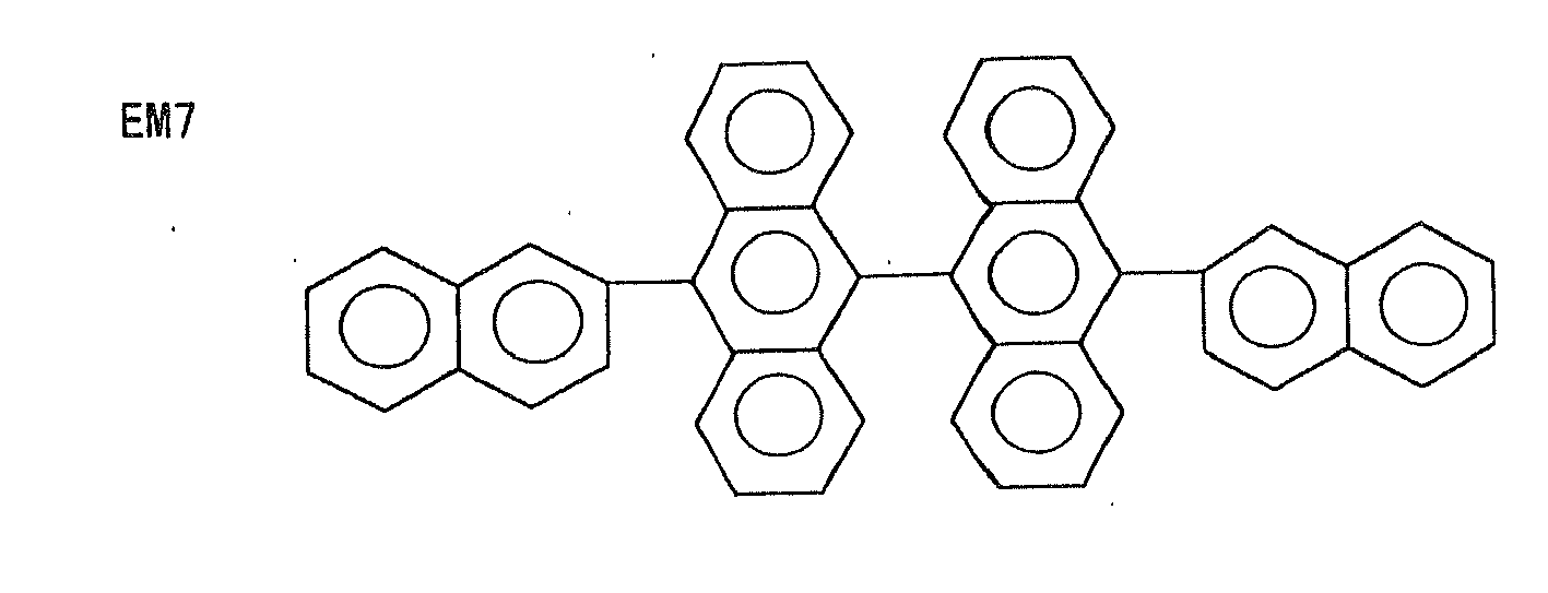


- Specific examples of the anthracene derivative represented by general formula (I-b) are shown in the following.




- Specific examples of the anthracene derivative represented by general formula (II-a) are shown in the following.


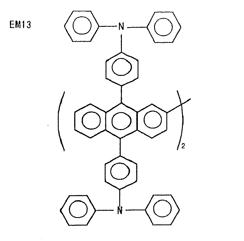
- Specific examples of the styryl derivative containing amine which is represented by general formula (III) are shown in the following.


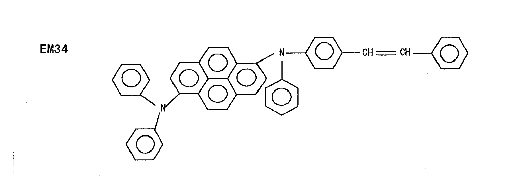

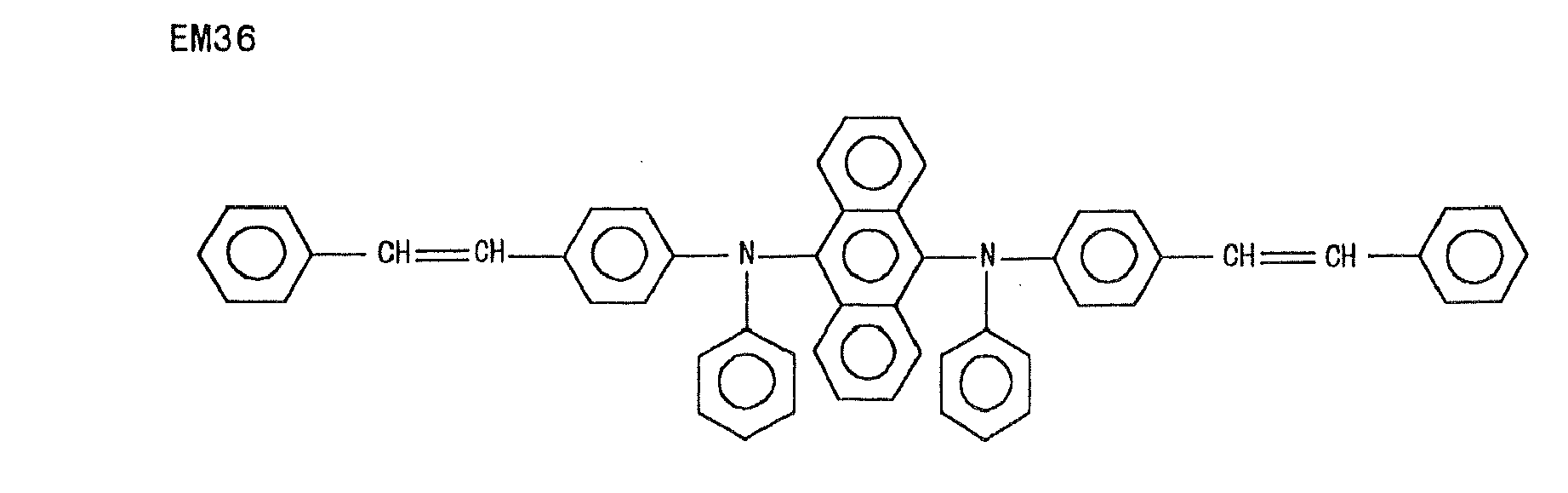


- Specific examples of the styryl derivative containing amine which is represented by general formula (IV) are shown in the following.


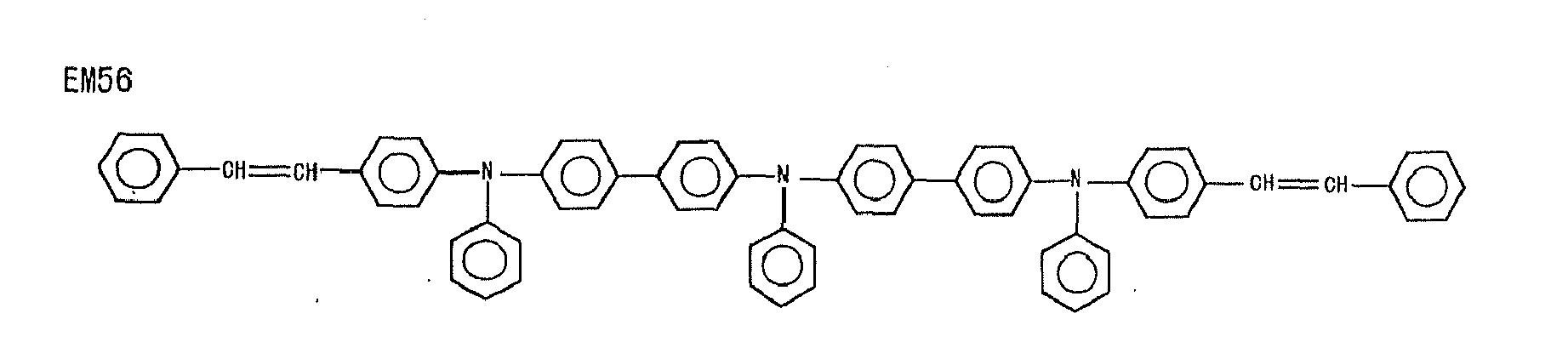


- In the present invention, it is advantageous that the relative amounts of the styryl derivative containing amine of component (A) and the anthracene derivative of component (B) are suitably selected in accordance with the types of the used compounds so that the ratio by weight of component (A) to component (B) is in the range of 1:99 to 99:1. It is particularly preferable that, taking into consideration the fact that the compounds of component (A) have the hole transporting property and the compounds of component (B) have the electron transporting property, the relative amounts are selected so that the life and the efficiency of the obtained device are maximized. The voltage applied to the device can also be decreased by suitably selecting the relative amounts of component (A) and component (B).
- In general, the preferable range of the ratio by weight of component (A) to component (B) is in the range of 2:98 to 9:91 and more preferably in the range of 3:97 to 5:95. A particularly high efficiency can be obtained within the above range. When a decrease in the voltage applied to the device is desired, it is preferable that the ratio by weight of component (A) to component (B) is in the range of 10:90 to 80:20.
- It is preferable that the thickness of the layer of an organic light emitting medium is in the range of 5 to 200 nm. It is more preferable that the thickness is in the range of 10 to 40 nm since the voltage applied to the device can be remarkably decreased.
- Due to the use of the combination of component (A) and component (B) for the layer of an organic light emitting medium, the efficiency can be increased to 3 to 5 times as high as the efficiency obtained by using component (B) alone and the life can be extended at least to 3 times and, when optimized, to 10 times or more as long as the life obtained by using component (B) alone.
- Moreover, due to the use of the combination of component (A) and component (B), the layer of an organic light emitting medium becomes more amorphous and stability is improved. Therefore, more excellent heat resistance is exhibited. As the compound of component (B), a compound having a glass transition temperature of 110°C or higher is preferable. As the compound of component (A), a compound having a glass transition temperature of 70°C or higher is preferable. By using a mixture of the compounds having the above glass transition temperatures, the glass transition temperature of the layer of an organic light emitting medium can be kept at 90°C or higher and a storage durability of 500 hours or longer at 85°C can be obtained.
- The organic EL device comprises a pair of electrodes and a layer of an organic light emitting medium (referred to as a light emitting medium layer, hereinafter) comprising a combination of component (A) and component (B) described above and disposed between the pair of electrodes. It is preferable that various intermediate layers are disposed between the electrodes and the light emitting medium layer. Examples of the intermediate layer include a hole injecting layer, a hole transporting layer, an electron injecting layer and an electron transporting layer. It is known that various organic and inorganic compounds can be used for these layers.
- Typical examples of the construction of the organic EL device include:
- (1) An anode / a light emitting medium layer / a cathode;
- (2) An anode / a hole injecting layer / a light emitting medium layer / a cathode;
- (3) An anode / a light emitting medium layer / an electron injecting layer / a cathode;
- (4) An anode / a hole injecting layer / a light emitting medium layer / an electron injecting layer / a cathode;
- (5) An anode / an organic semiconductor layer / a light emitting medium layer / a cathode;
- (6) An anode / an organic semiconductor layer / an electron barrier layer / a light emitting medium layer / a cathode;
- (7) An anode / an organic semiconductor layer / a light emitting medium layer / an adhesion improving layer / a cathode; and
- (8) An anode / a hole injecting layer / a hole transporting layer / a light emitting medium layer / an electron injecting layer / a cathode.
- In general, the organic EL device is prepared on a substrate which transmits light. The substrate which transmits light is the substrate which supports the organic EL device. It is preferable that the substrate which transmits light has a transmittance of light of 50% or greater in the visible region of 400 to 700 nm. It is also preferable that a flat and smooth substrate is used.
- As the substrate which transmits light, glass plates and synthetic resin plates are advantageously used. Specific examples of the glass plates include plates made of soda ash glass, glass containing barium and strontium, lead glass, aluminosilicate glass, borosilicate glass, barium borosilicate glass and quartz. Specific examples of the synthetic resin plates include plates made of polycarbonate resins, acrylic resins, polyethylene terephthalate resins, polyether sulfide resins and polysulfone resins.
- As the anode, an electrode made of a material such as a metal, an alloy, a conductive compound and a mixture of these materials which has a great work function (4 eV or more) is preferably used. Specific examples of the material for the anode include metals such as Au and conductive materials such as CuI, ITO (indium tin oxide), SnO2, ZnO and In-Zn-O. The anode can be prepared by forming a thin film of the electrode material described above in accordance with a process such as the vapor deposition process and the sputtering process. When the light emitted from the light emitting medium layer is obtained through the anode, it is preferable that the anode has a transmittance of the emitted light greater than 10%. It is also preferable that the sheet resistivity of the anode is several hundred Ω/□ or smaller. The thickness of the anode is, in general, selected in the range of 10 nm to 1 µm and preferably in the range of 10 to 200 nm although the preferable range may be different depending on the used material.
- As the cathode, an electrode made of a material such as a metal, an alloy, a conductive compound and a mixture of these materials which has a small work function (4 eV or smaller) is used. Specific examples of the material for the cathode include sodium, sodium-potassium alloys, magnesium, lithium, magnesium silver mixtures, aluminum/aluminum oxide, Al/Li2O, Al/LiO2, Al/LiF, aluminum-lithium alloys, indium and rare earth metals.
- The cathode can be prepared by forming a thin film of the material described above in accordance with a process such as the vapor deposition process and the sputtering process.
- When the light emitted from the light emitting medium layer is obtained through the cathode, it is preferable that the cathode has a transmittance of the emitted light greater than 10 %. It is also preferable that the sheet resistivity of the cathode is several hundred Ω/□ or smaller. The thickness of the cathode is, in general, selected in the range of 10 nm to 1 µm and preferably in the range of 50 to 200 nm.
- In the organic EL device of the present invention, it is preferable that a layer of a chalcogenide, a metal halide or a metal oxide (this layer may occasionally be referred to as a surface layer) is disposed on the surface of at least one of the pair of electrodes prepared as described above. Specifically, it is preferable that a layer of a chalcogenide (including an oxide) of a metal such as silicon and aluminum is disposed on the surface of the anode at the side of the light emitting medium layer and a layer of a metal halide or a metal oxide is disposed on the surface of the cathode at the side of the light emitting medium layer. Due to the above layers, stability in driving can be improved.
- Preferable examples of the chalcogenide include SiOx (1≦x≦2), AlOx (1≦x≦1.5), SiON and SiAlON. Preferable examples of the metal halide include LiF, MgF2, CaF2 and fluorides of rare earth metals. Preferable examples of the metal oxide include Cs2O, Li2O, MgO, SrO, BaO and CaO.
- In the organic EL device of the present invention, the electron transporting property and the hole transporting property of the light emitting medium layer are simultaneously improved by suitably adjusting the relative amounts of component (A) and component (B) described above and the above intermediate layers such as the hole injecting layer, the hole transporting layer and the electron injecting layer can be omitted. In this case, the surface layers may be disposed. It is preferable that the surface layers are disposed.
- In the organic EL device of the present invention, it is preferable that a mixed region of an electron transmitting compound and a reducing dopant or a mixed region of a hole transmitting compound and a oxidizing dopant is disposed on the surface of at least one of the pair of electrodes prepared as described above. Due to the mixed region disposed on the surface of the pair of electrodes, the electron transmitting compound is reduced to form an anion and injection and transportation of electrons from the mixed region into the light emitting medium can be facilitated. The hole transmitting compound is oxidized to form a cation and injection and transportation of holes from the mixed region into the light emitting medium is facilitated. Preferable examples of the oxidizing dopant include various types of Lewis acid and acceptor compounds. Preferable examples of the reducing dopant include alkali metals, compounds of alkali metals, alkaline earth metals, rare earth metals and compounds of these metals.
- In the organic EL device of the present invention, the light emitting medium layer has the following functions:
- (1) The injecting function: the function of injecting holes from the anode or the hole injecting layer and injecting electrons from the cathode or the electron injecting layer when an electric field is applied;
- (2) The transporting function: the function of transporting injected charges (electrons and holes) by the force of the electric field; and
- (3) The light emitting function: the function of providing the field for recombination of electrons and holes and leading the recombination to the emission of light.
- As the process for forming the light emitting medium layer, a conventional process such as the vapor deposition process, the spin coating process and the LB process can be used. It is particularly preferable that the light emitting medium layer is a molecular deposit film. The molecular deposit film is a thin film formed by deposition of a material compound in the gas phase or a thin film formed by solidification of a material compound in a solution or in the liquid phase. In general, the molecular deposit film can be distinguished from the thin film formed in accordance with the LB process (the molecular accumulation film) based on the differences in the aggregation structure and higher order structures and functional differences caused by these structural differences.
- As disclosed in
Japanese Patent Application Laid-Open No. Show a 57(1982)-51781 - In the present invention, where desired, conventional light emitting media other than component (A) and component (B) described above may be comprised in the light emitting medium layer or a light emitting medium layer comprising other conventional light emitting media may be laminated to the light emitting medium layer comprising the compounds described in the present invention as long as the object of the present invention is not adversely affected.
- The hole injecting and transporting layer is a layer which helps injection of holes into the light emitting medium layer and transports the holes to the light emitting region. The layer exhibits a great mobility of holes and, in general, has an ionization energy as small as 5.5 eV or smaller. For the hole injecting and transporting layer, a material which transports holes to the light emitting medium layer at a smaller electric field strength is preferable. A material which exhibits, for example, a mobility of holes of at least 10-6 cm2/V·sec under application of an electric field of 104 to 106 V/cm is more preferable. A material can be selected from materials which are conventionally used as the charge transporting material of holes in photoconductive materials and conventional materials which are used for the hole injecting layer in organic EL devices and used as the hole injecting and transporting material.
- To form the hole injecting and transporting layer, a thin film may be formed from a hole injecting and transporting material in accordance with a conventional process such as the vacuum vapor deposition process, the spin coating process, the casting process and the LB process. The thickness of the hole injecting and transporting layer is not particularly limited. In general, the thickness is 5 nm to 5 µm.
- The electron injection layer is a layer which helps injection of electrons into the light emitting medium layer and exhibits a great mobility of electrons. The adhesion improving layer is an electron injecting layer made of a material exhibiting excellent adhesion with the cathode. As the material for the electron injecting layer, metal complexes of 8-hydroxyquinoline and derivatives thereof are preferably used. Specific examples of the metal complexes of 8-hydroxyquinoline and derivatives thereof include metal chelates of oxinoid compounds including chelates of oxine (in general, 8-quinolinol or 8-hydroxyquinoline). For example, tris(8-quinolinol)aluminum can be used as the electron injecting material.
- To prepare the organic EL device of the present invention, for example, the anode, the light emitting medium layer and, where necessary, the hole injecting layer and the electron injecting layer are formed in accordance with the above process using the above materials and the cathode is formed in the last step. The organic EL device may be prepared by forming the above layers in the opposite order to that described above, i.e., the cathode being formed in the first step and the anode in the last step.
- An embodiment of the process for preparing an organic EL device having a construction in which an anode, a hole injecting layer, a light emitting medium layer, an electron injecting layer and a cathode are disposed successively on a substrate which transmits light will be described in the following.
- On a suitable substrate which transmits light, a thin film made of a material for the anode is formed in accordance with the vapor deposition process or the sputtering process so that the thickness of the formed thin film is 1 µm or smaller and preferably in the range of 10 to 200 nm. The formed thin film is used as the anode. Then, a hole injecting layer is formed on the anode. The hole injecting layer can be formed in accordance with the vacuum vapor deposition process, the spin coating process, the casting process or the LB process, as described above. The vacuum vapor deposition process is preferable because a uniform film can be easily obtained and the possibility of formation of pin holes is small. When the hole injecting layer is formed in accordance with the vacuum vapor deposition process, in general, it is preferable that the conditions are suitably selected in the following ranges: the temperature of the source of the deposition: 50 to 450°C; the vacuum: 10-7 to 10-3 Torr; the rate of deposition: 0.01 to 50 nm/second; the temperature of the substrate: -50 to 300°C and the thickness of the film: 5 nm to 5 µm; although the conditions of the vacuum vapor deposition are different depending on the used compound (the material for the hole injecting layer) and the crystal structure and the recombination structure of the hole injecting layer to be formed.
- Then, the light emitting medium layer is formed on the hole injecting layer formed above. Using the light emitting medium described in the present invention, a thin film of the organic light emitting medium can be formed in accordance with the vacuum vapor deposition process, the sputtering process, the spin coating process or the casting process and the formed thin film is used as the light emitting medium layer. The vacuum vapor deposition process is preferable because a uniform film can be easily obtained and the possibility of formation of pin holes is small. When the light emitting medium layer is formed in accordance with the vacuum vapor deposition process, in general, the conditions of the vacuum vapor deposition process can be selected in the same ranges as those described for the vacuum vapor deposition of the hole injecting layer although the conditions are different depending on the used compound. It is preferable that the thickness is in the range of 10 to 40 nm.
- An electron injecting layer is formed on the light emitting medium layer formed above. Similarly to the hole injecting layer and the light emitting medium layer, it is preferable that the electron injecting layer is formed in accordance with the vacuum vapor deposition process since a uniform film must be obtained. The conditions of the vacuum vapor deposition can be selected in the same ranges as those described for the vacuum vapor deposition of the hole injecting layer and the light emitting medium layer.
- A cathode is formed on the above layers in the last step and an organic EL device can be obtained. The cathode is made of a metal and can be formed in accordance with the vacuum vapor deposition process or the sputtering process. It is preferable that the vacuum vapor deposition process is used in order to prevent formation of damages on the lower organic layers during the formation of the film.
- In the above preparation of the organic EL device, it is preferable that the above layers from the anode to the cathode are formed successively while the preparation system is kept in a vacuum after being evacuated.
- The electroluminescence device which can be prepared as described above emits light by applying a direct voltage of 3 to 40 V in the condition that the anode is connected to a positive electrode (+) and the cathode is connected to a negative electrode (-). When the connection is reversed, no electric current is observed and no light is emitted at all. When an alternating voltage is applied to the electroluminescence device, light emission is observed only in the condition that the polarity of the anode is positive and the polarity of the cathode is negative. When an alternating voltage is applied to the organic EL device, any type of wave shape can be used.
- The present invention also provides the organic light emitting medium comprising component (A) and component (B) described above. The organic light emitting medium can be advantageously used for the organic EL device which exhibits excellent heat resistance, a long life and a high efficiency and emits bluish light.
- The present invention will be described more specifically with reference to examples in the following. However, the present invention is not limited to the examples.
- In accordance with known processes described in literatures, the following compounds Ant-1, TPD78, TPD107 and PAVB were synthesized and purified.


- On a glass plate having a size of 25×75×1.1 mm, a transparent electrode made of indium tin oxide and having a thickness of 120 nm was formed. After the glass substrate was irradiated with ultraviolet light, exposed to ozone and washed, the glass substrate was placed in a vacuum vapor deposition apparatus.
- In the first step, TPD107 was vapor deposited so that a layer having a thickness of 60 nm was formed and TPD78 was vapor deposited so that a layer having a thickness of 20 nm was formed on the layer of TPD107. Then, Ant-1 and PAVB were simultaneously vapor deposited on the formed layers in amounts such that the ratio by weight of Ant-1 and PAVB was 40:3 and a light emitting medium layer having a thickness of 30 nm was formed.
- Alq (an aluminum complex of 8-hydroxyquinoline) was vapor deposited so that a layer having a thickness of 20 nm was formed on the formed light emitting medium layer. The layers of TPD107, TPD78, Ant-1/PAVB and Alq were the hole injecting layer, the hole transporting layer, the light emitting medium layer and the electron injecting layer, respectively.
- Then, LiF was vapor deposited so that a layer having a thickness of 0.3 nm was formed on the above layers and aluminum was vapor deposited so that a layer having a thickness of 100 nm was formed on the layer of LiF. The layers of LiF and Al worked as the cathode. An organic EL device was prepared as described above.
- The device was tested by passing an electric current. Blue light emission of 110 cd/m2 was obtained at a voltage of 5 V and a current density of 1.05 mA/cm2. The efficiency was 10.4 cd/A.
- The device was tested by continuously passing direct current at a current density of 10 mA/cm2 and the half-life was found to be 1100 hours.
- Organic EL devices were prepared in accordance with the same procedures as those conducted in Example 1 except that the light emitting medium layer was formed from a compound of component (A) and a compound of component (B) shown in Table 1 in amounts shown in Table 1.
- The properties of the obtained organic EL devices are shown in Table 1.
Table 1 - 1 Organic light emitting medium layer Voltage
(V)Current
density (m.A/cm2)component (A) component (B) (A):(B)
(ratio by weight)Example 2 EM43 EM22 3:40 6 4.25 Example 3 EM44 EM22 3:30 6 3.79 Example 4 EM50 EM25 6:30 6 6.25 Example 5 EM51 EM28 8:40 6 7.02 Example 6 EM43 EM2 2:40 6 3.80 Example 7 EM44 EM4 3:20 6 4.90 Example 8 EM50 EM7 4:30 6 5.20 Example 9 EM51 EM9 2:98 6 7.20 Example 10 EM32 EM27 3:40 6 6.20 Example 11 EM36 EM27 3:30 6 7.50 Example 12 EM39 EM27 6:30 6 6.50 Example 13 EM39 EM7 8:40 6 7.48 Example 14 EM44 EM7 2:40 6 4.92 Example 15 EM52 EM7 2:98 6 5.64 Example 16 EM53 EM7 2:40 6 3.82 Table 1 - 2 Luminance Efficiency Half-life under driving at constant current of 10 mA/cm2 (cd/m2) (cd/A) (hour) Example 2 410 9.6 1350 Example 3 390 10.2 1400 Example 4 550 8.8 850 Example 5 620 8.8 1100 Example 6 430 11.3 2100 Example 7 510 10.4 2400 Example 8 490 9.4 1800 Example 9 650 9.0 1300 Example 10 480 7.7 1100 Example 11 650 8.7 920 Example 12 600 9.2 870 Example 13 810 10.8 2200 Example 14 650 13.2 2100 Example 15 600 10.6 1900 Example 16 430 11.3 1400 - A device was prepared in accordance with the same procedures as those conducted in Example 1 except that a mixed layer composed of EM43 and EM2 in amounts such that the ratio by weight of EM43 to EM2 was 3:30 was used as the light emitting medium layer and layers of Alq:Cs and Al were used as the cathode in place of layers of LiF and Al. The layer of Alq:Cs was a layer of a mixture of Alq which was an electron transmitting compound and Cs metal which was a reducing dopant in amounts such that the ratio by mole of Alq to Cs was 1:1. Blue light emission of 120 cd/m2 was obtained at a voltage of 4.5 V and a current density of 1.03 mA/cm2. The light emission could be achieved at a small applied voltage. The efficiency was as high as 11.7 cd/A. The half-life under driving at a constant current of 10 mA/cm2 was 2200 hours.
- An organic EL device was prepared in accordance with the same procedures as those conducted in Example 1 except that EM37 and EM21 were used as component (A) and component (B), respectively, of the light emitting medium layer in amounts such that the ratio by weight of EM37 to EM21 was 2:3. An electric current of 3.25 mA/cm2 was obtained at a voltage of 5 V and blue light was emitted at an efficiency of 4.9 cd/A. The device was tested by continuously passing direct current at a current density of 10 mA/cm2 and the half-life was found to be as long as 3200 hours. The applied voltage could be further decreased by increasing the amount of component (A).
- An organic EL device was prepared in accordance with the same procedures as those conducted in Example 1 except that PAVB which was a styryl derivative containing amine was not vacuum vapor deposited simultaneously.
- The properties of the prepared device was evaluated. A current of 0.8 mA/cm2 was passed at a voltage of 5 V but the luminance was as low as 22 cd/m2. The efficiency was 2.75 cd/A. Therefore, the efficiency obtained in Example 1 was 3.8 times as high as that obtained in Comparative Example 1. The device was tested by continuously passing direct current at a current density of 10 mA/cm2 and the half-life was found to be as short as 200 hours.
- In accordance with the present invention, an organic EL device exhibiting excellent heat resistance, a long life and a high efficiency and emitting blue light can be provided.
- The organic EL device can be advantageously used as the light emitting device in various types of display apparatuses.
Claims (8)
- An anthracene derivative represented by general formula (II):A3 - An - A4 ... (II)wherein An represents 9,10-anthracenylene group,
A3 and A4 each independently represents an unsubstituted α-naphthyl group, an α-naphthyl group substituted by a substituted or unsubstituted monovalent aromatic group having 6 to 40 carbon atoms, or an α-naphthyl group substituted by an amino group substituted by a substituted or unsubstituted aryl group having 5 to 16 carbon atoms and may be the same as or different from each other. - An anthracene derivative described in claim 1, wherein both of A3 and A4 are 4-(α-naphthyl)-α-naphthyl groups and which is represented by the following formula

- An organic electroluminescence device which comprises a pair of electrodes and a layer of an organic light emitting medium, wherein the organic light emitting medium comprises (A) at least one compound selected from the group consisting of monostyryl derivatives containing amine, distyryl derivatives containing amine, tristyryl derivatives containing amine and tetrastyryl derivatives containing amine and (B) at least one compound selected from the group consisting of anthracene derivatives represented by general formula (II):
A3 - An - A4 (II)
wherein An represents 9,10-anthracenylene group,
A3 represents an unsubstituted α-naphthyl group, an α-naphthyl group substituted by a substituted or unsubstituted monovalent aromatic group having 6 to 40 carbon atoms, or an α-naphthyl group substituted by an amino group substituted by an unsubstituted or substituted aryl group having 5 to 16 carbon atoms, and
A4 represents a substituted or unsubstituted monovalent condensed aromatic ring group or a substituted or unsubstituted non-condensed ring based aryl group having 12 or more carbon atoms. - The organic light emitting medium according to claim 3, wherein component (A) is at least one compound selected from the group consisting of styryl derivatives containing amine represented by general formula (III):

styryl derivatives containing amine represented by the general formula (IV) :
- The organic electroluminescence device according to claim 3 or 4, wherein the layer of an organic light emitting medium comprises component (A) and component (B) in amounts such that the ratio by weight of component (A) to component (B) is 2:98 to 9:91.
- The organic electroluminescence device according to any one of claims 3 to 5, wherein a layer of a chalcogenide, a metal halide or a metal oxide is disposed on a surface of at least one of the pair of electrodes.
- An organic electroluminescence device according to any of claims 3 to 6, wherein a mixed region of a reducing dopant and an organic compound or a mixed region of an oxidizing dopant and an organic compound is disposed on a surface of at least one of the pair of electrodes.
- An organic electroluminescence device according to any of claims 3 to 7, wherein the layer of the organic light emitting medium has a thickness of 10 to 400 nm.
Applications Claiming Priority (2)
| Application Number | Priority Date | Filing Date | Title |
|---|---|---|---|
| JP26746099 | 1999-09-21 | ||
| EP00961101A EP1167488B1 (en) | 1999-09-21 | 2000-09-20 | Organic electroluminescent device and organic luminous medium |
Related Parent Applications (1)
| Application Number | Title | Priority Date | Filing Date |
|---|---|---|---|
| EP00961101A Division EP1167488B1 (en) | 1999-09-21 | 2000-09-20 | Organic electroluminescent device and organic luminous medium |
Publications (2)
| Publication Number | Publication Date |
|---|---|
| EP1775783A2 true EP1775783A2 (en) | 2007-04-18 |
| EP1775783A3 EP1775783A3 (en) | 2008-04-16 |
Family
ID=17445157
Family Applications (2)
| Application Number | Title | Priority Date | Filing Date |
|---|---|---|---|
| EP00961101A Revoked EP1167488B1 (en) | 1999-09-21 | 2000-09-20 | Organic electroluminescent device and organic luminous medium |
| EP07101123A Ceased EP1775783A3 (en) | 1999-09-21 | 2000-09-20 | Organic electroluminescence device and organic light emitting medium |
Family Applications Before (1)
| Application Number | Title | Priority Date | Filing Date |
|---|---|---|---|
| EP00961101A Revoked EP1167488B1 (en) | 1999-09-21 | 2000-09-20 | Organic electroluminescent device and organic luminous medium |
Country Status (9)
| Country | Link |
|---|---|
| US (1) | US6534199B1 (en) |
| EP (2) | EP1167488B1 (en) |
| JP (1) | JP5073899B2 (en) |
| KR (4) | KR100809132B1 (en) |
| CN (1) | CN1208422C (en) |
| AT (1) | ATE360892T1 (en) |
| DE (1) | DE60034560T2 (en) |
| TW (1) | TW474113B (en) |
| WO (1) | WO2001021729A1 (en) |
Families Citing this family (156)
| Publication number | Priority date | Publication date | Assignee | Title |
|---|---|---|---|---|
| EP2270117A3 (en) * | 1998-12-28 | 2011-04-27 | Idemitsu Kosan Co., Ltd. | Organic electroluminescence device |
| KR100721656B1 (en) * | 2005-11-01 | 2007-05-23 | 주식회사 엘지화학 | Organic electrical devices |
| WO2002014244A1 (en) * | 2000-08-10 | 2002-02-21 | Mitsui Chemicals, Inc. | Hydrocarbon compound, material for organic electroluminescent element and organic electroluminescent element |
| JP4838969B2 (en) * | 2000-09-01 | 2011-12-14 | 出光興産株式会社 | Novel styryl compound and organic electroluminescence device |
| JP4220669B2 (en) * | 2000-12-26 | 2009-02-04 | 出光興産株式会社 | Organic electroluminescence device |
| JP4046267B2 (en) * | 2002-03-26 | 2008-02-13 | 株式会社半導体エネルギー研究所 | Display device |
| JP4646494B2 (en) * | 2002-04-11 | 2011-03-09 | 出光興産株式会社 | Novel nitrogen-containing heterocyclic derivative and organic electroluminescence device using the same |
| JP4161262B2 (en) * | 2002-06-26 | 2008-10-08 | ソニー株式会社 | ORGANIC ELECTROLUMINESCENT ELEMENT AND LIGHT EMITTING OR DISPLAY DEVICE USING THE SAME |
| EP1541657B2 (en) | 2002-07-19 | 2014-03-05 | Idemitsu Kosan Co., Ltd. | Organic electroluminescent devices and organic luminescent medium |
| JP4025137B2 (en) * | 2002-08-02 | 2007-12-19 | 出光興産株式会社 | Anthracene derivative and organic electroluminescence device using the same |
| WO2004018587A1 (en) * | 2002-08-23 | 2004-03-04 | Idemitsu Kosan Co., Ltd. | Organic electroluminescence device and anthracene derivative |
| JP4287198B2 (en) * | 2002-11-18 | 2009-07-01 | 出光興産株式会社 | Organic electroluminescence device |
| CN100518424C (en) * | 2002-11-18 | 2009-07-22 | 出光兴产株式会社 | organic electroluminescent element |
| EP1437395B2 (en) † | 2002-12-24 | 2015-08-26 | LG Display Co., Ltd. | Organic electroluminescent device |
| KR100624407B1 (en) * | 2003-01-02 | 2006-09-18 | 삼성에스디아이 주식회사 | Diphenylanthracene derivative and organic electroluminescent device employing the same |
| WO2004063159A1 (en) * | 2003-01-10 | 2004-07-29 | Idemitsu Kosan Co., Ltd. | Nitrogenous heterocyclic derivative and organic electroluminescent element employing the same |
| JPWO2004074399A1 (en) * | 2003-02-20 | 2006-06-01 | 出光興産株式会社 | Material for organic electroluminescence device and organic electroluminescence device using the same |
| US7651788B2 (en) * | 2003-03-05 | 2010-01-26 | Lg Display Co., Ltd. | Organic electroluminescent device |
| JP4624653B2 (en) * | 2003-05-20 | 2011-02-02 | 出光興産株式会社 | Organic electroluminescence element and display device |
| JP3840235B2 (en) * | 2003-06-27 | 2006-11-01 | キヤノン株式会社 | Organic light emitting device |
| US20050079383A1 (en) * | 2003-10-14 | 2005-04-14 | Lightronik Technology Inc. | Organic light emitting medium containing 9, 9' -bianthry-10,10' -phenanthrcene and device containing the medium |
| EP1696015B1 (en) | 2003-12-19 | 2015-05-13 | Idemitsu Kosan Co., Ltd. | Light-emitting material for organic electroluminescent device, organic electroluminescent device using same, and material for organic electroluminescent device |
| US20070103055A1 (en) * | 2003-12-19 | 2007-05-10 | Idemitsu Losan Co., Ltd. | Organic electroluminescence device, conductive laminate and display |
| KR100577262B1 (en) | 2004-01-06 | 2006-05-10 | 엘지전자 주식회사 | Organic light emitting diode |
| US9085729B2 (en) * | 2004-02-09 | 2015-07-21 | Lg Display Co., Ltd. | Blue emitters for use in organic electroluminescence devices |
| US7252893B2 (en) * | 2004-02-17 | 2007-08-07 | Eastman Kodak Company | Anthracene derivative host having ranges of dopants |
| WO2005081587A1 (en) * | 2004-02-19 | 2005-09-01 | Idemitsu Kosan Co., Ltd. | White color organic electroluminescence device |
| JPWO2005091686A1 (en) * | 2004-03-19 | 2008-02-07 | チッソ株式会社 | Organic electroluminescence device |
| JP4734836B2 (en) * | 2004-03-19 | 2011-07-27 | 富士ゼロックス株式会社 | Electroluminescent device |
| WO2005091684A1 (en) * | 2004-03-19 | 2005-09-29 | Idemitsu Kosan Co., Ltd. | Organic electroluminescent device |
| JP2005302667A (en) * | 2004-04-15 | 2005-10-27 | Idemitsu Kosan Co Ltd | Organic electroluminescence device |
| JP4705914B2 (en) * | 2004-05-27 | 2011-06-22 | 出光興産株式会社 | Asymmetric pyrene derivative and organic electroluminescence device using the same |
| TWI290582B (en) * | 2004-07-06 | 2007-12-01 | Au Optronics Corp | Anthracene compound and organic electroluminescent device including the anthracene compound |
| JP4788202B2 (en) * | 2004-07-09 | 2011-10-05 | Jnc株式会社 | Luminescent material and organic electroluminescent device using the same |
| US20060019116A1 (en) * | 2004-07-22 | 2006-01-26 | Eastman Kodak Company | White electroluminescent device with anthracene derivative host |
| US7449831B2 (en) | 2004-08-02 | 2008-11-11 | Lg Display Co., Ltd. | OLEDs having inorganic material containing anode capping layer |
| US7449830B2 (en) | 2004-08-02 | 2008-11-11 | Lg Display Co., Ltd. | OLEDs having improved luminance stability |
| US7666524B2 (en) * | 2004-10-29 | 2010-02-23 | Semiconductor Energy Laboratory Co., Ltd. | Oligonaphthalene derivatives, and light-emitting element and light-emitting device using oligonaphthalene derivatives |
| US7544425B2 (en) * | 2004-10-29 | 2009-06-09 | Eastman Kodak Company | Organic element for electroluminescent devices |
| WO2006049316A1 (en) * | 2004-11-08 | 2006-05-11 | Bando Chemical Industries, Ltd. | Novel aromatic tertiary amines and utilization thereof as organic electronic functional material |
| US20080207823A1 (en) * | 2004-12-29 | 2008-08-28 | E.I. Du Pont De Nemours And Company | Active Compositions And Methods |
| US8057916B2 (en) * | 2005-04-20 | 2011-11-15 | Global Oled Technology, Llc. | OLED device with improved performance |
| US20060240281A1 (en) * | 2005-04-21 | 2006-10-26 | Eastman Kodak Company | Contaminant-scavenging layer on OLED anodes |
| TWI268121B (en) | 2005-04-21 | 2006-12-01 | Au Optronics Corp | Light emission material and organic electroluminescent device using the same |
| US7777407B2 (en) | 2005-05-04 | 2010-08-17 | Lg Display Co., Ltd. | Organic light emitting devices comprising a doped triazine electron transport layer |
| US8487527B2 (en) | 2005-05-04 | 2013-07-16 | Lg Display Co., Ltd. | Organic light emitting devices |
| US7811679B2 (en) | 2005-05-20 | 2010-10-12 | Lg Display Co., Ltd. | Display devices with light absorbing metal nanoparticle layers |
| US7943244B2 (en) | 2005-05-20 | 2011-05-17 | Lg Display Co., Ltd. | Display device with metal-organic mixed layer anodes |
| US7795806B2 (en) | 2005-05-20 | 2010-09-14 | Lg Display Co., Ltd. | Reduced reflectance display devices containing a thin-layer metal-organic mixed layer (MOML) |
| US7750561B2 (en) | 2005-05-20 | 2010-07-06 | Lg Display Co., Ltd. | Stacked OLED structure |
| US7728517B2 (en) | 2005-05-20 | 2010-06-01 | Lg Display Co., Ltd. | Intermediate electrodes for stacked OLEDs |
| KR100788254B1 (en) * | 2005-08-16 | 2007-12-27 | (주)그라쎌 | Green electroluminescent compounds and organic electroluminescent device using the same |
| DE102005040411A1 (en) | 2005-08-26 | 2007-03-01 | Merck Patent Gmbh | New materials for organic electroluminescent devices |
| US20070048545A1 (en) * | 2005-08-31 | 2007-03-01 | Eastman Kodak Company | Electron-transporting layer for white OLED device |
| KR101359412B1 (en) | 2005-08-31 | 2014-02-27 | 가부시키가이샤 한도오따이 에네루기 켄큐쇼 | Carbazole derivative, Material for light emitting element, Light emitting element, Light emitting device, and Electronic device |
| US20070092754A1 (en) * | 2005-10-26 | 2007-04-26 | Eastman Kodak Company | Organic element for low voltage electroluminescent devices |
| KR100828173B1 (en) * | 2005-11-22 | 2008-05-08 | (주)그라쎌 | Organic Electroluminescent Compounds and Display Device using The Same |
| DE102005058557A1 (en) * | 2005-12-08 | 2007-06-14 | Merck Patent Gmbh | Organic electroluminescent device |
| WO2007065550A1 (en) * | 2005-12-08 | 2007-06-14 | Merck Patent Gmbh | Novel materials for organic electroluminescent devices |
| DE102005058558A1 (en) * | 2005-12-08 | 2007-06-14 | Merck Patent Gmbh | Organic electroluminescent devices |
| KR100851739B1 (en) | 2006-01-13 | 2008-08-11 | 주식회사 엘지화학 | Light emitting material and organic light emitting device using same |
| TWI371987B (en) * | 2006-01-18 | 2012-09-01 | Lg Chemical Ltd | Oled having stacked organic light-emitting units |
| KR100670383B1 (en) | 2006-01-18 | 2007-01-16 | 삼성에스디아이 주식회사 | Organic light emitting device and flat panel display device having the same |
| TWI348463B (en) * | 2006-03-06 | 2011-09-11 | Lg Chemical Ltd | Novel anthracene derivative and organic electronic device using the same |
| KR100667973B1 (en) * | 2006-03-09 | 2007-01-11 | 주식회사 잉크테크 | Novel distyrylarylene compounds and organic electroluminescent devices using the same |
| DE102006013802A1 (en) | 2006-03-24 | 2007-09-27 | Merck Patent Gmbh | New materials for organic electroluminescent devices |
| EP2355198B1 (en) | 2006-05-08 | 2015-09-09 | Global OLED Technology LLC | OLED electron-injecting layer |
| DE102006031990A1 (en) | 2006-07-11 | 2008-01-17 | Merck Patent Gmbh | New materials for organic electroluminescent devices |
| US7667391B2 (en) * | 2006-08-04 | 2010-02-23 | Eastman Kodak Company | Electrically excited organic light-emitting diodes with spatial and spectral coherence |
| KR100864308B1 (en) * | 2006-12-28 | 2008-10-20 | 주식회사 두산 | Novel anthracene derivatives and organic electroluminescent devices using them |
| DE102007024850A1 (en) | 2007-05-29 | 2008-12-04 | Merck Patent Gmbh | New materials for organic electroluminescent devices |
| US20090091242A1 (en) * | 2007-10-05 | 2009-04-09 | Liang-Sheng Liao | Hole-injecting layer in oleds |
| KR100935356B1 (en) * | 2007-11-19 | 2010-01-06 | 다우어드밴스드디스플레이머티리얼 유한회사 | Green light emitting compound and organic electroluminescent device employing the same as light emitting material |
| JP5399920B2 (en) * | 2007-11-21 | 2014-01-29 | 出光興産株式会社 | Condensed aromatic derivative and organic electroluminescence device using the same |
| US20110054229A1 (en) * | 2007-11-23 | 2011-03-03 | Gracel Display Inc. | Luminescent compounds and electroluminescent device using the same |
| KR100940938B1 (en) * | 2007-12-04 | 2010-02-08 | 다우어드밴스드디스플레이머티리얼 유한회사 | Novel organic light emitting compound and organic electroluminescent device employing it as light emitting material |
| KR100974562B1 (en) * | 2007-12-31 | 2010-08-06 | 다우어드밴스드디스플레이머티리얼 유한회사 | Novel organic light emitting compound and organic light emitting device employing the same as light emitting material |
| KR100991416B1 (en) * | 2007-12-31 | 2010-11-03 | 다우어드밴스드디스플레이머티리얼 유한회사 | Organic light emitting compound and organic light emitting device comprising the same |
| DE102008008953B4 (en) * | 2008-02-13 | 2019-05-09 | Merck Patent Gmbh | New materials for organic electroluminescent devices |
| US8115399B2 (en) * | 2008-02-19 | 2012-02-14 | General Electric Company | OLED light source |
| KR101001384B1 (en) * | 2008-02-29 | 2010-12-14 | 다우어드밴스드디스플레이머티리얼 유한회사 | Novel organic light emitting compound and organic electroluminescent device employing it as light emitting material |
| KR100864303B1 (en) * | 2008-03-05 | 2008-10-20 | 주식회사 두산 | Novel anthracene derivatives and organic electroluminescent devices using them |
| KR100901887B1 (en) * | 2008-03-14 | 2009-06-09 | (주)그라쎌 | Novel organic light emitting compound and organic light emitting device employing the same |
| KR100989815B1 (en) * | 2008-03-20 | 2010-10-29 | 다우어드밴스드디스플레이머티리얼 유한회사 | Novel organic light emitting compound and organic light emitting device employing the same as light emitting material |
| KR100946411B1 (en) | 2008-03-28 | 2010-03-09 | 다우어드밴스드디스플레이머티리얼 유한회사 | Novel organic light emitting compound and organic light emitting device employing the same as light emitting material |
| KR20090105495A (en) * | 2008-04-02 | 2009-10-07 | (주)그라쎌 | Novel organic light emitting compound and organic electroluminescent device employing it as light emitting material |
| KR100910150B1 (en) * | 2008-04-02 | 2009-08-03 | (주)그라쎌 | Novel organic light emitting compound and organic light emitting device employing the same as light emitting material |
| DE102008018670A1 (en) | 2008-04-14 | 2009-10-15 | Merck Patent Gmbh | New materials for organic electroluminescent devices |
| KR101495547B1 (en) | 2008-04-17 | 2015-02-25 | 롬엔드하스전자재료코리아유한회사 | Novel compounds for electronic material and organic electronic device using the same |
| KR20090111915A (en) * | 2008-04-23 | 2009-10-28 | (주)그라쎌 | Novel organic light emitting compound and organic light emitting device employing the same as light emitting material |
| KR20100000772A (en) * | 2008-06-25 | 2010-01-06 | 다우어드밴스드디스플레이머티리얼 유한회사 | Novel organic electroluminescent compounds and organic electroluminescent device using the same |
| EP2145936A3 (en) * | 2008-07-14 | 2010-03-17 | Gracel Display Inc. | Fluorene and pyrene derivatives and organic electroluminescent device using the same |
| KR20100041043A (en) * | 2008-10-13 | 2010-04-22 | 다우어드밴스드디스플레이머티리얼 유한회사 | Novel organic electroluminescent compounds and organic electroluminescent device using the same |
| DE102008054141A1 (en) | 2008-10-31 | 2010-05-06 | Merck Patent Gmbh | New materials for organic electroluminescent devices |
| DE102009005746A1 (en) | 2009-01-23 | 2010-07-29 | Merck Patent Gmbh | Materials for organic electroluminescent devices |
| US8147989B2 (en) * | 2009-02-27 | 2012-04-03 | Global Oled Technology Llc | OLED device with stabilized green light-emitting layer |
| DE102009033371A1 (en) | 2009-07-16 | 2011-05-12 | Merck Patent Gmbh | Materials for electronic devices |
| DE102009034625A1 (en) | 2009-07-27 | 2011-02-03 | Merck Patent Gmbh | New materials for organic electroluminescent devices |
| US8581262B2 (en) | 2009-08-04 | 2013-11-12 | Merck Patent Gmbh | Electronic devices comprising multi cyclic hydrocarbons |
| DE102009051172A1 (en) | 2009-10-29 | 2011-05-05 | Merck Patent Gmbh | Materials for electronic devices |
| DE102009053191A1 (en) | 2009-11-06 | 2011-05-12 | Merck Patent Gmbh | Materials for electronic devices |
| DE102009052428A1 (en) | 2009-11-10 | 2011-05-12 | Merck Patent Gmbh | Connection for electronic devices |
| US8242489B2 (en) * | 2009-12-17 | 2012-08-14 | Global Oled Technology, Llc. | OLED with high efficiency blue light-emitting layer |
| EP2517537B1 (en) | 2009-12-22 | 2019-04-03 | Merck Patent GmbH | Electroluminescent functional surfactants |
| WO2011076314A1 (en) | 2009-12-22 | 2011-06-30 | Merck Patent Gmbh | Electroluminescent formulations |
| JP5836970B2 (en) | 2009-12-22 | 2015-12-24 | メルク パテント ゲーエムベーハー | Formulations containing functional materials |
| DE102010005697A1 (en) | 2010-01-25 | 2011-07-28 | Merck Patent GmbH, 64293 | Connections for electronic devices |
| WO2011110277A1 (en) | 2010-03-11 | 2011-09-15 | Merck Patent Gmbh | Fibers in therapy and cosmetics |
| JP2013522816A (en) | 2010-03-11 | 2013-06-13 | メルク パテント ゲーエムベーハー | Light emitting fiber |
| KR101191644B1 (en) | 2010-05-18 | 2012-10-17 | 삼성디스플레이 주식회사 | Organic Materials and Organic Light Emitting Devices Using the Same |
| JP5944380B2 (en) | 2010-05-27 | 2016-07-05 | メルク パテント ゲーエムベーハー | Composition comprising quantum dots |
| CN103026525B (en) | 2010-07-26 | 2016-11-09 | 默克专利有限公司 | Nanocrystals in Devices |
| DE102010048074A1 (en) | 2010-10-09 | 2012-04-12 | Merck Patent Gmbh | Materials for electronic devices |
| DE102010054316A1 (en) | 2010-12-13 | 2012-06-14 | Merck Patent Gmbh | Substituted tetraarylbenzenes |
| CN102533092A (en) * | 2010-12-30 | 2012-07-04 | 拜耳材料科技(中国)有限公司 | Polyurethane coating film-forming material, polyurethane coating and application thereof |
| DE102011011104A1 (en) | 2011-02-12 | 2012-08-16 | Merck Patent Gmbh | Substituted dibenzonaphthacenes |
| JP6351974B2 (en) | 2011-02-14 | 2018-07-04 | メルク パテント ゲーエムベーハー | Devices and methods for treatment of cells and cellular tissues |
| WO2012126566A1 (en) | 2011-03-24 | 2012-09-27 | Merck Patent Gmbh | Organic ionic functional materials |
| EP2707911B1 (en) | 2011-05-12 | 2017-07-05 | Merck Patent GmbH | Compositions and electronic devices |
| WO2013013754A1 (en) | 2011-07-25 | 2013-01-31 | Merck Patent Gmbh | Copolymers with functionalized side chains |
| JP6282114B2 (en) * | 2011-10-04 | 2018-02-21 | 株式会社Joled | Organic electroluminescence device |
| KR102126877B1 (en) | 2012-02-03 | 2020-06-25 | 이데미쓰 고산 가부시키가이샤 | Carbazole compound, organic electroluminescent material, and organic electroluminescent element |
| CN103456897B (en) * | 2012-05-30 | 2016-03-09 | 京东方科技集团股份有限公司 | Organic electroluminescence device |
| CN103450883B (en) * | 2012-05-30 | 2016-03-02 | 京东方科技集团股份有限公司 | Organic electronic material |
| US20160163987A1 (en) | 2013-07-29 | 2016-06-09 | Merck Patent Gmbh | Electro-optical device and the use thereof |
| WO2015014429A1 (en) | 2013-07-29 | 2015-02-05 | Merck Patent Gmbh | Electroluminescence device |
| KR102717935B1 (en) | 2013-07-30 | 2024-10-16 | 메르크 파텐트 게엠베하 | Materials for electronic devices |
| KR102202756B1 (en) | 2013-07-30 | 2021-01-13 | 메르크 파텐트 게엠베하 | Materials for electronic devices |
| CN103664495B (en) * | 2013-12-10 | 2016-07-06 | 京东方科技集团股份有限公司 | Anthracene derivative and preparation method, application and organic luminescent device |
| CN106255687B (en) | 2014-04-30 | 2020-06-05 | 默克专利有限公司 | Material for electronic devices |
| DE102014008722B4 (en) | 2014-06-18 | 2024-08-22 | Merck Patent Gmbh | Compositions for electronic devices, formulation containing them, use of the composition, use of the formulation and organic electronic device containing the composition |
| KR102385227B1 (en) * | 2014-12-02 | 2022-04-12 | 삼성디스플레이 주식회사 | Compound and organic light emitting device comprising same |
| CN107004777B (en) | 2014-12-04 | 2019-03-26 | 广州华睿光电材料有限公司 | Polymers, mixtures, compositions, organic electronic devices containing the same, and monomers thereof |
| CN107406384B (en) | 2014-12-04 | 2021-07-23 | 广州华睿光电材料有限公司 | Deuterated organic compounds, mixtures, compositions and organic electronic devices comprising the same |
| CN107004779B (en) | 2014-12-11 | 2019-03-08 | 广州华睿光电材料有限公司 | Organic compounds, mixtures containing the same, compositions and organic electronic devices |
| WO2016091217A1 (en) | 2014-12-11 | 2016-06-16 | 广州华睿光电材料有限公司 | Organic metal complex, and polymer, mixture, composition and organic electronic device containing same and use thereof |
| WO2017080326A1 (en) | 2015-11-12 | 2017-05-18 | 广州华睿光电材料有限公司 | Printing composition, electronic device comprising same and preparation method for functional material thin film |
| WO2018095382A1 (en) | 2016-11-23 | 2018-05-31 | 广州华睿光电材料有限公司 | Aromatic amine derivative, preparation method therefor, and uses thereof |
| WO2018095395A1 (en) | 2016-11-23 | 2018-05-31 | 广州华睿光电材料有限公司 | High polymer, mixture containing same, composition, organic electronic component, and monomer for polymerization |
| WO2018095389A1 (en) | 2016-11-23 | 2018-05-31 | 广州华睿光电材料有限公司 | Nitrogen-containing fused heterocyclic ring compound and application thereof |
| WO2018095385A1 (en) | 2016-11-23 | 2018-05-31 | 广州华睿光电材料有限公司 | Fused ring compound, high polymer, mixture, composition, and organic electronic component |
| WO2018095381A1 (en) | 2016-11-23 | 2018-05-31 | 广州华睿光电材料有限公司 | Printing ink composition, preparation method therefor, and uses thereof |
| EP3547385B1 (en) | 2016-11-23 | 2020-11-04 | Guangzhou Chinaray Optoelectronic Materials Ltd. | Organic mixture, composition, and organic electronic component |
| WO2018095379A1 (en) | 2016-11-23 | 2018-05-31 | 广州华睿光电材料有限公司 | Metal organic complex, high polymer, composition, and organic electronic component |
| CN109790129B (en) | 2016-12-08 | 2022-08-12 | 广州华睿光电材料有限公司 | Pyrenetriazine Derivatives and Their Applications in Organic Electronic Devices |
| CN109790118A (en) | 2016-12-13 | 2019-05-21 | 广州华睿光电材料有限公司 | Conjugated polymer and its application in organic electronic device |
| CN109792003B (en) | 2016-12-22 | 2020-10-16 | 广州华睿光电材料有限公司 | Diels-Alder Reaction-Based Crosslinkable Polymers and Their Applications in Organic Electronic Devices |
| CN109790136B (en) | 2016-12-22 | 2024-01-12 | 广州华睿光电材料有限公司 | Furan cross-linking group-containing polymer and application thereof |
| WO2018150832A1 (en) * | 2017-02-16 | 2018-08-23 | 学校法人関西学院 | Organic electroluminescence element |
| US11778907B2 (en) | 2017-04-13 | 2023-10-03 | Merck Patent Gmbh | Composition for organic electronic devices |
| JP7325731B2 (en) | 2018-08-23 | 2023-08-15 | 国立大学法人九州大学 | organic electroluminescence element |
| EP4139971A1 (en) | 2020-04-21 | 2023-03-01 | Merck Patent GmbH | Emulsions comprising organic functional materials |
| CN116391006B (en) | 2020-10-14 | 2025-08-26 | 浙江光昊光电科技有限公司 | Composition and its application in optoelectronic field |
| CN116391007A (en) | 2020-10-14 | 2023-07-04 | 浙江光昊光电科技有限公司 | Organic Compounds and Their Applications in Optoelectronics |
| KR20240045247A (en) | 2021-08-02 | 2024-04-05 | 메르크 파텐트 게엠베하 | Printing method by combining inks |
| TW202411366A (en) | 2022-06-07 | 2024-03-16 | 德商麥克專利有限公司 | Method of printing a functional layer of an electronic device by combining inks |
Family Cites Families (16)
| Publication number | Priority date | Publication date | Assignee | Title |
|---|---|---|---|---|
| JPH01174097A (en) * | 1987-12-28 | 1989-07-10 | Toshiba Corp | Process monitor control system |
| JPH01174079A (en) * | 1987-12-28 | 1989-07-10 | Hitachi Ltd | Picture processing circuit |
| US5536949A (en) * | 1992-08-28 | 1996-07-16 | Idemistu Kosan Co., Ltd. | Charge injection auxiliary material and organic electroluminescence device containing the same |
| US5652067A (en) * | 1992-09-10 | 1997-07-29 | Toppan Printing Co., Ltd. | Organic electroluminescent device |
| DE69511755T2 (en) | 1994-04-26 | 2000-01-13 | Tdk Corp | Phenylanthracene derivative and organic EL element |
| JP3529543B2 (en) * | 1995-04-27 | 2004-05-24 | パイオニア株式会社 | Organic electroluminescence device |
| US5981092A (en) * | 1996-03-25 | 1999-11-09 | Tdk Corporation | Organic El device |
| JP3564859B2 (en) | 1996-04-01 | 2004-09-15 | 東洋インキ製造株式会社 | Organic electroluminescent device material and organic electroluminescent device using the same |
| EP1211301A1 (en) * | 1996-10-08 | 2002-06-05 | Idemitsu Kosan Co., Ltd. | Organic electroluminescent device |
| JP3228502B2 (en) * | 1996-10-08 | 2001-11-12 | 出光興産株式会社 | Organic electroluminescence device |
| JP3949214B2 (en) * | 1997-03-18 | 2007-07-25 | 出光興産株式会社 | Organic electroluminescence device |
| JPH1174079A (en) | 1997-06-20 | 1999-03-16 | Nec Corp | Organic electroluminescence device |
| US5935721A (en) * | 1998-03-20 | 1999-08-10 | Eastman Kodak Company | Organic electroluminescent elements for stable electroluminescent |
| US6140763A (en) * | 1998-07-28 | 2000-10-31 | Eastman Kodak Company | Interfacial electron-injecting layer formed from a doped cathode for organic light-emitting structure |
| JP2000164363A (en) * | 1998-11-25 | 2000-06-16 | Idemitsu Kosan Co Ltd | Organic electroluminescence device |
| JP2001052870A (en) * | 1999-06-03 | 2001-02-23 | Tdk Corp | Organic EL device |
-
2000
- 2000-09-20 WO PCT/JP2000/006402 patent/WO2001021729A1/en not_active Ceased
- 2000-09-20 EP EP00961101A patent/EP1167488B1/en not_active Revoked
- 2000-09-20 KR KR1020017006271A patent/KR100809132B1/en not_active Expired - Lifetime
- 2000-09-20 KR KR1020077019127A patent/KR100790663B1/en not_active Ceased
- 2000-09-20 JP JP2001525292A patent/JP5073899B2/en not_active Expired - Fee Related
- 2000-09-20 CN CNB008020027A patent/CN1208422C/en not_active Expired - Lifetime
- 2000-09-20 KR KR1020057017620A patent/KR100738762B1/en not_active Expired - Fee Related
- 2000-09-20 KR KR1020077006875A patent/KR100799799B1/en not_active Expired - Fee Related
- 2000-09-20 US US09/665,416 patent/US6534199B1/en not_active Expired - Lifetime
- 2000-09-20 TW TW089119391A patent/TW474113B/en not_active IP Right Cessation
- 2000-09-20 AT AT00961101T patent/ATE360892T1/en not_active IP Right Cessation
- 2000-09-20 DE DE60034560T patent/DE60034560T2/en not_active Expired - Lifetime
- 2000-09-20 EP EP07101123A patent/EP1775783A3/en not_active Ceased
Also Published As
| Publication number | Publication date |
|---|---|
| EP1167488B1 (en) | 2007-04-25 |
| DE60034560T2 (en) | 2007-08-16 |
| DE60034560D1 (en) | 2007-06-06 |
| JP5073899B2 (en) | 2012-11-14 |
| US6534199B1 (en) | 2003-03-18 |
| KR20070042584A (en) | 2007-04-23 |
| KR100799799B1 (en) | 2008-02-01 |
| ATE360892T1 (en) | 2007-05-15 |
| CN1322232A (en) | 2001-11-14 |
| EP1167488A1 (en) | 2002-01-02 |
| TW474113B (en) | 2002-01-21 |
| KR100809132B1 (en) | 2008-02-29 |
| EP1167488A4 (en) | 2005-09-07 |
| EP1775783A3 (en) | 2008-04-16 |
| KR20070091375A (en) | 2007-09-10 |
| KR20010080488A (en) | 2001-08-22 |
| KR100738762B1 (en) | 2007-07-12 |
| CN1208422C (en) | 2005-06-29 |
| KR100790663B1 (en) | 2008-01-03 |
| KR20050100708A (en) | 2005-10-19 |
| WO2001021729A1 (en) | 2001-03-29 |
Similar Documents
| Publication | Publication Date | Title |
|---|---|---|
| EP1167488B1 (en) | Organic electroluminescent device and organic luminous medium | |
| US6713192B2 (en) | Organic electroluminescence device and organic light emitting medium | |
| EP1541657B2 (en) | Organic electroluminescent devices and organic luminescent medium | |
| EP2270897B1 (en) | Electroluminescent device with anthracene derivatives in the hole transport layer | |
| JPWO2001021729A1 (en) | Organic electroluminescent device and organic light-emitting medium | |
| US7429425B2 (en) | Oligoarylene derivatives and organic electroluminescent devices made by using the same | |
| US6646164B2 (en) | Triphenylamine derivative and organic electroluminescence device comprising the same | |
| KR20050022870A (en) | Fluorescent material, organic electroluminescent element and organic electroluminescent display | |
| JP2006287248A (en) | Organic electroluminescence device and organic light emitting medium |
Legal Events
| Date | Code | Title | Description |
|---|---|---|---|
| PUAI | Public reference made under article 153(3) epc to a published international application that has entered the european phase |
Free format text: ORIGINAL CODE: 0009012 |
|
| AC | Divisional application: reference to earlier application |
Ref document number: 1167488 Country of ref document: EP Kind code of ref document: P |
|
| AK | Designated contracting states |
Kind code of ref document: A2 Designated state(s): AT BE CH CY DE DK ES FI FR GB GR IE IT LI LU MC NL PT SE |
|
| RIN1 | Information on inventor provided before grant (corrected) |
Inventor name: IKEDA, HIDETSUGU Inventor name: HIGASHI, HISAHIRO,C/O IDEMITSU KOSAN CO., LTD. Inventor name: FUKUOKA, KENICHI Inventor name: HOSOKAWA, CHISHIO |
|
| PUAL | Search report despatched |
Free format text: ORIGINAL CODE: 0009013 |
|
| AK | Designated contracting states |
Kind code of ref document: A3 Designated state(s): AT BE CH CY DE DK ES FI FR GB GR IE IT LI LU MC NL PT SE |
|
| 17P | Request for examination filed |
Effective date: 20080521 |
|
| 17Q | First examination report despatched |
Effective date: 20080703 |
|
| AKX | Designation fees paid |
Designated state(s): AT BE CH CY DE DK ES FI FR GB GR IE IT LI LU MC NL PT SE |
|
| STAA | Information on the status of an ep patent application or granted ep patent |
Free format text: STATUS: THE APPLICATION HAS BEEN REFUSED |
|
| 18R | Application refused |
Effective date: 20100823 |