EP1770673A1 - Flat panel display and a method of driving the same - Google Patents
Flat panel display and a method of driving the same Download PDFInfo
- Publication number
- EP1770673A1 EP1770673A1 EP06255014A EP06255014A EP1770673A1 EP 1770673 A1 EP1770673 A1 EP 1770673A1 EP 06255014 A EP06255014 A EP 06255014A EP 06255014 A EP06255014 A EP 06255014A EP 1770673 A1 EP1770673 A1 EP 1770673A1
- Authority
- EP
- European Patent Office
- Prior art keywords
- transparent
- voltage
- coloring agent
- transparent electrode
- fpd
- Prior art date
- Legal status (The legal status is an assumption and is not a legal conclusion. Google has not performed a legal analysis and makes no representation as to the accuracy of the status listed.)
- Withdrawn
Links
Images


Classifications
-
- H—ELECTRICITY
- H10—SEMICONDUCTOR DEVICES; ELECTRIC SOLID-STATE DEVICES NOT OTHERWISE PROVIDED FOR
- H10K—ORGANIC ELECTRIC SOLID-STATE DEVICES
- H10K59/00—Integrated devices, or assemblies of multiple devices, comprising at least one organic light-emitting element covered by group H10K50/00
- H10K59/50—OLEDs integrated with light modulating elements, e.g. with electrochromic elements, photochromic elements or liquid crystal elements
-
- G—PHYSICS
- G02—OPTICS
- G02F—OPTICAL DEVICES OR ARRANGEMENTS FOR THE CONTROL OF LIGHT BY MODIFICATION OF THE OPTICAL PROPERTIES OF THE MEDIA OF THE ELEMENTS INVOLVED THEREIN; NON-LINEAR OPTICS; FREQUENCY-CHANGING OF LIGHT; OPTICAL LOGIC ELEMENTS; OPTICAL ANALOGUE/DIGITAL CONVERTERS
- G02F1/00—Devices or arrangements for the control of the intensity, colour, phase, polarisation or direction of light arriving from an independent light source, e.g. switching, gating or modulating; Non-linear optics
- G02F1/01—Devices or arrangements for the control of the intensity, colour, phase, polarisation or direction of light arriving from an independent light source, e.g. switching, gating or modulating; Non-linear optics for the control of the intensity, phase, polarisation or colour
- G02F1/13—Devices or arrangements for the control of the intensity, colour, phase, polarisation or direction of light arriving from an independent light source, e.g. switching, gating or modulating; Non-linear optics for the control of the intensity, phase, polarisation or colour based on liquid crystals, e.g. single liquid crystal display cells
- G02F1/133—Constructional arrangements; Operation of liquid crystal cells; Circuit arrangements
- G02F1/1333—Constructional arrangements; Manufacturing methods
- G02F1/133342—Constructional arrangements; Manufacturing methods for double-sided displays
-
- G—PHYSICS
- G02—OPTICS
- G02F—OPTICAL DEVICES OR ARRANGEMENTS FOR THE CONTROL OF LIGHT BY MODIFICATION OF THE OPTICAL PROPERTIES OF THE MEDIA OF THE ELEMENTS INVOLVED THEREIN; NON-LINEAR OPTICS; FREQUENCY-CHANGING OF LIGHT; OPTICAL LOGIC ELEMENTS; OPTICAL ANALOGUE/DIGITAL CONVERTERS
- G02F1/00—Devices or arrangements for the control of the intensity, colour, phase, polarisation or direction of light arriving from an independent light source, e.g. switching, gating or modulating; Non-linear optics
- G02F1/01—Devices or arrangements for the control of the intensity, colour, phase, polarisation or direction of light arriving from an independent light source, e.g. switching, gating or modulating; Non-linear optics for the control of the intensity, phase, polarisation or colour
- G02F1/165—Devices or arrangements for the control of the intensity, colour, phase, polarisation or direction of light arriving from an independent light source, e.g. switching, gating or modulating; Non-linear optics for the control of the intensity, phase, polarisation or colour based on translational movement of particles in a fluid under the influence of an applied field
- G02F1/166—Devices or arrangements for the control of the intensity, colour, phase, polarisation or direction of light arriving from an independent light source, e.g. switching, gating or modulating; Non-linear optics for the control of the intensity, phase, polarisation or colour based on translational movement of particles in a fluid under the influence of an applied field characterised by the electro-optical or magneto-optical effect
- G02F1/167—Devices or arrangements for the control of the intensity, colour, phase, polarisation or direction of light arriving from an independent light source, e.g. switching, gating or modulating; Non-linear optics for the control of the intensity, phase, polarisation or colour based on translational movement of particles in a fluid under the influence of an applied field characterised by the electro-optical or magneto-optical effect by electrophoresis
-
- H—ELECTRICITY
- H10—SEMICONDUCTOR DEVICES; ELECTRIC SOLID-STATE DEVICES NOT OTHERWISE PROVIDED FOR
- H10K—ORGANIC ELECTRIC SOLID-STATE DEVICES
- H10K2102/00—Constructional details relating to the organic devices covered by this subclass
- H10K2102/301—Details of OLEDs
- H10K2102/302—Details of OLEDs of OLED structures
- H10K2102/3023—Direction of light emission
- H10K2102/3031—Two-side emission, e.g. transparent OLEDs [TOLED]
-
- H—ELECTRICITY
- H10—SEMICONDUCTOR DEVICES; ELECTRIC SOLID-STATE DEVICES NOT OTHERWISE PROVIDED FOR
- H10K—ORGANIC ELECTRIC SOLID-STATE DEVICES
- H10K59/00—Integrated devices, or assemblies of multiple devices, comprising at least one organic light-emitting element covered by group H10K50/00
- H10K59/10—OLED displays
- H10K59/12—Active-matrix OLED [AMOLED] displays
Definitions
- the present invention relates to a flat panel display and a method of driving the same. Particularly, but not exclusively, the present invention relates to a flat panel display and a method of driving the same which are selectively able to display an image on single or double sides under manual or automatic direction..
- TFT thin film transistors
- OLED organic light emitting display
- LCD liquid crystal display
- the semiconductor layer, the gate electrode, and the source and drain electrodes are formed of an opaque material, with the semiconductor layer being formed of amorphous silicon or polysilicon. Since these materials are not transparent, there are limitations on increasing the width of the channel region, primarily due to the characteristics of the opaque semiconductor layer when an opaque TFT is used as the switching device of the organic light emitting display. Consequently, large current does not flow into the channel region and a high voltage must be applied to the TFT. A result of this is that the organic light emitting display deteriorates and power consumption increases. In addition, it is not possible to provide double-sided emission or front emission when needed or to the extent required by ambient lighting conditions.
- a flat panel display comprising a transparent two-side emission panel including a transparent thin film transistor; and a controlling unit connected to the transparent two-side emission panel, the controlling unit comprising an electrochromic device having a coloring agent, the controlling unit controlling transmission of light by changing color of the coloring agent, the color of the coloring agent being changed depending on oxidation and reduction reactions of the coloring agent when voltage is applied.
- an organic light emitting display comprising: a display unit including an organic light emitting unit and at least a transparent thin film transistor for driving the organic light emitting unit; and a controlling unit formed below the display unit, the controlling unit comprising: a first transparent substrate connected to the display unit; a first transparent electrode mounted on the first transparent substrate; a second transparent electrode separated from the first transparent electrode by a predetermined distance and facing the first transparent electrode; a second transparent substrate on which the second transparent electrode is mounted; and the electrochromic device comprising an electrolytic layer containing a coloring agent filled between the first transparent electrode and the second transparent electrode, the electrochromic device controlling transmission of light by controlling color of the coloring agent, the color of the coloring agent being changed depending on oxidation and reduction reactions of the coloring agent when voltage is applied.
- an organic light emitting display comprising: a transparent two-side emission panel including at least one transparent thin film transistor; and a controlling unit connected to the transparent two-side emission panel, the controlling unit comprising an electrochromic device having a coloring agent, the controlling unit controlling transmission of light to display an image selectively on one side or two sides of the FPD by applying voltage to the coloring agent to change color of the coloring agent.
- the organic light emitting display unit comprises at least one transparent thin film transistor driving the organic light emitting element, wherein the transparent thin film transistor comprises a transparent semiconductor layer, a gate electrode, and source and drain electrodes, which are formed on the transparent substrate, a band gap of the transparent semiconductor layer is formed of wide band semiconductor substances larger than 3.0eV, and the wide band semiconductor substances are formed of ZnO, ZnSnO, GaSnO, GaN or SiC.
- FIG. 1 is a schematic sectional view illustrating a conventional organic light emitting display (OLED);
- FIG. 2 is a schematic sectional view illustrating an organic light emitting display according to a first embodiment of the present invention
- FIG. 3 is a schematic sectional view illustrating an organic light emitting display according to a second embodiment of the present invention.
- FIG. 4 is a schematic sectional view illustrating the organic light emitting display of FIG. 3 in a state in which a voltage is applied to its first electrodes;
- FIG. 5 is a schematic sectional view illustrating the organic light emitting display of FIG. 3 in a state in which a voltage is applied to its second electrodes;
- FIG. 6 is a schematic sectional view illustrating an organic light emitting display according to a third embodiment of the invention in a state in which a voltage is not applied thereto;
- FIG. 7 is a schematic sectional view illustrating the organic light emitting display of FIG. 6 in a state in which a predetermined voltage is applied thereto;
- FIG. 8 is a schematic sectional view illustrating the organic light emitting display of FIG. 6 in a state in which a predetermined voltage is applied to the organic light emitting display according to the third embodiment of the present invention.
- FIG. 1 is a schematic sectional view of a general structure of an organic light emitting display to understand a basic concept of the organic light emitting display.
- a conventional organic light emitting display 120 comprises: a substrate 100; and a buffer layer 101 formed on the substrate 100.
- a semiconductor layer 102 including an active layer 102a and ohmic contact layers 102b is formed on a region of the buffer layer 101.
- a gate insulating layer 103 is formed on the semiconductor layer 102.
- a gate electrode 104 is formed on a region of the gate insulating layer 103 and an interlayer insulating layer 105 is formed on the gate electrode 104.
- Source and drain electrodes 106a and 106b are formed on a region of the interlayer insulating layer 105 and configured to be connected to exposed regions of the ohmic contact layers 102b.
- a planarization layer 107 is formed on the source and drain electrodes 106a and 106b.
- a first electrode layer 108 formed on a region of the planarization layer 107 is connected to exposed regions of the source and drain electrodes 106a and 106b.
- a pixel defining layer 109 including an aperture that allows at least a region of the first electrode layer 108 to be exposed is formed in the first electrode layer 108 and the planarization layer 107.
- An emission layer 110 is formed on the aperture, and a second electrode layer 111 is formed on the emission layer 110 and the pixel defining layer 109.
- the source and drain electrodes 106a, 106b and the semiconductor layer 102 together define a TFT 113, which acts as a switching device for the organic light emitting display.
- the word 'transparent' includes the meaning of 'transmissive' as well as 'transparent'.
- a controlling unit connected to an emission panel of an organic light emitting display OLED
- OLED organic light emitting display
- the present invention is not limited to the organic light emitting display, and can be applied to a liquid crystal display (LCD), a field emission display (FED), a plasma display panel (PDP), an electro luminescent display (ELD), and a vacuum fluorescent display (VFD).
- LCD liquid crystal display
- FED field emission display
- PDP plasma display panel
- ELD electro luminescent display
- VFD vacuum fluorescent display
- FIG. 2 is a schematic sectional view illustrating an organic light emitting display according to a first embodiment of the present invention.
- the organic light emitting display includes: a display unit 330 including at least one organic light emitting diode and a thin film transistor formed on a region of a transparent substrate 300; and a controlling unit 320 formed on the lower portion of the display unit 330 to control intensity of light of the display unit 330.
- controlling unit 320 will be described in more detail.
- a first substrate 313 and a second substrate 317 of the controlling unit 320 are arranged to be opposite to each other.
- a first transparent electrode 314 is formed below (on the bottom side of) the first substrate 313 and a second transparent electrode 316 is formed above (on the top side of) the second substrate 317.
- a liquid crystal layer 315 which is a light shielding layer, is interposed between the first transparent electrode 314 and the second transparent electrode 316, and a first polarizing plate 312 and a second polarizing plate 318 are positioned above the first substrate 313 and below the second substrate 317, respectively.
- the controlling unit 320 further comprises a controller (not shown) applying voltage to the first transparent electrode 314 and the second transparent electrode 316, and the controller (not shown) can be manually driven or automatically controlled by a photosensing.
- the liquid crystal layer 315 can block or transmit light, as the voltage is applied from the controller (not shown) to the first transparent electrode 314 and the second transparent electrode 316.
- the liquid crystal layer 315 of the controlling unit is a twisted nematic (TN)
- alignment of the liquid crystal molecules in the liquid crystal layer 315 changes depending on the magnitude of voltage applied between the first transparent electrode 314 and the second transparent electrode 316.
- the liquid crystal molecules in the liquid crystal layer 315 assumes a 90° twist when the voltage is off, and the liquid crystal molecules in the liquid crystal layer 315 are vertically aligned relative to the first or second substrate when the voltage is on.
- the light from a light source is passed through a first polarizing plate 312 so that light passing through the first polarizing plate 312 is a first linearly polarized light, of which the polarization is in line with a polarization axis of the first polarizing plate 312.
- the first linearly polarized light passes through the 90° twisted liquid crystal layer 315 so that it becomes a second linearly polarized light, which has a polarization that is in line with a polarization axis of the second polarizing plate 318.
- the second linearly polarized light may pass through the second polarizing plate 318 so that the screen of the controlling unit becomes a white or bright state.
- the light from a light source is passed through a first polarizing plate 312 so that the light passing through the first polarizing plate 312 is a first linearly polarized light, of which the polarization is in line with a polarization axis of the first polarizing plate 312. Because the liquid crystal molecules of liquid crystal layer 315 are vertically aligned due to the voltage, the first linearly polarized light passing through the liquid crystal layer 315 is blocked by the second polarizing plate 318 so that the screen of the controlling unit 320 becomes a black or dark state.
- controlling unit 320 can display gray states between the black and white states by controlling magnitude of voltage applied between the first transparent electrode 314 and the second transparent electrode 316 of controlling unit 320.
- the degree of revolution (or transformation) of a first linear polarization depends on the degree of the twist, and degree of twist of liquid crystal molecules depends on the magnitude of the voltage. Therefore, the degree of transformation of the first linear polarization is controlled by the voltage, and accordingly the light intensity transmitted through controlling unit 320 is controlled by the voltage.
- the display unit 330 is formed on the controlling unit 320.
- the display unit 330 includes: a transparent substrate 300; a buffer layer 301 formed on the transparent substrate 300; a transparent semiconductor layer 302 formed in a predetermined pattern on the buffer layer 301; a gate insulating layer 303 formed on the transparent semiconductor layer 302; a gate electrode 304 formed in the gate insulating layer 303 and patterned to correspond to the pattern of the transparent semiconductor layer 302; an interlayer insulating layer 305 formed on the gate electrode 304; source and drain electrodes 306a and 306b electrically connected to the transparent semiconductor layer 302 via a contact hole formed on the gate insulating layer 303 and the interlayer insulating layer 305; a planarization layer 307 formed on the source and drain electrodes 306a and 306b; a third electrode layer 308 formed on a region of the planarization layer 307 and formed to be connected to either of the source and drain electrodes 306a and 306b; a pixel defining film 309 formed
- the transparent substrate 300 may be formed of insulating materials such as glass, plastic, sapphire, silicon or synthetic resins, etc. It is most preferable that the transparent substrate 300 is formed in a flexible thin film form.
- the buffer layer 301 is formed on the transparent substrate 300.
- the buffer layer 301 is formed of a nitride film, an oxide film or transparent insulating materials, etc., but is not limited thereto.
- the semiconductor layer 302 is formed of semiconductor material which has a wide band gap, preferably 3.0eV or more and which has transparency.
- the semiconductor layer 302 may be formed of at least one selected from the group comprising oxides such as ZnO, ZnSnO, CdSnO, GaSnO, TlSnO, InGaZnO, CuAlO, SrCuO, and LaCuOS, nitrides such as GaN, InGaN, AlGaN, and InGaAlN, and carbides such as SiC and diamond, etc.
- the gate insulating layer 303 is formed on the transparent semiconductor layer 302, and insulates the transparent semiconductor layer 302 and the gate electrode 304.
- the gate insulating layer 303 is formed of an oxide film, a nitride film or transparent insulating materials, etc., but is not limited thereto.
- the gate electrode 304 is formed on the gate insulating layer 303 and is formed over the upper portion of the channel region (not shown) of the transparent semiconductor layer 302 in a predetermined pattern.
- the gate electrode 304 and the source and drain electrodes 306a and 306b are formed of metals having good conductivity and transparency such as indium tin oxide (ITO), indium zinc oxide (IZO), and indium tin zinc oxide (ITZO) and translucent metals, etc., but are not limited thereto.
- the interlayer insulating layer 305 is formed on the gate electrode 304 and the interlayer insulating layer 305 may be formed of the same substances as the substances of the gate insulating layer 303.
- the source and drain electrodes 306 and 306b are formed on the interlayer insulating layer 305, and each are formed to be electrically connected to each side of the transparent semiconductor layer 302, respectively, via a respective contact hole formed in the gate insulating layer 303 and the interlayer insulating layer 305.
- the source and drain electrodes 306a and 306 are formed of the same substances as the substances of the gate electrode 304.
- the planarization layer 307 is formed on the source and drain electrodes 306a and 306b and the interlayer insulating layer 305, and is formed of a nitride film, an oxide film or transparent insulating materials, etc., but is not limited thereto.
- a via-hole formed by etching a portion of the planarization layer 307 is formed in the planarization layer 307.
- the third electrode layer 308 is electrically connected to either of the source and drain electrodes 306a and 306b through the via-hole formed on the planarization layer 307.
- the pixel defining film 309 is formed on the third electrode layer 308, and has an aperture that at least partially exposes the third electrode layer 308.
- the emission layer 310 is formed in a region of the pixel defining layer 309 defined by the aperture, and can further include one or more of a hole injecting layer, a hole transporting layer, an electron injecting layer, and an electron transporting layer.
- the emission layer 310 emits light when holes and electrons injected from the third electrode layer 308 and the fourth electrode layer 311 are combined.
- the fourth electrode layer 311 is formed on the emission layer 310 and the pixel defining film 309, and the third electrode layer and the fourth electrode layer 310 are formed of the same substances as the substances of the gate electrode 304.
- FIG. 3 is a schematic sectional view illustrating an organic light emitting display according to a second embodiment of the present invention.
- At least one transparent thin film transistor 413 and an emission unit including an emission layer 410 are formed over a substrate 400.
- the lower portion of the substrate 400 is attached with an electrophoretic device that acts as a controlling unit.
- the electrophoretic device is a non-emission type display device which is operated by using an electrophoretic phenomenon. According to the electrophoretic phenomenon, when an electric field is applied to a solution obtained by dispersing charged particles in a solvent, the charged particles migrate in the solution by Coulomb forces. When particles in the form of capsules are dispersed in a solution and an electric field is applied to the solution, the particles move in the solution to produce an electrical display.
- the electrophoretic device formed below the substrate 400 includes a first transparent substrate 414 connected to one side of a transparent double-sided emission panel and a second transparent substrate 415 separated from the first transparent substrate 414 by a predetermined distance and parallel with the first transparent substrate 414.
- a pair of first transparent electrodes 416a and 416b are respectively mounted on the first transparent substrate 414 and the second transparent substrate 415 in a manner the pair of first transparent electrodes face each other.
- a pair of second electrodes (preferably a pair of second transparent electrodes 417) each are mounted on both edge portions of the first transparent substrate 414 and the second transparent substrate 415.
- a solvent 418 in which charged particles 419 are dispersed is included between the first transparent substrate 414 and the second transparent substrate 415. The charged particles serve as a light shielding layer.
- Each of the first transparent electrodes 416a and 416b may be entirely formed on the first transparent substrate 414 or the second transparent substrate 415 and may be divided into a plurality of pieces.
- a pair of second transparent electrodes 417 are formed on both ends of the internal space formed by the first transparent substrate 414 and the second transparent substrate 415. Although not shown in the drawing, spacers may be further provided outside the second transparent electrodes 417 to maintain a predetermined distance between the first transparent substrate 414 and the second transparent substrate 415.
- the solvent 418 fills the space between the first transparent substrate 414 and the second transparent substrate 415 and at least one charged particle 419 is dispersed into the solvent 418.
- the charged particles 419 are preferably black and are formed of materials having a satisfactory charged characteristic to provide positive polarity or negative polarity.
- the charged particles 419 are formed of inorganic pigment, organic pigment, carbon black, or resin containing the material.
- the solvent has insulation properties not to react to the charged particles and is preferably formed of a transparent non-polar solvent such as isoparaffin, silicon oil, xylene, or toluene.
- a charge control agent for controlling the charge of the charged particles 419 for stabilizing the charge of the charged particles 419 may be added to the solvent 418 or the charged particles 419.
- Succinimide, metal complex of monoazo dye, salicylic acid, and organic silicon quaternary ammonium salt, and nigrosine compound may be used as the charge control agent.
- a dispersion agent for preventing the charged particles 419 from being cohered in order to maintain the dispersion may be further added to the solvent 418.
- Polyvalent metal salt phosphate such as calcium phosphate and magnesium phosphate
- carbonate such as calcium carbonate, inorganic salt, inorganic oxide, and organic polymer material may be used as the dispersion agent.
- the solvent and the charged particles are preferably combined with each other in the same volume ratio in order to prevent the charged particles from sinking due to gravity.
- a system controlling unit (not shown) for applying a voltage to the first transparent electrode 416a and/or 416b or the second transparent electrode 417 is included so that the voltage can be selectively applied to the first transparent electrode 416a and/or 416b and the second transparent electrode 417 using a switch provided in the system controlling unit.
- the thickness of the electrophoretic device attached under the substrate 400 is preferably 50 to 500 ⁇ m.
- the solvent 418 and/or the charged particles 419 serve as a light blocking layer for blocking or transmitting light depending on the voltage applied to the first transparent electrode 416a and/or 416b and the second transparent electrode 417. Therefore, substances interposed in the first transparent electrode 416a and 416b and the second transparent electrode 417 are not limited to the solvent 418 or the charged particles 419, but any substances capable of being switched by applying voltage to the first transparent electrode 416 or the second transparent electrode 417 can be used. Substances satisfying the conditions described above include polymer dispersed liquid crystal (PDLC), for example.
- PDLC polymer dispersed liquid crystal
- the liquid crystal molecules in the PDLC are arranged in irregular directions so as to cause scattering of light at an interface with a medium having a different refractive index. If a voltage is applied to the PDLC, the liquid crystal molecules in the PDLC become uniformly arranged in a direction so that light may be transmitted through the PDLC. As a result, light can be shielded or transmitted by selectively applying voltage to the first transparent electrode 416 and the second transparent electrode 417.
- FIGS. 4 and 5 are schematic sectional views illustrating a method of driving an OLED of the type illustrated in FIG. 3. For convenience's sake, a detailed description of the same elements as those of FIG. 3 will be omitted. In particular, a detailed description of the transparent TFT formed on the substrate and the material of the transparent TFT will be omitted.
- a voltage is applied to the first electrode.
- a negative (-) voltage is applied to the first transparent electrode 416a.
- the charged particles having the positive (+) charges migrate toward the first transparent electrode and are adsorbed at the first transparent electrode 416a. Since the charged particles 419 are black, the rear side from which light is emitted operates as a black matrix so that the OLED 420 emits light from the front side (i.e., the top direction in the drawings).
- a positive (+) voltage is applied to the first transparent electrode 416a.
- the charged particles 419 having the negative (-) charges are adsorbed at the first transparent electrode 416a. Since the charged particles 419 are black, the rear side from which light is emitted operates as a black matrix so that the OLED 420 according to an embodiment of the present invention emits light from the front side (i.e., the top direction in the drawings).
- FIG. 5 is a schematic sectional view illustrating a state that a voltage is applied to a second electrode of an OLED of the type illustrated in FIGs. 3 and 4.
- the above embodiment of the invention is configured such that, if a voltage is selectively applied to the first transparent electrode or the second transparent electrode, it is possible to selectively display an image on just the front side or both sides of the panel (i.e., front and rear) at the user's discretion.
- FIG. 6 is a schematic sectional view illustrating an organic light emitting display according to a third embodiment of the present invention.
- the display 530 is not being subjected to a voltage.
- OLED 530 comprises a substrate 500 ,at least one transparent TFT 513 and a emission unit including an emission layer 510.
- electrochromic device that serves as a controlling unit.
- electrochromism is a phenomenon reversibly causing electrolytic oxidizing and reducing reactions so that coloring and decoloring can be made reversibly, when voltage is applied.
- Electrochromic devices using the phenomenon have been used as a light intensity controller (for example, a mirror such as an antiglare mirror or a light control glass, etc., or a brightness controlling element such as an organic light emitting diode, etc.) or a display element for numeric display using a segment, an electrochromic display, etc.
- Electrochromic devices can mainly be categorized a solution type or a complete solid type depending upon the material type of their electrochromic layer.
- the first transparent substrate 514 and the second transparent substrate 515 are arranged to face each other on the substrate 500 at a predetermined separation.
- the spacers 521 may be formed between the first transparent substrate 514 and the second transparent substrate 515 to provide the required spacing between the first transparent substrate 514 and the second transparent substrate 515.
- the first transparent substrate 514 and the second transparent substrate 515 may be formed of a transparent glass substrate such as quartz glass plate or a white board glass plate, etc, but other materials may be used.
- the first transparent substrate 514 and the second transparent substrate 515 may be formed from an ester such as polyethylenenaphthalate and polyethyleneterephthalate, etc.; cellulose ester such as polyamide, polycarbonate, and cellulose acetate, etc.; a fluoropolymer such as polyvinylidene fluoride and polytetrafluoroethylenecohexafluoropropylene, etc.; a polyether such as polyoxymethylene, etc.; a polyolefin such as polyether, polyacetal, polystyrene, polyethylene, polypropylene, or methylpentenepolymer, etc.; or a polyimide such as polyimide amide and polyether imide, etc.
- an ester such as polyethylenenaphthalate and polyethyleneterephthalate, etc.
- cellulose ester such as polyamide, polycarbonate, and cellulose acetate, etc.
- a fluoropolymer such as polyvinylidene fluoride and polyt
- the first transparent electrode 516 and the second transparent electrode 517 are formed on the first transparent substrate 514 and the second transparent substrate 515, respectively, to face each other.
- a film of ITO, SnO, InO, ZnO, or the like may be used as the first transparent electrode 516 and the second transparent electrode 517.
- the first transparent electrode 516 and the second transparent electrode 517 can be formed by known methods such as a deposition method, an ion plating method, and a sputtering method, etc.
- the electrolyte can be obtained by dissolving, for example, a cathode compound such as a viologen derivative, etc., and an anode compound such as metallocene(M(C 5 G 5 ) 2 ) or its derivative, into non-aqueous solvent.
- a controller 520 may be further formed between the first transparent electrode 516 and the second transparent electrode 517.
- the controller 520 may be formed with a switch (not shown), which switches a magnitude of voltage. Therefore, upon operating the switch, the first transparent electrode 516 is supplied with a first voltage or a second voltage so that a chemical reaction is generated in the electrochromic layer. Detailed description of chemical reaction will be described with reference to FIGS. 7 and 8.
- a sealing member (not shown) is formed around the first transparent substrate 514 and the second transparent 515 to prevent a leak of the electrolyte 518 and to bond the first transparent substrate 514 and the second transparent 515.
- the thickness between the first transparent substrate 514 and the second transparent substrate 515 is preferably in the range of 10 to 100 ⁇ m.
- the electrolyte 518 containing the coloring agent 519 is transparent so that the OLED 530 according to an embodiment of the present invention emits light from both-sides.
- FIGS 7 and 8 are schematic sectional views illustrating a method of driving an OLED according to a third embodiment of the present invention. For convenience's sake, a detailed description of the same elements as those of FIG. 3 will be omitted. In particular, a detailed description of a transparent thin film transistor and materials of the transparent thin film transistor will be omitted.
- the first voltage is applied between a first transparent electrode 516 and the second transparent electrode 517.
- the electrolyte 518 containing the coloring agent 519 changes its own color by oxidation and reduction reactions.
- the coloring agent is colored by electrochemical reaction inside an electrochromic layer that is a coloring layer.
- Reaction equation 1 is a reduction and oxidation reaction of a typical viologen derivative.
- the viologen is in a transparent condition as Bipm 2+ when voltage is not supplied, but if voltage is applied to the viologen, a reduction reaction is generated in the electrochromic layer to change the condition of the viologen into a Bipm + condition, thereby indicating a deep black.
- a reduction reaction is generated in the electrochromic layer to change the condition of the viologen into a Bipm + condition, thereby indicating a deep black.
- the viologen changes its color from a deep black to a transparent state.
- each of R 1 and R 2 indicates a phenyl group or an alkyl group having 1 to 10 carbon atoms.
- the viologen changes its color from a deep black to a transparent state.
- the electrochromic layer consequently changes its color from a transparent state to a deep black to serve as a black matrix and the organic light emitting display 530 according emits light only from a front side (i.e., the top side in FIG. 7). Also, when oxidation reaction is generated in the electrochromic layer, the electrochromic layer changes its color from a deep black to a transparent state and the OLED 530 emits light from both sides.
- FIG. 8 is a schematic sectional view illustrating another state in which a predetermined voltage (a second voltage) is applied to an organic light emitting display 530 according to the third embodiment of the present invention.
- the second voltage higher than the first voltage in FIG. 5 is applied between a first transparent electrode 516 and a second transparent electrode 517 by a switch (not shown) provided on the controller 520.
- Reaction equation 2 is a reduction and oxidation reaction equation of a viologen derivative such as can be used in the electrochromatice layer when the second voltage is applied to the viologen.
- the viologen supplied with the first voltage enters a Bipm + state to indicate a deep black, but if the second voltage higher than the first voltage is applied to the viologen, the viologen changes its color to a light black. Likewise, if oxidation reaction is generated, the viologen changes its color from a light black to a deep black.
- each of R 1 and R 2 indicates a phenyl group or an alkyl group having 1 to 10 carbon atoms.
- the viologen changes its color from a light black to a deep black.
- the electrochromic layer changes its color from a deep black to a light black to indicate gray tone. Also, when oxidation reaction is generated in the electrochromic layer, the electrochromic layer changes its color from a light black to a deep black so that light can be transmitted only from a front side.
- reaction equation 3 is anode compound reaction equation of metallocene.
- M indicates a metal.
- the examples of the coloring agent 519 of the electrochromic layer may include many substances such as an aromatic amine, an oxidation reduction complex, phtalocyanine, a heterocyclic compound, fluoran, styryl, anthraquinone, or phtalicdiester, etc.
- the electrolyte 418 may include aqueous or non-aqueous liquid (electrolyte) and semi-solid (high polymer electrolyte), etc.
- the organic light emitting display according to an embodiment of the present invention consequently controls the voltage applied to the electrochromic layer, enabling it to selectively display an image on its front side (front side emission) or both sides (double-sided emission).
- An organic light emitting display is further provided with an optical sensor or a voice sensor, enabling it to freely display an image in response on light or voice.
- the TFT and the aperture overlap each other.
- the TFT and the aperture need not overlap each other.
- the coplanar TFT has been described.
- the present invention can be applied to a reverse coplanar structure, a staggered structure, and a reverse staggered structure.
- the present invention relates to a flat panel display and a method of driving the same which can maintain an opaque state when required, while maintaining a transparent state at other times.
- This is achieved by providing a transparent double-sided emission panel and a controlling unit on the lower portion of the transparent double-sided emission panel, thereby enabling it to selectively display an image on both sides or one side and also to improve image illuminance.
Landscapes
- Electroluminescent Light Sources (AREA)
Abstract
Description
- The present invention relates to a flat panel display and a method of driving the same. Particularly, but not exclusively, the present invention relates to a flat panel display and a method of driving the same which are selectively able to display an image on single or double sides under manual or automatic direction..
- Demands on personal computers (PC), car navigation systems, personal digital assistants, information communication devices, and the like have recently increased with the advent of an information oriented society. Consequently, such products are now expected to offer high visibility, a wide viewing angle, and a high response speed. Flat panel displays (FPD) typically meet these criteria and are therefore favoured as next generation displays.
- To-date, a thin film transistors (TFT) have widely been used as witching devices that operate each pixel in a display device such as an organic light emitting display (OLED) or a liquid crystal display (LCD), etc. Therefore, significant attention has been paid to fabrication of the TFTs, FPDs using more effective TFTs and related driving methods.
- In the conventional FPDs, the semiconductor layer, the gate electrode, and the source and drain electrodes are formed of an opaque material, with the semiconductor layer being formed of amorphous silicon or polysilicon. Since these materials are not transparent, there are limitations on increasing the width of the channel region, primarily due to the characteristics of the opaque semiconductor layer when an opaque TFT is used as the switching device of the organic light emitting display. Consequently, large current does not flow into the channel region and a high voltage must be applied to the TFT. A result of this is that the organic light emitting display deteriorates and power consumption increases. In addition, it is not possible to provide double-sided emission or front emission when needed or to the extent required by ambient lighting conditions.
- In order to achieve the foregoing objects of the present invention, according to one aspect of the present invention, there is provided a flat panel display (FPD) comprising a transparent two-side emission panel including a transparent thin film transistor; and a controlling unit connected to the transparent two-side emission panel, the controlling unit comprising an electrochromic device having a coloring agent, the controlling unit controlling transmission of light by changing color of the coloring agent, the color of the coloring agent being changed depending on oxidation and reduction reactions of the coloring agent when voltage is applied.
- According to another aspect of the present invention, there is provided an organic light emitting display comprising: a display unit including an organic light emitting unit and at least a transparent thin film transistor for driving the organic light emitting unit; and a controlling unit formed below the display unit, the controlling unit comprising: a first transparent substrate connected to the display unit; a first transparent electrode mounted on the first transparent substrate; a second transparent electrode separated from the first transparent electrode by a predetermined distance and facing the first transparent electrode; a second transparent substrate on which the second transparent electrode is mounted; and the electrochromic device comprising an electrolytic layer containing a coloring agent filled between the first transparent electrode and the second transparent electrode, the electrochromic device controlling transmission of light by controlling color of the coloring agent, the color of the coloring agent being changed depending on oxidation and reduction reactions of the coloring agent when voltage is applied.
- According to yet another aspect of the present invention, there is provided an organic light emitting display comprising: a transparent two-side emission panel including at least one transparent thin film transistor; and a controlling unit connected to the transparent two-side emission panel, the controlling unit comprising an electrochromic device having a coloring agent, the controlling unit controlling transmission of light to display an image selectively on one side or two sides of the FPD by applying voltage to the coloring agent to change color of the coloring agent.
- The organic light emitting display unit comprises at least one transparent thin film transistor driving the organic light emitting element, wherein the transparent thin film transistor comprises a transparent semiconductor layer, a gate electrode, and source and drain electrodes, which are formed on the transparent substrate, a band gap of the transparent semiconductor layer is formed of wide band semiconductor substances larger than 3.0eV, and the wide band semiconductor substances are formed of ZnO, ZnSnO, GaSnO, GaN or SiC.
- Accordingly, in order to solve one or all of the problems as above, it is an object of the present invention to provide a flat panel display and a method of driving the same which maintains an opaque state depending on a user's desired time point or an established time point, while maintaining a transparent state at ordinary times, by forming a transparent two-side emission panel and a controlling unit on the lower portion of the transparent two-side emission panel, enabling to freely display an image on both or one side.
- A more complete appreciation of the invention, and many of the attendant advantages thereof, will be readily apparent as the same becomes better understood by reference to the following detailed description when considered in conjunction with the accompanying drawings in which like reference symbols indicate the same or similar components, wherein:
- FIG. 1 is a schematic sectional view illustrating a conventional organic light emitting display (OLED);
- FIG. 2 is a schematic sectional view illustrating an organic light emitting display according to a first embodiment of the present invention;
- FIG. 3 is a schematic sectional view illustrating an organic light emitting display according to a second embodiment of the present invention;
- FIG. 4 is a schematic sectional view illustrating the organic light emitting display of FIG. 3 in a state in which a voltage is applied to its first electrodes;
- FIG. 5 is a schematic sectional view illustrating the organic light emitting display of FIG. 3 in a state in which a voltage is applied to its second electrodes;
- FIG. 6 is a schematic sectional view illustrating an organic light emitting display according to a third embodiment of the invention in a state in which a voltage is not applied thereto;
- FIG. 7 is a schematic sectional view illustrating the organic light emitting display of FIG. 6 in a state in which a predetermined voltage is applied thereto; and
- FIG. 8 is a schematic sectional view illustrating the organic light emitting display of FIG. 6 in a state in which a predetermined voltage is applied to the organic light emitting display according to the third embodiment of the present invention.
- FIG. 1 is a schematic sectional view of a general structure of an organic light emitting display to understand a basic concept of the organic light emitting display.
- Referring to FIG. 1, a conventional organic
light emitting display 120 comprises: asubstrate 100; and abuffer layer 101 formed on the substrate 100.Asemiconductor layer 102 including anactive layer 102a andohmic contact layers 102b is formed on a region of thebuffer layer 101. Agate insulating layer 103 is formed on thesemiconductor layer 102. Agate electrode 104 is formed on a region of thegate insulating layer 103 and aninterlayer insulating layer 105 is formed on thegate electrode 104. Source anddrain electrodes interlayer insulating layer 105 and configured to be connected to exposed regions of theohmic contact layers 102b. Aplanarization layer 107 is formed on the source anddrain electrodes first electrode layer 108 formed on a region of theplanarization layer 107 is connected to exposed regions of the source anddrain electrodes pixel defining layer 109 including an aperture that allows at least a region of thefirst electrode layer 108 to be exposed is formed in thefirst electrode layer 108 and theplanarization layer 107. Anemission layer 110 is formed on the aperture, and asecond electrode layer 111 is formed on theemission layer 110 and thepixel defining layer 109. The source anddrain electrodes semiconductor layer 102 together define aTFT 113, which acts as a switching device for the organic light emitting display. - Hereinafter, a flat panel display (FPD) and a method of driving the same according to preferred embodiments of the present invention will be described with reference to the attached drawings.
- Throughout this document, the word 'transparent' includes the meaning of 'transmissive' as well as 'transparent'. Also, in the specification, for convenience's sake, a controlling unit connected to an emission panel of an organic light emitting display (OLED) is described. However, the present invention is not limited to the organic light emitting display, and can be applied to a liquid crystal display (LCD), a field emission display (FED), a plasma display panel (PDP), an electro luminescent display (ELD), and a vacuum fluorescent display (VFD).
- FIG. 2 is a schematic sectional view illustrating an organic light emitting display according to a first embodiment of the present invention.
- Referring to FIG. 2, the organic light emitting display includes: a
display unit 330 including at least one organic light emitting diode and a thin film transistor formed on a region of atransparent substrate 300; and a controllingunit 320 formed on the lower portion of thedisplay unit 330 to control intensity of light of thedisplay unit 330. - Hereinafter, the controlling
unit 320 will be described in more detail. - A
first substrate 313 and asecond substrate 317 of the controllingunit 320 are arranged to be opposite to each other. A firsttransparent electrode 314 is formed below (on the bottom side of) thefirst substrate 313 and a secondtransparent electrode 316 is formed above (on the top side of) thesecond substrate 317. Aliquid crystal layer 315, which is a light shielding layer, is interposed between the firsttransparent electrode 314 and the secondtransparent electrode 316, and a first polarizingplate 312 and a second polarizingplate 318 are positioned above thefirst substrate 313 and below thesecond substrate 317, respectively. - The controlling
unit 320 further comprises a controller (not shown) applying voltage to the firsttransparent electrode 314 and the secondtransparent electrode 316, and the controller (not shown) can be manually driven or automatically controlled by a photosensing. - The
liquid crystal layer 315 can block or transmit light, as the voltage is applied from the controller (not shown) to the firsttransparent electrode 314 and the secondtransparent electrode 316. - For example, when the
liquid crystal layer 315 of the controlling unit is a twisted nematic (TN), alignment of the liquid crystal molecules in theliquid crystal layer 315 changes depending on the magnitude of voltage applied between the firsttransparent electrode 314 and the secondtransparent electrode 316. In other words, the liquid crystal molecules in theliquid crystal layer 315 assumes a 90° twist when the voltage is off, and the liquid crystal molecules in theliquid crystal layer 315 are vertically aligned relative to the first or second substrate when the voltage is on. - Accordingly, when the voltage is off, the light from a light source is passed through a first polarizing
plate 312 so that light passing through the first polarizingplate 312 is a first linearly polarized light, of which the polarization is in line with a polarization axis of the first polarizingplate 312. The first linearly polarized light passes through the 90° twistedliquid crystal layer 315 so that it becomes a second linearly polarized light, which has a polarization that is in line with a polarization axis of the second polarizingplate 318. Thus, the second linearly polarized light may pass through the second polarizingplate 318 so that the screen of the controlling unit becomes a white or bright state. - When the voltage is on, the light from a light source is passed through a first polarizing
plate 312 so that the light passing through the first polarizingplate 312 is a first linearly polarized light, of which the polarization is in line with a polarization axis of the first polarizingplate 312. Because the liquid crystal molecules ofliquid crystal layer 315 are vertically aligned due to the voltage, the first linearly polarized light passing through theliquid crystal layer 315 is blocked by the second polarizingplate 318 so that the screen of the controllingunit 320 becomes a black or dark state. - The above example shows switching between a black state and a white state, but controlling
unit 320 can display gray states between the black and white states by controlling magnitude of voltage applied between the firsttransparent electrode 314 and the secondtransparent electrode 316 of controllingunit 320. the degree of revolution (or transformation) of a first linear polarization depends on the degree of the twist, and degree of twist of liquid crystal molecules depends on the magnitude of the voltage. Therefore, the degree of transformation of the first linear polarization is controlled by the voltage, and accordingly the light intensity transmitted through controllingunit 320 is controlled by the voltage. - Hereinafter, the
display unit 330 will be described in more detail. - The
display unit 330 is formed on the controllingunit 320. Thedisplay unit 330 includes: atransparent substrate 300; abuffer layer 301 formed on thetransparent substrate 300; atransparent semiconductor layer 302 formed in a predetermined pattern on thebuffer layer 301; agate insulating layer 303 formed on thetransparent semiconductor layer 302; a gate electrode 304 formed in thegate insulating layer 303 and patterned to correspond to the pattern of thetransparent semiconductor layer 302; aninterlayer insulating layer 305 formed on the gate electrode 304; source anddrain electrodes 306a and 306b electrically connected to thetransparent semiconductor layer 302 via a contact hole formed on thegate insulating layer 303 and the interlayer insulatinglayer 305; aplanarization layer 307 formed on the source anddrain electrodes 306a and 306b; athird electrode layer 308 formed on a region of theplanarization layer 307 and formed to be connected to either of the source anddrain electrodes 306a and 306b; apixel defining film 309 formed on thethird electrode layer 308 and having an aperture that at least partially exposes thethird electrode layer 308; aemission layer 310 formed on a region of thepixel defining film 309 and the aperture; and afourth electrode layer 311 formed on the upper portion of theemission layer 310. - The
transparent substrate 300, for example, may be formed of insulating materials such as glass, plastic, sapphire, silicon or synthetic resins, etc. It is most preferable that thetransparent substrate 300 is formed in a flexible thin film form. - The
buffer layer 301 is formed on thetransparent substrate 300. Thebuffer layer 301 is formed of a nitride film, an oxide film or transparent insulating materials, etc., but is not limited thereto. - The
semiconductor layer 302 is formed of semiconductor material which has a wide band gap, preferably 3.0eV or more and which has transparency. For example, thesemiconductor layer 302 may be formed of at least one selected from the group comprising oxides such as ZnO, ZnSnO, CdSnO, GaSnO, TlSnO, InGaZnO, CuAlO, SrCuO, and LaCuOS, nitrides such as GaN, InGaN, AlGaN, and InGaAlN, and carbides such as SiC and diamond, etc. - The
gate insulating layer 303 is formed on thetransparent semiconductor layer 302, and insulates thetransparent semiconductor layer 302 and the gate electrode 304. Thegate insulating layer 303 is formed of an oxide film, a nitride film or transparent insulating materials, etc., but is not limited thereto. - The gate electrode 304 is formed on the
gate insulating layer 303 and is formed over the upper portion of the channel region (not shown) of thetransparent semiconductor layer 302 in a predetermined pattern. The gate electrode 304 and the source anddrain electrodes 306a and 306b are formed of metals having good conductivity and transparency such as indium tin oxide (ITO), indium zinc oxide (IZO), and indium tin zinc oxide (ITZO) and translucent metals, etc., but are not limited thereto. - The interlayer insulating
layer 305 is formed on the gate electrode 304 and the interlayer insulatinglayer 305 may be formed of the same substances as the substances of thegate insulating layer 303. - The source and drain electrodes 306 and 306b are formed on the
interlayer insulating layer 305, and each are formed to be electrically connected to each side of thetransparent semiconductor layer 302, respectively, via a respective contact hole formed in thegate insulating layer 303 and the interlayer insulatinglayer 305. Here, the source anddrain electrodes 306a and 306 are formed of the same substances as the substances of the gate electrode 304. - The
planarization layer 307 is formed on the source anddrain electrodes 306a and 306b and the interlayer insulatinglayer 305, and is formed of a nitride film, an oxide film or transparent insulating materials, etc., but is not limited thereto. A via-hole formed by etching a portion of theplanarization layer 307 is formed in theplanarization layer 307. Thethird electrode layer 308 is electrically connected to either of the source anddrain electrodes 306a and 306b through the via-hole formed on theplanarization layer 307. - The
pixel defining film 309 is formed on thethird electrode layer 308, and has an aperture that at least partially exposes thethird electrode layer 308. Theemission layer 310 is formed in a region of thepixel defining layer 309 defined by the aperture, and can further include one or more of a hole injecting layer, a hole transporting layer, an electron injecting layer, and an electron transporting layer. Theemission layer 310 emits light when holes and electrons injected from thethird electrode layer 308 and thefourth electrode layer 311 are combined. - The
fourth electrode layer 311 is formed on theemission layer 310 and thepixel defining film 309, and the third electrode layer and thefourth electrode layer 310 are formed of the same substances as the substances of the gate electrode 304. - FIG. 3 is a schematic sectional view illustrating an organic light emitting display according to a second embodiment of the present invention.
- As shown in FIG. 3, at least one transparent
thin film transistor 413 and an emission unit including anemission layer 410 are formed over asubstrate 400. - The lower portion of the
substrate 400 is attached with an electrophoretic device that acts as a controlling unit. The electrophoretic device is a non-emission type display device which is operated by using an electrophoretic phenomenon. According to the electrophoretic phenomenon, when an electric field is applied to a solution obtained by dispersing charged particles in a solvent, the charged particles migrate in the solution by Coulomb forces. When particles in the form of capsules are dispersed in a solution and an electric field is applied to the solution, the particles move in the solution to produce an electrical display. - The electrophoretic device formed below the
substrate 400 according to an embodiment of the present invention includes a firsttransparent substrate 414 connected to one side of a transparent double-sided emission panel and a secondtransparent substrate 415 separated from the firsttransparent substrate 414 by a predetermined distance and parallel with the firsttransparent substrate 414. A pair of firsttransparent electrodes transparent substrate 414 and the secondtransparent substrate 415 in a manner the pair of first transparent electrodes face each other. A pair of second electrodes (preferably a pair of second transparent electrodes 417) each are mounted on both edge portions of the firsttransparent substrate 414 and the secondtransparent substrate 415. A solvent 418 in which chargedparticles 419 are dispersed is included between the firsttransparent substrate 414 and the secondtransparent substrate 415. The charged particles serve as a light shielding layer. - Each of the first
transparent electrodes transparent substrate 414 or the secondtransparent substrate 415 and may be divided into a plurality of pieces. - A pair of second
transparent electrodes 417 are formed on both ends of the internal space formed by the firsttransparent substrate 414 and the secondtransparent substrate 415. Although not shown in the drawing, spacers may be further provided outside the secondtransparent electrodes 417 to maintain a predetermined distance between the firsttransparent substrate 414 and the secondtransparent substrate 415. - The solvent 418 fills the space between the first
transparent substrate 414 and the secondtransparent substrate 415 and at least one chargedparticle 419 is dispersed into the solvent 418. The chargedparticles 419 are preferably black and are formed of materials having a satisfactory charged characteristic to provide positive polarity or negative polarity. For example, the chargedparticles 419 are formed of inorganic pigment, organic pigment, carbon black, or resin containing the material. The solvent has insulation properties not to react to the charged particles and is preferably formed of a transparent non-polar solvent such as isoparaffin, silicon oil, xylene, or toluene. - A charge control agent for controlling the charge of the charged
particles 419 for stabilizing the charge of the chargedparticles 419 may be added to the solvent 418 or the chargedparticles 419. Succinimide, metal complex of monoazo dye, salicylic acid, and organic silicon quaternary ammonium salt, and nigrosine compound may be used as the charge control agent. A dispersion agent for preventing the chargedparticles 419 from being cohered in order to maintain the dispersion may be further added to the solvent 418. Polyvalent metal salt phosphate such as calcium phosphate and magnesium phosphate, carbonate such as calcium carbonate, inorganic salt, inorganic oxide, and organic polymer material may be used as the dispersion agent. - There are no limitations on combination between the solvent and the charged particles. However, the solvent and the charged particles are preferably combined with each other in the same volume ratio in order to prevent the charged particles from sinking due to gravity.
- A system controlling unit (not shown) for applying a voltage to the first
transparent electrode 416a and/or 416b or the secondtransparent electrode 417 is included so that the voltage can be selectively applied to the firsttransparent electrode 416a and/or 416b and the secondtransparent electrode 417 using a switch provided in the system controlling unit. - The thickness of the electrophoretic device attached under the
substrate 400 is preferably 50 to 500µm. - The solvent 418 and/or the charged
particles 419 serve as a light blocking layer for blocking or transmitting light depending on the voltage applied to the firsttransparent electrode 416a and/or 416b and the secondtransparent electrode 417. Therefore, substances interposed in the firsttransparent electrode transparent electrode 417 are not limited to the solvent 418 or the chargedparticles 419, but any substances capable of being switched by applying voltage to the first transparent electrode 416 or the secondtransparent electrode 417 can be used. Substances satisfying the conditions described above include polymer dispersed liquid crystal (PDLC), for example. - If a voltage is not applied to PDLC, the liquid crystal molecules in the PDLC are arranged in irregular directions so as to cause scattering of light at an interface with a medium having a different refractive index. If a voltage is applied to the PDLC, the liquid crystal molecules in the PDLC become uniformly arranged in a direction so that light may be transmitted through the PDLC. As a result, light can be shielded or transmitted by selectively applying voltage to the first transparent electrode 416 and the second
transparent electrode 417. - FIGS. 4 and 5 are schematic sectional views illustrating a method of driving an OLED of the type illustrated in FIG. 3. For convenience's sake, a detailed description of the same elements as those of FIG. 3 will be omitted. In particular, a detailed description of the transparent TFT formed on the substrate and the material of the transparent TFT will be omitted.
- In FIG. 4, a voltage is applied to the first electrode. When the charged
particles 419 have positive (+) charges, a negative (-) voltage is applied to the firsttransparent electrode 416a. When the negative (-) voltage is applied to the firsttransparent electrode 416a, the charged particles having the positive (+) charges migrate toward the first transparent electrode and are adsorbed at the firsttransparent electrode 416a. Since the chargedparticles 419 are black, the rear side from which light is emitted operates as a black matrix so that theOLED 420 emits light from the front side (i.e., the top direction in the drawings). - When the charged
particles 419 have negative (-) charges, a positive (+) voltage is applied to the firsttransparent electrode 416a. When the positive (+) voltage is applied to the firsttransparent electrode 416a, the chargedparticles 419 having the negative (-) charges are adsorbed at the firsttransparent electrode 416a. Since the chargedparticles 419 are black, the rear side from which light is emitted operates as a black matrix so that theOLED 420 according to an embodiment of the present invention emits light from the front side (i.e., the top direction in the drawings). - FIG. 5 is a schematic sectional view illustrating a state that a voltage is applied to a second electrode of an OLED of the type illustrated in FIGs. 3 and 4.
- In FIG. 5, when the charged
particles 419 have the positive (+) charges, and a negative (-) voltage is applied to the secondtransparent electrodes 417 in the form of barrier ribs that contact the firsttransparent substrate 414 and the secondtransparent substrate 415. Since a negative (-) voltage is applied to the secondtransparent electrode 417, the chargedparticles 419 having the positive (+) charges are adsorbed at the secondtransparent electrodes 417. Therefore, the rear side of anOLED 420 becomes transparent so that theOLED 420 emits light from both sides. - When the charged
particles 419 have negative (-) charges, a positive (+) voltage is applied to the secondtransparent electrodes 417. Since the positive (+) voltage is applied to the secondtransparent electrode 417, the chargedparticles 419 having the negative (-) charges are adsorbed at the secondtransparent electrodes 417. Therefore, the rear side of theOLED 420 becomes transparent so that theOLED 420 emits light from both sides. - It is accordingly the case that the above embodiment of the invention is configured such that, if a voltage is selectively applied to the first transparent electrode or the second transparent electrode, it is possible to selectively display an image on just the front side or both sides of the panel (i.e., front and rear) at the user's discretion.
- FIG. 6 is a schematic sectional view illustrating an organic light emitting display according to a third embodiment of the present invention. In this figure, the
display 530 is not being subjected to a voltage. - As shown in FIG. 6, on
OLED 530 comprises asubstrate 500 ,at least onetransparent TFT 513 and a emission unit including anemission layer 510. - The lower portion of the substrate is provided with an electrochromic device that serves as a controlling unit. In general, electrochromism is a phenomenon reversibly causing electrolytic oxidizing and reducing reactions so that coloring and decoloring can be made reversibly, when voltage is applied. Electrochromic devices using the phenomenon have been used as a light intensity controller (for example, a mirror such as an antiglare mirror or a light control glass, etc., or a brightness controlling element such as an organic light emitting diode, etc.) or a display element for numeric display using a segment, an electrochromic display, etc. Electrochromic devices can mainly be categorized a solution type or a complete solid type depending upon the material type of their electrochromic layer.
- In the electrochromic device attached to the lower portion of the
substrate 500 according to an embodiment of Figure 6, the firsttransparent substrate 514 and the secondtransparent substrate 515 are arranged to face each other on thesubstrate 500 at a predetermined separation. Thespacers 521 may be formed between the firsttransparent substrate 514 and the secondtransparent substrate 515 to provide the required spacing between the firsttransparent substrate 514 and the secondtransparent substrate 515. The firsttransparent substrate 514 and the secondtransparent substrate 515 may be formed of a transparent glass substrate such as quartz glass plate or a white board glass plate, etc, but other materials may be used. For example, the firsttransparent substrate 514 and the secondtransparent substrate 515 may be formed from an ester such as polyethylenenaphthalate and polyethyleneterephthalate, etc.; cellulose ester such as polyamide, polycarbonate, and cellulose acetate, etc.; a fluoropolymer such as polyvinylidene fluoride and polytetrafluoroethylenecohexafluoropropylene, etc.; a polyether such as polyoxymethylene, etc.; a polyolefin such as polyether, polyacetal, polystyrene, polyethylene, polypropylene, or methylpentenepolymer, etc.; or a polyimide such as polyimide amide and polyether imide, etc. - The first
transparent electrode 516 and the secondtransparent electrode 517 are formed on the firsttransparent substrate 514 and the secondtransparent substrate 515, respectively, to face each other. A film of ITO, SnO, InO, ZnO, or the like may be used as the firsttransparent electrode 516 and the secondtransparent electrode 517. The firsttransparent electrode 516 and the secondtransparent electrode 517 can be formed by known methods such as a deposition method, an ion plating method, and a sputtering method, etc. - An electrochromic layer filled with an
electrolyte 518 containing acoloring agent 519, which is a light shielding layer, is formed between firsttransparent electrode 516 and the secondtransparent electrode 517. The electrolyte can be obtained by dissolving, for example, a cathode compound such as a viologen derivative, etc., and an anode compound such as metallocene(M(C5 G5)2) or its derivative, into non-aqueous solvent. - A
controller 520 may be further formed between the firsttransparent electrode 516 and the secondtransparent electrode 517. Thecontroller 520 may be formed with a switch (not shown), which switches a magnitude of voltage. Therefore, upon operating the switch, the firsttransparent electrode 516 is supplied with a first voltage or a second voltage so that a chemical reaction is generated in the electrochromic layer. Detailed description of chemical reaction will be described with reference to FIGS. 7 and 8. - Further, a sealing member (not shown) is formed around the first
transparent substrate 514 and the second transparent 515 to prevent a leak of theelectrolyte 518 and to bond the firsttransparent substrate 514 and the second transparent 515. The thickness between the firsttransparent substrate 514 and the secondtransparent substrate 515 is preferably in the range of 10 to 100µm. - If voltage is not applied between the first
transparent electrode 516 and the secondtransparent electrode 517, theelectrolyte 518 containing thecoloring agent 519 is transparent so that theOLED 530 according to an embodiment of the present invention emits light from both-sides. - FIGS 7 and 8 are schematic sectional views illustrating a method of driving an OLED according to a third embodiment of the present invention. For convenience's sake, a detailed description of the same elements as those of FIG. 3 will be omitted. In particular, a detailed description of a transparent thin film transistor and materials of the transparent thin film transistor will be omitted.
- Referring to FIG. 7, the first voltage is applied between a first
transparent electrode 516 and the secondtransparent electrode 517. Theelectrolyte 518 containing thecoloring agent 519 changes its own color by oxidation and reduction reactions. The coloring agent is colored by electrochemical reaction inside an electrochromic layer that is a coloring layer. - As an example, reference will now be made to compound reactions of a viologen.
Reaction equation 1 is a reduction and oxidation reaction of a typical viologen derivative. The viologen is in a transparent condition as Bipm2+ when voltage is not supplied, but if voltage is applied to the viologen, a reduction reaction is generated in the electrochromic layer to change the condition of the viologen into a Bipm+ condition, thereby indicating a deep black. Likewise, if an oxidation reaction is generated in the electrochromic layer, the viologen changes its color from a deep black to a transparent state.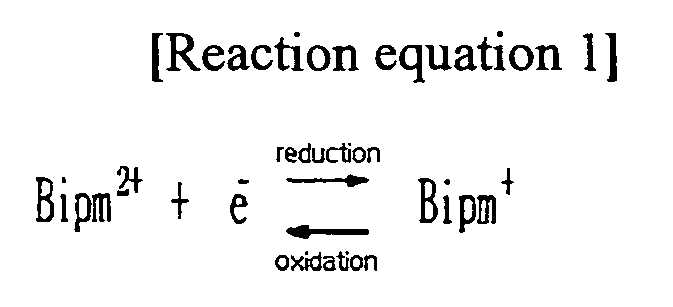
- As can be seen from
chemical equation 1 below, if the viologen is subjected to the first voltage, the viologen reacts to change its color from a transparent state to a deep black. In thechemical equation 1, each of R1 and R2 indicates a phenyl group or an alkyl group having 1 to 10 carbon atoms. Likewise, if oxidation reaction is generated, the viologen changes its color from a deep black to a transparent state.

- To summaries, if the first predetermined voltage is applied between the first
transparent electrode 516 and the secondtransparent electrode 517, a reduction reaction may be generated in the electrochromic layer, the electrochromic layer consequently changes its color from a transparent state to a deep black to serve as a black matrix and the organiclight emitting display 530 according emits light only from a front side (i.e., the top side in FIG. 7). Also, when oxidation reaction is generated in the electrochromic layer, the electrochromic layer changes its color from a deep black to a transparent state and theOLED 530 emits light from both sides. - FIG. 8 is a schematic sectional view illustrating another state in which a predetermined voltage (a second voltage) is applied to an organic
light emitting display 530 according to the third embodiment of the present invention. - Referring to FIG. 8, the second voltage higher than the first voltage in FIG. 5 is applied between a first
transparent electrode 516 and a secondtransparent electrode 517 by a switch (not shown) provided on thecontroller 520. -
Reaction equation 2 is a reduction and oxidation reaction equation of a viologen derivative such as can be used in the electrochromatice layer when the second voltage is applied to the viologen. The viologen supplied with the first voltage enters a Bipm+ state to indicate a deep black, but if the second voltage higher than the first voltage is applied to the viologen, the viologen changes its color to a light black. Likewise, if oxidation reaction is generated, the viologen changes its color from a light black to a deep black.
- As can be seen from
chemical equation 2 below, if the viologen applied with the first voltage is applied with the second voltage higher than the first voltage, the viologen reacts to change its color from a deep black to a light black. In thechemical equation 2, each of R1 and R2 indicates a phenyl group or an alkyl group having 1 to 10 carbon atoms. Likewise, if an oxidation reaction is generated, the viologen changes its color from a light black to a deep black.
- Consequently, if a higher voltage is applied between the first
transparent electrode 516 and the secondtransparent electrode 517, when reduction reaction is generated in the electrochromic layer, the electrochromic layer changes its color from a deep black to a light black to indicate gray tone. Also, when oxidation reaction is generated in the electrochromic layer, the electrochromic layer changes its color from a light black to a deep black so that light can be transmitted only from a front side. - As another example, reaction equation 3 below is anode compound reaction equation of metallocene. In the reaction equation 3, M indicates a metal.


- The examples of the
coloring agent 519 of the electrochromic layer may include many substances such as an aromatic amine, an oxidation reduction complex, phtalocyanine, a heterocyclic compound, fluoran, styryl, anthraquinone, or phtalicdiester, etc. Theelectrolyte 418 may include aqueous or non-aqueous liquid (electrolyte) and semi-solid (high polymer electrolyte), etc. - The organic light emitting display according to an embodiment of the present invention consequently controls the voltage applied to the electrochromic layer, enabling it to selectively display an image on its front side (front side emission) or both sides (double-sided emission).
- An organic light emitting display according to an embodiment of the present invention is further provided with an optical sensor or a voice sensor, enabling it to freely display an image in response on light or voice.
- In above-described embodiments, the TFT and the aperture overlap each other. However, the TFT and the aperture need not overlap each other. Also, in relation to the above-described embodiments, the coplanar TFT has been described. However, the present invention can be applied to a reverse coplanar structure, a staggered structure, and a reverse staggered structure.
- As described above, the present invention relates to a flat panel display and a method of driving the same which can maintain an opaque state when required, while maintaining a transparent state at other times. This is achieved by providing a transparent double-sided emission panel and a controlling unit on the lower portion of the transparent double-sided emission panel, thereby enabling it to selectively display an image on both sides or one side and also to improve image illuminance.
- Although the preferred embodiments of the present invention have been disclosed for illustrative purposes, those skilled in the art will appreciate that various modifications, additions and substitutions are possible, without departing from the scope and spirit of the invention as defined in the accompanying claims.
Claims (22)
- A flat panel display (FPD), comprising:an at least partly transparent and double-sided emission panel including a transparent thin film transistor; anda controlling unit connected to the emission panel, the controlling unit comprising an electrochromic device having a coloring agent, the controlling unit being arranged to control transmission of light therethrough by changing the color of the coloring agent, the color of the coloring agent being changed when a voltage is applied.
- A FPD according to claim 1, wherein the color of the coloring agent is arranged to be changed depending on oxidation and reduction reactions of the coloring agent when the voltage is applied.
- A FPD according to claim 1 or 2, wherein the controlling unit is adapted to control transmission of light to display an image selectively on one side or both sides of the FPD by controlling the voltage to the coloring agent.
- A FPD according to any one of claims 1 to 3, wherein the FPD is an organic light emitting display, and the at least one transparent thin film transistor is for driving the organic light emitting unit.
- A FPD according to any one of claims 1 to 4, wherein the electrochromic device comprises:a first transparent substrate connected to one side of the emission panel;a first transparent electrode mounted on the first transparent substrate;a second transparent electrode separated from the first transparent electrode by a predetermined distance and facing the first transparent electrode;a second transparent substrate on which the second transparent electrode is mounted; whereinthe electrochromic device comprises an electrolytic layer containing the coloring agent located between the first transparent electrode and the second transparent electrode.
- A FPD according to claim 5, wherein the electrochromic device further comprises a controller for controlling a voltage between the first transparent electrode and the second transparent electrode.
- A FPD according to claim 6, wherein the controller further comprises a switch for changing said voltage.
- A FPD according to any one of claims 1 to 7, wherein the coloring agent is black when the voltage is applied to make the FPD an one-sided emission display, and the coloring agent is transparent when the voltage is not applied to make the FPD a double-sided emission display.
- A FPD according to any one of claims 6 to 8, wherein the controller for controlling the voltage is adapted to supply at least two different voltages comprising a first voltage and a second voltage, and wherein the coloring agent is transparent when the voltage is not applied, the coloring agent is a first color when the first voltage is applied, and the coloring agent is a second color different from the first color when the second voltage higher than the first voltage is applied.
- A FPD according to any one of claims 5 to 9, further comprising a sealing member formed around the first transparent substrate and the second transparent substrate arranged to prevent a leak of the electrolytic layer and to bond the first transparent substrate and the second transparent substrate.
- A FPD according to any one of claims 5 to 10, further comprising spacers formed between the first transparent substrate and the second transparent substrate arranged to maintain a predetermined distance between the first transparent substrate and the second transparent substrate.
- A FPD according to any one of claims 5 to 11, wherein the thickness between the first transparent substrate and the second transparent substrate is in the range of 10 to 100µm.
- A FPD according to any one of claims 5 to 12, wherein the coloring agent is selected from the group consisting of a viologen derivative, metallocene(M(C5 G5)2), a derivative of metallocene, aromatic amine, an oxidation reduction complex, phtalocyanine, a heterocyclic compound, fluoran, styryl, anthraquinone, and phtalicdiester.
- A FPD according to any one of claims 5 to 13, wherein the electrolytic layer is selected from the group consisting of aqueous liquid, non-aqueous liquid high polymer electrolyte.
- A FPD according to any preceding claim, wherein the FPD is an organic light emitting display.
- An organic light emitting display (OLED) comprising:a display unit comprising an organic light emitting unit and at least a transparent thin film transistor for driving the organic light emitting unit; anda controlling unit formed below the display unit, the controlling unit comprising:a first transparent substrate connected to the display unit;a first transparent electrode mounted on the first transparent substrate;a second transparent electrode separated from the first transparent electrode by a predetermined distance and facing the first transparent electrode;a second transparent substrate on which the second transparent electrode is mounted; the organic light emitting display further comprising:an electrochromic device comprising an electrolytic layer containing a coloring agent located between the first transparent electrode and the second transparent electrode, the electrochromic device being adapted to control transmission of light by changing color of the coloring agent, the color of the coloring agent being changed depending on oxidation and reduction reactions of the coloring agent when voltage is applied.
- An OLED according to claim 16, wherein the controlling unit further comprises a controller for controlling the voltage between the first transparent electrode or the second transparent electrode.
- An OLED according to claim 16 or 17, wherein the controller further comprises a switch for changing said voltage.
- An OLED according to any one of claims 16 to 18, wherein the transparent thin film transistor comprises a transparent semiconductor layer, a transparent gate electrode, and transparent source and drain electrodes.
- An OLED according to claim 19, wherein the transparent gate electrode and the transparent source and drain electrodes are independently selected from the group consisting of indium tin oxide (ITO), indium zinc oxide (IZO) and indium tin zinc oxide (ITZO).
- An OELD according to claim 19 or 20, wherein the transparent semiconductor layer included in the transparent thin film transistor is formed of semiconductor material which has a wide band gap of at least 3.0eV.
- An OELD according to claim 21, wherein the semiconductor material is formed of at least one selected from the group consisting of oxides such as ZnO, ZnSnO, CdSnO, GaSnO, TlSnO, InGaZnO, CuAlO, SrCuO, and LaCuOS, nitrides such as GaN, InGaN, AlGaN, and InGaAlN, and carbides such as SiC and diamond, etc.
Applications Claiming Priority (2)
| Application Number | Priority Date | Filing Date | Title |
|---|---|---|---|
| KR1020050090740A KR100739297B1 (en) | 2005-09-28 | 2005-09-28 | Flat Panel Display and Driving Method |
| KR1020050090739A KR100646949B1 (en) | 2005-09-28 | 2005-09-28 | Flat Panel Display and Driving Method |
Publications (1)
| Publication Number | Publication Date |
|---|---|
| EP1770673A1 true EP1770673A1 (en) | 2007-04-04 |
Family
ID=37564339
Family Applications (2)
| Application Number | Title | Priority Date | Filing Date |
|---|---|---|---|
| EP06255014A Withdrawn EP1770673A1 (en) | 2005-09-28 | 2006-09-28 | Flat panel display and a method of driving the same |
| EP06255013A Withdrawn EP1770672A1 (en) | 2005-09-28 | 2006-09-28 | Flat panel display and a method of driving the same |
Family Applications After (1)
| Application Number | Title | Priority Date | Filing Date |
|---|---|---|---|
| EP06255013A Withdrawn EP1770672A1 (en) | 2005-09-28 | 2006-09-28 | Flat panel display and a method of driving the same |
Country Status (2)
| Country | Link |
|---|---|
| US (2) | US20070069995A1 (en) |
| EP (2) | EP1770673A1 (en) |
Families Citing this family (49)
| Publication number | Priority date | Publication date | Assignee | Title |
|---|---|---|---|---|
| KR100719706B1 (en) * | 2005-09-13 | 2007-05-17 | 삼성에스디아이 주식회사 | Flat panel display and organic light emitting display |
| EP1770673A1 (en) | 2005-09-28 | 2007-04-04 | Samsung SDI Co., Ltd. | Flat panel display and a method of driving the same |
| TWI442368B (en) | 2006-10-26 | 2014-06-21 | 半導體能源研究所股份有限公司 | Electronic device, display device, and semiconductor device, and driving method thereof |
| KR100841362B1 (en) * | 2006-11-10 | 2008-06-26 | 삼성에스디아이 주식회사 | Organic light emitting display device and manufacturing method thereof |
| US20080172197A1 (en) * | 2007-01-11 | 2008-07-17 | Motorola, Inc. | Single laser multi-color projection display with quantum dot screen |
| JP4727684B2 (en) * | 2007-03-27 | 2011-07-20 | 富士フイルム株式会社 | Thin film field effect transistor and display device using the same |
| US20090001881A1 (en) * | 2007-06-28 | 2009-01-01 | Masaya Nakayama | Organic el display and manufacturing method thereof |
| JP2010538413A (en) * | 2007-08-27 | 2010-12-09 | コーニンクレッカ フィリップス エレクトロニクス エヌ ヴィ | Optical output device |
| KR100911979B1 (en) * | 2008-03-13 | 2009-08-13 | 삼성모바일디스플레이주식회사 | Organic light emitting display device and driving method thereof |
| CN102023433B (en) | 2009-09-18 | 2012-02-29 | 北京京东方光电科技有限公司 | TFT-LCD array substrate and method for manufacturing the same |
| KR101084181B1 (en) * | 2010-01-05 | 2011-11-17 | 삼성모바일디스플레이주식회사 | Organic light emitting display |
| KR101156440B1 (en) * | 2010-03-09 | 2012-06-18 | 삼성모바일디스플레이주식회사 | Organic light emitting display |
| KR20110101980A (en) * | 2010-03-10 | 2011-09-16 | 삼성모바일디스플레이주식회사 | OLED display and manufacturing method thereof |
| JP5947000B2 (en) * | 2010-07-01 | 2016-07-06 | 株式会社半導体エネルギー研究所 | Electric field drive type display device |
| KR101716278B1 (en) * | 2010-09-14 | 2017-03-27 | 에스프린팅솔루션 주식회사 | Image forming apparatus, printing control terminal apparatus and image forming method there of |
| US8723835B2 (en) * | 2010-11-30 | 2014-05-13 | Au Optronics Corporation | Touch-sensing display panel, touch panel, touch-sensing device and touch-sensing circuit |
| KR101798488B1 (en) * | 2010-12-14 | 2017-11-17 | 삼성디스플레이 주식회사 | Organic light emitting display |
| US9006803B2 (en) | 2011-04-22 | 2015-04-14 | Semiconductor Energy Laboratory Co., Ltd. | Semiconductor device and method for manufacturing thereof |
| US8878288B2 (en) | 2011-04-22 | 2014-11-04 | Semiconductor Energy Laboratory Co., Ltd. | Semiconductor device |
| US8932913B2 (en) | 2011-04-22 | 2015-01-13 | Semiconductor Energy Laboratory Co., Ltd. | Manufacturing method of semiconductor device |
| US8809854B2 (en) | 2011-04-22 | 2014-08-19 | Semiconductor Energy Laboratory Co., Ltd. | Semiconductor device |
| US8916868B2 (en) | 2011-04-22 | 2014-12-23 | Semiconductor Energy Laboratory Co., Ltd. | Semiconductor device and method for manufacturing semiconductor device |
| US8847233B2 (en) | 2011-05-12 | 2014-09-30 | Semiconductor Energy Laboratory Co., Ltd. | Semiconductor device having a trenched insulating layer coated with an oxide semiconductor film |
| TWI449006B (en) * | 2011-10-05 | 2014-08-11 | Ind Tech Res Inst | Hybrid display device |
| KR101420479B1 (en) * | 2011-10-31 | 2014-07-17 | 엘지디스플레이 주식회사 | Organic light-emitting display device |
| US9099665B2 (en) * | 2011-12-16 | 2015-08-04 | Samsung Display Co., Ltd. | Organic electro-luminescence display device |
| KR20130088686A (en) * | 2012-01-31 | 2013-08-08 | 삼성전자주식회사 | Display apparatus, display panel and method thereof |
| CN102751312B (en) * | 2012-07-27 | 2015-10-28 | 南京中电熊猫液晶显示科技有限公司 | A kind of OLED display and manufacture method thereof |
| US9354470B2 (en) * | 2013-09-24 | 2016-05-31 | Gentex Corporation | Electro-optic device |
| US10026368B2 (en) * | 2013-09-25 | 2018-07-17 | Sony Corporation | Display device and electronic apparatus |
| KR20150105706A (en) | 2014-03-10 | 2015-09-18 | 삼성전자주식회사 | Display device |
| KR102167932B1 (en) * | 2015-03-10 | 2020-10-21 | 한국전자통신연구원 | Complex display device |
| US9666118B2 (en) * | 2015-10-01 | 2017-05-30 | Chunghwa Picture Tubes, Ltd. | Transparent display apparatus |
| US10418555B2 (en) * | 2015-10-01 | 2019-09-17 | Phillips 66 Company | Formation of films for organic photovoltaics |
| KR102449405B1 (en) * | 2015-12-04 | 2022-09-29 | 엘지디스플레이 주식회사 | Transparent display device, and method for fabricating the same |
| KR102526534B1 (en) | 2015-12-31 | 2023-04-26 | 엘지디스플레이 주식회사 | Transparent display device |
| CN105789256A (en) * | 2016-03-18 | 2016-07-20 | 京东方科技集团股份有限公司 | OLED (organic light-emitting diode) two-sided display substrate, manufacturing method, and display |
| TWI730018B (en) * | 2016-09-06 | 2021-06-11 | 日商半導體能源硏究所股份有限公司 | Display device, input/output device, semiconductor device |
| KR102599536B1 (en) * | 2017-01-26 | 2023-11-08 | 삼성전자 주식회사 | Electronic device having a biometric sensor |
| CN107799017A (en) * | 2017-11-08 | 2018-03-13 | 武汉华星光电半导体显示技术有限公司 | Display with double faces and preparation method thereof |
| KR102592652B1 (en) * | 2018-06-11 | 2023-10-24 | 엘지전자 주식회사 | Mobile terminal |
| CN108681132B (en) * | 2018-06-29 | 2021-03-02 | Tcl华星光电技术有限公司 | display device |
| CN110767693B (en) * | 2018-12-14 | 2022-07-19 | 昆山国显光电有限公司 | Array substrate, display screen and display terminal |
| CN109887981B (en) * | 2019-03-20 | 2021-02-23 | 业成科技(成都)有限公司 | Organic light emitting diode display panel and manufacturing method thereof |
| CN110335806A (en) * | 2019-06-17 | 2019-10-15 | 武汉华星光电技术有限公司 | The preparation method and thin film transistor (TFT) of conducting channel material |
| EP4258248A4 (en) * | 2020-12-07 | 2024-11-20 | Agc Inc. | TRANSPARENT DISPLAY DEVICE, LAMINATED GLASS AND METHOD FOR PRODUCING A TRANSPARENT DISPLAY DEVICE |
| CN114220837B (en) * | 2021-12-13 | 2023-08-01 | 深圳市华星光电半导体显示技术有限公司 | Double-sided display panel, preparation method of double-sided display panel and electronic equipment |
| CN115802823A (en) * | 2022-12-16 | 2023-03-14 | 固安翌光科技有限公司 | A double-sided display panel and a double-sided display device |
| TWI866595B (en) | 2023-11-09 | 2024-12-11 | 友達光電股份有限公司 | Transparent display apparatus |
Citations (8)
| Publication number | Priority date | Publication date | Assignee | Title |
|---|---|---|---|---|
| JP2001332392A (en) * | 2000-05-19 | 2001-11-30 | Sony Corp | Double-sided organic electroluminescent device, double-sided organic electroluminescent display device and electronic equipment |
| WO2002071131A2 (en) * | 2000-10-23 | 2002-09-12 | Motorola Inc., A Corporation Of The State Of Delaware | Double-sided viewable display with switchable transflector |
| US20040155846A1 (en) * | 2003-02-07 | 2004-08-12 | Randy Hoffman | Transparent active-matrix display |
| US20040245531A1 (en) * | 2003-01-24 | 2004-12-09 | Teruyuki Fuii | Lighting emitting device, manufacturing method of the same, electronic apparatus having the same |
| EP1510994A1 (en) * | 2003-08-21 | 2005-03-02 | Pioneer Corporation | Display system and electronic appliance including the display |
| JP2005208125A (en) * | 2004-01-20 | 2005-08-04 | Toshiba Lsi System Support Kk | Image display device and electronic device equipped with the same |
| WO2005088594A1 (en) * | 2004-03-12 | 2005-09-22 | Fujitsu Limited | Display and method for driving same |
| EP1763082A2 (en) * | 2005-09-13 | 2007-03-14 | Samsung SDI Co., Ltd. | Flat panel display and organic light emitting display |
Family Cites Families (14)
| Publication number | Priority date | Publication date | Assignee | Title |
|---|---|---|---|---|
| JPH0854832A (en) | 1994-06-10 | 1996-02-27 | Nippondenso Co Ltd | Transparent thin film EL display |
| JP3667242B2 (en) * | 2000-04-13 | 2005-07-06 | キヤノン株式会社 | Electrophoretic display method and electrophoretic display device |
| JP3719172B2 (en) * | 2000-08-31 | 2005-11-24 | セイコーエプソン株式会社 | Display device and electronic device |
| US7038670B2 (en) * | 2002-08-16 | 2006-05-02 | Sipix Imaging, Inc. | Electrophoretic display with dual mode switching |
| JP4090716B2 (en) * | 2001-09-10 | 2008-05-28 | 雅司 川崎 | Thin film transistor and matrix display device |
| JP2004014982A (en) | 2002-06-11 | 2004-01-15 | Konica Minolta Holdings Inc | Semiconductor circuit and image display device |
| US6972516B2 (en) * | 2002-06-14 | 2005-12-06 | University Of Cincinnati | Photopump-enhanced electroluminescent devices |
| KR100527198B1 (en) * | 2003-11-12 | 2005-11-08 | 삼성에스디아이 주식회사 | flat panel display for displaying screens at both sides |
| DE102004003760B4 (en) | 2004-01-23 | 2014-05-22 | Forschungszentrum Jülich GmbH | A process for producing a conductive and transparent zinc oxide layer and use thereof in a thin film solar cell |
| KR100700004B1 (en) * | 2004-11-10 | 2007-03-26 | 삼성에스디아이 주식회사 | Double-sided light emitting organic electroluminescent device and manufacturing method thereof |
| KR100719540B1 (en) * | 2004-11-18 | 2007-05-17 | 삼성에스디아이 주식회사 | Supporting device for flat panel display panel and flat panel display device having same |
| KR100731738B1 (en) * | 2005-03-30 | 2007-06-22 | 삼성에스디아이 주식회사 | Thin film transistor, flat panel display and manufacturing method |
| EP1770673A1 (en) | 2005-09-28 | 2007-04-04 | Samsung SDI Co., Ltd. | Flat panel display and a method of driving the same |
| KR100732849B1 (en) * | 2005-12-21 | 2007-06-27 | 삼성에스디아이 주식회사 | Organic light emitting display |
-
2006
- 2006-09-28 EP EP06255014A patent/EP1770673A1/en not_active Withdrawn
- 2006-09-28 US US11/528,419 patent/US20070069995A1/en not_active Abandoned
- 2006-09-28 EP EP06255013A patent/EP1770672A1/en not_active Withdrawn
- 2006-09-28 US US11/528,414 patent/US7463399B2/en active Active
Patent Citations (8)
| Publication number | Priority date | Publication date | Assignee | Title |
|---|---|---|---|---|
| JP2001332392A (en) * | 2000-05-19 | 2001-11-30 | Sony Corp | Double-sided organic electroluminescent device, double-sided organic electroluminescent display device and electronic equipment |
| WO2002071131A2 (en) * | 2000-10-23 | 2002-09-12 | Motorola Inc., A Corporation Of The State Of Delaware | Double-sided viewable display with switchable transflector |
| US20040245531A1 (en) * | 2003-01-24 | 2004-12-09 | Teruyuki Fuii | Lighting emitting device, manufacturing method of the same, electronic apparatus having the same |
| US20040155846A1 (en) * | 2003-02-07 | 2004-08-12 | Randy Hoffman | Transparent active-matrix display |
| EP1510994A1 (en) * | 2003-08-21 | 2005-03-02 | Pioneer Corporation | Display system and electronic appliance including the display |
| JP2005208125A (en) * | 2004-01-20 | 2005-08-04 | Toshiba Lsi System Support Kk | Image display device and electronic device equipped with the same |
| WO2005088594A1 (en) * | 2004-03-12 | 2005-09-22 | Fujitsu Limited | Display and method for driving same |
| EP1763082A2 (en) * | 2005-09-13 | 2007-03-14 | Samsung SDI Co., Ltd. | Flat panel display and organic light emitting display |
Also Published As
| Publication number | Publication date |
|---|---|
| US20070075943A1 (en) | 2007-04-05 |
| US20070069995A1 (en) | 2007-03-29 |
| US7463399B2 (en) | 2008-12-09 |
| EP1770672A1 (en) | 2007-04-04 |
Similar Documents
| Publication | Publication Date | Title |
|---|---|---|
| US7463399B2 (en) | Flat panel display and a method of driving the same | |
| US7719185B2 (en) | Flat panel display and driving method using the same | |
| EP1763082A2 (en) | Flat panel display and organic light emitting display | |
| US8227797B2 (en) | Transparent display apparatus | |
| US20130271445A1 (en) | Dual mode display device | |
| US9236577B2 (en) | Dual-mode display device and method of manufacturing same | |
| US12274118B2 (en) | Substrate assembly and display device | |
| US20170186829A1 (en) | Flexible device, display device, and manufacturing methods thereof | |
| KR20140127695A (en) | Transparent display device | |
| KR20120127085A (en) | Display device | |
| US8836907B2 (en) | Liquid crystal display device | |
| KR20210086338A (en) | Light Emitting Display Device | |
| KR20090110174A (en) | Display device and its operation method | |
| US20130057944A1 (en) | Flat panel display apparatus | |
| US20090153939A1 (en) | Color display device | |
| KR101878926B1 (en) | apparatus for displaying dual mode and manufacturing method of the same | |
| KR100646949B1 (en) | Flat Panel Display and Driving Method | |
| KR100739297B1 (en) | Flat Panel Display and Driving Method | |
| US10216999B2 (en) | Display system, electronic device, and display method | |
| KR101897249B1 (en) | apparatus for displaying dual mode and manufacturing method of the same | |
| KR102349592B1 (en) | Thin film transistor, Array substrate and Reflective display device including the same | |
| KR20130005489A (en) | Organic light emitting diode display and method for controlling thereof | |
| US12517400B2 (en) | Display device | |
| KR20080001946A (en) | Organic electroluminescent display and its driving method |
Legal Events
| Date | Code | Title | Description |
|---|---|---|---|
| PUAI | Public reference made under article 153(3) epc to a published international application that has entered the european phase |
Free format text: ORIGINAL CODE: 0009012 |
|
| 17P | Request for examination filed |
Effective date: 20061005 |
|
| AK | Designated contracting states |
Kind code of ref document: A1 Designated state(s): AT BE BG CH CY CZ DE DK EE ES FI FR GB GR HU IE IS IT LI LT LU LV MC NL PL PT RO SE SI SK TR |
|
| AX | Request for extension of the european patent |
Extension state: AL BA HR MK YU |
|
| AKX | Designation fees paid |
Designated state(s): DE FR GB |
|
| RAP1 | Party data changed (applicant data changed or rights of an application transferred) |
Owner name: SAMSUNG MOBILE DISPLAY CO., LTD. |
|
| 17Q | First examination report despatched |
Effective date: 20090424 |
|
| RAP1 | Party data changed (applicant data changed or rights of an application transferred) |
Owner name: SAMSUNG DISPLAY CO., LTD. |
|
| RAP1 | Party data changed (applicant data changed or rights of an application transferred) |
Owner name: SAMSUNG DISPLAY CO., LTD. |
|
| STAA | Information on the status of an ep patent application or granted ep patent |
Free format text: STATUS: THE APPLICATION IS DEEMED TO BE WITHDRAWN |
|
| 18D | Application deemed to be withdrawn |
Effective date: 20160826 |