EP1768186A2 - Method of making a self-aligned photodiode for CMOS image sensor - Google Patents
Method of making a self-aligned photodiode for CMOS image sensor Download PDFInfo
- Publication number
- EP1768186A2 EP1768186A2 EP06254811A EP06254811A EP1768186A2 EP 1768186 A2 EP1768186 A2 EP 1768186A2 EP 06254811 A EP06254811 A EP 06254811A EP 06254811 A EP06254811 A EP 06254811A EP 1768186 A2 EP1768186 A2 EP 1768186A2
- Authority
- EP
- European Patent Office
- Prior art keywords
- gate stack
- layer
- photodiode
- forming
- polysilicon
- Prior art date
- Legal status (The legal status is an assumption and is not a legal conclusion. Google has not performed a legal analysis and makes no representation as to the accuracy of the status listed.)
- Ceased
Links
- 238000004519 manufacturing process Methods 0.000 title description 4
- 238000000034 method Methods 0.000 claims abstract description 45
- 239000012212 insulator Substances 0.000 claims abstract description 37
- 238000012546 transfer Methods 0.000 claims abstract description 32
- XUIMIQQOPSSXEZ-UHFFFAOYSA-N Silicon Chemical compound [Si] XUIMIQQOPSSXEZ-UHFFFAOYSA-N 0.000 claims abstract description 20
- 229910021420 polycrystalline silicon Inorganic materials 0.000 claims abstract description 20
- 229920005591 polysilicon Polymers 0.000 claims abstract description 20
- 229910052710 silicon Inorganic materials 0.000 claims abstract description 20
- 239000010703 silicon Substances 0.000 claims abstract description 20
- 229910052751 metal Inorganic materials 0.000 claims abstract description 18
- 239000002184 metal Substances 0.000 claims abstract description 18
- 229910021332 silicide Inorganic materials 0.000 claims abstract description 15
- FVBUAEGBCNSCDD-UHFFFAOYSA-N silicide(4-) Chemical compound [Si-4] FVBUAEGBCNSCDD-UHFFFAOYSA-N 0.000 claims abstract description 15
- 230000015572 biosynthetic process Effects 0.000 claims abstract description 12
- VYPSYNLAJGMNEJ-UHFFFAOYSA-N Silicium dioxide Chemical compound O=[Si]=O VYPSYNLAJGMNEJ-UHFFFAOYSA-N 0.000 claims abstract description 11
- 235000012239 silicon dioxide Nutrition 0.000 claims abstract description 4
- 239000000377 silicon dioxide Substances 0.000 claims abstract description 4
- 239000000758 substrate Substances 0.000 claims description 17
- 239000004065 semiconductor Substances 0.000 claims description 10
- 125000006850 spacer group Chemical group 0.000 claims description 10
- 230000001681 protective effect Effects 0.000 claims description 9
- 229910017052 cobalt Inorganic materials 0.000 claims description 5
- 239000010941 cobalt Substances 0.000 claims description 5
- GUTLYIVDDKVIGB-UHFFFAOYSA-N cobalt atom Chemical compound [Co] GUTLYIVDDKVIGB-UHFFFAOYSA-N 0.000 claims description 5
- 238000013461 design Methods 0.000 claims description 4
- 238000005530 etching Methods 0.000 claims description 4
- 239000002019 doping agent Substances 0.000 claims description 3
- 229910052814 silicon oxide Inorganic materials 0.000 claims description 3
- 229910021341 titanium silicide Inorganic materials 0.000 claims description 3
- 229910052581 Si3N4 Inorganic materials 0.000 claims description 2
- 229910044991 metal oxide Inorganic materials 0.000 claims description 2
- 150000004706 metal oxides Chemical group 0.000 claims description 2
- HQVNEWCFYHHQES-UHFFFAOYSA-N silicon nitride Chemical compound N12[Si]34N5[Si]62N3[Si]51N64 HQVNEWCFYHHQES-UHFFFAOYSA-N 0.000 claims description 2
- 230000000873 masking effect Effects 0.000 claims 1
- 239000010410 layer Substances 0.000 description 47
- 239000007943 implant Substances 0.000 description 40
- 229920002120 photoresistant polymer Polymers 0.000 description 9
- 230000010354 integration Effects 0.000 description 5
- 238000002955 isolation Methods 0.000 description 5
- 238000000059 patterning Methods 0.000 description 5
- 239000006117 anti-reflective coating Substances 0.000 description 4
- 230000003321 amplification Effects 0.000 description 3
- 238000000151 deposition Methods 0.000 description 3
- 230000008021 deposition Effects 0.000 description 3
- 239000000463 material Substances 0.000 description 3
- 238000003199 nucleic acid amplification method Methods 0.000 description 3
- NBIIXXVUZAFLBC-UHFFFAOYSA-N Phosphoric acid Chemical compound OP(O)(O)=O NBIIXXVUZAFLBC-UHFFFAOYSA-N 0.000 description 2
- RTAQQCXQSZGOHL-UHFFFAOYSA-N Titanium Chemical compound [Ti] RTAQQCXQSZGOHL-UHFFFAOYSA-N 0.000 description 2
- 239000011248 coating agent Substances 0.000 description 2
- 238000000576 coating method Methods 0.000 description 2
- 238000010438 heat treatment Methods 0.000 description 2
- BHEPBYXIRTUNPN-UHFFFAOYSA-N hydridophosphorus(.) (triplet) Chemical compound [PH] BHEPBYXIRTUNPN-UHFFFAOYSA-N 0.000 description 2
- 150000002500 ions Chemical class 0.000 description 2
- 150000004767 nitrides Chemical class 0.000 description 2
- 239000010936 titanium Substances 0.000 description 2
- 229910052719 titanium Inorganic materials 0.000 description 2
- ZOXJGFHDIHLPTG-UHFFFAOYSA-N Boron Chemical compound [B] ZOXJGFHDIHLPTG-UHFFFAOYSA-N 0.000 description 1
- 238000009825 accumulation Methods 0.000 description 1
- 229910000147 aluminium phosphate Inorganic materials 0.000 description 1
- 238000003491 array Methods 0.000 description 1
- 229910052785 arsenic Inorganic materials 0.000 description 1
- RQNWIZPPADIBDY-UHFFFAOYSA-N arsenic atom Chemical compound [As] RQNWIZPPADIBDY-UHFFFAOYSA-N 0.000 description 1
- 229910052796 boron Inorganic materials 0.000 description 1
- 230000001413 cellular effect Effects 0.000 description 1
- 238000005229 chemical vapour deposition Methods 0.000 description 1
- 238000005516 engineering process Methods 0.000 description 1
- 238000003384 imaging method Methods 0.000 description 1
- 238000002513 implantation Methods 0.000 description 1
- 229910052738 indium Inorganic materials 0.000 description 1
- APFVFJFRJDLVQX-UHFFFAOYSA-N indium atom Chemical compound [In] APFVFJFRJDLVQX-UHFFFAOYSA-N 0.000 description 1
- 238000012986 modification Methods 0.000 description 1
- 230000004048 modification Effects 0.000 description 1
- 238000002161 passivation Methods 0.000 description 1
- 238000000206 photolithography Methods 0.000 description 1
- 238000005498 polishing Methods 0.000 description 1
- 238000012545 processing Methods 0.000 description 1
- 238000003672 processing method Methods 0.000 description 1
- 239000011253 protective coating Substances 0.000 description 1
- 239000011241 protective layer Substances 0.000 description 1
- 239000002023 wood Substances 0.000 description 1
Images




Classifications
-
- H—ELECTRICITY
- H10—SEMICONDUCTOR DEVICES; ELECTRIC SOLID-STATE DEVICES NOT OTHERWISE PROVIDED FOR
- H10F—INORGANIC SEMICONDUCTOR DEVICES SENSITIVE TO INFRARED RADIATION, LIGHT, ELECTROMAGNETIC RADIATION OF SHORTER WAVELENGTH OR CORPUSCULAR RADIATION
- H10F39/00—Integrated devices, or assemblies of multiple devices, comprising at least one element covered by group H10F30/00, e.g. radiation detectors comprising photodiode arrays
- H10F39/011—Manufacture or treatment of image sensors covered by group H10F39/12
- H10F39/014—Manufacture or treatment of image sensors covered by group H10F39/12 of CMOS image sensors
-
- H—ELECTRICITY
- H10—SEMICONDUCTOR DEVICES; ELECTRIC SOLID-STATE DEVICES NOT OTHERWISE PROVIDED FOR
- H10F—INORGANIC SEMICONDUCTOR DEVICES SENSITIVE TO INFRARED RADIATION, LIGHT, ELECTROMAGNETIC RADIATION OF SHORTER WAVELENGTH OR CORPUSCULAR RADIATION
- H10F39/00—Integrated devices, or assemblies of multiple devices, comprising at least one element covered by group H10F30/00, e.g. radiation detectors comprising photodiode arrays
- H10F39/10—Integrated devices
- H10F39/12—Image sensors
- H10F39/18—Complementary metal-oxide-semiconductor [CMOS] image sensors; Photodiode array image sensors
-
- H—ELECTRICITY
- H10—SEMICONDUCTOR DEVICES; ELECTRIC SOLID-STATE DEVICES NOT OTHERWISE PROVIDED FOR
- H10F—INORGANIC SEMICONDUCTOR DEVICES SENSITIVE TO INFRARED RADIATION, LIGHT, ELECTROMAGNETIC RADIATION OF SHORTER WAVELENGTH OR CORPUSCULAR RADIATION
- H10F39/00—Integrated devices, or assemblies of multiple devices, comprising at least one element covered by group H10F30/00, e.g. radiation detectors comprising photodiode arrays
- H10F39/80—Constructional details of image sensors
- H10F39/803—Pixels having integrated switching, control, storage or amplification elements
Definitions
- the present invention relates to image sensors, and more particularly, to an image sensor that uses pixels having photodiodes self-aligned to the transfer gate.
- Image sensors have become ubiquitous. They are widely used in digital still cameras, cellular phones, security cameras, medical, automobile, and other applications.
- the technology used to manufacture image sensors, and in particular CMOS image sensors has continued to advance at great pace. For example, the demands of higher resolution and lower power consumption and cost have encouraged the further miniaturization and integration of the image sensor. Possibly as a result of the greater miniaturization and integration of the image sensor, various issues for both CMOS image sensors have arisen. For example, it is often difficult to maintain uniformity of performance across the millions of pixels in an image sensor pixel array.
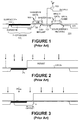
- FIG. 1 shows a cross-sectional view of a prior art active pixel that uses four transistors. This is known in the art as a 4T active pixel.
- a photodiode 101 outputs a signal that is used to modulate an amplification transistor 103.
- the amplification transistor 103 is also referred to as a source follower transistor.
- the photodiode 101 can be either a pinned photodiode or a partially pinned photodiode.
- the photodiode 101 comprises a N- layer 115 that is a buried implant. Additionally, in one embodiment, a shallow P+ pinning layer 116 is formed at the surface of the semiconductor substrate 102.
- various structures are formed atop of and into the silicon substrate 102.
- the photodiode 101 and the floating node 107 are formed into the silicon substrate 102. These structures are said to be formed below the surface of the silicon substrate by the use of dopants.
- field oxides or shallow trench isolation structures are also formed at and below the top surface (or simply surface) of the silicon substrate.
- Other structures, such as the gate oxide 108, the transfer gate 106, the transfer transistor 105, and the reset transistor 113 are formed atop of the silicon substrate 102 and are said to be at or above the top surface of the silicon substrate.
- a transfer transistor 105 is used to transfer the signal output by the photodiode 101 to floating node 107 (N+ doped), which is adjacent to the gate of the transfer transistor 105 and opposite the photodiode 101.
- the transfer transistor 105 is controlled by a transfer gate 106.
- the transfer transistor 105 also has a gate oxide 108 underneath the transfer gate 106.
- the photodiode 101 stores charge that is held in the N- layer 115.
- the transfer transistor 105 is turned on to transfer the charge held in the N- layer 115 of the photodiode 101 to the floating node 107.
- the transfer transistor 105 is turned off again for the start of a subsequent integration period. The signal on the floating node 107 is then used to modulate the amplification transistor 103.
- the photodiode 101 and its implants 115 and 116 are typically not self-aligned to the adjacent transfer gate.
- the surface P+ implant 116 and the buried N- implant 115 oftentimes may or may not be aligned with the transfer gate 106.
- both of these implants are performed prior to the formation of the transfer gate 106.
- a photoresist is patterned over the gate oxide layer.
- the photoresist has an opening that allows for the formation of the surface P+ implant 116.
- the P-type implant typically boron, is then implanted in the opening forming the surface P+ implant layer 116.
- the resist is then stripped.
- new photoresist layer is patterned.
- An N-type implant such as phosphorous, is implanted in the opening forming the buried N- implant layer 115. Note that the lateral offset between the P+ layer 116 and the N-layer 115 varies due to alignment registration errors at both of these patterning steps.
- a gate oxide and a transistor gate stack are formed on the wafer.
- a spacer layer is deposited and etched back using an anisotropic etch and the source/drain regions are implanted as shown in Figure 1.
- the overlap of the N- implant under the adjacent transfer gate and the underlap of the P+ implant 116 to the transfer gate are controlled by alignment registration of the P+ implant reticle, the N- implant reticle, and the transistor gate reticle. This introduces a variability in both the performance of the transfer gate and for charge transfer from the photodiode to the floating node 107.
- the N channel and P channel lightly doped drain (LDD) implants are performed.
- the LDD implants are masked implants with resist covering the photodiode region so that the photodiode is not implanted.
- Sidewall spacers are formed such that the N+ and P+ source/drains can be implanted as seen in Figure 1.
- a protective insulator is deposited typically with a thickness of 100-1,000 ⁇ of oxide.
- the protective insulator is removed from the gate stack using either a resist etch back process or a chemical-mechanical polishing (CMP) process.
- CMP chemical-mechanical polishing
- a photoresist layer is formed which protects the photodiode.
- a metal such as cobalt or titanium is then deposited onto the wafer to a thickness of between 50-300 ⁇ .
- a heat treatment is performed to allow the silicon in contact with the metal to react to form a metal silicide.
- Remaining process steps to complete the imager include dielectric deposition, contact etching, metal and via formation, passivation, bond pad etching, color filter arrays formation, and microlens formation.
- the present invention provides a method of forming a portion of an active pixel according to Claim 1.
- Figure 1 is a cross-sectional view of a prior art four transistor (4T) pixel which shows in detail a photodiode formed in a substrate.
- Figures 2-7 are cross-sectional views of a prior art process for forming a photodiode and pixel of Figure 1.
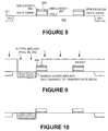
- Figures 8-16 are cross-sectional views of a process for forming a self-aligned photodiode in accordance with one embodiment of the present invention.
- references throughout the specification to "one embodiment” or “an embodiment” means that a particular feature, structure, or characteristic described in connection with the embodiment and included in at least one embodiment of the present invention.
- the appearances of the phrase “in one embodiment” or “in an embodiment” in various places throughout the specification are not necessarily all referring to the same embodiment.
- the particular features, structures, or characteristics may be combined in any suitable manner in one or more embodiments.
- the photodiode design and process of the present invention can be used with any type of pixel design, including but not limited to 3T, 4T, 5T, 6T, 7T, and other designs.
- the present invention is a pixel for an image sensor that has the photodiode self-aligned with the transfer gate. Further, the self-aligned process is consistent with the other required elements of the manufacturing process flow. For example, many image sensors use a manufacturing process that use a metal salicide process to improve the speed of periphery transistors and to provide a low resistance routing line. However, the photodiode sensor region should be protected from this salicide process. If the photodiode were to be silicided, the performance of the pixel would be degraded since a cobalt silicide or a titanium silicide is opaque to light and wood block light to the underlying photodiode. The silicide would also increase dark current at the photodiode. For these reasons, as described above, a protective coating such as oxide is placed over the photodiode and over a substantial portion of the imaging array to protect a sensitive region from the silicide process.
- the salicide formation process should be placed in the process flow after the spacer etch and after all the implant steps are completed. This is because the implant steps require high temperatures to activate the dopants and without a spacer in place there may be shorts between the source/drain regions and the transistor gate during the salicide formation.
- my co-pending application entitled "Salicide Process for Image Sensors" filed February 14, 2005 and accorded U.S. Patent Application No. 11/058,117 provides a good exposition on the salicide process, which is herein incorporated by reference.
- the salicide process requires that the photodiode region be protected by a protective layer, such as an oxide. This oxide deposited over the photodiode and the transfer gate prevents any subsequent implant from being aligned to the transfer gate edge.
- One method of forming a self-aligned pinned photodiode is to use a very thick polysilicon deposition as part of the transistor gate formation. However, this increases the stack height of the imager and degrades performance.
- the polysilicon also has grains that are aligned in different crystallographic directions. The high energy buried N- implant can channel through appropriately oriented grains and result in unwanted variations in transistor gate performance.
- a semiconductor substrate 102 is shown.
- the semiconductor substrate 102 is a silicon substrate.
- a standard isolation 203 such as a shallow trench isolation (STI) defines an active area within the semiconductor substrate 102.
- the STI is lined with a P-type field implant.
- the isolation 203 is used to electrically isolate an active area that will contain a pixel.
- a transistor gate stack is deposited by the deposition or growth of a relatively thin gate oxide layer using conventional semiconductor processing methods, such as thermal growth or chemical vapor deposition.
- a conductive layer such as a polysilicon layer, is deposited over the gate oxide layer.
- the gate oxide layer is typically 15-100 ⁇ thick and the polysilicon layer is typically between 500 and 2500 ⁇ thick, and more preferably between 1500-2000 ⁇ .
- the polysilicon layer (when patterned, etched, and possibly doped) will serve as the gate of the various transistors such as the transfer transistor 105 or the reset transistor 113.
- first insulator layer 801 and a second insulator layer 802 are deposited over the polysilicon layer.
- the first and second insulator layers 801 and 802 are also referred to as sacrificial, cap, or disposable insulator layers.
- the disposable insulator may be a metal oxide, silicon oxide, silicon oxynitride, silicon nitride, or combination thereof. They may also serve as an antireflection coating that improves patterning resolution at the transistor gate photolithography step.
- the first and second insulator layers 801 and 802 is later removed at an appropriately defined stage in the process to allow the subsequent reaction of a metal deposited onto the polysilicon to form the metal silicide.
- the first insulator layer 801 is a silicon oxynitride of thickness between 400-1200 ⁇ , and in one embodiment between 600-1000 ⁇ .
- the second insulator layer 802 is a deposited silicon oxide layer having a thickness of between 50-400 ⁇ and in one embodiment between 100-200 ⁇ . The use of these materials provides an excellent sacrificial layer that provides good patterning capability for the transistor gate stack 206.
- the disposable insulator layers may be a single nitride or a single silicon oxynitride layer.
- an organic bottom antireflective coating (ARC) layer can be deposited just prior to the photoresist coating to help better define the transistor gates.
- the ARC layer is etched and then the transistor gate stack is etched in the manner described above. The remaining ARC and photoresist is stripped after the transistor gate has been formed.
- the cap silicon oxynitride or cap nitride layers can later be removed after the N- implant for the photodiode. The removal may be done using a wet hot phosphoric acid etch. After removal of these layers, the stack is patterned and etched to leave the gate stack structures shown in Figure 8. These two structures will eventually form the transfer gate 206 and the gate of the reset transistor 113.
- a photoresist layer is deposited and patterned to provide an opening for the photodiode formation.
- the total thickness of the polysilicon, the first insulator layer 801, and the second insulator layer 802 should be thick enough to block the N- buried implant.
- a polysilicon thickness of 1800 ⁇ , a silicon oxynitride thickness of 850 ⁇ , and a silicon dioxide thickness of 150 ⁇ an arsenic implant energy of 180kev or a phosphorous implant energy of 90kev can be effectively blocked.
- the dosage for the N- implant is typically between 1e12 to 7e12 ions/cm 2 .
- the N- implant is buried beneath the surface and is self-aligned to the adjacent transfer gate edge.
- this description discusses the implantation of a photodiode N- implant next to a transfer gate edge, the teachings of the present invention may be used with any self-aligned implants adjacent to, for example, a reset gate, a high dynamic range gate, lateral overflow drain gate, or other adjacent gate structure.
- the second insulator layer 802 can be first removed using a dry or wet oxide etch.
- a wet HF dip which has excellent selectivity to the first insulator layer may be used.
- the first insulator layer is then removed using a dry or wet silicon oxynitride etch.
- a wet phosphoric etch to minimize any reduction to the remaining gate oxide or the silicon surface.
- the surface of the polysilicon layer does not have any remaining insulator.
- the P+ implant dose in one embodiment is 7e12-1e 14, and preferably 1e13-5e13 ions/cm 2 .
- the implant species may be B11, BF2, or indium. If the implant is B11, the implant energy is 15kev or less. If the implant species is BF2, the implant energy is on the order of 10-40kev.
- the removal of the first and second insulator layers 801 and 802 may be done after the P+ implant instead of after the buried N- implant.
- processing can now be used to form the salicide on the new self-aligned photodiode.
- the N channel and P channel LDD implants are performed first.
- a spacer insulator is deposited and an anisotropic spacer etch forms sidewall spacers on both the transfer gate and the reset gate as seen in Figure 12.
- the spacers are then used to act as a mask for the N+ and P+ source/drains regions outside of the photodiode.
- a protective insulator 1301 is formed over the top of the structure of Figure 12.
- the protective insulator is selectively removed from the gate stack using either a resist etch back process or a CMP process to provide the resulting structure of Figure 14.
- a resist mask is used in Figure 15 to remove portions of the protective insulator and oxide over the floating node and other regions.
- a metal such as cobalt or titanium is then deposited onto the wafer and a heat treatment is applied to allow the silicon in contact with the metal to react to form the metal silicide.
- the wafer is then dipped in a wet bath that removes the unreacted metal over the oxide regions and not the formed silicide.
- the result is seen in Figure 16.
Landscapes
- Solid State Image Pick-Up Elements (AREA)
Abstract
Description
- The present invention relates to image sensors, and more particularly, to an image sensor that uses pixels having photodiodes self-aligned to the transfer gate.
- Image sensors have become ubiquitous. They are widely used in digital still cameras, cellular phones, security cameras, medical, automobile, and other applications. The technology used to manufacture image sensors, and in particular CMOS image sensors, has continued to advance at great pace. For example, the demands of higher resolution and lower power consumption and cost have encouraged the further miniaturization and integration of the image sensor. Possibly as a result of the greater miniaturization and integration of the image sensor, various issues for both CMOS image sensors have arisen. For example, it is often difficult to maintain uniformity of performance across the millions of pixels in an image sensor pixel array.
- Currently, the most popular type of CMOS pixel structure is the four transistor active pixel. Figure I shows a cross-sectional view of a prior art active pixel that uses four transistors. This is known in the art as a 4T active pixel. A
photodiode 101, outputs a signal that is used to modulate anamplification transistor 103. Theamplification transistor 103 is also referred to as a source follower transistor. In this embodiment, thephotodiode 101 can be either a pinned photodiode or a partially pinned photodiode. Thephotodiode 101 comprises a N- layer 115 that is a buried implant. Additionally, in one embodiment, a shallowP+ pinning layer 116 is formed at the surface of thesemiconductor substrate 102. - Further, various structures are formed atop of and into the
silicon substrate 102. For example, thephotodiode 101 and thefloating node 107 are formed into thesilicon substrate 102. These structures are said to be formed below the surface of the silicon substrate by the use of dopants. Similarly, field oxides or shallow trench isolation structures are also formed at and below the top surface (or simply surface) of the silicon substrate. Other structures, such as thegate oxide 108, thetransfer gate 106, thetransfer transistor 105, and the reset transistor 113 are formed atop of thesilicon substrate 102 and are said to be at or above the top surface of the silicon substrate. - A
transfer transistor 105 is used to transfer the signal output by thephotodiode 101 to floating node 107 (N+ doped), which is adjacent to the gate of thetransfer transistor 105 and opposite thephotodiode 101. Thetransfer transistor 105 is controlled by atransfer gate 106. Thetransfer transistor 105 also has agate oxide 108 underneath thetransfer gate 106. - In operation, during an integration period (also referred to as an exposure or accumulation period), the
photodiode 101 stores charge that is held in the N- layer 115. After the integration period, thetransfer transistor 105 is turned on to transfer the charge held in the N- layer 115 of thephotodiode 101 to thefloating node 107. After the signal has been transferred to thefloating node 107, thetransfer transistor 105 is turned off again for the start of a subsequent integration period. The signal on thefloating node 107 is then used to modulate theamplification transistor 103. - In the prior art, the
photodiode 101 and itsimplants 115 and 116 are typically not self-aligned to the adjacent transfer gate. Thus, thesurface P+ implant 116 and the buried N- implant 115 oftentimes may or may not be aligned with thetransfer gate 106. In the prior art, both of these implants are performed prior to the formation of thetransfer gate 106. For example, turning to Figure 2, after the active areas and shallow trench isolations (STI) are formed, a photoresist is patterned over the gate oxide layer. The photoresist has an opening that allows for the formation of thesurface P+ implant 116. The P-type implant, typically boron, is then implanted in the opening forming the surfaceP+ implant layer 116. The resist is then stripped. - Next, in Figure 3, new photoresist layer is patterned. An N-type implant, such as phosphorous, is implanted in the opening forming the buried N- implant layer 115. Note that the lateral offset between the
P+ layer 116 and the N-layer 115 varies due to alignment registration errors at both of these patterning steps. Next, a gate oxide and a transistor gate stack are formed on the wafer. A spacer layer is deposited and etched back using an anisotropic etch and the source/drain regions are implanted as shown in Figure 1. - The overlap of the N- implant under the adjacent transfer gate and the underlap of the
P+ implant 116 to the transfer gate are controlled by alignment registration of the P+ implant reticle, the N- implant reticle, and the transistor gate reticle. This introduces a variability in both the performance of the transfer gate and for charge transfer from the photodiode to thefloating node 107. - Further, using conventional steps, the N channel and P channel lightly doped drain (LDD) implants are performed. The LDD implants are masked implants with resist covering the photodiode region so that the photodiode is not implanted. Sidewall spacers are formed such that the N+ and P+ source/drains can be implanted as seen in Figure 1.
- Next, turning to Figure 4, in the prior art, in a salicide process, a protective insulator is deposited typically with a thickness of 100-1,000Å of oxide. The protective insulator is removed from the gate stack using either a resist etch back process or a chemical-mechanical polishing (CMP) process. The result after the removal step is seen in Figure 5. Next, in Figure 6, a photoresist layer is formed which protects the photodiode. A metal such as cobalt or titanium is then deposited onto the wafer to a thickness of between 50-300Å. A heat treatment is performed to allow the silicon in contact with the metal to react to form a metal silicide. Finally, the wafer is wet dipped into a bath that removes the unreacted metal and the result is seen in Figure 7. Remaining process steps to complete the imager include dielectric deposition, contact etching, metal and via formation, passivation, bond pad etching, color filter arrays formation, and microlens formation.
- As seen above, the prior art process may result in inconsistent lateral offsets between the photodiode and the transfer gates due to alignment issues.
Accordingly, in a first aspect, the present invention provides a method of forming a portion of an active pixel according toClaim 1. - Figure 1 is a cross-sectional view of a prior art four transistor (4T) pixel which shows in detail a photodiode formed in a substrate.
- Figures 2-7 are cross-sectional views of a prior art process for forming a photodiode and pixel of Figure 1.
- Figures 8-16 are cross-sectional views of a process for forming a self-aligned photodiode in accordance with one embodiment of the present invention.
- In the following description, numerous specific details are provided in order to give a thorough understanding of embodiments of the invention. One skilled in the relevant art will recognize, however, that the invention may be practiced without one or more of the specific details, or with other methods, components, materials, etc. In other instances, well known structures, materials, or operations are not shown or described in order to avoid obscuring aspects of the invention.
- References throughout the specification to "one embodiment" or "an embodiment" means that a particular feature, structure, or characteristic described in connection with the embodiment and included in at least one embodiment of the present invention. Thus, the appearances of the phrase "in one embodiment" or "in an embodiment" in various places throughout the specification are not necessarily all referring to the same embodiment. Furthermore, the particular features, structures, or characteristics may be combined in any suitable manner in one or more embodiments. For example, the photodiode design and process of the present invention can be used with any type of pixel design, including but not limited to 3T, 4T, 5T, 6T, 7T, and other designs.
- The present invention is a pixel for an image sensor that has the photodiode self-aligned with the transfer gate. Further, the self-aligned process is consistent with the other required elements of the manufacturing process flow. For example, many image sensors use a manufacturing process that use a metal salicide process to improve the speed of periphery transistors and to provide a low resistance routing line. However, the photodiode sensor region should be protected from this salicide process. If the photodiode were to be silicided, the performance of the pixel would be degraded since a cobalt silicide or a titanium silicide is opaque to light and wood block light to the underlying photodiode. The silicide would also increase dark current at the photodiode. For these reasons, as described above, a protective coating such as oxide is placed over the photodiode and over a substantial portion of the imaging array to protect a sensitive region from the silicide process.
- Moreover, the salicide formation process should be placed in the process flow after the spacer etch and after all the implant steps are completed. This is because the implant steps require high temperatures to activate the dopants and without a spacer in place there may be shorts between the source/drain regions and the transistor gate during the salicide formation. As one example, my co-pending application entitled "Salicide Process for Image Sensors" filed February 14, 2005 and accorded
U.S. Patent Application No. 11/058,117 provides a good exposition on the salicide process, which is herein incorporated by reference. - For an image sensor process that uses a salicide process and that wishes to combine a self-aligned photodiode process, one issue is that the salicide process requires that the photodiode region be protected by a protective layer, such as an oxide. This oxide deposited over the photodiode and the transfer gate prevents any subsequent implant from being aligned to the transfer gate edge.
- One method of forming a self-aligned pinned photodiode is to use a very thick polysilicon deposition as part of the transistor gate formation. However, this increases the stack height of the imager and degrades performance. The polysilicon also has grains that are aligned in different crystallographic directions. The high energy buried N- implant can channel through appropriately oriented grains and result in unwanted variations in transistor gate performance.
- The present invention will now be described in connection with Figures 8-16. Turning to Figure 8, a
semiconductor substrate 102 is shown. In one embodiment, thesemiconductor substrate 102 is a silicon substrate. Astandard isolation 203, such as a shallow trench isolation (STI) defines an active area within thesemiconductor substrate 102. In one embodiment, the STI is lined with a P-type field implant. Theisolation 203 is used to electrically isolate an active area that will contain a pixel. - Still referring to Figure 8, a transistor gate stack is deposited by the deposition or growth of a relatively thin gate oxide layer using conventional semiconductor processing methods, such as thermal growth or chemical vapor deposition. Next, a conductive layer, such as a polysilicon layer, is deposited over the gate oxide layer. In one embodiment, the gate oxide layer is typically 15-100Å thick and the polysilicon layer is typically between 500 and 2500Å thick, and more preferably between 1500-2000Å. The polysilicon layer (when patterned, etched, and possibly doped) will serve as the gate of the various transistors such as the
transfer transistor 105 or the reset transistor 113. - Further, a
first insulator layer 801 and asecond insulator layer 802 are deposited over the polysilicon layer. The first and second insulator layers 801 and 802 are also referred to as sacrificial, cap, or disposable insulator layers. As seen below, the disposable insulator may be a metal oxide, silicon oxide, silicon oxynitride, silicon nitride, or combination thereof. They may also serve as an antireflection coating that improves patterning resolution at the transistor gate photolithography step. The first and second insulator layers 801 and 802 is later removed at an appropriately defined stage in the process to allow the subsequent reaction of a metal deposited onto the polysilicon to form the metal silicide. - In one embodiment, the
first insulator layer 801 is a silicon oxynitride of thickness between 400-1200Å, and in one embodiment between 600-1000Å. Thesecond insulator layer 802 is a deposited silicon oxide layer having a thickness of between 50-400Å and in one embodiment between 100-200Å. The use of these materials provides an excellent sacrificial layer that provides good patterning capability for thetransistor gate stack 206. - Alternatively, the disposable insulator layers may be a single nitride or a single silicon oxynitride layer. In such a case, as part of the transistor gate patterning, an organic bottom antireflective coating (ARC) layer can be deposited just prior to the photoresist coating to help better define the transistor gates. After patterning, the ARC layer is etched and then the transistor gate stack is etched in the manner described above. The remaining ARC and photoresist is stripped after the transistor gate has been formed. The cap silicon oxynitride or cap nitride layers can later be removed after the N- implant for the photodiode. The removal may be done using a wet hot phosphoric acid etch. After removal of these layers, the stack is patterned and etched to leave the gate stack structures shown in Figure 8. These two structures will eventually form the
transfer gate 206 and the gate of the reset transistor 113. - Next, turning to Figure 9, a photoresist layer is deposited and patterned to provide an opening for the photodiode formation. After the
transistor gate stack 206 has been patterned, the total thickness of the polysilicon, thefirst insulator layer 801, and thesecond insulator layer 802 should be thick enough to block the N- buried implant. With a polysilicon thickness of 1800Å, a silicon oxynitride thickness of 850Å, and a silicon dioxide thickness of 150Å, an arsenic implant energy of 180kev or a phosphorous implant energy of 90kev can be effectively blocked. The dosage for the N- implant is typically between 1e12 to 7e12 ions/cm2. The result is that the N- implant is buried beneath the surface and is self-aligned to the adjacent transfer gate edge. Note that although this description discusses the implantation of a photodiode N- implant next to a transfer gate edge, the teachings of the present invention may be used with any self-aligned implants adjacent to, for example, a reset gate, a high dynamic range gate, lateral overflow drain gate, or other adjacent gate structure. - After the N- implant, the photoresist is removed, as well as the
first insulator layer 801 and thesecond insulator layer 802. Thesecond insulator layer 802 can be first removed using a dry or wet oxide etch. For example, a wet HF dip which has excellent selectivity to the first insulator layer may be used. The first insulator layer is then removed using a dry or wet silicon oxynitride etch. For example, it may be a wet phosphoric etch to minimize any reduction to the remaining gate oxide or the silicon surface. At this point, as seen in Figure 10, the surface of the polysilicon layer does not have any remaining insulator. - Next, turning to Figure 11, another photoresist layer is formed with an opening for the P+ pinning layer. The P+ implant dose, in one embodiment is 7e12-1e 14, and preferably 1e13-5e13 ions/cm2. The implant species may be B11, BF2, or indium. If the implant is B11, the implant energy is 15kev or less. If the implant species is BF2, the implant energy is on the order of 10-40kev.
- Note that alternatively, the removal of the first and second insulator layers 801 and 802 may be done after the P+ implant instead of after the buried N- implant.
- Next, turning to Figures 12-14, processing can now be used to form the salicide on the new self-aligned photodiode. The N channel and P channel LDD implants are performed first. Next, a spacer insulator is deposited and an anisotropic spacer etch forms sidewall spacers on both the transfer gate and the reset gate as seen in Figure 12. The spacers are then used to act as a mask for the N+ and P+ source/drains regions outside of the photodiode.
- Continuing, in Figure 13, a
protective insulator 1301 is formed over the top of the structure of Figure 12. The protective insulator is selectively removed from the gate stack using either a resist etch back process or a CMP process to provide the resulting structure of Figure 14. A resist mask is used in Figure 15 to remove portions of the protective insulator and oxide over the floating node and other regions. A metal such as cobalt or titanium is then deposited onto the wafer and a heat treatment is applied to allow the silicon in contact with the metal to react to form the metal silicide. The wafer is then dipped in a wet bath that removes the unreacted metal over the oxide regions and not the formed silicide. The result is seen in Figure 16. Thus, as described above, the present invention achieves a self-aligned photodiode process in combination with a metal silicide process. - From the foregoing, it will be appreciated that specific embodiments of the invention have been described herein for purposes of illustration, but that various modifications may be made without deviating from the spirit and scope of the invention. Accordingly, the invention is not limited except as by the appended claims.
Claims (14)
- A method of forming a portion of an active pixel comprising:forming a gate stack on a semiconductor substrate, said gate stack comprising a gate oxide layer, a polysilicon layer, and a disposable insulator atop of said polysilicon layer;etching said gate stack to form an adjacent gate stack;after the formation of said gate stack, masking said active pixel to expose a photodiode region adjacent to said adjacent gate stack;forming a photodiode in said photodiode region by implanting said photodiode region with n-type and p-type dopants using said adjacent gate stack as a self-aligned mask; andremoving said disposable insulator atop of said adjacent gate stack.
- The method of Claim 1 wherein said disposable insulator layer comprises a silicon oxynitride layer having a thickness between 400-1200Å and a silicon dioxide layer having a thickness of between 50-400Å.
- The method of Claim 1 wherein said disposable insulator layer is a silicon oxynitride layer.
- The method of Claim 1 wherein said disposable insulator layer is a silicon dioxide layer.
- The method of Claim 1 further comprising:forming sidewall spacers on the adjacent gate stack;forming a protective insulator layer over said active pixel;removing portions of said protective insulator layer over select portions of said active pixel including at least a portion of said adjacent gate stack to expose said polysilicon or said semiconductor substrate; andforming a metal silicide on said exposed polysilicon or said semiconductor substrate.
- The method of Claim 5 wherein said metal silicide is a cobalt silicide or a titanium silicide.
- The method of Claim 1 wherein the etching of said adjacent gate stack also forms a reset gate stack, said disposable layer also removed from said reset gate stack after the formation of said photodiode.
- The method of Claim 7 further comprising:forming sidewall spacers on the adjacent gate stack and said reset gate stack;forming a protective insulator layer over said active pixel;removing portions of said protective insulator layer over select portions of said active pixel including at least a portion of said transfer gate stack and a portion of said reset gate stack to expose said polysilicon or said semiconductor substrate; andforming a metal silicide on said exposed polysilicon or said semiconductor substrate.
- The method of Claim 8 wherein said metal silicide is a cobalt silicide or a titanium silicide.
- The method of Claim 1 wherein said adjacent gate stack is a transfer gate stack, reset gate stack, high dynamic range gate stack, or lateral overflow drain gate stack.
- The method of 1 wherein said disposable insulator is a metal oxide, silicon oxide, silicon oxynitride, silicon nitride, or combination thereof.
- The method of Claim 1 wherein said polysilicon layer is between 500-2500 angstroms thick.
- The method of Claim 12 wherein said polysilicon layer is between 1500-2300 angstroms thick.
- The method of Claim 1 wherein said active pixel is a 3T, 4T, 5T, 6T, or 7T pixel design.
Applications Claiming Priority (1)
| Application Number | Priority Date | Filing Date | Title |
|---|---|---|---|
| US11/235,823 US7344910B2 (en) | 2005-09-27 | 2005-09-27 | Self-aligned photodiode for CMOS image sensor and method of making |
Publications (2)
| Publication Number | Publication Date |
|---|---|
| EP1768186A2 true EP1768186A2 (en) | 2007-03-28 |
| EP1768186A3 EP1768186A3 (en) | 2009-11-18 |
Family
ID=37546624
Family Applications (1)
| Application Number | Title | Priority Date | Filing Date |
|---|---|---|---|
| EP06254811A Ceased EP1768186A3 (en) | 2005-09-27 | 2006-09-15 | Method of making a self-aligned photodiode for CMOS image sensor |
Country Status (4)
| Country | Link |
|---|---|
| US (1) | US7344910B2 (en) |
| EP (1) | EP1768186A3 (en) |
| CN (1) | CN1929112A (en) |
| TW (1) | TWI325172B (en) |
Cited By (1)
| Publication number | Priority date | Publication date | Assignee | Title |
|---|---|---|---|---|
| EP1681721A3 (en) * | 2005-01-14 | 2007-05-23 | OmniVision Technologies, Inc. | Image sensor pixel having a lateral doping profile formed with indium doping |
Families Citing this family (19)
| Publication number | Priority date | Publication date | Assignee | Title |
|---|---|---|---|---|
| US7659133B2 (en) * | 2005-12-28 | 2010-02-09 | Dongbu Electronics Co., Ltd. | Method for manufacturing CMOS image sensor |
| US7531374B2 (en) * | 2006-09-07 | 2009-05-12 | United Microelectronics Corp. | CMOS image sensor process and structure |
| JP5023768B2 (en) * | 2007-03-30 | 2012-09-12 | ソニー株式会社 | Solid-state imaging device and manufacturing method thereof |
| US20090261393A1 (en) * | 2008-04-18 | 2009-10-22 | United Microelectronics Corp. | Composite transfer gate and fabrication thereof |
| JP4759590B2 (en) | 2008-05-09 | 2011-08-31 | キヤノン株式会社 | Photoelectric conversion device and imaging system using the same |
| US7888215B2 (en) * | 2008-06-04 | 2011-02-15 | Omnivision Technologies, Inc. | CMOS image sensor with high full-well-capacity |
| US8946848B2 (en) * | 2008-06-05 | 2015-02-03 | Omnivision Technologies, Inc. | Apparatus and method for image sensor with carbon nanotube based transparent conductive coating |
| US20110009694A1 (en) | 2009-07-10 | 2011-01-13 | Schultz Eric E | Hand-held minimally dimensioned diagnostic device having integrated distal end visualization |
| US8184188B2 (en) * | 2009-03-12 | 2012-05-22 | Micron Technology, Inc. | Methods and apparatus for high dynamic operation of a pixel cell |
| JP5487798B2 (en) * | 2009-08-20 | 2014-05-07 | ソニー株式会社 | Solid-state imaging device, electronic apparatus, and manufacturing method of solid-state imaging device |
| US9048162B2 (en) | 2012-05-31 | 2015-06-02 | Taiwan Semiconductor Manufacturing Company, Ltd. | CMOS image sensors and methods for forming the same |
| US9370295B2 (en) | 2014-01-13 | 2016-06-21 | Trice Medical, Inc. | Fully integrated, disposable tissue visualization device |
| US11547446B2 (en) | 2014-01-13 | 2023-01-10 | Trice Medical, Inc. | Fully integrated, disposable tissue visualization device |
| CN104362160B (en) * | 2014-09-25 | 2017-08-25 | 中芯国际集成电路制造(上海)有限公司 | A kind of semiconductor device and its manufacture method |
| US9419097B2 (en) | 2014-11-24 | 2016-08-16 | International Business Machines Corporation | Replacement metal gate dielectric cap |
| CN113243977B (en) | 2015-08-11 | 2025-03-18 | 特里斯医疗有限公司 | Fully integrated single-use tissue visualization device |
| CA3016336A1 (en) | 2016-03-17 | 2017-09-21 | Trice Medical, Inc. | Clot evacuation and visualization devices and methods of use |
| FR3070792A1 (en) | 2017-09-05 | 2019-03-08 | Commissariat A L'energie Atomique Et Aux Energies Alternatives | PHOTOSENSITIVE DETECTOR WITH 3D JUNCTION AND SELF-ALIGNED GRID |
| EP3773235B1 (en) | 2018-03-29 | 2023-07-19 | Trice Medical, Inc. | Fully integrated endoscope with biopsy capabilities |
Citations (2)
| Publication number | Priority date | Publication date | Assignee | Title |
|---|---|---|---|---|
| US6448595B1 (en) | 2000-06-26 | 2002-09-10 | Twin Han Technology Co., Ltd. | Active photodiode CMOS image sensor structure |
| US20040251468A1 (en) * | 2003-06-16 | 2004-12-16 | Chandra Mouli | Photodiode with self-aligned implants for high quantum efficiency and method of formation |
Family Cites Families (5)
| Publication number | Priority date | Publication date | Assignee | Title |
|---|---|---|---|---|
| KR100291179B1 (en) * | 1998-06-29 | 2001-07-12 | 박종섭 | Cmos image sensor having a self-aligned silicide layer and method for fabricating the same |
| JP3498022B2 (en) * | 1999-10-15 | 2004-02-16 | Necエレクトロニクス株式会社 | Method for manufacturing semiconductor device |
| JP4541666B2 (en) * | 2002-06-20 | 2010-09-08 | 三星電子株式会社 | Image sensor and manufacturing method thereof |
| JP3795843B2 (en) * | 2002-08-01 | 2006-07-12 | 富士通株式会社 | Semiconductor photo detector |
| US6974715B2 (en) * | 2002-12-27 | 2005-12-13 | Hynix Semiconductor Inc. | Method for manufacturing CMOS image sensor using spacer etching barrier film |
-
2005
- 2005-09-27 US US11/235,823 patent/US7344910B2/en not_active Expired - Lifetime
-
2006
- 2006-09-13 TW TW095133924A patent/TWI325172B/en not_active IP Right Cessation
- 2006-09-15 EP EP06254811A patent/EP1768186A3/en not_active Ceased
- 2006-09-27 CN CNA2006101317419A patent/CN1929112A/en active Pending
Patent Citations (2)
| Publication number | Priority date | Publication date | Assignee | Title |
|---|---|---|---|---|
| US6448595B1 (en) | 2000-06-26 | 2002-09-10 | Twin Han Technology Co., Ltd. | Active photodiode CMOS image sensor structure |
| US20040251468A1 (en) * | 2003-06-16 | 2004-12-16 | Chandra Mouli | Photodiode with self-aligned implants for high quantum efficiency and method of formation |
Cited By (3)
| Publication number | Priority date | Publication date | Assignee | Title |
|---|---|---|---|---|
| EP1681721A3 (en) * | 2005-01-14 | 2007-05-23 | OmniVision Technologies, Inc. | Image sensor pixel having a lateral doping profile formed with indium doping |
| US7666703B2 (en) | 2005-01-14 | 2010-02-23 | Omnivision Technologies, Inc. | Image sensor pixel having a lateral doping profile formed with indium doping |
| US7825444B2 (en) | 2005-01-14 | 2010-11-02 | Omnivision Technologies, Inc. | Image sensor pixel having a lateral doping profile formed with indium doping |
Also Published As
| Publication number | Publication date |
|---|---|
| TWI325172B (en) | 2010-05-21 |
| TW200717788A (en) | 2007-05-01 |
| EP1768186A3 (en) | 2009-11-18 |
| US20070072325A1 (en) | 2007-03-29 |
| US7344910B2 (en) | 2008-03-18 |
| CN1929112A (en) | 2007-03-14 |
Similar Documents
| Publication | Publication Date | Title |
|---|---|---|
| US7344910B2 (en) | Self-aligned photodiode for CMOS image sensor and method of making | |
| US11056530B2 (en) | Semiconductor structure with metal connection layer | |
| US7524695B2 (en) | Image sensor and pixel having an optimized floating diffusion | |
| KR100291179B1 (en) | Cmos image sensor having a self-aligned silicide layer and method for fabricating the same | |
| US8268662B2 (en) | Fabricating method of complementary metal-oxide-semiconductor (CMOS) image sensor | |
| US8466530B2 (en) | Co-implant for backside illumination sensor | |
| EP1667233A2 (en) | Image sensor and pixel having a polysilicon layer over the photodiode | |
| US20060276014A1 (en) | Self-aligned high-energy implantation for deep junction structure | |
| CN101714524A (en) | Method for fabricating of cmos image sensor | |
| EP1681721B1 (en) | Image sensor pixel having a lateral doping profile formed with indium doping | |
| US20070267658A1 (en) | Image sensor and methods of fabricating the same | |
| EP1715678B1 (en) | Selective smile formation under transfer gate in a CMOS image sensor pixel | |
| US7361542B2 (en) | Method of fabricating CMOS image sensor | |
| US7429496B2 (en) | Buried photodiode for image sensor with shallow trench isolation technology | |
| US20060110873A1 (en) | Method for fabricating CMOS image sensor | |
| US7572663B2 (en) | Method for manufacturing CMOS image sensor | |
| JP2006024934A (en) | Manufacturing method of CMOS image sensor | |
| EP1746656A2 (en) | Pixel sensor with raised silicon photodiode | |
| US20060284223A1 (en) | CMOS image sensor and manufacturing method thereof | |
| CN101221967A (en) | CMOS image sensor and its preparation method | |
| US7598135B2 (en) | Method for fabricating CMOS image sensor | |
| US20090050892A1 (en) | Cmos image sensor and method for manufacturing the same | |
| US7776676B2 (en) | Fabricating method of complementary metal-oxide-semiconductor (CMOS) image sensor including p type gate structure | |
| EP1026748B1 (en) | Method of manufacturing an active pixel pinned photodiode | |
| KR100971209B1 (en) | Manufacturing Method of CMOS Image Sensor |
Legal Events
| Date | Code | Title | Description |
|---|---|---|---|
| PUAI | Public reference made under article 153(3) epc to a published international application that has entered the european phase |
Free format text: ORIGINAL CODE: 0009012 |
|
| 17P | Request for examination filed |
Effective date: 20061006 |
|
| AK | Designated contracting states |
Kind code of ref document: A2 Designated state(s): AT BE BG CH CY CZ DE DK EE ES FI FR GB GR HU IE IS IT LI LT LU LV MC NL PL PT RO SE SI SK TR |
|
| AX | Request for extension of the european patent |
Extension state: AL BA HR MK YU |
|
| RIN1 | Information on inventor provided before grant (corrected) |
Inventor name: RHODES, HOWARD E. |
|
| PUAL | Search report despatched |
Free format text: ORIGINAL CODE: 0009013 |
|
| AK | Designated contracting states |
Kind code of ref document: A3 Designated state(s): AT BE BG CH CY CZ DE DK EE ES FI FR GB GR HU IE IS IT LI LT LU LV MC NL PL PT RO SE SI SK TR |
|
| AX | Request for extension of the european patent |
Extension state: AL BA HR MK RS |
|
| AKX | Designation fees paid |
Designated state(s): AT BE BG CH CY CZ DE DK EE ES FI FR GB GR HU IE IS IT LI LT LU LV MC NL PL PT RO SE SI SK TR |
|
| 17Q | First examination report despatched |
Effective date: 20100810 |
|
| STAA | Information on the status of an ep patent application or granted ep patent |
Free format text: STATUS: THE APPLICATION HAS BEEN REFUSED |
|
| 18R | Application refused |
Effective date: 20140314 |