EP1767151A1 - X-ray CT apparatus, x-ray detector and method of manufacturing x-ray detector - Google Patents
X-ray CT apparatus, x-ray detector and method of manufacturing x-ray detector Download PDFInfo
- Publication number
- EP1767151A1 EP1767151A1 EP06019770A EP06019770A EP1767151A1 EP 1767151 A1 EP1767151 A1 EP 1767151A1 EP 06019770 A EP06019770 A EP 06019770A EP 06019770 A EP06019770 A EP 06019770A EP 1767151 A1 EP1767151 A1 EP 1767151A1
- Authority
- EP
- European Patent Office
- Prior art keywords
- slots
- ray
- detector
- collimator
- boards
- Prior art date
- Legal status (The legal status is an assumption and is not a legal conclusion. Google has not performed a legal analysis and makes no representation as to the accuracy of the status listed.)
- Granted
Links
Images



Classifications
-
- A—HUMAN NECESSITIES
- A61—MEDICAL OR VETERINARY SCIENCE; HYGIENE
- A61B—DIAGNOSIS; SURGERY; IDENTIFICATION
- A61B6/00—Apparatus or devices for radiation diagnosis; Apparatus or devices for radiation diagnosis combined with radiation therapy equipment
- A61B6/02—Arrangements for diagnosis sequentially in different planes; Stereoscopic radiation diagnosis
- A61B6/03—Computed tomography [CT]
- A61B6/032—Transmission computed tomography [CT]
-
- A—HUMAN NECESSITIES
- A61—MEDICAL OR VETERINARY SCIENCE; HYGIENE
- A61B—DIAGNOSIS; SURGERY; IDENTIFICATION
- A61B6/00—Apparatus or devices for radiation diagnosis; Apparatus or devices for radiation diagnosis combined with radiation therapy equipment
- A61B6/06—Diaphragms
-
- G—PHYSICS
- G01—MEASURING; TESTING
- G01T—MEASUREMENT OF NUCLEAR OR X-RADIATION
- G01T1/00—Measuring X-radiation, gamma radiation, corpuscular radiation, or cosmic radiation
- G01T1/29—Measurement performed on radiation beams, e.g. position or section of the beam; Measurement of spatial distribution of radiation
- G01T1/2914—Measurement of spatial distribution of radiation
- G01T1/2985—In depth localisation, e.g. using positron emitters; Tomographic imaging (longitudinal and transverse section imaging; apparatus for radiation diagnosis sequentially in different planes, steroscopic radiation diagnosis)
-
- G—PHYSICS
- G21—NUCLEAR PHYSICS; NUCLEAR ENGINEERING
- G21K—HANDLING OF PARTICLES OR IONISING RADIATION NOT OTHERWISE PROVIDED FOR; IRRADIATION DEVICES; GAMMA RAY OR X-RAY MICROSCOPES
- G21K1/00—Arrangements for handling particles or ionising radiation, e.g. focusing or moderating
- G21K1/02—Arrangements for handling particles or ionising radiation, e.g. focusing or moderating using diaphragms, collimators
- G21K1/025—Arrangements for handling particles or ionising radiation, e.g. focusing or moderating using diaphragms, collimators using multiple collimators, e.g. Bucky screens; other devices for eliminating undesired or dispersed radiation
Definitions
- This invention relates to an X-ray CT(computer tomography) apparatus, an X-ray detector and a method of manufacturing an X-ray detector.
- X-rays are emitted from an X-ray tube and are formed into a fan-like shaped X-ray beam by a collimator.
- the X-ray tube, and a circular arc like detector and a collimator facing the X-ray tube are rotated around a target object.
- the detector receives X-rays which have passed through the target object and obtains X-ray information as a signal from the received X-ray.
- An X-ray tomography picture of the target object is obtained by processing the X-ray information by using a computer.
- the collimator has a collimator board provided in front of the detector.
- the collimator removes the scattered X-rays incident from the oblique direction.
- the collimator passes the X-rays which have traveled straight and penetrated the target object.
- the collimator board forms an X-ray shield wall in front of the detector.
- the detector has detection elements which are arranged in a one- or two-dimensional manner.
- FIG. 17 and FIG. 18 show perspective views of known collimators and X-ray detectors.
- FIG. 17 shows a collimator having a collimator board arranged in the one-dimensional manner.
- FIG. 18 shows a collimator having a collimator board arranged in the two-dimensional manner.
- collimator boards 50, 51 are shown together with a detection element array 52.
- a collimate board 53 is shown together with a detection element array 54.
- the collimator arranged in one-dimension removes scattered X-rays in a certain direction, for example, a channel direction.
- the collimator arranged in two dimensions removes scattered X-ray in two directions, for example, channel and slice directions.
- a collimator and an X ray detector are needed to be assembled with sufficiently accurate positioning.
- the collimator may contain a plurality of Mo(Molybdenum) boards.
- the X-ray detector may contain a reflector. In the assembling process, it is necessary to position the collimator and the X-ray detector with a small gap in a rotating direction.
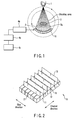
- FIG. 1 shows an X-ray CT apparatus.
- X-rays from an X-ray tube 1 are emitted to form a fan-like X-ray beam with a circular collimator 2.
- the X-ray tube 1, a detector 10 and the circular collimator 2 facing the X-ray tube 1 are rotated around reference to a target object 3.
- the detector 10 obtains X-ray information as a signal from X-rays which have passed through the target object 3.
- An X-ray tomography picture of the target object 3 is obtained by processing the signal by using a computer unit 4b.
- the collimator 2 has a collimator board provided in front of the detector 10.
- the collimator removes the scattered X-rays incident from the oblique directions.
- the collimator passes the X-rays which have traveled straight and penetrated the target object 3.
- the collimator board functions as an X-ray shield wall in front of the detector 10 which is arranged in a one- or two- dimensional manner.
- the detector 10 obtains the X-ray information as a signal from received X-rays which have passed through the target object 3.
- the target object 3 is placed on a couch 3a.
- the X-ray information is sent to a data acquisition system 4a from the detector 10.
- the data obtained from the data acquisition system 4a is sent to a computer unit 4b to display a tomography pictures on a display 4c.
- the computer unit 4b stores and reconstitutes the data.
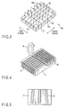
- FIG. 2 is a perspective view to show a detector 10 with a collimator arranged in the one-dimensional manner according to one embodiment of the invention.
- FIG. 3 is a perspective view to show a detector 10 with a collimator arranged in the two- dimensional manner.
- a space between one slot and another slot may be regular or may not be regular.
- laminated X-ray detection elements 11 constituting a part of the detector 10 detect the quantity of the received X-rays.
- the detector 10 is made by alternately adhering slender and square shaped X-ray detection elements 11 and slender square shaped reflectors 17 (reflective material) respectively extending, in a channel direction (a rotating direction of the detector 10) and being arranged adjacently in a slice direction.
- the board-like X-ray shield board (collimator board) 13 is inserted in each of the slots 12.
- a blade 9 is used to process the slots 12.
- X-rays shield boards 13 absorb the X-rays (scatted X-rays) which do not enter straight into the detector 10.
- the X-ray shield boards 13 are disposed so as not to contact the bottom of each of the slots 12 by gap control, as shown in FIG. 8.
- the gap control is carried out so that X-ray shield boards 13 may be inserted so as not to contact the bottoms of the slots.
- a back surface of the laminated elements X-ray detection elements 11 is polished with a scintillator (X-ray detection element) polishing tool as shown in FIG. 8.
- the back surface of the laminated X-rays detection element 11 is not polished with a scintillator polishing tool 9. This is because the X-ray shield boards 13 are made of metal which is hard and may be difficult to polish. The X-ray shield boards 13 are formed except for a polishing area. Therefore, the gap control may not always be necessary, if a polishing tool can polish the laminated elements X-ray detection elements 11 and the X-ray shield boards 13.
- a reflective material 15 serving as an adhesive is applied to the slots 12.
- the reflective material is a gel-like material. By hardening after applying the reflective material, the reflective material works like an adhesive, as shown in FIG. 6.
- the X-ray shield boards 13 are inserted in the slots 12.
- This structure makes it easy to have X-rays reach photo-diodes 6 provided on a back side of the X-ray detection elements 11, as shown in FIG. 10. It is because X-rays reflect by the reflective material 15 in the laminated elements X-ray detection elements 11.
- Scattered X-rays of the channel direction can be absorbed and removed by installing X-rays shield boards to be arranged adjacently in the slice direction perpendicular to the channel direction.
- a plate-like X-ray detection element 21 is used to form X-ray shield boards 23 as well as X-ray shield boards 13a, unlike the laminated X-ray detection element in FIG. 2.
- a comb-like X-ray shield boards 23 are inserted in each of a plurality of slots 22 processed into the plate-like X ray detection element 21 in the perpendicular direction of the slice direction as shown in FIG. 13.
- the X-rays shield boards 13 are inserted in each of the plurality of slots 12a processed into the plate-like X-ray detection element 21 in the shield direction as shown in FIG. 14.
- Reflective material 15a serving as an adhesive is applied to the slots 22 as well as the slots 12a as shown in FIG. 12. After applying the reflective material 15a, the comb-like X-ray shield board 23 is inserted.
- the scattered X-rays in the channel direction may be removed by installing the X-ray shield boards 13a in the direction perpendicular in the channel direction.
- the scattered X-rays in the slice direction may be removed by the comb-like X-ray shield boards 23 installed in the perpendicular direction of the slice direction as shown in FIG. 10.
- the comb-like X-ray shield boards 23 are installed in the perpendicular direction of the slice direction, the X-ray shield boards are not restricted to the comb-like structure or shape. Separate sheet-like X-ray shield boards may be used instead of the comb-like X-ray shield boards 23. Mixture of the separate sheet-like and comb-like X-ray shield boards may be used.
- the board-like X-ray shield boards 13a and the comb-like X-ray shield boards 23 are made of molybdenum (Mo.), because Mo is a high rate material of X-ray interception. However, another material may be used instead of Mo.
- Mo molybdenum
- the detector 20 in FIG. 3 can absorb and intercept not only scattered X-rays of the channel direction but also those of the slice direction, because of honeycomb structure of the detector 20, in comparison with the detector 10 in FIG. 2.
- the detector 20 has a structure which can be bore during a high-speed scanning.
- a positioning process may be omitted to attain reducing a step of manufacturing, to increase accuracy and to improve strength.
Landscapes
- Health & Medical Sciences (AREA)
- Life Sciences & Earth Sciences (AREA)
- Engineering & Computer Science (AREA)
- Physics & Mathematics (AREA)
- High Energy & Nuclear Physics (AREA)
- Medical Informatics (AREA)
- Molecular Biology (AREA)
- Radiology & Medical Imaging (AREA)
- Veterinary Medicine (AREA)
- Nuclear Medicine, Radiotherapy & Molecular Imaging (AREA)
- Optics & Photonics (AREA)
- Pathology (AREA)
- Spectroscopy & Molecular Physics (AREA)
- Biomedical Technology (AREA)
- Heart & Thoracic Surgery (AREA)
- Biophysics (AREA)
- Surgery (AREA)
- Animal Behavior & Ethology (AREA)
- General Health & Medical Sciences (AREA)
- Public Health (AREA)
- Pulmonology (AREA)
- Theoretical Computer Science (AREA)
- General Engineering & Computer Science (AREA)
- General Physics & Mathematics (AREA)
- Apparatus For Radiation Diagnosis (AREA)
- Measurement Of Radiation (AREA)
Abstract
Description
- This invention relates to an X-ray CT(computer tomography) apparatus, an X-ray detector and a method of manufacturing an X-ray detector.
- In an X-ray CT apparatus, X-rays are emitted from an X-ray tube and are formed into a fan-like shaped X-ray beam by a collimator.
- The X-ray tube, and a circular arc like detector and a collimator facing the X-ray tube are rotated around a target object.
- The detector receives X-rays which have passed through the target object and obtains X-ray information as a signal from the received X-ray. An X-ray tomography picture of the target object is obtained by processing the X-ray information by using a computer.
- Some of the X-rays emitted from the X-ray tube travel straight and penetrate the target object, and other X-rays are scattered by the target object.
- The collimator has a collimator board provided in front of the detector. The collimator removes the scattered X-rays incident from the oblique direction. The collimator passes the X-rays which have traveled straight and penetrated the target object.
- The collimator board forms an X-ray shield wall in front of the detector. The detector has detection elements which are arranged in a one- or two-dimensional manner. FIG. 17 and FIG. 18 show perspective views of known collimators and X-ray detectors. FIG. 17 shows a collimator having a collimator board arranged in the one-dimensional manner. FIG. 18 shows a collimator having a collimator board arranged in the two-dimensional manner.
- In FIG. 17,
collimator boards detection element array 52. In FIG. 18, acollimate board 53 is shown together with adetection element array 54. - The collimator arranged in one-dimension removes scattered X-rays in a certain direction, for example, a channel direction.
- The collimator arranged in two dimensions removes scattered X-ray in two directions, for example, channel and slice directions.
- When manufacturing the X-ray detector, a collimator and an X ray detector are needed to be assembled with sufficiently accurate positioning.
- This is because the collimator and the X ray detector are manufactured separately as shown in FIG. 17 or FIG. 18.
- The collimator may contain a plurality of Mo(Molybdenum) boards. The X-ray detector may contain a reflector. In the assembling process, it is necessary to position the collimator and the X-ray detector with a small gap in a rotating direction.
- But it takes considerable time to carry out the assembling process with high positioning accuracy.
- It is an object of the present invention to provide an X-ray CT apparatus positioning which may be manufactured with high positioning accuracy and in a relatively short time. It is another object of the present invention to provide an X-ray detector which may be manufactured with high positioning accuracy and in a relatively short time. It is further another object of the invention to provide a method of manufacturing an X-ray detector with high positioning accuracy and in a relatively short time.
- 1. According to one embodiment of the present invention, an X-ray CT apparatus, is provided, which includes an X-ray tube configured to emit X-rays, a detector faced against the X-ray tube, the detector having a detector element with a plurality of slots and a plurality of a collimator boards inserted into the slots, a data acquisition system configured to receive data detected by the detector, a computer unit configured to reconstitute the data from the data acquisition system and a display configured to show images by the data.
- 2. According to another embodiment of the present invention, an X-ray CT apparatus, is provided, which includes an X-ray tube configured to emit X-rays, a detector faced against the X-ray tube, the detector having a detection element with a plurality of first and second slots, the first slots processed in parallel with a slice direction and formed in a channel direction at a space, the second slots processed in parallel with the channel direction and formed in the slice direction at a space, a reflective and adhesive material filled in the first and second slots, a data acquisition system configured to receive data detected by the detector, a computer unit configured to reconstitute the data from a data acquisition system, a display configured to show images by the data and a plurality of collimator boards inserted into the first and second slots.
- 3. According to another embodiment of the present invention, an X-ray detector, is provided, which includes a detection element having a plurality of slots and a plurality of collimator boards inserted into the slots.
- 4. According to another embodiment of the present invention, an X-ray detector, is provided, which includes a detector element having a plurality of first slots processed in parallel with a slice direction and formed in a channel direction at a space and a plurality of second slots processed in parallel with the channel direction and formed in the slice direction at a space, a reflective and adhesive material filled in the slots and a plurality of collimator boards inserted into the first and second slots.
- 5. According to another embodiment of the present invention, a method of manufacturing X-ray detector, is provided, which includes processing a plurality of slots in a detection element, injecting a reflective and adhesive material into the slots, and inserting a plurality of collimator boards into the slots.
- 6. According to another embodiment of the present invention, a method of manufacturing X-ray detector, is provided, which includes processing a plurality of first slots parallel to a slice direction into the detection element, processing a plurality of second slots parallel to a channel direction into the detection element, injecting a reflective and adhesive material into the first slots parallel to a slice direction, injecting the reflective and adhesive material into the second slots, inserting a plurality of first collimator boards into the first slots, inserting a plurality of first collimator boards into the second slots, and polishing a field opposite to a slot formation side of the detection element.
- The invention can be more fully understood from the following detailed description when taken in conjunction with the accompanying drawings, in which:
- FIG. 1 is a schematic view of one embodiment of an X-ray CT apparatus in accordance with the invention.
- FIG. 2 is a perspective view of one embodiment of a detector in accordance with the invention.
- FIG. 3 is a perspective view of another embodiment of the detector in accordance with the invention.
- FIG. 4 is a perspective view showing slot processing for an embodiment of a detection element in accordance with the invention.
- FIG. 5 is a sectional view showing slot processing of an embodiment of a detection element in accordance with the invention.
- FIG. 6 is a perspective view showing an injecting reflective material serving as adhesive into a detection element of an embodiment in accordance with the invention.
- FIG. 7 is a perspective view showing inserting a collimator board into a detection element of an embodiment in accordance with the invention.
- FIG. 8 is a cross-sectional view showing a collimator board inserted into a detection element of an embodiment in accordance with the invention.
- FIG. 9 is a cross-sectional view showing a polishing position of a detection element of an embodiment in accordance with the invention.
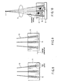
- FIG. 10 is a cross-sectional view showing an X-ray passing route of an embodiment in accordance with the invention.
- FIG. 11 is a perspective view showing slot processing for a detection element of an embodiment in accordance with the invention.
- FIG. 12 is a perspective view showing an injecting reflective material serving as adhesive into a detection element of an embodiment in accordance with the invention.
- FIG. 13 is a cross-sectional view showing inserting a collimator board into a detection element of an embodiment in accordance with the invention.
- FIG. 14 is a perspective view showing a collimator board inserted into a detection element of an embodiment in accordance with the invention.
- FIG. 15 is a cross-sectional view showing polishing position of a detection element of an embodiment in accordance with the invention.
- FIG. 16 is a cross-sectional view showing polishing a detection element of an embodiment of in accordance with the invention.
- FIG. 17 is a perspective view of a conventional collimator and collimator board.
- FIG. 18 is a perspective view of another conventional collimator and collimator board.
- FIG. 1 shows an X-ray CT apparatus. In FIG. 1, X-rays from an X-ray tube 1 are emitted to form a fan-like X-ray beam with a circular collimator 2.
- The X-ray tube 1, a
detector 10 and the circular collimator 2 facing the X-ray tube 1 are rotated around reference to atarget object 3. - The
detector 10 obtains X-ray information as a signal from X-rays which have passed through thetarget object 3. An X-ray tomography picture of thetarget object 3 is obtained by processing the signal by using acomputer unit 4b. - Some of the X-rays emitted from the X-ray tube 1 travel straight and penetrate the
target object 3, and others of the X-rays are scattered by thetarget object 3. - The collimator 2 has a collimator board provided in front of the
detector 10. The collimator removes the scattered X-rays incident from the oblique directions. The collimator passes the X-rays which have traveled straight and penetrated thetarget object 3. - The collimator board functions as an X-ray shield wall in front of the
detector 10 which is arranged in a one- or two- dimensional manner. Thedetector 10 obtains the X-ray information as a signal from received X-rays which have passed through thetarget object 3. Thetarget object 3 is placed on acouch 3a. - The X-ray information is sent to a
data acquisition system 4a from thedetector 10. The data obtained from thedata acquisition system 4a is sent to acomputer unit 4b to display a tomography pictures on adisplay 4c. Thecomputer unit 4b stores and reconstitutes the data. InU.S. Patent No. 6188744 , the entire contents of this reference being incorporated herein by reference. - FIG. 2 is a perspective view to show a
detector 10 with a collimator arranged in the one-dimensional manner according to one embodiment of the invention. - FIG. 3 is a perspective view to show a
detector 10 with a collimator arranged in the two- dimensional manner. A space between one slot and another slot may be regular or may not be regular. - In the embodiment shown in FIG. 2, laminated
X-ray detection elements 11 constituting a part of thedetector 10 detect the quantity of the received X-rays. - The
detector 10 is made by alternately adhering slender and square shapedX-ray detection elements 11 and slender square shaped reflectors 17 (reflective material) respectively extending, in a channel direction (a rotating direction of the detector 10) and being arranged adjacently in a slice direction. - A plurality of
slots 12, which have been processed in the slice direction of the laminatedX-ray detection elements 11, as shown in FIG. 4, are provided in the channel direction. - The board-like X-ray shield board (collimator board) 13 is inserted in each of the
slots 12. In FIG. 4, ablade 9 is used to process theslots 12. -
X-rays shield boards 13 absorb the X-rays (scatted X-rays) which do not enter straight into thedetector 10. - The
X-ray shield boards 13 are disposed so as not to contact the bottom of each of theslots 12 by gap control, as shown in FIG. 8. - The gap control is carried out so that
X-ray shield boards 13 may be inserted so as not to contact the bottoms of the slots. - After inserting the
X-ray shield boards 13, a back surface of the laminated elementsX-ray detection elements 11 is polished with a scintillator (X-ray detection element) polishing tool as shown in FIG. 8. - If the
X-ray shield boards 13 contact the bottoms of theslots 12, the back surface of the laminatedX-rays detection element 11 is not polished with ascintillator polishing tool 9. This is because theX-ray shield boards 13 are made of metal which is hard and may be difficult to polish. TheX-ray shield boards 13 are formed except for a polishing area. Therefore, the gap control may not always be necessary, if a polishing tool can polish the laminated elementsX-ray detection elements 11 and theX-ray shield boards 13. Areflective material 15 serving as an adhesive is applied to theslots 12. The reflective material is a gel-like material. By hardening after applying the reflective material, the reflective material works like an adhesive, as shown in FIG. 6. - Before applying the
reflective material 15 serving as an adhesive and hardening it, theX-ray shield boards 13 are inserted in theslots 12. - It may be unnecessary in this embodiment to carry out positioning of the
reflective boards 15 and theX-ray shield boards 13 as conventional structures. - This is because the
reflective material 15 serving as adhesives and theX-ray shield boards 13 are united as shown in FIG. 7. - This structure makes it easy to have X-rays reach photo-
diodes 6 provided on a back side of theX-ray detection elements 11, as shown in FIG. 10. It is because X-rays reflect by thereflective material 15 in the laminated elementsX-ray detection elements 11. - Scattered X-rays of the channel direction can be absorbed and removed by installing X-rays shield boards to be arranged adjacently in the slice direction perpendicular to the channel direction.
- In FIG. 3, a plate-like
X-ray detection element 21 is used to formX-ray shield boards 23 as well asX-ray shield boards 13a, unlike the laminated X-ray detection element in FIG. 2. - A comb-like
X-ray shield boards 23 are inserted in each of a plurality ofslots 22 processed into the plate-like Xray detection element 21 in the perpendicular direction of the slice direction as shown in FIG. 13. TheX-rays shield boards 13 are inserted in each of the plurality ofslots 12a processed into the plate-likeX-ray detection element 21 in the shield direction as shown in FIG. 14. -
Reflective material 15a serving as an adhesive is applied to theslots 22 as well as theslots 12a as shown in FIG. 12. After applying thereflective material 15a, the comb-likeX-ray shield board 23 is inserted. - It is not always necessary to carry out positioning of reflective boards and the
X-ray shield boards - The scattered X-rays in the channel direction may be removed by installing the
X-ray shield boards 13a in the direction perpendicular in the channel direction. - Further, the scattered X-rays in the slice direction may be removed by the comb-like
X-ray shield boards 23 installed in the perpendicular direction of the slice direction as shown in FIG. 10. - Though, in FIG. 3, the comb-like
X-ray shield boards 23 are installed in the perpendicular direction of the slice direction, the X-ray shield boards are not restricted to the comb-like structure or shape. Separate sheet-like X-ray shield boards may be used instead of the comb-likeX-ray shield boards 23. Mixture of the separate sheet-like and comb-like X-ray shield boards may be used. - The board-like
X-ray shield boards 13a and the comb-likeX-ray shield boards 23 are made of molybdenum (Mo.), because Mo is a high rate material of X-ray interception. However, another material may be used instead of Mo. - With reference to FIG. 4 to FIG. 9, a manufacturing method of the
detector 10 of FIG. 2 will be explained. - (1) In FIG. 4, polishing is performed to the upper surface of a laminated elements
X-ray detection elements 11, to which a reflector (reflective material) 17 is installed in the direction of a channel. The polishing is performed using whetstone or by a polishing machine to formslots 12. - (2) In FIG. 4, the
slot 12 processing is provided to the direction parallel to the slice direction by using theblade 9 as the processing tool. Theslots 12 are formed respectively in the direction toward an X-ray focus. Theslots 12 do not reach the laminated elementsX-ray detection elements 11. For example, it is left about a 0.3 mm depth remains from the undersurface of the laminated elementsX-ray detection elements 11 to theslots 12 as shown in FIG. 4 and FIG. 5.
However, if the undersurface of the laminated elementsX-ray detection elements 11 is fixed with wax, etc. to avoid parting, theslots 12 may reach the undersurface of the laminated elementsX-rays detection elements 11. - (3) The
reflective material 15 serving as an adhesive is injected into theslots 12 as shown in FIG. 6. - (4)
X-ray shield boards 13 are inserted in theslots 12. TheX-ray shield boards 13 are inserted so as not to touch bottoms of theslots 12 as shown in FIG. 7 and FIG. 8. - (5) After the
reflective material 15 is hardened, the undersurface of the laminatedX-ray detection elements 11 are polished to the position where thereflective material 15 can be seen, as shown in FIG. 9. - Referring to FIG. 11 to FIG. 16, the manufacturing method of the detector of FIG. 3 will be explained.
- (1) As shown in FIG. 11, an upper surface of an
X-ray detection element 21 is polished. - (2) The
X-ray detection element 21 is polished in the channel direction and in the slice direction with theblade 9.
Slots 12a andSlots 22 are formed respectively, in the direction toward an X-ray tube focus.
Theslots 12a and theslots 22 do not reach the laminatedX-rays detection elements 11. For example, about a 0.3 mm depth is left from the undersurface of the laminatedX-rays detection elements 11 to theslots 12a as shown in FIG. 11. Theslots 12a is defined as first slots, and theslots 22 is defined as first slots. - (3) A
reflective material 15 is injected into theslots 12a and theslots 22 as shown in FIG. 12. - (4) The comb-like
X-ray shield boards 23 are inserted in theslots 22 after the injection. Then, theX-ray shield boards 13 are inserted into theslots 12a.
TheX-ray shield boards 13 are provided so as not to touch bottoms of theslots 12a and theslots 22 as shown in FIG. 13, to FIG. 15. - (5) After the reflective material is hardened, the undersurfaces of the laminated
X-rays detection element 21 are polished to the position where thereflective material 15 can be seen, as shown in FIG. 16). - The
detector 20 in FIG. 3 can absorb and intercept not only scattered X-rays of the channel direction but also those of the slice direction, because of honeycomb structure of thedetector 20, in comparison with thedetector 10 in FIG. 2. - As a result, the
detector 20 has a structure which can be bore during a high-speed scanning. - Because the
X-ray shield boards 13a and the comb-likeX-ray shield boards 23 are inserted in theX-ray detection elements 21 directly, a positioning process may be omitted to attain reducing a step of manufacturing, to increase accuracy and to improve strength.
Claims (12)
- An X-ray CT apparatus, characterized by comprising:an X-ray tube (1) to emit X-rays;a detector (10) faced against the X-ray tube (1), the detector (10) having a detector element (11) with a plurality of slots (12) and a plurality of a collimator boards (13) inserted into the slots (12);a data acquisition system (4a) configured to receive data detected by the detector (10);a computer unit (4b) configured to reconstitute the data from the data acquisition system (4a); anda display (4c) configured to show images by the data.
- The X-ray CT apparatus according to claim 1, characterized in that a reflective and adhesive material (15) is filled in the slot (12).
- The X-ray CT apparatus according to claim 1, characterized in that the slots (12) are processed in parallel with a slice direction.
- An X-ray CT apparatus, characterized by comprising:an X-ray tube (1) configured to emit X-rays;a detector (20) faced against the X-ray tube, the detector (20) havings a detection element (21) with a plurality of first and second slots (12a, 22), the first slots (12a) processed in parallel with a slice direction and formed in a channel direction at a space, the second slots (22) processed in parallel with the channel direction and formed in the slice direction at a space;a reflective and adhesive material (15a) filled in the first and second slots (12a, 22);a data acquisition system (4a) configured to receive data detected by the detector;a computer unit (4b) configured to reconstitute the data from the data acquisition system (4a); anda display (4c) configured to show images by the data;a plurality of collimator boards (13a, 23) inserted into the first and second slots (12a, 22).
- An X-ray detector, characterized by comprising:a detection element (21) having a plurality of slots (12a, 22) ; anda plurality of collimator boards (13a, 23) inserted into the slots (12a, 22).
- The X-ray detector, according to claim 5, characterized in that a reflective material (15a) with adhesives function is pouring in the slot (12a, 22).
- An X-ray detector according to claim 6, characterized in that the slots (12a) are processed in parallel with a slice direction.
- An X-ray detector, characterized by comprising:a detector element (21) having a plurality of first slots (12a) processed in parallel with a slice direction and formed in a channel direction at a space and a plurality of second slots (22) processed in parallel with the channel direction and formed in the slice direction at a space;a reflective and adhesive material (15a) filled in the slots; anda plurality of collimator boards (13a, 23) inserted into the first and second slots (12a, 22).
- A method of manufacturing X-ray detector characterized by comprising:processing a plurality of slots (12a, 22) in a detection element;injecting a reflective and adhesive material (15) into the slots (12a, 22); andinserting a plurality of collimator boards (13a, 23) into the slots.
- The method of manufacturing an X-ray detector according to claim 9, characterized by further comprising polishing a field is opposite to the slot formation side of the detection element (21) opposite to a slot formation side.
- A method of manufacturing X-ray detector according to claim 9, characterized in that the slot (12a, 22) are processed in a direction of parallel to a slice direction.
- A method of manufacturing in X-ray detector characterized by comprising:processing a plurality of first slots (12a) parallel to a slice direction into the detection element (21);processing a plurality of second slots (22) parallel to a channel direction into the detection element (21);injecting a reflective and adhesive material (15a) into the first slots (12a) parallel to a slice direction;injecting the reflective and adhesive material (15a) the second slots (22);inserting a plurality of first collimator boards (13a) into the first slots;inserting a plurality of first collimator boards (23) into the second slots; andpolishing a field opposite to a slot formation side of the detection element (21).
Applications Claiming Priority (1)
| Application Number | Priority Date | Filing Date | Title |
|---|---|---|---|
| JP2005276726A JP4718949B2 (en) | 2005-09-22 | 2005-09-22 | X-ray CT apparatus and X-ray CT apparatus manufacturing method |
Publications (2)
| Publication Number | Publication Date |
|---|---|
| EP1767151A1 true EP1767151A1 (en) | 2007-03-28 |
| EP1767151B1 EP1767151B1 (en) | 2011-01-19 |
Family
ID=37561120
Family Applications (1)
| Application Number | Title | Priority Date | Filing Date |
|---|---|---|---|
| EP06019770A Not-in-force EP1767151B1 (en) | 2005-09-22 | 2006-09-21 | X-ray CT apparatus, x-ray detector and method of manufacturing x-ray detector |
Country Status (4)
| Country | Link |
|---|---|
| US (1) | US7397888B2 (en) |
| EP (1) | EP1767151B1 (en) |
| JP (1) | JP4718949B2 (en) |
| CN (1) | CN1936557B (en) |
Families Citing this family (12)
| Publication number | Priority date | Publication date | Assignee | Title |
|---|---|---|---|---|
| DE102008063310B3 (en) * | 2008-12-30 | 2010-04-15 | Siemens Aktiengesellschaft | Radiation detector module manufacturing method for use in computer tomography, involves connecting conversion element with radiation entrance surface with collimator element, and perpendicularly aligning collimator element to surface |
| DE102010020610A1 (en) * | 2010-05-14 | 2011-11-17 | Siemens Aktiengesellschaft | Radiation detector and method for producing a radiation detector |
| CN102971644B (en) * | 2010-09-14 | 2016-03-16 | 株式会社东芝 | Mo collimating apparatus and use the X-ray detector of this Mo collimating apparatus, X ray checking device and CT device |
| US20120087462A1 (en) * | 2010-10-12 | 2012-04-12 | Abdelaziz Ikhlef | Hybrid collimator for x-rays and method of making same |
| JP2013068435A (en) * | 2011-09-20 | 2013-04-18 | Toshiba Corp | Collimator, manufacturing method of collimator and x-ray ct apparatus |
| DE102011083422B4 (en) * | 2011-09-26 | 2017-08-10 | Siemens Healthcare Gmbh | Method for producing a collimator |
| JP2013186010A (en) * | 2012-03-08 | 2013-09-19 | Toshiba Corp | Manufacturing method of collimator, collimator, and x-ray ct apparatus |
| DE102012206546B4 (en) * | 2012-04-20 | 2019-06-27 | Siemens Healthcare Gmbh | Method for producing a scattered radiation grid and scattered grid of a CT detector |
| US8890079B2 (en) * | 2012-06-29 | 2014-11-18 | General Electric Company | Radiation detection device and radiation tomographic apparatus, and method for assembling radiation detection device |
| US10178980B2 (en) * | 2014-06-19 | 2019-01-15 | Analogic Corporation | Radiation sources and detector array for imaging modality |
| WO2018208300A1 (en) * | 2017-05-11 | 2018-11-15 | Analogic Corporation | Anti-scatter collimator for radiation imaging modalities |
| CN109273131B (en) * | 2018-10-31 | 2024-07-02 | 同方威视技术股份有限公司 | Collimator assembly and radiation detection device |
Citations (6)
| Publication number | Priority date | Publication date | Assignee | Title |
|---|---|---|---|---|
| US4982096A (en) * | 1988-01-06 | 1991-01-01 | Hitachi Medical Corporation | Multi-element radiation detector |
| JPH042989A (en) * | 1990-04-20 | 1992-01-07 | Toshiba Corp | Manufacture of detector for x-ray ct apparatus |
| DE19923372A1 (en) * | 1999-05-21 | 2000-07-13 | Siemens Ag | Computer tomography radiation detector manufacturing method |
| US6553092B1 (en) * | 2000-03-07 | 2003-04-22 | Koninklijke Philips Electronics, N.V. | Multi-layer x-ray detector for diagnostic imaging |
| US6707884B1 (en) * | 1999-03-19 | 2004-03-16 | Fuji Photo Film Co., Ltd. | X-ray scatter reducing grid and fabrication method thereof |
| WO2006016341A1 (en) * | 2004-08-10 | 2006-02-16 | Philips Intellectual Property & Standards Gmbh | Arrangement of a scintillator and an anti-scatter-grid |
Family Cites Families (8)
| Publication number | Priority date | Publication date | Assignee | Title |
|---|---|---|---|---|
| JPS60236632A (en) * | 1984-05-10 | 1985-11-25 | 株式会社東芝 | Fourth generation ct apparatus |
| JPH1189827A (en) | 1997-09-19 | 1999-04-06 | Toshiba Corp | X-ray computed tomography apparatus |
| JPH11133155A (en) * | 1997-10-27 | 1999-05-21 | Hitachi Medical Corp | X-ray detector and x-ray ct device |
| US6188744B1 (en) | 1998-03-30 | 2001-02-13 | Kabushiki Kaisha Toshiba | X-ray CT apparatus |
| JP2000316841A (en) * | 1999-05-11 | 2000-11-21 | Hitachi Medical Corp | Multi-slice x-ray ct apparatus |
| JP2001027673A (en) * | 1999-07-15 | 2001-01-30 | Hitachi Medical Corp | X-ray detector and x-ray ct apparatus using the same |
| JP2002207082A (en) | 2001-01-09 | 2002-07-26 | Shimadzu Corp | Two-dimensional radiation detector and manufacturing method thereof |
| JP4309631B2 (en) * | 2001-10-22 | 2009-08-05 | 株式会社東芝 | X-ray computer tomography equipment |
-
2005
- 2005-09-22 JP JP2005276726A patent/JP4718949B2/en not_active Expired - Fee Related
-
2006
- 2006-09-21 EP EP06019770A patent/EP1767151B1/en not_active Not-in-force
- 2006-09-21 US US11/524,251 patent/US7397888B2/en not_active Expired - Fee Related
- 2006-09-22 CN CN2006101598060A patent/CN1936557B/en not_active Expired - Fee Related
Patent Citations (6)
| Publication number | Priority date | Publication date | Assignee | Title |
|---|---|---|---|---|
| US4982096A (en) * | 1988-01-06 | 1991-01-01 | Hitachi Medical Corporation | Multi-element radiation detector |
| JPH042989A (en) * | 1990-04-20 | 1992-01-07 | Toshiba Corp | Manufacture of detector for x-ray ct apparatus |
| US6707884B1 (en) * | 1999-03-19 | 2004-03-16 | Fuji Photo Film Co., Ltd. | X-ray scatter reducing grid and fabrication method thereof |
| DE19923372A1 (en) * | 1999-05-21 | 2000-07-13 | Siemens Ag | Computer tomography radiation detector manufacturing method |
| US6553092B1 (en) * | 2000-03-07 | 2003-04-22 | Koninklijke Philips Electronics, N.V. | Multi-layer x-ray detector for diagnostic imaging |
| WO2006016341A1 (en) * | 2004-08-10 | 2006-02-16 | Philips Intellectual Property & Standards Gmbh | Arrangement of a scintillator and an anti-scatter-grid |
Also Published As
| Publication number | Publication date |
|---|---|
| JP4718949B2 (en) | 2011-07-06 |
| CN1936557A (en) | 2007-03-28 |
| CN1936557B (en) | 2010-04-14 |
| US7397888B2 (en) | 2008-07-08 |
| US20070071163A1 (en) | 2007-03-29 |
| JP2007082844A (en) | 2007-04-05 |
| EP1767151B1 (en) | 2011-01-19 |
Similar Documents
| Publication | Publication Date | Title |
|---|---|---|
| US7397888B2 (en) | X-ray CT apparatus, X-ray detector and method of manufacturing X-ray detector | |
| US8451977B2 (en) | Collimator module, X-ray detector, X-ray CT device, and assembling method of collimator module | |
| US6271524B1 (en) | Gamma ray collimator | |
| US9020093B2 (en) | Two-dimensional collimator module, X-ray detector, X-ray CT apparatus, and method for assembling two-dimensional collimator module | |
| JP4558372B2 (en) | Collimator assembly with multiple components | |
| JP5443736B2 (en) | Radiation detector and X-ray CT apparatus | |
| US20080165922A1 (en) | Laminated ct collimator and method of making same | |
| EP1996077B1 (en) | Dual-source scanning-based detection of ionizing radiation | |
| JP2001194463A (en) | Grid for absorbing X-rays | |
| CN101644687A (en) | Method and device for ray bundle scanning for back scattering imaging | |
| US6881960B2 (en) | Thick scintillation plate with internal light collimation | |
| JP2013029495A (en) | Methods and apparatus for collimation of detector | |
| US20100158195A1 (en) | Method for producing a comb-like collimator element for a collimator arrangement and collimator element | |
| CN110430815B (en) | Anti-scatter collimator for radiation imaging modes | |
| US9864073B1 (en) | Systems and methods for controlling optical coupling between scintillator crystals | |
| US8476610B2 (en) | Composite segment collimators for SPECT without dead zones | |
| JP3730319B2 (en) | X-ray computed tomography system | |
| CN101443856A (en) | Grid for selective absorption of electromagnetic radiation and method for its manufacture | |
| JP2002236182A (en) | Method for manufacturing one-dimensional or multi-dimensional detector array | |
| JP4817524B2 (en) | X-ray solid state detector manufacturing method | |
| US9612344B2 (en) | Positron emission tomography and single photon emission computed tomography based on intensity attenuation shadowing methods and effects | |
| JP2002207082A (en) | Two-dimensional radiation detector and manufacturing method thereof | |
| WO2004051312A1 (en) | Radiation detector and medical image diagnosing device | |
| CN100592079C (en) | Collimator for X-ray CT apparatus and manufacturing method thereof | |
| Kurfess et al. | Coincident Compton nuclear medical imager |
Legal Events
| Date | Code | Title | Description |
|---|---|---|---|
| PUAI | Public reference made under article 153(3) epc to a published international application that has entered the european phase |
Free format text: ORIGINAL CODE: 0009012 |
|
| 17P | Request for examination filed |
Effective date: 20060921 |
|
| AK | Designated contracting states |
Kind code of ref document: A1 Designated state(s): AT BE BG CH CY CZ DE DK EE ES FI FR GB GR HU IE IS IT LI LT LU LV MC NL PL PT RO SE SI SK TR |
|
| AX | Request for extension of the european patent |
Extension state: AL BA HR MK YU |
|
| 17Q | First examination report despatched |
Effective date: 20070620 |
|
| AKX | Designation fees paid |
Designated state(s): FR NL |
|
| REG | Reference to a national code |
Ref country code: DE Ref legal event code: 8566 |
|
| GRAP | Despatch of communication of intention to grant a patent |
Free format text: ORIGINAL CODE: EPIDOSNIGR1 |
|
| GRAS | Grant fee paid |
Free format text: ORIGINAL CODE: EPIDOSNIGR3 |
|
| GRAA | (expected) grant |
Free format text: ORIGINAL CODE: 0009210 |
|
| AK | Designated contracting states |
Kind code of ref document: B1 Designated state(s): FR NL |
|
| REG | Reference to a national code |
Ref country code: NL Ref legal event code: T3 |
|
| PLBE | No opposition filed within time limit |
Free format text: ORIGINAL CODE: 0009261 |
|
| STAA | Information on the status of an ep patent application or granted ep patent |
Free format text: STATUS: NO OPPOSITION FILED WITHIN TIME LIMIT |
|
| 26N | No opposition filed |
Effective date: 20111020 |
|
| REG | Reference to a national code |
Ref country code: FR Ref legal event code: PLFP Year of fee payment: 10 |
|
| PGFP | Annual fee paid to national office [announced via postgrant information from national office to epo] |
Ref country code: FR Payment date: 20150629 Year of fee payment: 10 |
|
| PGFP | Annual fee paid to national office [announced via postgrant information from national office to epo] |
Ref country code: NL Payment date: 20150909 Year of fee payment: 10 |
|
| REG | Reference to a national code |
Ref country code: NL Ref legal event code: MM Effective date: 20161001 |
|
| PG25 | Lapsed in a contracting state [announced via postgrant information from national office to epo] |
Ref country code: NL Free format text: LAPSE BECAUSE OF NON-PAYMENT OF DUE FEES Effective date: 20161001 |
|
| REG | Reference to a national code |
Ref country code: FR Ref legal event code: ST Effective date: 20170531 |
|
| PG25 | Lapsed in a contracting state [announced via postgrant information from national office to epo] |
Ref country code: FR Free format text: LAPSE BECAUSE OF NON-PAYMENT OF DUE FEES Effective date: 20160930 |