EP1764403A2 - Fluorescent material,fluorescent substance, display, and process for preparing fluorescent substance - Google Patents
Fluorescent material,fluorescent substance, display, and process for preparing fluorescent substance Download PDFInfo
- Publication number
- EP1764403A2 EP1764403A2 EP06018649A EP06018649A EP1764403A2 EP 1764403 A2 EP1764403 A2 EP 1764403A2 EP 06018649 A EP06018649 A EP 06018649A EP 06018649 A EP06018649 A EP 06018649A EP 1764403 A2 EP1764403 A2 EP 1764403A2
- Authority
- EP
- European Patent Office
- Prior art keywords
- fluorescent
- fluorescent substance
- layer
- fluorescent material
- comprised
- Prior art date
- Legal status (The legal status is an assumption and is not a legal conclusion. Google has not performed a legal analysis and makes no representation as to the accuracy of the status listed.)
- Withdrawn
Links
Images



Classifications
-
- H—ELECTRICITY
- H01—ELECTRIC ELEMENTS
- H01J—ELECTRIC DISCHARGE TUBES OR DISCHARGE LAMPS
- H01J29/00—Details of cathode-ray tubes or of electron-beam tubes of the types covered by group H01J31/00
- H01J29/02—Electrodes; Screens; Mounting, supporting, spacing or insulating thereof
- H01J29/10—Screens on or from which an image or pattern is formed, picked up, converted or stored
- H01J29/18—Luminescent screens
- H01J29/20—Luminescent screens characterised by the luminescent material
-
- C—CHEMISTRY; METALLURGY
- C09—DYES; PAINTS; POLISHES; NATURAL RESINS; ADHESIVES; COMPOSITIONS NOT OTHERWISE PROVIDED FOR; APPLICATIONS OF MATERIALS NOT OTHERWISE PROVIDED FOR
- C09K—MATERIALS FOR MISCELLANEOUS APPLICATIONS, NOT PROVIDED FOR ELSEWHERE
- C09K11/00—Luminescent materials, e.g. electroluminescent or chemiluminescent
- C09K11/08—Luminescent materials, e.g. electroluminescent or chemiluminescent containing inorganic luminescent materials
- C09K11/77—Luminescent materials, e.g. electroluminescent or chemiluminescent containing inorganic luminescent materials containing rare earth metals
- C09K11/7728—Luminescent materials, e.g. electroluminescent or chemiluminescent containing inorganic luminescent materials containing rare earth metals containing europium
- C09K11/77342—Silicates
-
- H—ELECTRICITY
- H01—ELECTRIC ELEMENTS
- H01J—ELECTRIC DISCHARGE TUBES OR DISCHARGE LAMPS
- H01J29/00—Details of cathode-ray tubes or of electron-beam tubes of the types covered by group H01J31/00
- H01J29/02—Electrodes; Screens; Mounting, supporting, spacing or insulating thereof
- H01J29/10—Screens on or from which an image or pattern is formed, picked up, converted or stored
- H01J29/18—Luminescent screens
- H01J29/24—Supports for luminescent material
-
- H—ELECTRICITY
- H01—ELECTRIC ELEMENTS
- H01J—ELECTRIC DISCHARGE TUBES OR DISCHARGE LAMPS
- H01J31/00—Cathode ray tubes; Electron beam tubes
- H01J31/08—Cathode ray tubes; Electron beam tubes having a screen on or from which an image or pattern is formed, picked up, converted, or stored
- H01J31/10—Image or pattern display tubes, i.e. having electrical input and optical output; Flying-spot tubes for scanning purposes
- H01J31/12—Image or pattern display tubes, i.e. having electrical input and optical output; Flying-spot tubes for scanning purposes with luminescent screen
- H01J31/123—Flat display tubes
- H01J31/125—Flat display tubes provided with control means permitting the electron beam to reach selected parts of the screen, e.g. digital selection
- H01J31/127—Flat display tubes provided with control means permitting the electron beam to reach selected parts of the screen, e.g. digital selection using large area or array sources, i.e. essentially a source for each pixel group
-
- Y—GENERAL TAGGING OF NEW TECHNOLOGICAL DEVELOPMENTS; GENERAL TAGGING OF CROSS-SECTIONAL TECHNOLOGIES SPANNING OVER SEVERAL SECTIONS OF THE IPC; TECHNICAL SUBJECTS COVERED BY FORMER USPC CROSS-REFERENCE ART COLLECTIONS [XRACs] AND DIGESTS
- Y10—TECHNICAL SUBJECTS COVERED BY FORMER USPC
- Y10T—TECHNICAL SUBJECTS COVERED BY FORMER US CLASSIFICATION
- Y10T428/00—Stock material or miscellaneous articles
- Y10T428/24—Structurally defined web or sheet [e.g., overall dimension, etc.]
- Y10T428/24628—Nonplanar uniform thickness material
Definitions
- the present invention relates to a fluorescent material, a fluorescent substance and a process for preparing the same, and a display using the fluorescent substance.
- Preparation of a fluorescent layer having a light-emitting function and a process for synthesizing fluorescent substance powder are important technologies for realizing light emitting devices or display devices.
- fluorescent layers for cathode ray tubes (CRTs), plasma display panels (PDPs) or field emission displays (FEDs) are prepared by powder firing method.
- fluorescent layers for electroluminescence displays (ELDs) are prepared using a physical vapor deposition method such as electron beam deposition resistance heating deposition or sputtering, or a chemical vapor deposition method such as chemical vapor deposition, sol-gel deposition or chemical solution deposition.
- fluorescent substances are required to give full color light, and thus, fluorescent substances of three primary colors - red, green and blue which excel in luminous efficiency, color purity, stability and emission response are being developed energetically.
- fluorescent substances for CRTs or FEDs which are excited by electron beam
- sulfides are in use which have undergone surface treatment with a silicate compound to improve their lifetime.
- the electron beam irradiation time is longer than that of fluorescent substances for CRTs, whereby their deterioration is accelerated.
- fluorescent substances for PDPs which are excited by UV light, an oxide or an oxysulfide containing sulfur as its part is in use.
- a blue fluorescent substance BaMgAl 10 O 17 :Eu 2+ (BAM) for PDPs presents a problem of deterioration by moisture adsorption etc. at portions where bonding force is weak due to its crystalline structure, that is, at Ba-O layers between spinel layers in ⁇ -alumina structure.
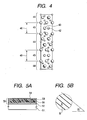
- the distance 46 between the spinel layers between which a Ba-O layer 45 comprised of barium 42 and oxygen 43 lies, as shown in FIG. 4 is about 0.30 nm, which is larger than the size of water molecule, about 0.26 nm. This causes the adsorption of water molecules on the rare earth ions, which are replaced for part of barium 42 in the crystal, subsequently leading to deterioration by moisture.
- Diopside has a crystal structure where SiO 4 tetrahedrons 11 bond with each other at their two corners to form a chain-like shape, as shown in FIG. 2, and divalent metal ions 12 are packed in the chain-like portions, as shown in FIG. 3, and is known as representative of chain silicate compounds.
- CaMgSi 2 O 6 :Eu 2+ (CMS) Japanese Patent Application Laid-Open No. 2005-23306 ), which has lately attracted considerable attention as an alternative material to BAM, is considered to be less likely to suffer significant deterioration because it has the diopside crystal structure.
- the distance 33 between the two adjacent chains of SiO 4 tetrahedrons of the diopside crystal structure is about 0.30 nm, which is larger than the size of water molecule, about 0.26 nm.
- the principal object of the present invention is to provide a novel oxide fluorescent material which has good resistance to external environmental factors such as water and suffers less temperature quenching, and moreover, to provide a display using the fluorescent material.
- a fluorescent material comprising an element selected from the group consisting of Mg, Ca, Sr and Ba; an element selected from the group consisting of Si and Ge; an element selected from the group consisting of rare earth elements; and oxygen and having a pseudowollastonite crystal structure.
- a fluorescent substance comprising a portion comprised of the above fluorescent material; and an adjacent layer which is comprised of an element selected from the group consisting of Si and Ge and is in contact with the portion.
- the interface of the portion comprised of the fluorescent material and the adjacent layer preferably has a curved shape on a cycle 0.1 to 1 ⁇ m.
- a fluorescent substance comprising a layer comprised of the above fluorescent material and a layer comprised of an element selected from the group consisting of Si and Ge, the layers stacked on a substrate.
- a display comprising the above fluorescent substanc and a means of exciting the fluorescent substance.
- a process for preparing a fluorescent substance comprising the steps of preparing a precursor by providing a first member which is comprised of an element selected from the group consisting of Mg, Ca, Sr and Ba, a rare earth element, an element selected from the group consisting of Si and Ge, and oxygen and a second member which is comprised of Si or Ge and arranging the second member adjacent to the first member and heat-treating the precursor in a reduced atmosphere.
- the precursor preferably comprises a layer comprised of the first member and a layer comprised of the second member, the layers stacked on a substrate.
- a display comprising an oxide fluorescent substance that has a crystal structure of pseudowollastonite; and a means of exciting the oxide fluorescent substance.
- the present invention it is possible to provide a novel oxide fluorescent material which has good resistance to external environmental factors such as water and suffers less temperature quenching, and moreover, to provide a display using the fluorescent material.
- FIG. 1 is a view showing the crystal structure of pseudowollastonite of the present invention, as seen across the a-axis of the crystal.
- FIG. 2 is a view showing the crystal structure of diopside which is used for comparison with the present invention.
- FIG. 3 is a view of the crystal structure of diopside, as seen across the b-axis of the crystal.
- FIG. 4 is a view of the crystal structure of ⁇ -alumina, as seen across the a-axis of the crystal.
- FIG. 5A is a sectional view of a fluorescent substance prepared in accordance with the present invention and FIG. 5B is an enlarged partial sectional view of the same.
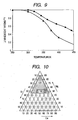
- FIG. 6 is a graph showing the excitation and emission spectra of the fluorescent substance of the present invention.
- FIGS. 7A and 7B are sectional views of a fluorescent substance of the present invention before and after heat treatment, respectively.
- FIG. 8 is a view of a display of the present invention.
- FIG. 9 is a graph showing the dependency of the emission intensity of a fluorescent substance of the present invention on temperature.
- FIG. 10 is a triangular diagram showing the compositional range for Mg, Ca and Sr of the fluorescent material of the present invention.
- the pseudowollastonite has a crystal structure characterized in that it includes SiO 4 tetrahedrons 11 each three of which are linked together to take the form of a three-membered ring 21 and divalent metal ions which bond the SiO 4 tetrahedrons 11 in the form of a three-membered ring together, as shown in American Mineralogist, Volume 84, pages 929-932 or in FIG. 1.
- the distance 13 between the three-membered ring layers is about 0.22 nm, which is small than the size of water molecule, about 0.26 nm. This makes it hard to cause the adsorption of water molecules on the rare earth ions, which are replaced for part of divalent metal ions 12, and hence deterioration by moisture.
- the fluorescent material of the present invention is a novel fluorescent material prepared by adding an activator of a rare earth element to a base material having a pseudowollastonite crystal structure.
- Use of a fluorescent material having the crystal structure of the present invention makes it possible to decrease the dependency of luminescence or luminous efficiency on temperature.
- Silicate compounds having a pseudowollastonite crystal structure are generally expressed by the chemical formula XYO 3 (X, Y each represent an element), as is represented by CaSiO 3 .
- the composition ratio of X, Y, O in the pseudowollastonite crystal structure that constitutes the fluorescent material of the present invention is not limited to 1 : 1 : 3.
- the composition ratio of X, Y, O in the fluorescent material of the present invention is not specifically limited one as long as the crystal structure that constitutes the fluorescent material is a pseudowollastonite crystal structure.
- the fluorescent material of the present invention is an oxide of (Mg x , Ca y , Sr z , Eu w )(Si 1-a Ge a ), that is, (Mg x , Ca y , Sr z , Eu w ) (Si 1-a Ge a )O v wherein the composition of Mg, Ca and Sr is such that 0.45 ⁇ x, 0.05 ⁇ y ⁇ 0.5 and 0.05 ⁇ z ⁇ 0.5, as shown by the triangle 101 in the triangular diagram of FIG. 10, and 0 ⁇ w ⁇ 0.4 and 0 ⁇ a ⁇ 1.
- the fluorescent material includes oxygen atom O in such a rate that satisfies the following expression: 2.5 ⁇ v ⁇ 3.5.
- the fluorescent material of the present invention exhibits excellent crystallinity when it is formed into a fluorescent thin layer of fluorescent substance on a substrate.
- the fluorescent material of the present invention makes it possible to obtain a fluorescent thin layer exhibiting excellent crystallinity, thereby improving the luminance and color purity of the fluorescent substance and the stability of fluorescent thin layer.
- the fluorescent material of the present invention can be synthesized in powder by using MgCO 3 , SrCO 3 , CaCO 3 , MgCl 2 , SrCl 2 , CaCl 2 , Eu 2 O 3 , EuCl 3 , SiO 2 or GeO 2 as starting materials and mixing and firing the same.
- the fluorescent substance of the present invention can be formed as a thin layer (hereinafter referred to as "fluorescent thin layer") on a substrate of, for example, Si, Ge, alumina, quartz or SrTiO 3 .
- an adjacent layer 52 which includes Si and/or Ge, is provided in such a manner as to allow it to come in contact with the fluorescent thin layer 54, as shown in FIG. 5A, the composition deviation among the components Si, Ge and oxygen included in the fluorescent material is less likely to occur, whereby a fluorescent substance having excellent stability against environmental factors such as temperature and humidity can be obtained.
- fluorescent substance used for the present invention means a fluorescent substance including a fluorescent thin layer and optionally an adjacent layer.
- SiO 2 , GeO 2 , SiN x or SiO x N y can be used as materials for the adjacent layer.
- the thickness of the adjacent layer is equal to or larger than the thickness of the portion comprised of a fluorescent material.
- the thickness is, for example, 10 nm to 1 ⁇ m.
- the interface of the fluorescent thin layer and the adjacent layer has a curved surface on a cycle 0.1 to 1 ⁇ m.
- the reason is that the interface having a shape that changes on a cycle almost the same as the wavelength of the fluorescence in the visible range, about 0.1 to 1 ⁇ m, emitted in the inside of the fluorescent material of the present invention can scatter the emitted fluorescence effectively, whereby the fluorescent substance can emit the fluorescence outside effectively.
- the fluorescent material of the present invention can be synthesized in powder by using MgCO 3 , SrCO 3 , CaCO 3 , MgCl 2 , SrCl 2 , CaCl 2 , Eu 2 O 3 , EuCl 3 , SiO 2 or GeO 2 as starting materials and mixing and firing the same.
- the fluorescent material of the present invention can be formed as a thin layer on a substrate of, for example, Si, Ge, alumina, quartz or SrTiO 3 .
- a various types of layer forming means such as sol-gel deposition, vacuum deposition or chemical vapor deposition can be used; however, preferably sputtering is used which can provide a close and excellently reproductive layer relatively easily.
- One example of preferred processes for preparing a fluorescent substance of the present invention is a process that includes: a step of preparing a precursor, which is comprised of a substrate, an adjacent layer and a fluorescent thin layer, by providing a first member that includes, as constituting elements, at least one element selected from the group consisting of Mg, Ca, Sr and Ba, at least one element selected from the group consisting of rare earth elements, at least one element selected from the group consisting of Si and Ge, and oxygen adjacent to a second member that includes Si or Ge as a main component; and a step of heat-treating the precursor in a reduced atmosphere.
- a substrate 51 having a layer 52 which includes Si or Ge, as a second member is prepared.
- Any one of various types of substrates comprised of, for example, alumina, quartz or SrTiO 3 can be used.
- the substrate may be a Si substrate with SiO 2 obtained by forming a thermal oxide layer in any thickness on a Si substrate or a quartz substrate may be used.
- a substrate on which a layer of SiO 2 or GeO 2 is formed can also be used.
- a thin layer 53 comprised of the first member which includes, as constituting elements, at least one element selected from the group consisting of Mg, Ca, Sr and Ba, at least one element selected from the group consisting of rare earth elements, at least one element selected from the group consisting of Si and Ge, and oxygen, is formed so that a precursor 71 comprised of the thin layer 53, the adjacent layer 52 and the substrate 51 is formed (FIG. 7A).
- a various types of layer forming means such as sol-gel deposition, vacuum deposition or chemical vapor deposition can be used; however, preferably sputtering is used which can provide a close and excellently reproductive layer relatively easily.
- the precursor 71 is subjected to heat treatment in a reduced atmosphere so that its crystallinity is improved and the activator added is activate.
- reduced atmospheres include: atmospheres of an inert gas such as N 2 , Ar or He, hydrogen gas, carbon monoxide gas, or a mixed gas of hydrogen or carbon monoxide with N 2 , Ar or He; and a vacuum atmosphere.
- an inert gas such as N 2 , Ar or He
- a vacuum atmosphere preferably a mixed gas of Ar or He that contains several % of H 2 is used.
- the heat treatment temperature is in the range of, for example, 600°C to 1400°C, though it depends on the composition of the materials used or the atmosphere in which the treatment is conducted.
- the heat treatment causes diffusion of substances between the thin layer 53 and the adjacent layer 52, whereby a fluorescent thin layer 54 having excellent crystallinity can be formed.
- a fluorescent structure 72 which includes a fluorescent substance 59 comprised of the fluorescent thin layer 54 and the adjacent layer 52 on the substrate 51.
- the adjacent layer 52 contains a Si or Ge composition (e.g. SiO 2 , GeO 2 ) which is also contained in the fluorescent thin layer 54, the fluorescent thin layer 54 can be preferably prepared by an easy process in a stable manner while avoiding the effect of the composition deviation in the thin layer.
- the thickness of the thin layer 53 prepared in advance is equal to or larger than the thickness of the fluorescent thin layer 54.
- the identification of the material composition and crystal structure can be made by X-ray diffraction analysis, X-ray fluorescence analysis, energy-dispersive spectrometry, inductively coupled plasma emission spectrometry, or transmission electron microscopy.
- the fluorescent substance of the present invention is applicable to FEDs using electron beam excitation, PDPs using UV light excitation, light emitting devices such as EL, image displays, lighting systems or printing systems.
- silicate fluorescent substance characterized in that it was composed of Mg, Ca, Sr, Si, O, as constituting elements, it included a rare earth element, as an activator, and its crystal structure was that of pseudowollastonite.
- a magnetron sputtering system mounted with 3 cathodes was used for the layer formation.
- the thin layer 53 about 500 nm thick was formed by using 3 targets MgSiO 3 , CaSiO 3 and SrSiO 3 each having about 2% of Eu 2 O 3 added and supplying 200 W of RF power to each target so that a precursor 71 was obtained.
- the temperature of the substrate 51 was 200°C
- the pressure in the chamber was kept at about 1 Pa by flowing the mixed gas of argon and oxygen in the chamber, and the deposition rate was about 3 nm/min.
- the precursor 71 was heat treated at about 1000°C in an Ar atmosphere containing 2% of H 2 using a vacuum annealing system to obtain a fluorescent structure 72 including a fluorescent substance 59 comprised of a fluorescent thin layer 54 and an adjacent layer 52 on the substrate 51 (FIG. 7B).
- the fluorescent thin layer 54 had a pseudowollastonite crystal structure where the metal atoms (Mg, Sr, Ca) and the SiO 4 three-membered ring were alternately stacked.
- the heat treatment step substance diffusion was caused between the thin layer 53 and the adjacent layer 52, whereby the interface 55 of the fluorescent thin layer and the adjacent layer had a curved surface on a cycle 0.1 to 1 ⁇ m.
- the heat treatment utilizing this substance diffusion made possible the preparation of a fluorescent substance 59 which suffered less composition fluctuation, had fewer grain boundaries or defects, and hence an excellent crystallinity. This improved the luminance, color purity and stability of the fluorescent thin layer. Furthermore, the resultant fluorescent thin layer showed excellent characteristics in dependency of light emission caused by UV light irradiation on temperature.
- the fluorescent substance 59 had some other structural characteristics. One of the characteristics was that the angle e between the stacked crystal face and the substrate surface was fixed, for example, 40°. It was also found that the fluorescent thin layer 54 had vacant spaces 56 (portions having lower density) about 1 ⁇ m 3 in size in it inside. It is assumed that these characteristic thin layer structure (the curved shape of the interface, the angle between the crystal face and the substrate surface, vacant spaces) makes it possible to effectively take out the light emitted in the inside of the fluorescent material outside. That is, it is assumed that excellent external quantum efficiency can be obtained by such a structure.
- a fluorescent thin layer 54 including Mg, Ca, Sr, Eu, Si and O as constituting elements was prepared on a single crystal substrate or a ceramic substrate.
- a sapphire single crystal substrate was used as a substrate 51.
- a SiO 2 thin layer about 500 nm thick was formed as an adjacent layer 52 on the substrate 51.
- Layer formation was performed by magnetron sputtering using a SiO 2 target.
- the substrate temperature was 200°C or lower, the pressure in the chamber was kept at 0.5 Pa by flowing argon gas in the chamber, and the deposition rate was 6 nm/min.
- a thin layer 53 which includes Mg, Ca, Sr, Eu, Si and O as constituting elements.
- a magnetron sputtering system mounted with 3 cathodes was used for the layer formation.
- the thin layer 53 about 500 nm thick was formed by using 3 targets MgSiO 3 , CaSiO 3 and SrSiO 3 each having about 5% of Eu 2 O 3 added and supplying 180 W, 200 W and 200 W of RF power to the respective targets while keeping the substrate temperature at 100°C, the pressure in the chamber at about 1 Pa by flowing a mixed gas of argon and oxygen, and deposition rate at 3 nm/min so that a precursor 71 was obtained (FIG. 7A).
- the precursor 71 was heat treated at about 1000°C in a He atmosphere containing 3% of H 2 using a vacuum annealing system to obtain a fluorescent structure 72 including a fluorescent substance 59 comprised of a fluorescent thin layer 54 and an adjacent layer 52 on the substrate 51 (FIG. 7B).
- the process of this example makes possible the preparation of a fluorescent substance on a SrTiO 3 single crystal substrate or a fired BaTiO 3 ceramic substrate. This allows a fluorescent substance to find wider application.
- a fluorescent thin layer including Mg, Ca, Sr, Eu, Si, Ge and O as constituting elements was prepared.
- a sapphire single crystal substrate was used as a substrate 51.
- a GeO 2 thin layer about 500 nm thick was formed as an adjacent layer 52.
- Layer formation was performed by magnetron sputtering using a GeO 2 target.
- the substrate temperature was 100°C
- the pressure in the chamber was kept at 0.5 Pa by flowing argon gas in the chamber, and the deposition rate was 5 nm/min.
- a thin layer 53 which includes Mg, Ca, Sr, Eu, Si and O as constituting elements.
- a magnetron sputtering system mounted with 3 cathodes was used for the layer formation.
- the thin layer 53 about 500 nm thick was formed by using 3 targets MgSiO 3 , CaSiO 3 and SrSiO 3 each having about 5% of Eu 2 O 3 added and supplying 180 W, 180 W and 200 W of RF power to the respective targets while keeping the substrate temperature at 100°C, the pressure in the chamber at about 1 Pa by flowing a mixed gas of argon and oxygen, and deposition rate at 3 nm/min so that a precursor 71 was obtained (FIG. 7A).
- the precursor 71 was heat treated at about 850°C in a He atmosphere containing 3% of H 2 using a vacuum annealing system to obtain a fluorescent structure 72 including a fluorescent substance 59 comprised of a fluorescent thin layer 54 and an adjacent layer 52 on the substrate 51 (FIG. 7B).
- the substrate on which a layer was formed was heat treated at about 850°C in a He atmosphere containing 2% of H 2 using a vacuum annealing system (FIG. 7B).
- the display of this example included: a vacuum container made of glass (not shown in the figure); fluorescent substances 59 having the same constitution as the fluorescent substance of example 1 which were formed on a substrate 84; and an electron-emitting devices 81 formed on a substrate 80, the fluorescent substances 59 and the electron-emitting devices 81 being placed in the vacuum container so that they faced each other.
- the space between the fluorescent substances 59 and the electron-emitting devices 81 was an evacuated space 88.
- a plurality of electron-emitting devices were arrayed, and each fluorescent substance was exposed to the electron beam 86 emitted from each electron-emitting device and accelerated by an accelerating power source 85 so that the fluorescent substance was allowed to emit light 87. Images or characters can be displayed using the light emitted from the fluorescent substances 59.
- a fluorescent layer was comprised of: a fluorescent material including Mg, Ca, Sr, Eu, Si and O as constituting elements and having a crystal structure of pseudowollastonite; and a quartz substrate on which the fluorescent material was arranged.
- the thickness of the fluorescent layer was about 1100 nm, and an aluminum layer 80 nm thick was formed as a metal back 83 on the fluorescent layer.
- the electron-emitting devices 81 were Spindt emitters and the electron beam accelerating voltage was 10 kV.
- the display of this example is capable of providing blue display excellent in color purity and displaying images with high visibility and stability.
Landscapes
- Chemical & Material Sciences (AREA)
- Inorganic Chemistry (AREA)
- Engineering & Computer Science (AREA)
- Materials Engineering (AREA)
- Organic Chemistry (AREA)
- Luminescent Compositions (AREA)
Abstract

Description
- The present invention relates to a fluorescent material, a fluorescent substance and a process for preparing the same, and a display using the fluorescent substance.
- Preparation of a fluorescent layer having a light-emitting function and a process for synthesizing fluorescent substance powder are important technologies for realizing light emitting devices or display devices.
- For preparation of a fluorescent layer, a process is employed which is optimum for each device. For example, fluorescent layers for cathode ray tubes (CRTs), plasma display panels (PDPs) or field emission displays (FEDs) are prepared by powder firing method. On the other hand, fluorescent layers for electroluminescence displays (ELDs) are prepared using a physical vapor deposition method such as electron beam deposition resistance heating deposition or sputtering, or a chemical vapor deposition method such as chemical vapor deposition, sol-gel deposition or chemical solution deposition.
- To accommodate a variety of display applications, fluorescent substances are required to give full color light, and thus, fluorescent substances of three primary colors - red, green and blue which excel in luminous efficiency, color purity, stability and emission response are being developed energetically. For fluorescent substances for CRTs or FEDs, which are excited by electron beam, sulfides are in use which have undergone surface treatment with a silicate compound to improve their lifetime. However, for fluorescent substances for FEDs, the electron beam irradiation time is longer than that of fluorescent substances for CRTs, whereby their deterioration is accelerated. For fluorescent substances for PDPs, which are excited by UV light, an oxide or an oxysulfide containing sulfur as its part is in use.
- A blue fluorescent substance BaMgAl10O17:Eu2+ (BAM) for PDPs presents a problem of deterioration by moisture adsorption etc. at portions where bonding force is weak due to its crystalline structure, that is, at Ba-O layers between spinel layers in β-alumina structure. In more particular, in the β-alumina structure of the BAM fluorescent material, the
distance 46 between the spinel layers between which a Ba-O layer 45 comprised ofbarium 42 andoxygen 43 lies, as shown in FIG. 4, is about 0.30 nm, which is larger than the size of water molecule, about 0.26 nm. This causes the adsorption of water molecules on the rare earth ions, which are replaced for part ofbarium 42 in the crystal, subsequently leading to deterioration by moisture. - Diopside has a crystal structure where SiO4 tetrahedrons 11 bond with each other at their two corners to form a chain-like shape, as shown in FIG. 2, and
divalent metal ions 12 are packed in the chain-like portions, as shown in FIG. 3, and is known as representative of chain silicate compounds. CaMgSi2O6:Eu2+ (CMS) (Japanese Patent Application Laid-Open No. 2005-23306 divalent metal ions 12, subsequently leading to deterioration by moisture. As a matter of fact, in Proc. IDW' 04, 1085, 2004, it is reported that in CMS, its luminance is decreased at around room temperature compared with at lower temperature region and its temperature-luminance curve is significantly worse than in BAM. - In the light of the above described technological background, the principal object of the present invention is to provide a novel oxide fluorescent material which has good resistance to external environmental factors such as water and suffers less temperature quenching, and moreover, to provide a display using the fluorescent material.
- According to an aspect of the present invention, there is provided a fluorescent material comprising an element selected from the group consisting of Mg, Ca, Sr and Ba; an element selected from the group consisting of Si and Ge; an element selected from the group consisting of rare earth elements; and oxygen and having a pseudowollastonite crystal structure.
- The fluorescent material preferably has a composition of (Mgx, Cay, Srz, Euw) (Si1-aGea) oxide, where 0.45 ≤ x, 0.05 ≤ y ≤ 0.5, 0.05 ≤ z ≤ 0.5, 0 < w ≤ 0.4 and 0 ≤ a ≤ 1. More preferably, 0.45 ≤ x ≤ 0.55, 0.15 ≤ y ≤ 0.4, 0.05 ≤ z ≤ 0.35, 0.01 < w ≤ 0.1 and a = 0.
- According to another aspect of the present invention, there is provided a fluorescent substance comprising a portion comprised of the above fluorescent material; and an adjacent layer which is comprised of an element selected from the group consisting of Si and Ge and is in contact with the portion. The interface of the portion comprised of the fluorescent material and the adjacent layer preferably has a curved shape on a cycle 0.1 to 1 µm.
- According to still another aspect of the present invention, there is provided a fluorescent substance comprising a layer comprised of the above fluorescent material and a layer comprised of an element selected from the group consisting of Si and Ge, the layers stacked on a substrate.
- According to a further aspect of the present invention, there is provided a display comprising the above fluorescent substanc and a means of exciting the fluorescent substance.
- According to a further aspect of the present invention, there is provided a process for preparing a fluorescent substance comprising the steps of preparing a precursor by providing a first member which is comprised of an element selected from the group consisting of Mg, Ca, Sr and Ba, a rare earth element, an element selected from the group consisting of Si and Ge, and oxygen and a second member which is comprised of Si or Ge and arranging the second member adjacent to the first member and heat-treating the precursor in a reduced atmosphere. The precursor preferably comprises a layer comprised of the first member and a layer comprised of the second member, the layers stacked on a substrate.
- According to a further aspect of the present invention, there is provided a display, comprising an oxide fluorescent substance that has a crystal structure of pseudowollastonite; and a means of exciting the oxide fluorescent substance.
- According to the present invention, it is possible to provide a novel oxide fluorescent material which has good resistance to external environmental factors such as water and suffers less temperature quenching, and moreover, to provide a display using the fluorescent material.
- Further features of the present invention will become apparent from the following description of exemplary embodiments with reference to the attached drawings.
- FIG. 1 is a view showing the crystal structure of pseudowollastonite of the present invention, as seen across the a-axis of the crystal.
- FIG. 2 is a view showing the crystal structure of diopside which is used for comparison with the present invention.
- FIG. 3 is a view of the crystal structure of diopside, as seen across the b-axis of the crystal.
- FIG. 4 is a view of the crystal structure of β-alumina, as seen across the a-axis of the crystal.
- FIG. 5A is a sectional view of a fluorescent substance prepared in accordance with the present invention and FIG. 5B is an enlarged partial sectional view of the same.
- FIG. 6 is a graph showing the excitation and emission spectra of the fluorescent substance of the present invention.
- FIGS. 7A and 7B are sectional views of a fluorescent substance of the present invention before and after heat treatment, respectively.
- FIG. 8 is a view of a display of the present invention.
- FIG. 9 is a graph showing the dependency of the emission intensity of a fluorescent substance of the present invention on temperature.
- FIG. 10 is a triangular diagram showing the compositional range for Mg, Ca and Sr of the fluorescent material of the present invention.
- The pseudowollastonite has a crystal structure characterized in that it includes SiO4 tetrahedrons 11 each three of which are linked together to take the form of a three-membered
ring 21 and divalent metal ions which bond the SiO4 tetrahedrons 11 in the form of a three-membered ring together, as shown in American Mineralogist, or in FIG. 1. Thedistance 13 between the three-membered ring layers is about 0.22 nm, which is small than the size of water molecule, about 0.26 nm. This makes it hard to cause the adsorption of water molecules on the rare earth ions, which are replaced for part ofdivalent metal ions 12, and hence deterioration by moisture. - The fluorescent material of the present invention is a novel fluorescent material prepared by adding an activator of a rare earth element to a base material having a pseudowollastonite crystal structure. Use of a fluorescent material having the crystal structure of the present invention makes it possible to decrease the dependency of luminescence or luminous efficiency on temperature.
- Silicate compounds having a pseudowollastonite crystal structure are generally expressed by the chemical formula XYO3 (X, Y each represent an element), as is represented by CaSiO3. However, the composition ratio of X, Y, O in the pseudowollastonite crystal structure that constitutes the fluorescent material of the present invention is not limited to 1 : 1 : 3. The composition ratio of X, Y, O in the fluorescent material of the present invention is not specifically limited one as long as the crystal structure that constitutes the fluorescent material is a pseudowollastonite crystal structure. For example, the fluorescent material of the present invention is an oxide of (Mgx, Cay, Srz, Euw)(Si1-aGea), that is, (Mgx, Cay, Srz, Euw) (Si1-aGea)Ov wherein the composition of Mg, Ca and Sr is such that 0.45 ≤ x, 0.05 ≤ y ≤ 0.5 and 0.05 ≤ z ≤ 0.5, as shown by the
triangle 101 in the triangular diagram of FIG. 10, and 0 < w ≤ 0.4 and 0 ≤ a ≤ 1. Such a composition makes it possible to stably obtain a pseudowollastonite crystal structure and realize uniform luminescence and high luminous efficiency. Preferably the composition of Mg, Ca and Sr is such that it satisfies the following expressions: 0.45 ≤ x ≤ 0.55, 0.15 ≤ y ≤ 0.4 and 0.05 ≤ z ≤ 0.35, as shown by theregion 102 in the triangular diagram of FIG. 10, and 0.01 < w ≤ 0.1 and a = 0. More preferably, the fluorescent material includes oxygen atom O in such a rate that satisfies the following expression: 2.5 ≤ v ≤ 3.5. - The fluorescent material of the present invention exhibits excellent crystallinity when it is formed into a fluorescent thin layer of fluorescent substance on a substrate. A
thin layer 54 having a crystal face comprised of two kinds of layers A, B stacked alternately ABABAB ·· (A = SiO4 or GeO4 tetrahedral layer, B = divalent metal ion layer), as shown in FIGS. 5A and 5B, can be prepared by the preparation process described later. The fluorescent material of the present invention makes it possible to obtain a fluorescent thin layer exhibiting excellent crystallinity, thereby improving the luminance and color purity of the fluorescent substance and the stability of fluorescent thin layer. - The fluorescent material of the present invention can be synthesized in powder by using MgCO3, SrCO3, CaCO3, MgCl2, SrCl2, CaCl2, Eu2O3, EuCl3, SiO2 or GeO2 as starting materials and mixing and firing the same.
- The fluorescent substance of the present invention can be formed as a thin layer (hereinafter referred to as "fluorescent thin layer") on a substrate of, for example, Si, Ge, alumina, quartz or SrTiO3.
- If an
adjacent layer 52, which includes Si and/or Ge, is provided in such a manner as to allow it to come in contact with the fluorescentthin layer 54, as shown in FIG. 5A, the composition deviation among the components Si, Ge and oxygen included in the fluorescent material is less likely to occur, whereby a fluorescent substance having excellent stability against environmental factors such as temperature and humidity can be obtained. - The term "fluorescent substance" used for the present invention means a fluorescent substance including a fluorescent thin layer and optionally an adjacent layer.
- As materials for the adjacent layer, SiO2, GeO2, SiNx or SiOxNy can be used.
- Preferably the thickness of the adjacent layer is equal to or larger than the thickness of the portion comprised of a fluorescent material. The thickness is, for example, 10 nm to 1 µm.
- To obtain a fluorescent substance having a high external quantum efficiency, preferably the interface of the fluorescent thin layer and the adjacent layer has a curved surface on a cycle 0.1 to 1 µm. The reason is that the interface having a shape that changes on a cycle almost the same as the wavelength of the fluorescence in the visible range, about 0.1 to 1 µm, emitted in the inside of the fluorescent material of the present invention can scatter the emitted fluorescence effectively, whereby the fluorescent substance can emit the fluorescence outside effectively.
- The fluorescent material of the present invention can be synthesized in powder by using MgCO3, SrCO3, CaCO3, MgCl2, SrCl2, CaCl2, Eu2O3, EuCl3, SiO2 or GeO2 as starting materials and mixing and firing the same.
- Besides, the fluorescent material of the present invention can be formed as a thin layer on a substrate of, for example, Si, Ge, alumina, quartz or SrTiO3. For the formation of a fluorescent thin layer, a various types of layer forming means such as sol-gel deposition, vacuum deposition or chemical vapor deposition can be used; however, preferably sputtering is used which can provide a close and excellently reproductive layer relatively easily.
- One example of preferred processes for preparing a fluorescent substance of the present invention is a process that includes: a step of preparing a precursor, which is comprised of a substrate, an adjacent layer and a fluorescent thin layer, by providing a first member that includes, as constituting elements, at least one element selected from the group consisting of Mg, Ca, Sr and Ba, at least one element selected from the group consisting of rare earth elements, at least one element selected from the group consisting of Si and Ge, and oxygen adjacent to a second member that includes Si or Ge as a main component; and a step of heat-treating the precursor in a reduced atmosphere.
- The above preparation process will be described with reference to FIGS. 7A and 7B.
- First, a
substrate 51 having alayer 52 which includes Si or Ge, as a second member, is prepared. Any one of various types of substrates comprised of, for example, alumina, quartz or SrTiO3 can be used. The substrate may be a Si substrate with SiO2 obtained by forming a thermal oxide layer in any thickness on a Si substrate or a quartz substrate may be used. A substrate on which a layer of SiO2 or GeO2 is formed can also be used. - On the
adjacent layer 52 comprised of the second member and formed on thesubstrate 51, athin layer 53 comprised of the first member, which includes, as constituting elements, at least one element selected from the group consisting of Mg, Ca, Sr and Ba, at least one element selected from the group consisting of rare earth elements, at least one element selected from the group consisting of Si and Ge, and oxygen, is formed so that aprecursor 71 comprised of thethin layer 53, theadjacent layer 52 and thesubstrate 51 is formed (FIG. 7A). For forming thethin layer 53, a various types of layer forming means such as sol-gel deposition, vacuum deposition or chemical vapor deposition can be used; however, preferably sputtering is used which can provide a close and excellently reproductive layer relatively easily. - The
precursor 71 is subjected to heat treatment in a reduced atmosphere so that its crystallinity is improved and the activator added is activate. Examples of reduced atmospheres include: atmospheres of an inert gas such as N2, Ar or He, hydrogen gas, carbon monoxide gas, or a mixed gas of hydrogen or carbon monoxide with N2, Ar or He; and a vacuum atmosphere. To obtain divalent Eu, preferably a mixed gas of Ar or He that contains several % of H2 is used. The heat treatment temperature is in the range of, for example, 600°C to 1400°C, though it depends on the composition of the materials used or the atmosphere in which the treatment is conducted. - The heat treatment causes diffusion of substances between the
thin layer 53 and theadjacent layer 52, whereby a fluorescentthin layer 54 having excellent crystallinity can be formed. As a result, afluorescent structure 72 is obtained which includes afluorescent substance 59 comprised of the fluorescentthin layer 54 and theadjacent layer 52 on thesubstrate 51. Further, since theadjacent layer 52 contains a Si or Ge composition (e.g. SiO2, GeO2) which is also contained in the fluorescentthin layer 54, the fluorescentthin layer 54 can be preferably prepared by an easy process in a stable manner while avoiding the effect of the composition deviation in the thin layer. To fully obtain the effect of the substance diffusion, preferably the thickness of thethin layer 53 prepared in advance is equal to or larger than the thickness of the fluorescentthin layer 54. - The identification of the material composition and crystal structure can be made by X-ray diffraction analysis, X-ray fluorescence analysis, energy-dispersive spectrometry, inductively coupled plasma emission spectrometry, or transmission electron microscopy.
- Combining the above described fluorescent substance with means of exciting the fluorescent substance provides a display. Examples of exciting means include: electron beam, UV light, and X ray. In other words, the fluorescent substance of the present invention is applicable to FEDs using electron beam excitation, PDPs using UV light excitation, light emitting devices such as EL, image displays, lighting systems or printing systems.
- In the following the present invention will be further described by examples with reference to FIGS. 7A, 7B and 8; however, it is to be understood these examples are not intended to limit the present invention.
- In this example, was prepared on a substrate a silicate fluorescent substance characterized in that it was composed of Mg, Ca, Sr, Si, O, as constituting elements, it included a rare earth element, as an activator, and its crystal structure was that of pseudowollastonite.
- First, a
thin layer 53 including Mg, Ca, Sr, Eu, Si and O, as constituting elements, was formed on aSi substrate 51 with athermal oxide layer 52 about 500 nm thick formed on its surface, as shown in FIG. 7A. - For the layer formation, a magnetron sputtering system mounted with 3 cathodes was used. The
thin layer 53 about 500 nm thick was formed by using 3 targets MgSiO3, CaSiO3 and SrSiO3 each having about 2% of Eu2O3 added and supplying 200 W of RF power to each target so that aprecursor 71 was obtained. In this layer forming operation, the temperature of thesubstrate 51 was 200°C, the pressure in the chamber was kept at about 1 Pa by flowing the mixed gas of argon and oxygen in the chamber, and the deposition rate was about 3 nm/min. - Then, the
precursor 71 was heat treated at about 1000°C in an Ar atmosphere containing 2% of H2 using a vacuum annealing system to obtain afluorescent structure 72 including afluorescent substance 59 comprised of a fluorescentthin layer 54 and anadjacent layer 52 on the substrate 51 (FIG. 7B). - When the
resultant fluorescent structure 72 was exposed to 254 nm UV light from a mercury lamp, blue emission with excellent color purity was obtained. When excitation and emission spectra were measured with spectrophotofluorometer, anexcitation spectrum 61 having the maximum peak at 245 nm and anemission spectrum 62 having a peak at 447 nm were obtained, as shown in FIG. 6. The blue emission was as excellent as (0.153, 0.037) based on CIE colorimetric system. The emission spectrum was broad and intense and the emission lifetime was as short as about 1 µsec due to the 4f - 5d transition of divalent Eu ion. Separately, the fluorescent substance was formed on a quartz substrate in the same manner as above and the quantum efficiency was measured with an integrating sphere. The measurement was 0.57. - The examination of the dependency of the fluorescent substance having a pseudowollastonite crystal structure on temperature of the substrate revealed that the change in emission intensity of the fluorescent substance having a pseudowollastonite crystal structure (represented by the curve plotted with ●) was smaller than that of the fluorescent substance having a diopside crystal structure (represented by the curve plotted with ▲) as shown in FIG. 9. This indicates that the fluorescent substance having a pseudowollastonite crystal structure is stable against temperature.
- The X-ray fluorescence analysis using a Rh tube and the inductively coupled plasma emission spectrometry conducted for the fluorescent
thin layer 54 of the resultantfluorescent substance 59 showed that in the oxide of (Mgx, Cay, Srz, Euw)Si, x = 0.53, y = 0.25, z = 0.2 and w = 0.02. - By the X-ray diffraction analysis using CuKα ray, a peak associated with the pseudowollastonite crystal structure was observed. The evaluation of electron beam diffraction using a transmission electron microscope showed that the fluorescent
thin layer 54 had a pseudowollastonite crystal structure where the metal atoms (Mg, Sr, Ca) and the SiO4 three-membered ring were alternately stacked. - Further, the observation of the cross-sectional structure of the fluorescent thin layer using a transmission electron microscope showed that the fluorescent thin layer had a crystal face comprised of two kinds of layers A, B stacked alternately ABABAB ·· (A = SiO4 or GeO4 tetrahedral layer, B = divalent metal ion layer), as shown in FIGS. 5A and 5B.
- In the heat treatment step, substance diffusion was caused between the
thin layer 53 and theadjacent layer 52, whereby theinterface 55 of the fluorescent thin layer and the adjacent layer had a curved surface on a cycle 0.1 to 1 µm. The heat treatment utilizing this substance diffusion made possible the preparation of afluorescent substance 59 which suffered less composition fluctuation, had fewer grain boundaries or defects, and hence an excellent crystallinity. This improved the luminance, color purity and stability of the fluorescent thin layer. Furthermore, the resultant fluorescent thin layer showed excellent characteristics in dependency of light emission caused by UV light irradiation on temperature. - The
fluorescent substance 59 had some other structural characteristics. One of the characteristics was that the angle e between the stacked crystal face and the substrate surface was fixed, for example, 40°. It was also found that the fluorescentthin layer 54 had vacant spaces 56 (portions having lower density) about 1 µm3 in size in it inside. It is assumed that these characteristic thin layer structure (the curved shape of the interface, the angle between the crystal face and the substrate surface, vacant spaces) makes it possible to effectively take out the light emitted in the inside of the fluorescent material outside. That is, it is assumed that excellent external quantum efficiency can be obtained by such a structure. - If the power supplied to the 3 targets MgSiO3, CaSiO3 and SrSiO3 during the deposition is controlled and fluorescent materials of various compositions are prepared, excellent fluorescent substances can be obtained which have compositions of the oxide of (Mgx, Cay, Srz, Euw) Si, where 0.45 ≤ x, 0.05 ≤ y ≤ 0.5 and 0.05 ≤ z ≤ 0.5 and 0 < w ≤ 0.4.
- In this example, a fluorescent
thin layer 54 including Mg, Ca, Sr, Eu, Si and O as constituting elements was prepared on a single crystal substrate or a ceramic substrate. - As a
substrate 51, a sapphire single crystal substrate was used. - First, a SiO2 thin layer about 500 nm thick was formed as an
adjacent layer 52 on thesubstrate 51. Layer formation was performed by magnetron sputtering using a SiO2 target. The substrate temperature was 200°C or lower, the pressure in the chamber was kept at 0.5 Pa by flowing argon gas in the chamber, and the deposition rate was 6 nm/min. - Then a
thin layer 53 was formed which includes Mg, Ca, Sr, Eu, Si and O as constituting elements. For the layer formation, a magnetron sputtering system mounted with 3 cathodes was used. Thethin layer 53 about 500 nm thick was formed by using 3 targets MgSiO3, CaSiO3 and SrSiO3 each having about 5% of Eu2O3 added and supplying 180 W, 200 W and 200 W of RF power to the respective targets while keeping the substrate temperature at 100°C, the pressure in the chamber at about 1 Pa by flowing a mixed gas of argon and oxygen, and deposition rate at 3 nm/min so that aprecursor 71 was obtained (FIG. 7A). - Then, the
precursor 71 was heat treated at about 1000°C in a He atmosphere containing 3% of H2 using a vacuum annealing system to obtain afluorescent structure 72 including afluorescent substance 59 comprised of a fluorescentthin layer 54 and anadjacent layer 52 on the substrate 51 (FIG. 7B). - When the resultant
fluorescent substance 59 was exposed to UV light, blue emission with excellent color purity was obtained. The X-ray fluorescence analysis using a Rh tube and the inductively coupled plasma emission spectrometry conducted for the resulting fluorescentthin layer 54 showed that in the oxide of (Mgx, Cay, Srz, Euw) Si, x = 0.45, y = 0.3, z = 0.2 and w = 0.05. - The process of this example makes possible the preparation of a fluorescent substance on a SrTiO3 single crystal substrate or a fired BaTiO3 ceramic substrate. This allows a fluorescent substance to find wider application.
- In this example, a fluorescent thin layer including Mg, Ca, Sr, Eu, Si, Ge and O as constituting elements was prepared.
- As a
substrate 51, a sapphire single crystal substrate was used. - First, a GeO2 thin layer about 500 nm thick was formed as an
adjacent layer 52. Layer formation was performed by magnetron sputtering using a GeO2 target. The substrate temperature was 100°C, the pressure in the chamber was kept at 0.5 Pa by flowing argon gas in the chamber, and the deposition rate was 5 nm/min. - Then a
thin layer 53 was formed which includes Mg, Ca, Sr, Eu, Si and O as constituting elements. For the layer formation, a magnetron sputtering system mounted with 3 cathodes was used. Thethin layer 53 about 500 nm thick was formed by using 3 targets MgSiO3, CaSiO3 and SrSiO3 each having about 5% of Eu2O3 added and supplying 180 W, 180 W and 200 W of RF power to the respective targets while keeping the substrate temperature at 100°C, the pressure in the chamber at about 1 Pa by flowing a mixed gas of argon and oxygen, and deposition rate at 3 nm/min so that aprecursor 71 was obtained (FIG. 7A). - Then, the
precursor 71 was heat treated at about 850°C in a He atmosphere containing 3% of H2 using a vacuum annealing system to obtain afluorescent structure 72 including afluorescent substance 59 comprised of a fluorescentthin layer 54 and anadjacent layer 52 on the substrate 51 (FIG. 7B). - Then the substrate on which a layer was formed was heat treated at about 850°C in a He atmosphere containing 2% of H2 using a vacuum annealing system (FIG. 7B).
- When the annealed substrate having a layer formed on it was exposed to UV light, blue emission with excellent color purity was obtained. The X-ray fluorescence analysis using a Rh tube and the inductively coupled plasma emission spectrometry conducted for the resultant fluorescent thin layer showed that in the oxide of (Mgx, Cay, Srz, Euw) (Si1-aGea), x = 0.5, y = 0.25, z = 0.2, w = 0.05 and a = 0.3.
- In this example, a display was produced to which the fluorescent substance of the present invention was applied.
- As shown in FIG. 8, the display of this example included: a vacuum container made of glass (not shown in the figure);
fluorescent substances 59 having the same constitution as the fluorescent substance of example 1 which were formed on asubstrate 84; and an electron-emittingdevices 81 formed on asubstrate 80, thefluorescent substances 59 and the electron-emittingdevices 81 being placed in the vacuum container so that they faced each other. The space between thefluorescent substances 59 and the electron-emittingdevices 81 was an evacuatedspace 88. A plurality of electron-emitting devices were arrayed, and each fluorescent substance was exposed to theelectron beam 86 emitted from each electron-emitting device and accelerated by an acceleratingpower source 85 so that the fluorescent substance was allowed to emit light 87. Images or characters can be displayed using the light emitted from thefluorescent substances 59. - A fluorescent layer was comprised of: a fluorescent material including Mg, Ca, Sr, Eu, Si and O as constituting elements and having a crystal structure of pseudowollastonite; and a quartz substrate on which the fluorescent material was arranged. The thickness of the fluorescent layer was about 1100 nm, and an
aluminum layer 80 nm thick was formed as a metal back 83 on the fluorescent layer. - The electron-emitting
devices 81 were Spindt emitters and the electron beam accelerating voltage was 10 kV. - The display of this example is capable of providing blue display excellent in color purity and displaying images with high visibility and stability.
- While the present invention has been described with reference to exemplary embodiments, it is to be understood that the invention is not limited to the disclosed exemplary embodiments. The scope of the following claims is to be accorded the broadest interpretation so as to encompass all such modifications and equivalent structures and functions.
Claims (10)
- A fluorescent material comprising an element selected from the group consisting of Mg, Ca, Sr and Ba; an element selected from the group consisting of Si and Ge; an element selected from the group consisting of rare earth elements; and oxygen and having a pseudowollastonite crystal structure.
- The fluorescent material according to claim 1, wherein the fluorescent material has a composition of (Mgx, Cay, Srz, Euw) (Si1-aGea) oxide, where 0.45 ≤ x, 0.05 ≤ y ≤ 0.5, 0.05 ≤ z ≤ 0.5, 0 < w ≤ 0.4 and 0 ≤ a ≤ 1.
- The fluorescent material according to claim 2, wherein 0.45 ≤ x ≤ 0.55, 0.15 ≤ y ≤ 0.4, 0.05 ≤ z ≤ 0.35, 0.01 < w ≤ 0.1 and a = 0.
- A fluorescent substance comprising a portion comprised of the fluorescent material according to claim 1; and an adjacent layer which is comprised of an element selected from the group consisting of Si and Ge and is in contact with the portion.
- The fluorescent substance according to claim 4, wherein the interface of the portion comprised of the fluorescent material and the adjacent layer has a curved shape on a cycle 0.1 to 1 µm.
- A fluorescent substance comprising a layer comprised of the fluorescent material according to claim 1 and a layer comprised of an element selected from the group consisting of Si and Ge, the layers stacked on a substrate.
- A display comprising a fluorescent substance according to claim 6 and a means of exciting the fluorescent substance.
- A process for preparing a fluorescent substance comprising the steps of:preparing a precursor by providing a first member which is comprised of an element selected from the group consisting of Mg, Ca, Sr and Ba, a rare earth element, an element selected from the group consisting of Si and Ge, and oxygen and a second member which is comprised of Si or Ge and arranging the second member adjacent to the first member; andheat-treating the precursor in a reduced atmosphere.
- The process for preparing a fluorescent substance according to claim 8, wherein the precursor comprises a layer comprised of the first member and a layer comprised of the second member, the layers stacked on a substrate.
- A display, comprising an oxide fluorescent substance that has a crystal structure of pseudowollastonite; and a means of exciting the oxide fluorescent substance.
Applications Claiming Priority (1)
| Application Number | Priority Date | Filing Date | Title |
|---|---|---|---|
| JP2005259213 | 2005-09-07 |
Publications (2)
| Publication Number | Publication Date |
|---|---|
| EP1764403A2 true EP1764403A2 (en) | 2007-03-21 |
| EP1764403A3 EP1764403A3 (en) | 2007-03-28 |
Family
ID=37668186
Family Applications (1)
| Application Number | Title | Priority Date | Filing Date |
|---|---|---|---|
| EP06018649A Withdrawn EP1764403A3 (en) | 2005-09-07 | 2006-09-06 | Fluorescent material,fluorescent substance, display, and process for preparing fluorescent substance |
Country Status (3)
| Country | Link |
|---|---|
| US (2) | US20070051924A1 (en) |
| EP (1) | EP1764403A3 (en) |
| CN (1) | CN1927995B (en) |
Families Citing this family (2)
| Publication number | Priority date | Publication date | Assignee | Title |
|---|---|---|---|---|
| KR101127480B1 (en) * | 2008-07-03 | 2012-03-23 | 루시미아 주식회사 | Thin-film phosphor, device using it and preparation method thereof |
| CN102382648B (en) * | 2011-09-22 | 2013-03-20 | 天津理工大学 | Method for Improving Spectrum Intensity of Photosynthesis of LED Fluorescent Body Using Plasma |
Citations (1)
| Publication number | Priority date | Publication date | Assignee | Title |
|---|---|---|---|---|
| JP2005023306A (en) | 2003-06-11 | 2005-01-27 | Sumitomo Chemical Co Ltd | Phosphor for UV-excited light emitting device |
Family Cites Families (11)
| Publication number | Priority date | Publication date | Assignee | Title |
|---|---|---|---|---|
| US2542349A (en) * | 1948-08-05 | 1951-02-20 | Gen Electric | Calcium silicate phosphor |
| US3063946A (en) * | 1959-05-04 | 1962-11-13 | Sylvania Electric Prod | Tin-activated calcium silicate phosphor |
| JPS59157172A (en) * | 1983-02-28 | 1984-09-06 | Sony Corp | Fluorescent material emitting white light having long afterglow |
| JP3376220B2 (en) * | 1995-10-03 | 2003-02-10 | キヤノン株式会社 | Image forming apparatus and manufacturing method thereof |
| DE19944202A1 (en) * | 1999-09-15 | 2001-03-22 | Philips Corp Intellectual Pty | Plasma screen with UV light reflecting front panel coating |
| KR100366097B1 (en) * | 2000-09-29 | 2002-12-26 | 삼성에스디아이 주식회사 | Phosphors for PDP coated with continuous thin protective layer and preparing process therefor |
| TWI228535B (en) * | 2000-09-29 | 2005-03-01 | Sumitomo Chemical Co | Fluorescent substances for vacuum ultraviolet radiation excited light-emitting devices |
| US6953536B2 (en) * | 2003-02-25 | 2005-10-11 | University Of Georgia Research Foundation, Inc. | Long persistent phosphors and persistent energy transfer technique |
| KR20060018245A (en) * | 2003-06-11 | 2006-02-28 | 스미또모 가가꾸 가부시끼가이샤 | UV excitation light emitting element |
| AU2005282597B2 (en) * | 2004-09-02 | 2010-02-25 | The University Of Georgia Research Foundation, Inc. | Phosphorescent/fluorescent compositions and methods |
| US7276183B2 (en) * | 2005-03-25 | 2007-10-02 | Sarnoff Corporation | Metal silicate-silica-based polymorphous phosphors and lighting devices |
-
2006
- 2006-09-01 US US11/469,553 patent/US20070051924A1/en not_active Abandoned
- 2006-09-06 EP EP06018649A patent/EP1764403A3/en not_active Withdrawn
- 2006-09-06 CN CN200610128978.1A patent/CN1927995B/en not_active Expired - Fee Related
-
2010
- 2010-09-21 US US12/886,658 patent/US20110008584A1/en not_active Abandoned
Patent Citations (1)
| Publication number | Priority date | Publication date | Assignee | Title |
|---|---|---|---|---|
| JP2005023306A (en) | 2003-06-11 | 2005-01-27 | Sumitomo Chemical Co Ltd | Phosphor for UV-excited light emitting device |
Non-Patent Citations (3)
| Title |
|---|
| KEN-ICHI MACHIDA, INORGANIC CHEMISTY, vol. 21, 1982, pages 1512 - 1519 |
| PROC. IDW, vol. 04, 2004, pages 1085 |
| S. H. M. POORT, JOURNAL OF ALLOYS AND COMPOUNDS, vol. 241, 1996, pages 75 - 81 |
Also Published As
| Publication number | Publication date |
|---|---|
| US20070051924A1 (en) | 2007-03-08 |
| CN1927995A (en) | 2007-03-14 |
| EP1764403A3 (en) | 2007-03-28 |
| US20110008584A1 (en) | 2011-01-13 |
| CN1927995B (en) | 2012-09-26 |
Similar Documents
| Publication | Publication Date | Title |
|---|---|---|
| KR100858269B1 (en) | Method of producing aluminate fluorescent substance, a fluorescent substance and a device containing a fluorescent substance | |
| US6802990B2 (en) | Fluorescent substances for vacuum ultraviolet radiation excited light-emitting devices | |
| KR100610216B1 (en) | Phosphor and plasma display device | |
| KR20000016606A (en) | Aluminate phosphor, process for preparing the same, and vacuum ultraviolet excited light emitting device | |
| US20110008584A1 (en) | Fluorescent material, fluorescent substance, display, and process for preparing fluorescent substance | |
| JP5027463B2 (en) | Image display device | |
| CN1296456C (en) | Plasma display panel device and phosphor manufacturing method | |
| JP2004269867A (en) | Plasma display device and phosphor manufacturing method | |
| JP4883998B2 (en) | Phosphor and production method thereof | |
| JP4994678B2 (en) | Green phosphor and method for producing the same | |
| JP4249571B2 (en) | Fluorescent light emitting device and manufacturing method thereof | |
| JP2009001699A (en) | Red light emitting phosphor, FED device and ELD device | |
| JP4249572B2 (en) | Fluorescent light emitting device and manufacturing method thereof | |
| CN1329479C (en) | Process for producing phosphor and plasma display panel unit | |
| JP5100067B2 (en) | Fluorescent material, phosphor, display device, and phosphor manufacturing method | |
| JP5099820B2 (en) | Red light emitting phosphor, FED device and ELD device | |
| WO2004076587A1 (en) | Green light emitting phosphor for low voltage/high current density and field emissiion type display including the same | |
| JP2003041248A (en) | Plasma display device | |
| JP5197827B2 (en) | Green phosphor and method for producing the same | |
| CN1329478C (en) | Process for producing phosphor and plasma display panel unit | |
| CN101033397A (en) | Fluorescent substances for vacuum ultraviolet radiation laser light-emitting devices | |
| JP2004269869A (en) | Plasma display device and phosphor manufacturing method | |
| JP2004269868A (en) | Plasma display device and phosphor manufacturing method | |
| JP2008297505A (en) | White phosphor for electron beam excitation and white light emitting device or device |
Legal Events
| Date | Code | Title | Description |
|---|---|---|---|
| PUAI | Public reference made under article 153(3) epc to a published international application that has entered the european phase |
Free format text: ORIGINAL CODE: 0009012 |
|
| PUAL | Search report despatched |
Free format text: ORIGINAL CODE: 0009013 |
|
| AK | Designated contracting states |
Kind code of ref document: A2 Designated state(s): AT BE BG CH CY CZ DE DK EE ES FI FR GB GR HU IE IS IT LI LT LU LV MC NL PL PT RO SE SI SK TR |
|
| AX | Request for extension of the european patent |
Extension state: AL BA HR MK YU |
|
| AK | Designated contracting states |
Kind code of ref document: A3 Designated state(s): AT BE BG CH CY CZ DE DK EE ES FI FR GB GR HU IE IS IT LI LT LU LV MC NL PL PT RO SE SI SK TR |
|
| AX | Request for extension of the european patent |
Extension state: AL BA HR MK YU |
|
| 17P | Request for examination filed |
Effective date: 20070928 |
|
| AKX | Designation fees paid |
Designated state(s): AT BE BG CH CY CZ DE DK EE ES FI FR GB GR HU IE IS IT LI LT LU LV MC NL PL PT RO SE SI SK TR |
|
| 17Q | First examination report despatched |
Effective date: 20100504 |
|
| STAA | Information on the status of an ep patent application or granted ep patent |
Free format text: STATUS: THE APPLICATION HAS BEEN WITHDRAWN |
|
| 18W | Application withdrawn |
Effective date: 20160209 |