EP1763224B1 - Video signal processing in a camera control unit - Google Patents
Video signal processing in a camera control unit Download PDFInfo
- Publication number
- EP1763224B1 EP1763224B1 EP06018361.3A EP06018361A EP1763224B1 EP 1763224 B1 EP1763224 B1 EP 1763224B1 EP 06018361 A EP06018361 A EP 06018361A EP 1763224 B1 EP1763224 B1 EP 1763224B1
- Authority
- EP
- European Patent Office
- Prior art keywords
- video
- video signals
- signal processing
- imaging apparatus
- picture data
- Prior art date
- Legal status (The legal status is an assumption and is not a legal conclusion. Google has not performed a legal analysis and makes no representation as to the accuracy of the status listed.)
- Ceased
Links
- 238000012545 processing Methods 0.000 title claims description 148
- 238000003384 imaging method Methods 0.000 claims description 88
- 238000012546 transfer Methods 0.000 claims description 50
- 238000000034 method Methods 0.000 claims description 35
- 230000008569 process Effects 0.000 claims description 25
- 230000008707 rearrangement Effects 0.000 claims description 13
- 230000006872 improvement Effects 0.000 claims description 12
- 239000013307 optical fiber Substances 0.000 claims description 12
- 210000003127 knee Anatomy 0.000 claims description 9
- 238000001514 detection method Methods 0.000 claims description 4
- 239000012788 optical film Substances 0.000 claims 1
- 238000006243 chemical reaction Methods 0.000 description 11
- 238000007781 pre-processing Methods 0.000 description 11
- 238000010586 diagram Methods 0.000 description 7
- 230000006835 compression Effects 0.000 description 6
- 238000007906 compression Methods 0.000 description 6
- 238000012937 correction Methods 0.000 description 6
- 230000000694 effects Effects 0.000 description 6
- 230000009467 reduction Effects 0.000 description 3
- 230000005236 sound signal Effects 0.000 description 3
- 230000005540 biological transmission Effects 0.000 description 2
- 230000006870 function Effects 0.000 description 2
- 230000000750 progressive effect Effects 0.000 description 2
- 230000008859 change Effects 0.000 description 1
- 238000004891 communication Methods 0.000 description 1
- 230000000295 complement effect Effects 0.000 description 1
- 239000002131 composite material Substances 0.000 description 1
- 238000005516 engineering process Methods 0.000 description 1
- 230000007246 mechanism Effects 0.000 description 1
- 229910044991 metal oxide Inorganic materials 0.000 description 1
- 150000004706 metal oxides Chemical class 0.000 description 1
- 238000012986 modification Methods 0.000 description 1
- 230000004048 modification Effects 0.000 description 1
- 239000004065 semiconductor Substances 0.000 description 1
- 238000006467 substitution reaction Methods 0.000 description 1
Images


Classifications
-
- H—ELECTRICITY
- H04—ELECTRIC COMMUNICATION TECHNIQUE
- H04N—PICTORIAL COMMUNICATION, e.g. TELEVISION
- H04N23/00—Cameras or camera modules comprising electronic image sensors; Control thereof
- H04N23/60—Control of cameras or camera modules
- H04N23/66—Remote control of cameras or camera parts, e.g. by remote control devices
-
- H—ELECTRICITY
- H04—ELECTRIC COMMUNICATION TECHNIQUE
- H04N—PICTORIAL COMMUNICATION, e.g. TELEVISION
- H04N23/00—Cameras or camera modules comprising electronic image sensors; Control thereof
- H04N23/60—Control of cameras or camera modules
- H04N23/65—Control of camera operation in relation to power supply
- H04N23/651—Control of camera operation in relation to power supply for reducing power consumption by affecting camera operations, e.g. sleep mode, hibernation mode or power off of selective parts of the camera
-
- H—ELECTRICITY
- H04—ELECTRIC COMMUNICATION TECHNIQUE
- H04N—PICTORIAL COMMUNICATION, e.g. TELEVISION
- H04N23/00—Cameras or camera modules comprising electronic image sensors; Control thereof
- H04N23/60—Control of cameras or camera modules
- H04N23/667—Camera operation mode switching, e.g. between still and video, sport and normal or high- and low-resolution modes
-
- H—ELECTRICITY
- H04—ELECTRIC COMMUNICATION TECHNIQUE
- H04N—PICTORIAL COMMUNICATION, e.g. TELEVISION
- H04N23/00—Cameras or camera modules comprising electronic image sensors; Control thereof
- H04N23/95—Computational photography systems, e.g. light-field imaging systems
- H04N23/951—Computational photography systems, e.g. light-field imaging systems by using two or more images to influence resolution, frame rate or aspect ratio
Definitions
- the present invention contains subject matter related to Japanese Patent Application No. 2005-261066 filed in the Japan Patent Office on September 8, 2005, and Japanese Patent Application No. 2005-330533 filed in the Japan Patent Office on November 15, 2005.
- the present invention relates to a video signal transfer system for transmitting video signals captured by a video camera for example to a later signal processing system and to an imaging apparatus, a signal processing apparatus, and a video signal transfer method used for that.
- a video signal transfer system which performs high speed imaging at a high resolution by an imaging apparatus and transmits that video signal from the imaging apparatus to a signal processing apparatus.
- Such a video signal transfer system performs control, in accordance with what speed the signal processing apparatus outputs the video signal, to transmit a video signal of that speed from the imaging apparatus to the signal processing apparatus.
- the imaging apparatus processes the video signal for gain control and auto alias level detection or other feedback processing, knee processing, and gamma correction. (refer to Japanese Patent Publication (A) No. 2000-188703 ).
- the signal processing apparatus serially processes the video signal captured at a high speed imaging for color correction etc.
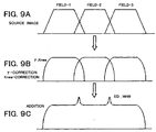
- the signal processing apparatus adds the plurality of video signals obtained by the high speed imaging to generates a standard speed video signals, but in this case, in the imaging apparatus, the video signals shown in FIG. 9A deform as shown in FIG. 9B due to the gamma processing and knee processing, so if combining these to generate a standard speed video signal, as shown in FIG. 9C , it suffers from the disadvantages that the standard speed video signal will suffer from unnatural edges or tones and the picture quality will become lower.
- EP 1014706 discloses a high-speed image pickup apparatus that obtains the same image quality as that of a standard-speed image pickup by simply converting a high-speed video signal into a plurality of standard-speed video signals.
- a video camera system comprises a video camera for outputting a video signal by picking up an object at a high speed.
- a transmitting path transmits the video signal to a signal processor.
- the signal processor signal-processes the transmitted video signal, and divides the high-speed video signal into a plurality of standard-speed video signals directly or by providing a blank field as an additional period by the video camera.
- the plurality of standard-speed video signals are transmitted by a transmitting path. By dividing a high-speed video signal into a plurality of channels of standard signals and signalprocessing them, a high-speed photographing video camera system can be formed simply.
- HDC-3300 HD Super Motion Color Camera discloses a device in the MAV-555 series that is MPEG based multi-channel editing disk recorder that combines advanced disk technology with a VTR-style of control proven in the day-to-day operation of broadcast operations.
- a video signal transfer system of a first aspect of the invention has an imaging apparatus for capturing an object to be imaged and generating a consecutive plurality of picture data forming a moving image, selecting from the plurality of picture data picture data positioned in advance at predetermined intervals to generate a plurality of lines (series) of video signals, and transmitting the plurality of lines of video signal, and a signal processing apparatus having a plurality of lines processing circuits, outputting the plurality of systems of video signals received from the imaging apparatus to the plurality of signal processing circuits, and making them process the signals in parallel.
- An imaging apparatus of a second aspect of the invention is an imaging apparatus transmitting imaging results to a signal processing apparatus having an imaging unit for capturing an object to be imaged and generating a consecutive plurality of picture data forming a moving image, a signal processing circuit for selecting from the plurality of picture data generated by the imaging unit the picture data positioned at predetermined intervals in advance to generate a plurality of lines (series) of video signals, and a transfer circuit for transmitting the plurality of lines of video signals generated by the signal processing circuit to the signal processing apparatus.
- a signal processing apparatus of a third aspect of the invention is a signal processing apparatus for processing a plurality of lines (series) of video signals received from an imaging apparatus capturing an object to be imaged to generate a consecutive plurality of picture data forming a moving image, selecting from the plurality of picture data the picture data positioned at predetermined intervals in advance to generate N ( ⁇ 2) lines (series) of video signals, having N number of signal processing circuits, a separating unit for outputting the N systems of video signals received from the imaging apparatus to the N number of signal processing circuits and making them process the signals in parallel, and an external apparatus outputting 1/N picture time's worth of picture data of the N number of video signals input from the N number of the signal processing circuits in one picture time.
- a video signal transfer method of a fourth aspect of the invention is a video signal transfer method transmitting imaging results of an imaging apparatus to a signal processing apparatus, having a first step of having the imaging apparatus configured to capture an object to be imaged and generate a consecutive plurality of picture data forming a moving image, a second step of having the imaging apparatus select from the plurality of picture data generated at the first step the picture data positioned at predetermined intervals in advance to generate a plurality of lines (series) of video signals and transmit the plurality of lines of video signals to the signal processing apparatus, and a third step of having the signal processing apparatus output the plurality of lines of video signals received from the imaging apparatus at the second step to the plurality of signal processing circuits and make them process the signals in parallel.
- a video signal transfer system enabling reduction of the amount of processing of the imaging apparatus when transferring a video signal generated by an imaging apparatus to a signal processing system.
- the present invention can provide a video signal transfer system, imaging apparatus, signal processing apparatus, and video signal transfer method able to suppress a drop in quality of the video signal output by the above signal processing apparatus.
- the video camera 10 is one example of an imaging apparatus of the present invention
- a camera control unit 12 is one example of a signal processing apparatus of the present invention.
- field pictures or frame pictures of the present embodiment are examples of the picture data of the present invention.
- video signals S34_1, S34_2, S34_3 of the present embodiment are examples of the plurality of lines (series) of video signals of the present invention.
- signal processing circuits 43_1, 43_2, 43_3 of the present embodiment are examples of the plurality of signal processing circuits of the present invention.
- the buffer memory 32 is an example of the memory of the present invention
- the viewfinder 33 is an example of the display of the present invention
- the signal processing circuit 34 is an example of the signal processing unit of the present invention.
- the preprocessing circuit 42 is an example of the separating unit of the present invention
- the addition circuit 71 is an example of the addition circuit of the present invention.
- FIG. 1 is a view of the overall configuration of a camera system 1 of the present embodiment.
- the camera system 1 has, for example, a video camera 10, camera control unit 12, and VTR or switcher (herein after VTR/switcher) 14.
- An external apparatus 20 is connected to the VTR/switcher 14.
- the video camera 10 generates a video signal in accordance with the imaging results and outputs it through an optical fiber cable 16 to the control unit 12.
- the camera control unit 12 processes the video signal inputted from the video camera 10 to generate an SDI (serial digital interface) type of video signal based on the SMPTE and outputs this through a cable 18 to the VTR/switcher 14.
- SDI serial digital interface
- the VTR/switcher 14 records or transmits the video signal inputted from the camera control unit 12.
- the optical fiber cable 16 for example, is a composite optical fiber cable made up of optical fiber for transmitting and receiving and metacables for power line and control use.
- the video camera 10 is arranged in a studio, and the camera control unit 12 and VTR/switcher 14 are arranged in a secondary adjustment room.
- this video signal and audio signal are outputted through the optical fiber cable 16 to the camera control unit 12 of the secondary adjustment room.
- the processed video signal and audio signal from the camera control unit 12 is outputted through the cable 18 to the VTR/switcher 14.
- VTR/switcher 14 performs signal processing for recording, editing, and transmitting the video signal and audio signal.
- FIG. 2 is a view of the configuration of the video camera 10 and the camera control unit 12.
- the video camera 10 as shown in FIG. 2 , has, for example, an imaging device 31, buffer memory 32, viewfinder 33, signal processing circuit 34, and transfer circuit 35.
- the imaging device 31 is, for example, a CMOS (Complementary Metal Oxide Semiconductor), CCD (Charge-Coupled Device), or other imaging device and outputs a video signal 31 in accordance with the imaging results to the signal processing circuit 34.
- CMOS Complementary Metal Oxide Semiconductor
- CCD Charge-Coupled Device
- the imaging device 31 for example, performs high speed imaging at 3X (three times worth) speed of the standard (normal) speed and generates an interlace format video signal S31.
- the imaging device 31 adjusted by a focusing mechanism. Further, the imaging results of the imaging device 31 are output as the video signal S31 after gain control.
- the buffer memory 32 stores the video signal processed in the signal processing circuit 34.
- the viewfinder 33 reads out and displays the video signal S31 stored in the buffer memory 32 under the control of the signal processing circuit 34.
- FIG. 3 is a view of the configuration of the signal processing circuit shown in FIG. 2 .
- the signal processing circuit 34 has, for example, an A/D conversion circuit 61, signal processing circuit 62, memory access circuit 63, and rearrangement circuit 64.
- the A/D conversion circuit 61 converts an analog video signal S31 inputted from the imaging device 31 to a digital video signal and outputs it to the signal processing circuit 62.
- the signal processing circuit 62 processes the digital video signal inputted from the A/D conversion circuit 61 relating to feedback control so as to generate the video signal S34a and outputs it to the memory access circuit 63.
- the memory access circuit 63 writes the video signal S34a in the buffer memory 32.
- the signal processing relating to the above feedback control includes gain control processing and auto alias level detection processing etc.
- the memory access circuit 63 writes the video signal S34a inputted from the signal processing circuit 62 in the buffer memory 32.
- the memory access circuit 63 reads out one of the fields for each consecutive 3 fields in the video signal S34a from the buffer memory 32 and outputs it to the viewfinder 33.
- the rearrangement circuit 64 receives as input the video signal S34a read by the memory access circuit 63 from the buffer memory 32.
- the video signal S31 is of an interlace format, it rearranges the video signal S34a, as shown in FIG. 4 , so that the former 3 fields 1T, 1B, 2T of 6 fields forming one group match in time (become parallel) and outputs them as the video signal S34 to the transfer circuit 35.
- T indicates a top field
- B indicates a bottom field
- the rearrangement circuit 64 rearranges, after the above former 3 fields 1T, 1B, 2T, the latter 3 fields 2B, 3T, and 3B of the above 6 fields so as to match in time (become parallel) and outputs them as the video signal S34 to the transfer circuit 35.
- the rearrangement circuit 64 as shown in FIG. 4B , generates a video signal comprised of three lines (series) of video signals S34_1, S34_2, S34_3.
- the latter camera control unit 12 can realize the processing for adding the 3X speed captured field pictures and displaying of a standard speed image by a simple addition circuit.
- the transfer circuit 35 transmits the video signal S34 inputted from the rearrangement circuit 64 in parallel or by time division through the optical fiber cable 16 to the camera control unit 12.
- the transfer circuit 35 transmits one 10.692GHz video signal S34 comprised of R, G, B 12-bit signals mapped to a serial signal to the optical fiber cable 16.
- the transfer circuit 35 may transmit the video signal S34 as six 1.485GHz serial SDI signals through a BNC cable to the control unit 12.
- the 3X speed (three times worth speed to a normal speed) is an example.
- the present embodiment may also be applied to high speed transfer (NX (N times worth) speed transmission) other than 3X speed.
- the video camera 10 transmits the video signal S34 of the format shown in FIG. 4 to the camera control unit 12 regardless of the speed of the video signal S12 outputted by the camera control unit.
- the video signal is processed relating to feedback control, but Knee processing or gamma correction processing or other predetermined processing for improvement of quality, compression, etc. are not performed.
- the processing load of the video camera 10 can be reduced more than before.
- the camera control unit 12 has, as shown in FIG. 2 , a transfer circuit 41, preprocessing circuit 42, signal processing circuit 43_1, 43_2, 43_3, 45, and format conversion circuit 47.
- the transfer circuit 41 performs reverse format conversion from the transfer circuit 35 on the video signal S34 received through the optical fiber cable 16 from the video camera 10 and outputs the result to the preprocessing circuit 42.
- FIG. 5 is a view of the configuration of the preprocessing circuit 42 as shown in FIG. 2 .
- the preprocessing circuit 42 outputs the video signals S34_1, S34_2, S34_3 forming the video signal S34 inputted from the transfer circuit 41 to the signal processing circuits 43_1, 43_2, 43_3.
- the preprocessing circuit 42 as shown in FIG. 5 , is provided with an addition circuit 71.
- the addition circuit 71 adds the video signals S34_1, S34_2, S34_3 forming the video signal S34 inputted from the transfer circuit 41 to generate the standard speed video signal S42 and outputs it to the signal processing circuit 45.
- the video signal S34 as shown in FIG. 4(B) , includes three lines (series) of video signals S34_1, S34_2, S34_3 stored in parallel, so there is no need to provide a memory for storing a large amounts of video signals before addition by the addition circuit 71.
- the signal processing circuits 43_1, 43_2, 43_3 process the video signals S34_1, S34_2, S34_3 for predetermined improvement of the quality, compression, etc. so as to generate the video signals S43_1, S43_2, S43 and outputs these as the video signal S12 to the VTR/switcher shown in FIG. 1 .
- the above signal processing performed by the signal processing circuits 43_1, 43_2, 43_3 include, for example, Knee processing (processing to compress multi-bits of pixel data to reduce load of color processing), gamma correction functions (processing to maximize input value to ideal output value in order to give vivid color), detail processing, etc.
- the signal processing circuits 43_1, 43_2, 43_3, for example, when reading out and replaying video signals stored in the VTR/switcher 14, perform processing to expand the read compressed video signals.
- the expanded video signals are outputted through the transfer circuit 41 to the video camera 10.
- the signal processing circuit 45 processes the standard speed video signal imputed from the preprocessing circuit 42 for predetermined improvement of quality, compression, etc. to generate the video signal S45 and outputs this as the video signal S12 to the VTR/switcher shown in FIG. 1 .
- the format conversion circuit 47 receives as input the video signal S45 from the signal processing circuit 45, converts it to a video signal 47 of a predetermined format, and outputs it as the video signal S12 to the VTR/switcher 14 shown in FIG. 1 .
- This conversion for example, is conversion that down converts an HD (High Definition) video signal to an SD (Standard Definition) video signal (NTSC system etc.).
- the VTR/switcher 14 in the case of 3X speed video output, as shown in FIG. 6(B) , switches the video signals S43_1, S43_2, S43_3 inputted from the signal processing circuits 43_1, 43_2, 43_3 and outputs the 3X speed video signal S14.
- the switch 48 in the case of standard speed video output, as shown in FIG. 6(C) , outputs the video signal S45, obtained by adding the video signals S43_1, S43_2, S43_3 inputted from the signal processing circuit, as the standard speed video signal S14.
- the camera control unit 12 can output the 3X speed or standard speed video signal S14 by just processing for switching the video signals S14 inputted from the camera control unit 12.
- the VTR/switcher 14 for example, also has the function of writing the video signal S12 inputted from the camera control unit 12 on to a disk or other recording unit and rearranging it for output when reading it.
- the imaging device of the video camera 10 generates a video signal S31 in accordance with the imaging results of the imaging subject.
- the A/D conversion circuit 61 of the signal processing circuit 34 shown in FIG. 3 converts the video signal S31 to a digital format and writes the processed video signal S31a through the memory access circuit 63 in the buffer memory 32.
- the rearrangement circuit 64 receives as input the video signal S34a read from the buffer memory 32 through the memory access circuit 63.
- the video signal S31 is of an interlace format
- it rearranges the video signal S34a, as shown in FIG. 4 , so that the former 3 field pictures 1T, 1B, 2T of the 6 fields forming a group match in time (become parallel) and outputs them as the video signal S34 comprised of the three lines of standard speed video signals S34_1, S34_2, S34_3.
- the transfer circuit 35 transmits the video signal S34 inputted from the rearrangement circuit 64 in parallel or by time division through the optical fiber cable 16 to the camera control unit 12.
- the transfer circuit 41 of the camera control unit 12 performs reverse format conversion from the transfer circuit 35 on the video signal S34 received through the optical fiber cable 16 from the video camera 10 and outputs the result to the preprocessing circuit 42.
- the preprocessing circuit 42 of the camera control unit 12 outputs the video signals S34_1, S34_2, S34_3 forming the video signal S34 inputted from the transfer circuit 41 to the signal processing circuits 43_1, 43_2, 43_3.
- the addition circuit 71 adds the video signals S34_1, S34_2, S34_3 forming the video signal S34 inputted from the transfer circuit to generate the standard speed video signal S42 and outputs it to the signal processing circuit 45.
- the signal processing circuits 43_1, 43_2, 43_3 process the video signals S34_1, S34_2, S34_3 for predetermined improvement of quality, compression, etc. to generate the video signals S43_1, S43_2, S43_3 and outputs them as the video signal S12 to the VTR/switcher 14.
- the signal processing circuit 45 has processes the standard speed video signal inputted from the preprocessing circuit 42 for predetermined improvement of quality, compression, etc. to generate the video signal S45 and outputs it as the video signal S12 to the VTR/switcher 14.
- the VTR/switcher 14 in the case of 3X speed video output, as shown in FIG. 6B , switches from the video signals S43_1, S43_2, S43_3 inputted from the signal processing circuits 43_1, 43_2, 43_3 and outputs the 3X speed video signal S_14.
- the VTR/switcher 14 in the case of standard speed video output, as shown in FIG. 6C , outputs the video signal S45, obtained by adding the video signals S43_1, S43_2, S43_3 inputted from the signal processing circuit, as the standard speed video signal S14.
- the rearrangement circuit 64 of the video camera 10 shown in FIG. 3 generates three systems of 1X speed video signals S34_1, S34_2, S34_3 from the video signal S31 captured at 3X speed shown in FIG. 4A and transmits it to the camera control unit 12 in accordance with their timings.
- the camera control unit 12 performs parallel processing on the video signals S34_1, S34_2, S34_3 received from the video camera 10 at the signal processing circuits 43_1, 43_2, 43_3 shown in FIG. 2 .
- the camera control unit 12 can process a video signal captured at 3X speed in a short time.
- the signal processing circuit 62 of the video camera 10 shown in FIG. 3 processes the digital video signal inputted from the A/D conversion circuit 61 for gain control, auto alias level detection, or other feedback control.
- the signal processing circuits 43_1, 43_2, 43_3 of the camera control unit 12 process the video signals S34_1, S34_2, S34_3 for Knee processing, gamma correction, or other predetermined improvement of quality, compression, etc.
- the addition circuit 71 of the preprocessing circuit 42 shown in FIG. 5 adds the three systems of video signals to generate a standard speed video signal, as shown in FIGS. 7B and 7C , it can add them in a state without image processing and can therefore avoid a drop in quality as explained with reference to FIG. 9 .
- the image processing for improvement of quality is not performed by the video camera 10, but by the camera control unit 12, so the amount of processing and power consumption of the video camera 10 can be reduced.
- This effect is particularly remarkable in the case of using, as a video signal, an HD signal with several times larger an amount of data than SD.
- the video camera 10 temporarily stores the picture data generated at the imaging device 31 in the buffer memory 32, then reads it out and displays the image on the viewfinder 33. For this reason, even when no communication link is established between the video camera 10 and the camera control unit 12, it is still possible to display a captured image on the viewfinder 33. Due to this, the system setup can be made more efficient.
- the viewfinder 33 can display an image with almost no delay and can track and display an image of an object moving at a high speed.
- the video camera 10 In the camera system 1, the video camera 10 generates three lines of standard speed video signals S34_1, S34_2, S34_3 from the high speed captured video signal S31 and transmits them to the camera control unit 12. Further, the camera control unit 12 processes the three lines of standard speed video signals S34_1, S34_2, S34_3 at the signal processing circuits 43_1, 43_2, 43_3 in parallel, then switches and outputs the results so as to output a 3X speed video signal.
- the video signals S34_1, S34_2, S34_3 can be constantly processed at standard speed, and the circuit configuration can be made simple and inexpensive.
- the video camera 10 generates three lines of standard speed video signals S34_1, S34_2, S34_3, so the camera control unit 12 does not need to be provided with a large scale memory.
- the effect is particularly remarkable in cases where, as the video signal, an HD image with several times the amount of data compared with the SD is used.
- common signal processing circuits can be used as the signal processing circuits 43_1, 43_2, 43_3, so even if the image capture speed is increased to 3X (three times) or more, this can be handled by just increasing the same signal processing circuits.
- the video signal transmitted from the video camera 10 to the camera control unit 12 is not compressed, so high quality video output is possible.
- a standard speed video signal is generated by addition before camera signal processing by the signal processing circuit 45, so it is possible to output high quality video as standard speed video.
- the standard speed video is high quality, usage as a standard speed imaging camera and not just as a high speed imaging camera is possible.
- high speed video and standard speed video can be outputted at the same time, so it is possible to combine the two separate lines required for high speed imaging and standard speed imaging into one.
- the types of signals that can be taken by the camera are increased and flexible application as a system is possible.
- the processed signal to be displayed on the viewfinder 33 may be selected from one with an added natural dynamic resolution feel or a high speed video with a shutter effect, so the optimal video (picture) can be displayed on the viewfinder 33 in accordance with the objective.
- the video signal returning from the camera control unit 12 to the video camera 10 for display on the viewfinder 33 may be selected from one system of processed high speed output with a shutter effect or added standard speed video with natural motion.
- the imaging device 31 generated a video signal 31a of an interlaced format, however, in the present embodiment, as shown in FIG. 8A , the imaging device 31a generates a video signal S31a of a progressive format.
- the rearrangement circuit 64 assigns consecutive frames (for example, “1”, “2”, “3") in groups of three frames to the plurality of different video signals S34_1a, S34_2a, S34_3a.
- the present invention is not limited to the above embodiments.
Landscapes
- Engineering & Computer Science (AREA)
- Multimedia (AREA)
- Signal Processing (AREA)
- Computing Systems (AREA)
- Theoretical Computer Science (AREA)
- Studio Devices (AREA)
- Color Television Image Signal Generators (AREA)
Description
- The present invention contains subject matter related to Japanese Patent Application No.
2005-261066 2005-330533 - The present invention relates to a video signal transfer system for transmitting video signals captured by a video camera for example to a later signal processing system and to an imaging apparatus, a signal processing apparatus, and a video signal transfer method used for that.
- For example, there is a video signal transfer system which performs high speed imaging at a high resolution by an imaging apparatus and transmits that video signal from the imaging apparatus to a signal processing apparatus.
- Such a video signal transfer system performs control, in accordance with what speed the signal processing apparatus outputs the video signal, to transmit a video signal of that speed from the imaging apparatus to the signal processing apparatus.
- Further, the imaging apparatus processes the video signal for gain control and auto alias level detection or other feedback processing, knee processing, and gamma correction. (refer to Japanese Patent Publication (A) No.
2000-188703 - Further, the signal processing apparatus serially processes the video signal captured at a high speed imaging for color correction etc.
- However, in the above-mentioned video signal transfer system, since the speed of the video signal transmitted from the imaging apparatus to the signal processing apparatus is controlled in accordance with the speed of the video signal outputted by the signal processing apparatus, it suffers from the disadvantages that the amount of processing of the imaging apparatus is large, reduction of size is difficult, and the small size is complicated, and the power consumption is large.
- Further, the signal processing apparatus adds the plurality of video signals obtained by the high speed imaging to generates a standard speed video signals, but in this case, in the imaging apparatus, the video signals shown in
FIG. 9A deform as shown inFIG. 9B due to the gamma processing and knee processing, so if combining these to generate a standard speed video signal, as shown inFIG. 9C , it suffers from the disadvantages that the standard speed video signal will suffer from unnatural edges or tones and the picture quality will become lower. -
EP 1014706 discloses a high-speed image pickup apparatus that obtains the same image quality as that of a standard-speed image pickup by simply converting a high-speed video signal into a plurality of standard-speed video signals. A video camera system comprises a video camera for outputting a video signal by picking up an object at a high speed. A transmitting path transmits the video signal to a signal processor. The signal processor signal-processes the transmitted video signal, and divides the high-speed video signal into a plurality of standard-speed video signals directly or by providing a blank field as an additional period by the video camera. The plurality of standard-speed video signals are transmitted by a transmitting path. By dividing a high-speed video signal into a plurality of channels of standard signals and signalprocessing them, a high-speed photographing video camera system can be formed simply. - "HDC-3300 HD Super Motion Color Camera" discloses a device in the MAV-555 series that is MPEG based multi-channel editing disk recorder that combines advanced disk technology with a VTR-style of control proven in the day-to-day operation of broadcast operations.
- It is therefore desirable in the present invention to provide a video signal transfer system, imaging apparatus, signal processing apparatus, and video signal transfer method enabling reduction of the amount of processing of the imaging apparatus when transferring a video signal generated by the imaging apparatus to the signal processing apparatus.
- It is also desirable in, the present invention to provide a video signal transfer system, imaging apparatus, signal processing apparatus, and video signal transfer method able to suppress a drop in quality of the video signal output by the above signal processing apparatus.
- A video signal transfer system of a first aspect of the invention has an imaging apparatus for capturing an object to be imaged and generating a consecutive plurality of picture data forming a moving image, selecting from the plurality of picture data picture data positioned in advance at predetermined intervals to generate a plurality of lines (series) of video signals, and transmitting the plurality of lines of video signal, and a signal processing apparatus having a plurality of lines processing circuits, outputting the plurality of systems of video signals received from the imaging apparatus to the plurality of signal processing circuits, and making them process the signals in parallel.
- An imaging apparatus of a second aspect of the invention is an imaging apparatus transmitting imaging results to a signal processing apparatus having an imaging unit for capturing an object to be imaged and generating a consecutive plurality of picture data forming a moving image, a signal processing circuit for selecting from the plurality of picture data generated by the imaging unit the picture data positioned at predetermined intervals in advance to generate a plurality of lines (series) of video signals, and a transfer circuit for transmitting the plurality of lines of video signals generated by the signal processing circuit to the signal processing apparatus.
- A signal processing apparatus of a third aspect of the invention is a signal processing apparatus for processing a plurality of lines (series) of video signals received from an imaging apparatus capturing an object to be imaged to generate a consecutive plurality of picture data forming a moving image, selecting from the plurality of picture data the picture data positioned at predetermined intervals in advance to generate N (≥2) lines (series) of video signals, having N number of signal processing circuits, a separating unit for outputting the N systems of video signals received from the imaging apparatus to the N number of signal processing circuits and making them process the signals in parallel, and an external apparatus outputting 1/N picture time's worth of picture data of the N number of video signals input from the N number of the signal processing circuits in one picture time.
- A video signal transfer method of a fourth aspect of the invention is a video signal transfer method transmitting imaging results of an imaging apparatus to a signal processing apparatus, having a first step of having the imaging apparatus configured to capture an object to be imaged and generate a consecutive plurality of picture data forming a moving image, a second step of having the imaging apparatus select from the plurality of picture data generated at the first step the picture data positioned at predetermined intervals in advance to generate a plurality of lines (series) of video signals and transmit the plurality of lines of video signals to the signal processing apparatus, and a third step of having the signal processing apparatus output the plurality of lines of video signals received from the imaging apparatus at the second step to the plurality of signal processing circuits and make them process the signals in parallel.
- According to the present invention, it is achieved a video signal transfer system, imaging apparatus, signal processing apparatus, and video signal transfer method enabling reduction of the amount of processing of the imaging apparatus when transferring a video signal generated by an imaging apparatus to a signal processing system.
- Further, the present invention can provide a video signal transfer system, imaging apparatus, signal processing apparatus, and video signal transfer method able to suppress a drop in quality of the video signal output by the above signal processing apparatus.
- These and other objects and features of the present invention will become clearer from the following description of the preferred embodiments given with reference to the attached drawings, wherein:
-
FIG. 1 is a view of the configuration of a video signal capturing, video signal processing, and transferring system of a first embodiment of the present invention; -
FIG. 2 is a view of the configuration of a video camera and a video signal processing and control unit shown inFIG. 1 ; -
FIG. 3 is a diagram showing the configuration of an image signal processor circuit in the video camera shown inFIG. 2 ; -
FIGS. 4A to 4B are diagrams showing the image signal transferred by the image signal processor circuit shown inFIG. 3 ; -
FIG. 5 is a diagram showing the configuration of a normal speed image signal generator circuit shown inFIG. 2 ; -
FIGS. 6A to 6C are diagrams for explaining a switching operation of the video signal processing and control unit shown inFIG. 2 ; -
FIGS. 7A to 7D are diagrams showing processing results of the image signal according to a first embodiment of the present invention; -
FIGS. 8A to 8B are diagrams for explaining the image signal according to a second embodiment of the present invention; and -
FIGS. 9A to 9C are diagrams for explaining the problem in a conventional signal transferring system. - Below, the camera system according to embodiments of the present invention will be explained.
- First, the correspondence between the components of the present embodiment and the components of the present invention will be explained.
- The
video camera 10 is one example of an imaging apparatus of the present invention, and acamera control unit 12 is one example of a signal processing apparatus of the present invention. - Further, the field pictures or frame pictures of the present embodiment are examples of the picture data of the present invention.
- Further, the video signals S34_1, S34_2, S34_3 of the present embodiment are examples of the plurality of lines (series) of video signals of the present invention.
- Further, the signal processing circuits 43_1, 43_2, 43_3 of the present embodiment are examples of the plurality of signal processing circuits of the present invention.
- Further, the
buffer memory 32 is an example of the memory of the present invention, theviewfinder 33 is an example of the display of the present invention, and thesignal processing circuit 34 is an example of the signal processing unit of the present invention. - Further, the
preprocessing circuit 42 is an example of the separating unit of the present invention, and theaddition circuit 71 is an example of the addition circuit of the present invention. -
FIG. 1 is a view of the overall configuration of acamera system 1 of the present embodiment. - As shown in
FIG. 1 , thecamera system 1 has, for example, avideo camera 10,camera control unit 12, and VTR or switcher (herein after VTR/switcher) 14. Anexternal apparatus 20 is connected to the VTR/switcher 14. - The
video camera 10 generates a video signal in accordance with the imaging results and outputs it through anoptical fiber cable 16 to thecontrol unit 12. - The
camera control unit 12 processes the video signal inputted from thevideo camera 10 to generate an SDI (serial digital interface) type of video signal based on the SMPTE and outputs this through acable 18 to the VTR/switcher 14. - The VTR/
switcher 14 records or transmits the video signal inputted from thecamera control unit 12. - The
optical fiber cable 16, for example, is a composite optical fiber cable made up of optical fiber for transmitting and receiving and metacables for power line and control use. - In the
camera system 1, for example, thevideo camera 10 is arranged in a studio, and thecamera control unit 12 and VTR/switcher 14 are arranged in a secondary adjustment room. - Due to this, when recording a program by the
video camera 10 in the studio, this video signal and audio signal are outputted through theoptical fiber cable 16 to thecamera control unit 12 of the secondary adjustment room. - Further, the processed video signal and audio signal from the
camera control unit 12 is outputted through thecable 18 to the VTR/switcher 14. - Further, the VTR/
switcher 14 performs signal processing for recording, editing, and transmitting the video signal and audio signal. - Below, the
video camera 10 andcamera control unit 12 will be explained in detail. -
FIG. 2 is a view of the configuration of thevideo camera 10 and thecamera control unit 12. - The
video camera 10, as shown inFIG. 2 , has, for example, animaging device 31,buffer memory 32,viewfinder 33,signal processing circuit 34, andtransfer circuit 35. - The
imaging device 31 is, for example, a CMOS (Complementary Metal Oxide Semiconductor), CCD (Charge-Coupled Device), or other imaging device and outputs avideo signal 31 in accordance with the imaging results to thesignal processing circuit 34. - The
imaging device 31, for example, performs high speed imaging at 3X (three times worth) speed of the standard (normal) speed and generates an interlace format video signal S31. - Note that light is focused on the
imaging device 31 adjusted by a focusing mechanism. Further, the imaging results of theimaging device 31 are output as the video signal S31 after gain control. - The
buffer memory 32 stores the video signal processed in thesignal processing circuit 34. - The
viewfinder 33 reads out and displays the video signal S31 stored in thebuffer memory 32 under the control of thesignal processing circuit 34. -
FIG. 3 is a view of the configuration of the signal processing circuit shown inFIG. 2 . - As shown in
FIG. 3 , thesignal processing circuit 34 has, for example, an A/D conversion circuit 61,signal processing circuit 62,memory access circuit 63, andrearrangement circuit 64. - The A/
D conversion circuit 61 converts an analog video signal S31 inputted from theimaging device 31 to a digital video signal and outputs it to thesignal processing circuit 62. - The
signal processing circuit 62 processes the digital video signal inputted from the A/D conversion circuit 61 relating to feedback control so as to generate the video signal S34a and outputs it to thememory access circuit 63. Thememory access circuit 63 writes the video signal S34a in thebuffer memory 32. - In the present embodiment, the signal processing relating to the above feedback control, for example, includes gain control processing and auto alias level detection processing etc.
- The
memory access circuit 63 writes the video signal S34a inputted from thesignal processing circuit 62 in thebuffer memory 32. - Further, the
memory access circuit 63 reads out one of the fields for each consecutive 3 fields in the video signal S34a from thebuffer memory 32 and outputs it to theviewfinder 33. - The
rearrangement circuit 64 receives as input the video signal S34a read by thememory access circuit 63 from thebuffer memory 32. When the video signal S31 is of an interlace format, it rearranges the video signal S34a, as shown inFIG. 4 , so that the former 3fields transfer circuit 35. - In
FIG. 4 , "T" indicates a top field, and "B" indicates a bottom field. - Further, the
rearrangement circuit 64, as shown inFIG. 4 , rearranges, after the above former 3fields fields transfer circuit 35. - That is, the
rearrangement circuit 64, as shown inFIG. 4B , generates a video signal comprised of three lines (series) of video signals S34_1, S34_2, S34_3. - In the
camera system 1, by thesignal processing circuit 34 of thevideo camera 10 rearranging field pictures in groups of 6 field pictures as explained usingFIG. 4 , the lattercamera control unit 12 can realize the processing for adding the 3X speed captured field pictures and displaying of a standard speed image by a simple addition circuit. - The
transfer circuit 35 transmits the video signal S34 inputted from therearrangement circuit 64 in parallel or by time division through theoptical fiber cable 16 to thecamera control unit 12. - For example, the
transfer circuit 35 transmits one 10.692GHz video signal S34 comprised of R, G, B 12-bit signals mapped to a serial signal to theoptical fiber cable 16. - Further, in the case of 3X (three times worth) speed transmission, the
transfer circuit 35 may transmit the video signal S34 as six 1.485GHz serial SDI signals through a BNC cable to thecontrol unit 12. Note that the 3X speed (three times worth speed to a normal speed) is an example. The present embodiment may also be applied to high speed transfer (NX (N times worth) speed transmission) other than 3X speed. - As explained above, the
video camera 10 transmits the video signal S34 of the format shown inFIG. 4 to thecamera control unit 12 regardless of the speed of the video signal S12 outputted by the camera control unit. - Further, in
camera system 1, as explained above, the video signal is processed relating to feedback control, but Knee processing or gamma correction processing or other predetermined processing for improvement of quality, compression, etc. are not performed. - Due to this, the processing load of the
video camera 10 can be reduced more than before. - The
camera control unit 12 has, as shown inFIG. 2 , atransfer circuit 41, preprocessingcircuit 42, signal processing circuit 43_1, 43_2, 43_3, 45, andformat conversion circuit 47. - The
transfer circuit 41 performs reverse format conversion from thetransfer circuit 35 on the video signal S34 received through theoptical fiber cable 16 from thevideo camera 10 and outputs the result to thepreprocessing circuit 42. -
FIG. 5 is a view of the configuration of thepreprocessing circuit 42 as shown inFIG. 2 . - The
preprocessing circuit 42, as shown inFIG. 5 , outputs the video signals S34_1, S34_2, S34_3 forming the video signal S34 inputted from thetransfer circuit 41 to the signal processing circuits 43_1, 43_2, 43_3. - Further, the
preprocessing circuit 42, as shown inFIG. 5 , is provided with anaddition circuit 71. - The
addition circuit 71 adds the video signals S34_1, S34_2, S34_3 forming the video signal S34 inputted from thetransfer circuit 41 to generate the standard speed video signal S42 and outputs it to thesignal processing circuit 45. - In the present embodiment, the video signal S34, as shown in
FIG. 4(B) , includes three lines (series) of video signals S34_1, S34_2, S34_3 stored in parallel, so there is no need to provide a memory for storing a large amounts of video signals before addition by theaddition circuit 71. - The signal processing circuits 43_1, 43_2, 43_3 process the video signals S34_1, S34_2, S34_3 for predetermined improvement of the quality, compression, etc. so as to generate the video signals S43_1, S43_2, S43 and outputs these as the video signal S12 to the VTR/switcher shown in
FIG. 1 . - The above signal processing performed by the signal processing circuits 43_1, 43_2, 43_3 include, for example, Knee processing (processing to compress multi-bits of pixel data to reduce load of color processing), gamma correction functions (processing to maximize input value to ideal output value in order to give vivid color), detail processing, etc.
- Further, the signal processing circuits 43_1, 43_2, 43_3, for example, when reading out and replaying video signals stored in the VTR/
switcher 14, perform processing to expand the read compressed video signals. The expanded video signals are outputted through thetransfer circuit 41 to thevideo camera 10. - The
signal processing circuit 45 processes the standard speed video signal imputed from thepreprocessing circuit 42 for predetermined improvement of quality, compression, etc. to generate the video signal S45 and outputs this as the video signal S12 to the VTR/switcher shown inFIG. 1 . - The
format conversion circuit 47 receives as input the video signal S45 from thesignal processing circuit 45, converts it to avideo signal 47 of a predetermined format, and outputs it as the video signal S12 to the VTR/switcher 14 shown inFIG. 1 . This conversion, for example, is conversion that down converts an HD (High Definition) video signal to an SD (Standard Definition) video signal (NTSC system etc.). - The VTR/
switcher 14, in the case of 3X speed video output, as shown inFIG. 6(B) , switches the video signals S43_1, S43_2, S43_3 inputted from the signal processing circuits 43_1, 43_2, 43_3 and outputs the 3X speed video signal S14. - On the other hand, the switch 48, in the case of standard speed video output, as shown in
FIG. 6(C) , outputs the video signal S45, obtained by adding the video signals S43_1, S43_2, S43_3 inputted from the signal processing circuit, as the standard speed video signal S14. - In this way, the
camera control unit 12 can output the 3X speed or standard speed video signal S14 by just processing for switching the video signals S14 inputted from thecamera control unit 12. - Further, the VTR/
switcher 14, for example, also has the function of writing the video signal S12 inputted from thecamera control unit 12 on to a disk or other recording unit and rearranging it for output when reading it. - Below, an example of the operation of the
camera system 1 of the present embodiment will be explained. - First, the imaging device of the
video camera 10 generates a video signal S31 in accordance with the imaging results of the imaging subject. - Next, the A/
D conversion circuit 61 of thesignal processing circuit 34 shown inFIG. 3 converts the video signal S31 to a digital format and writes the processed video signal S31a through thememory access circuit 63 in thebuffer memory 32. - Next, the
rearrangement circuit 64 receives as input the video signal S34a read from thebuffer memory 32 through thememory access circuit 63. When the video signal S31 is of an interlace format, it rearranges the video signal S34a, as shown inFIG. 4 , so that the former 3field pictures - The
transfer circuit 35 transmits the video signal S34 inputted from therearrangement circuit 64 in parallel or by time division through theoptical fiber cable 16 to thecamera control unit 12. - The
transfer circuit 41 of thecamera control unit 12 performs reverse format conversion from thetransfer circuit 35 on the video signal S34 received through theoptical fiber cable 16 from thevideo camera 10 and outputs the result to thepreprocessing circuit 42. - Next, the
preprocessing circuit 42 of thecamera control unit 12, as shown inFIG. 5 , outputs the video signals S34_1, S34_2, S34_3 forming the video signal S34 inputted from thetransfer circuit 41 to the signal processing circuits 43_1, 43_2, 43_3. - Further, the
addition circuit 71 adds the video signals S34_1, S34_2, S34_3 forming the video signal S34 inputted from the transfer circuit to generate the standard speed video signal S42 and outputs it to thesignal processing circuit 45. - Further, the signal processing circuits 43_1, 43_2, 43_3 process the video signals S34_1, S34_2, S34_3 for predetermined improvement of quality, compression, etc. to generate the video signals S43_1, S43_2, S43_3 and outputs them as the video signal S12 to the VTR/
switcher 14. - In parallel with this, the
signal processing circuit 45 has processes the standard speed video signal inputted from thepreprocessing circuit 42 for predetermined improvement of quality, compression, etc. to generate the video signal S45 and outputs it as the video signal S12 to the VTR/switcher 14. - Next, the VTR/
switcher 14, in the case of 3X speed video output, as shown inFIG. 6B , switches from the video signals S43_1, S43_2, S43_3 inputted from the signal processing circuits 43_1, 43_2, 43_3 and outputs the 3X speed video signal S_14. - On the other hand, the VTR/
switcher 14, in the case of standard speed video output, as shown inFIG. 6C , outputs the video signal S45, obtained by adding the video signals S43_1, S43_2, S43_3 inputted from the signal processing circuit, as the standard speed video signal S14. - As explained above, in the
camera system 1, as shown inFIG. 4 , therearrangement circuit 64 of thevideo camera 10 shown inFIG. 3 generates three systems of 1X speed video signals S34_1, S34_2, S34_3 from the video signal S31 captured at 3X speed shown inFIG. 4A and transmits it to thecamera control unit 12 in accordance with their timings. - Further, the
camera control unit 12 performs parallel processing on the video signals S34_1, S34_2, S34_3 received from thevideo camera 10 at the signal processing circuits 43_1, 43_2, 43_3 shown inFIG. 2 . - Due to this, the
camera control unit 12 can process a video signal captured at 3X speed in a short time. - Further, in the
camera system 1, thesignal processing circuit 62 of thevideo camera 10 shown inFIG. 3 processes the digital video signal inputted from the A/D conversion circuit 61 for gain control, auto alias level detection, or other feedback control. - Further, the signal processing circuits 43_1, 43_2, 43_3 of the
camera control unit 12 process the video signals S34_1, S34_2, S34_3 for Knee processing, gamma correction, or other predetermined improvement of quality, compression, etc. - Due to this, for example, when the
addition circuit 71 of thepreprocessing circuit 42 shown inFIG. 5 adds the three systems of video signals to generate a standard speed video signal, as shown inFIGS. 7B and 7C , it can add them in a state without image processing and can therefore avoid a drop in quality as explained with reference toFIG. 9 . - Further, in the
camera system 1, the image processing for improvement of quality is not performed by thevideo camera 10, but by thecamera control unit 12, so the amount of processing and power consumption of thevideo camera 10 can be reduced. This effect is particularly remarkable in the case of using, as a video signal, an HD signal with several times larger an amount of data than SD. - In the
camera system 1, thevideo camera 10 temporarily stores the picture data generated at theimaging device 31 in thebuffer memory 32, then reads it out and displays the image on theviewfinder 33. For this reason, even when no communication link is established between thevideo camera 10 and thecamera control unit 12, it is still possible to display a captured image on theviewfinder 33. Due to this, the system setup can be made more efficient. - Further, the
viewfinder 33 can display an image with almost no delay and can track and display an image of an object moving at a high speed. - In the
camera system 1, it is possible to change the speed of the video signal S14 in the VTR/switcher 14 without changing the capture speed of theimaging device 31. Due to this, operation control of theimaging device 31 becomes simple. - In the
camera system 1, thevideo camera 10 generates three lines of standard speed video signals S34_1, S34_2, S34_3 from the high speed captured video signal S31 and transmits them to thecamera control unit 12. Further, thecamera control unit 12 processes the three lines of standard speed video signals S34_1, S34_2, S34_3 at the signal processing circuits 43_1, 43_2, 43_3 in parallel, then switches and outputs the results so as to output a 3X speed video signal. - Due to this, the video signals S34_1, S34_2, S34_3 can be constantly processed at standard speed, and the circuit configuration can be made simple and inexpensive.
- Further, in the
camera system 1, thevideo camera 10 generates three lines of standard speed video signals S34_1, S34_2, S34_3, so thecamera control unit 12 does not need to be provided with a large scale memory. The effect is particularly remarkable in cases where, as the video signal, an HD image with several times the amount of data compared with the SD is used. Further, in thecamera system 1, common signal processing circuits can be used as the signal processing circuits 43_1, 43_2, 43_3, so even if the image capture speed is increased to 3X (three times) or more, this can be handled by just increasing the same signal processing circuits. - Further, in the
camera system 1, the video signal transmitted from thevideo camera 10 to thecamera control unit 12 is not compressed, so high quality video output is possible. - Further, in the
camera system 1, a standard speed video signal is generated by addition before camera signal processing by thesignal processing circuit 45, so it is possible to output high quality video as standard speed video. In this way, because the standard speed video is high quality, usage as a standard speed imaging camera and not just as a high speed imaging camera is possible. - In the past, high speed video and standard speed video can be outputted at the same time, so it is possible to combine the two separate lines required for high speed imaging and standard speed imaging into one.
- Further, in the
camera system 1, because there are a plurality of return systems (paths), the types of signals that can be taken by the camera are increased and flexible application as a system is possible. - Further, the processed signal to be displayed on the
viewfinder 33 may be selected from one with an added natural dynamic resolution feel or a high speed video with a shutter effect, so the optimal video (picture) can be displayed on theviewfinder 33 in accordance with the objective. - Further, the video signal returning from the
camera control unit 12 to thevideo camera 10 for display on theviewfinder 33 may be selected from one system of processed high speed output with a shutter effect or added standard speed video with natural motion. - In addition to this, as an independent return system is located in the
video camera 10, it is possible to obtain a video signal, other than the video signal displayed on theviewfinder 33, from the output terminal provided at the camera at the same time as displaying the video of the camera video returned from thecamera control unit 12. - In the above-mentioned first embodiment, a case was illustrated where the
imaging device 31 generated a video signal 31a of an interlaced format, however, in the present embodiment, as shown inFIG. 8A , the imaging device 31a generates a video signal S31a of a progressive format. - In this case, the
rearrangement circuit 64, as shown inFIG. 8B , assigns consecutive frames (for example, "1", "2", "3") in groups of three frames to the plurality of different video signals S34_1a, S34_2a, S34_3a. - In this way, when the
imaging device 31 generates a video signal S31a of a progressive format, effects similar to the case of the first embodiment can be obtained. - The present invention is not limited to the above embodiments.
- Namely, those skilled in the art can perform a variety of modifications, combinations, sub-combinations, and substitutions concerning the components of the embodiments mentioned above within the technical range of the claims.
- For example, in the above embodiments, a case was illustrated where "N" is "3" for the present invention, however, it is possible to apply the present invention in a situation of 2 or more.
- Further, in the above embodiments, a case was illustrated where only feedback processing was performed in the
video camera 10, however, even in cases where gamma correction and Knee processing etc., are performed in thevideo camera 10, since the processing of the video camera does not need to be altered in accordance with the speed of the video signal outputted from thecamera control unit 12, the effect of enabling thevideo camera 10 to be realized by a simple configuration can be obtained.
Claims (12)
- A video signal transfer system, comprising:an imaging apparatus (10) for capturing an object (OB) to be imaged and generating a consecutive plurality of picture data forming a moving image, for selecting from the plurality of picture data picture data position at predetermined time intervals to generate N(N≥2) video signals, wherein the imaging apparatus comprises a transfer circuit for transmitting the plurality of video signals through an optical fibre cable (16) to a camera control unit (12), andthe camera control unit (12) having N signal processing circuits (43-1, 43-2, ..., 45), the camera control unit (12) having a transfer circuit (41) configured to receive the plurality of video signals from the imaging apparatus (10) and configured to make the plurality of signal processing circuits process the video signals in parallel,wherein the camera control unit (12) comprises a separating unit (42) configured to output each of the plurality of video signals received from the imaging apparatus (10) to one of the signal processing circuits each, the signal processing circuits configured to process the plurality of video signals received from the imaging apparatus for predetermined improvement of quality,
characterised in thatthe separating unit (42) further comprises an adding unit (71) configured to receive in parallel and add the plurality of video signals separated by the separating unit (42) so as to generate a new standard speed video signal, andthat the camera control unit (12) comprises a further signal processing circuit (45) for knee processing, andthat the adding unit (71) is configured to output the new standard speed video signal to the further signal processing circuit (45), which is configured to process the new standard speed video signal for predetermined improvement of quality and to output the processed new standard speed video signal (S45). - The video signal transfer system as set forth in claim 1,
wherein the imaging apparatus (10) is configured to perform feedback processing, including gain control processing and/or auto alias level detection processing, the imaging apparatus (10) being configured to generate the moving image based on the picture data, and
the plurality of signal processing circuits (43-1, 43-2, ..., 45) of the camera control unit (12) is configured to process the plurality of video signals (43-1, 43-2, ..., 45) to compress or expand data. - The video signal transfer system as set forth in claim 1, wherein the imaging apparatus (10) comprises:an imaging unit (31) configured to generate the plurality of picture data,a processing unit (34) configured to process the plurality of picture data and adjust the imaging unit based on the plurality of picture data generated by the imaging unit, anda rearrangement unit (64) configured to generate the plurality of video signals.
- The video signal transfer system as set forth in claim 1,
wherein the plurality of video signals generated by the imaging apparatus (10) is N, N≥2,
wherein the imaging apparatus (10) is configured to store a N number of consecutive picture data forming the moving image, to control the N number of consecutive picture data so as to transmit them at the same time, and to transmit the plurality of video signals at 1/N speed of the moving image capture speed. - The video signal transfer system as set forth in claim 1, wherein the imaging apparatus (10) comprises
a memory (32) for storing the generated consecutive plurality of picture data,
a display (34) for displaying an image formed in accordance with the consecutive plurality of picture data stored in the memory, and
a rearrangement unit (64) configured to select from the consecutive plurality of picture data forming the moving image read out from the memory the picture data positioned at predetermined time intervals so as to generate a plurality of video signals and to generate the plurality of video signals. - The video signal transfer system as set forth in claim 1,
wherein the imaging apparatus (10) is configured to generate N (N ≥2) video signals, to store a N number of consecutive picture data forming the moving image, to control the N number of consecutive picture data so as to transmit them at substantially the same timing, and to transmit the plurality of video signals at 1/N speed of the image capture speed by the imaging apparatus (10), and
wherein the camera control unit (12) is configured to output the processed video signals from the N number of the signal processing circuits to an external apparatus (20) and
the external apparatus (20) is configured to output 1/N picture time's worth of picture data of one of the inputted N number of video signals in one picture time. - The video signal transfer system as set forth in claim 6,
wherein the external apparatus (20) is configured to select and to output one of the outputs of the N number of signal processing circuits (43-1, ...,43-3, 45) at 1/N speed of the image capture speed by the imaging apparatus (10). - The video transfer system as set forth in claim 1,
wherein the imaging apparatus (10) comprises a signal processing unit (34) configured to generate N (N ≥2) video signals, to store N (N ≥2) number of consecutive picture data forming the moving image in a different line of the video signal each, to control the N number of consecutive picture data to transmit them at substantially the same timing, and to transmit the plurality of video signals at 1/N speed of the image capture speed. - The video transfer system as set forth in claim 8, wherein the signal processing unit (34) comprises:a picture rearrangement circuit (64) configured to separate a processed X times of speed image signal including a plurality of picture data into a plurality of one times of speed image signals and to rearrange the separated plurality of one times of speed image signals so that they match in time.
- The video transfer system as set forth in claim 9, wherein the signal processing unit (34) includes
a memory access circuit (63) for recording the image signal to a buffer memory (32) including the plurality of picture data processed by the signal processing unit , and
wherein the picture rearrangement circuit (64) is configured to receive a predetermined X number of times speed image signal recorded in the buffer memory circuit (32). - A camera control unit (12) for processing a plurality of video signals received from an imaging apparatus (10), the imaging apparatus (10) capturing an object (OB) to be imaged to generate a consecutive plurality of picture data forming a moving image, for selecting from the plurality of picture data the picture data positioned at predetermined time intervals to generate N (N ≥2) video signals, the camera control unit (12) having a transfer circuit for receiving the plurality of video signals through an optical fibre cable (16), N number of signal processing circuits (43-1, 43-2,..., 45),
a separating unit (42) configured to output the N video signals received from the imaging apparatus (10) to the N number of signal processing circuits and making them process the signals in parallel, and
the camera control unit (12) being configured to transmit the video signals to an external apparatus (20) for outputting 1/N picture time's worth of picture data of one video signal of the N number of video signals input from the N number of the signal processing circuits in one picture time,
wherein the camera control unit (12) comprises:the separating unit (42) configured to output each of the plurality of video signals received from the imaging apparatus (10) to one of the signal processing circuits each, the signal processing circuits configured to process the plurality of video signals received from the imaging apparatus for predetermined improvement of quality,
characterised in thatthe separating unit (42) further comprises an adding unit (71) configured to receive in parallel and add the plurality of video signals separated by the separating unit (42) so as to generate a new standard speed video signal, andthat the camera control unit (12) comprises a further signal processing circuit (45) for knee processing, andthat the adding unit (71) is configured to output the new standard speed video signal to a further signal processing circuit (45), which is configured to process the new standard speed video signal for predetermined improvement of quality and to output the processed new standard speed video signal (S45). - A video signal transfer method for transmitting imaging results of an imaging apparatus (10) to a camera control unit (12) including N(N≥2) signal processing circuits (43-1, 43-2, ..., 45), comprising:a first step of having the imaging apparatus (10) configured to capture an object (OB) to be imaged and generate a consecutive plurality of picture data forming a moving image,a second step of having the imaging apparatus (10) select from the plurality of picture data generated at the first step the picture data positioned at predetermined time intervals to generate N video signals and transmit the plurality of video signals to the camera control unit (12) through an optical film cable (16), anda third step of receiving the plurality of video signals and having the camera control unit (12) output the plurality of video signals received from the imaging apparatus (10) at the second step to the plurality of signal processing circuits (43-1, 43-2,..., 45) and make them process the signals in parallel,
wherein the transfer method comprisesoutputting each of the plurality of video signals received from the imaging apparatus (10) to one of the signal processing circuits each, the signal processing circuits configured to process the plurality of video signals received from the imaging apparatus for predetermined improvement of quality,
characterised byreceiving in parallel and adding the plurality of video signals separated by the separating unit (42) so as to generate a new standard speed video signal, andby comprising steps of outputting the new standard speed video signal by an adding unit (71) to a further signal processing circuit (45) and processing the new standard speed video signals for knee processing by the further signal processing circuit (48), and ofoutputting the processed new standard speed video signal (S45).
Applications Claiming Priority (2)
| Application Number | Priority Date | Filing Date | Title |
|---|---|---|---|
| JP2005261066 | 2005-09-08 | ||
| JP2005330533A JP4475225B2 (en) | 2005-09-08 | 2005-11-15 | Video signal transmission system, imaging device, signal processing device, and video signal transmission method |
Publications (3)
| Publication Number | Publication Date |
|---|---|
| EP1763224A2 EP1763224A2 (en) | 2007-03-14 |
| EP1763224A3 EP1763224A3 (en) | 2011-08-31 |
| EP1763224B1 true EP1763224B1 (en) | 2013-11-27 |
Family
ID=37527051
Family Applications (1)
| Application Number | Title | Priority Date | Filing Date |
|---|---|---|---|
| EP06018361.3A Ceased EP1763224B1 (en) | 2005-09-08 | 2006-09-01 | Video signal processing in a camera control unit |
Country Status (4)
| Country | Link |
|---|---|
| US (2) | US8125532B2 (en) |
| EP (1) | EP1763224B1 (en) |
| JP (1) | JP4475225B2 (en) |
| TW (1) | TWI386038B (en) |
Families Citing this family (8)
| Publication number | Priority date | Publication date | Assignee | Title |
|---|---|---|---|---|
| US20080266444A1 (en) * | 2007-04-27 | 2008-10-30 | Micron Technology, Inc. | Method, apparatus, and system for continuous autofocusing |
| JP5088395B2 (en) * | 2010-04-15 | 2012-12-05 | 株式会社ニコン | Electronic camera |
| JP2013031143A (en) | 2011-04-08 | 2013-02-07 | Sony Corp | Image processing device and image processing method |
| KR101316231B1 (en) * | 2011-07-26 | 2013-10-08 | 엘지이노텍 주식회사 | Multi-image processing apparatus |
| GB2516288B (en) * | 2013-07-18 | 2015-04-08 | Imagination Tech Ltd | Image processing system |
| US9496922B2 (en) | 2014-04-21 | 2016-11-15 | Sony Corporation | Presentation of content on companion display device based on content presented on primary display device |
| CN105187735A (en) * | 2015-07-23 | 2015-12-23 | 柳州永旺科技有限公司 | Synthesis method for multiple paths of dynamic images |
| JPWO2020174978A1 (en) | 2019-02-27 | 2021-11-25 | 富士フイルム株式会社 | Image pickup device, image data processing method of image pickup device, and program |
Citations (1)
| Publication number | Priority date | Publication date | Assignee | Title |
|---|---|---|---|---|
| JPH1023318A (en) * | 1996-07-09 | 1998-01-23 | Matsushita Electric Ind Co Ltd | High speed camera system |
Family Cites Families (16)
| Publication number | Priority date | Publication date | Assignee | Title |
|---|---|---|---|---|
| JP3560622B2 (en) * | 1992-04-30 | 2004-09-02 | オリンパス株式会社 | Imaging device |
| JP2000050205A (en) | 1998-07-24 | 2000-02-18 | Sony Corp | Image-pickup system |
| JP2967483B1 (en) * | 1998-07-27 | 1999-10-25 | 大同電機工業株式会社 | Detection target extraction processing device |
| JP4178634B2 (en) * | 1998-12-22 | 2008-11-12 | ソニー株式会社 | Video signal transmission apparatus, video signal transmission method, video signal imaging apparatus, and video signal processing apparatus |
| JP3700488B2 (en) * | 1999-09-06 | 2005-09-28 | 日本ビクター株式会社 | Wide-angle image pickup device |
| JP2002247593A (en) * | 2001-02-16 | 2002-08-30 | Olympus Optical Co Ltd | Image processor |
| JP3877565B2 (en) * | 2001-10-04 | 2007-02-07 | 松下電器産業株式会社 | Imaging device |
| JP4590183B2 (en) * | 2002-01-22 | 2010-12-01 | ソニー株式会社 | Imaging apparatus and imaging method |
| US6894726B2 (en) * | 2002-07-05 | 2005-05-17 | Thomson Licensing S.A. | High-definition de-interlacing and frame doubling circuit and method |
| US7460156B2 (en) * | 2003-03-19 | 2008-12-02 | Hitachi, Ltd. | Signal transmission method between television camera and video apparatus and apparatus using the method |
| JP2004289631A (en) * | 2003-03-24 | 2004-10-14 | Fuji Photo Film Co Ltd | Digital camera |
| JP3731589B2 (en) * | 2003-07-18 | 2006-01-05 | ソニー株式会社 | Imaging device and synchronization signal generator |
| JP4160522B2 (en) | 2004-03-11 | 2008-10-01 | リンナイ株式会社 | Electric valve device |
| JP2005330533A (en) | 2004-05-19 | 2005-12-02 | Fujikura Ltd | Polycrystal oriented intermediate thin film, its production method, oxide superconductor and its production method |
| US7492821B2 (en) * | 2005-02-08 | 2009-02-17 | International Business Machines Corporation | System and method for selective image capture, transmission and reconstruction |
| JP2007201985A (en) * | 2006-01-30 | 2007-08-09 | Matsushita Electric Ind Co Ltd | Wide dynamic range imaging apparatus |
-
2005
- 2005-11-15 JP JP2005330533A patent/JP4475225B2/en active Active
-
2006
- 2006-07-28 TW TW095127607A patent/TWI386038B/en not_active IP Right Cessation
- 2006-08-02 US US11/461,882 patent/US8125532B2/en not_active Expired - Fee Related
- 2006-09-01 EP EP06018361.3A patent/EP1763224B1/en not_active Ceased
-
2012
- 2012-02-03 US US13/366,027 patent/US8564685B2/en active Active
Patent Citations (1)
| Publication number | Priority date | Publication date | Assignee | Title |
|---|---|---|---|---|
| JPH1023318A (en) * | 1996-07-09 | 1998-01-23 | Matsushita Electric Ind Co Ltd | High speed camera system |
Also Published As
| Publication number | Publication date |
|---|---|
| EP1763224A2 (en) | 2007-03-14 |
| JP2007104623A (en) | 2007-04-19 |
| US20120133792A1 (en) | 2012-05-31 |
| US20070053664A1 (en) | 2007-03-08 |
| US8564685B2 (en) | 2013-10-22 |
| JP4475225B2 (en) | 2010-06-09 |
| US8125532B2 (en) | 2012-02-28 |
| TWI386038B (en) | 2013-02-11 |
| TW200721807A (en) | 2007-06-01 |
| EP1763224A3 (en) | 2011-08-31 |
Similar Documents
| Publication | Publication Date | Title |
|---|---|---|
| US8564685B2 (en) | Video signal capturing apparatus, signal processing and control apparatus, and video signal capturing, video signal processing, and transferring system and method | |
| JP5036410B2 (en) | Imaging apparatus and control method thereof | |
| KR100666290B1 (en) | Image pick up device and image pick up method | |
| EP0762747B1 (en) | Image sensing apparatus using a non-interlace or progressive scanning type image sensing device | |
| US6018363A (en) | Image sensing apparatus with optical-axis deflecting device | |
| US7432958B2 (en) | Image pickup apparatus with function of adjusting incident light quantity | |
| US6710802B2 (en) | Image recording apparatus and image reproducing apparatus | |
| US7940308B2 (en) | Image processing system, image pickup apparatus, image pickup method, image reproducing apparatus, and image reproducing method | |
| KR20100094401A (en) | Recording apparatus for recording moving picture, recording method, and computer readable rdcording medium | |
| KR20000011791A (en) | Signal processing apparatus, control method for signal processing apparatus, imaging apparatus and recording/reproducing apparatus | |
| US20010024234A1 (en) | Digital camera | |
| JP2620433B2 (en) | Field interpolation circuit and method for image processing | |
| US7236194B2 (en) | Image signal processing apparatus | |
| JP2000125213A (en) | Solid-state image pickup device | |
| CN100518247C (en) | Video signal capturing, signal processing and transferring system and method and device | |
| US6020922A (en) | Vertical line multiplication method for high-resolution camera and circuit therefor | |
| KR20120074278A (en) | Imaging device | |
| JP2001230955A (en) | Device and system for picking up image | |
| JP2009038627A (en) | Imaging apparatus | |
| JPH08154212A (en) | Method for generating still image data in video camera | |
| KR100754223B1 (en) | Apparatus for image processing and method thereof | |
| JPH0983873A (en) | Image pickup device | |
| EP0989746B1 (en) | Imaging apparatus having a high-speed imaging function with electronic zoom circuit | |
| JPH05268523A (en) | Video camera | |
| JP3768987B2 (en) | Imaging device |
Legal Events
| Date | Code | Title | Description |
|---|---|---|---|
| PUAI | Public reference made under article 153(3) epc to a published international application that has entered the european phase |
Free format text: ORIGINAL CODE: 0009012 |
|
| AK | Designated contracting states |
Kind code of ref document: A2 Designated state(s): AT BE BG CH CY CZ DE DK EE ES FI FR GB GR HU IE IS IT LI LT LU LV MC NL PL PT RO SE SI SK TR |
|
| AX | Request for extension of the european patent |
Extension state: AL BA HR MK YU |
|
| PUAL | Search report despatched |
Free format text: ORIGINAL CODE: 0009013 |
|
| AK | Designated contracting states |
Kind code of ref document: A3 Designated state(s): AT BE BG CH CY CZ DE DK EE ES FI FR GB GR HU IE IS IT LI LT LU LV MC NL PL PT RO SE SI SK TR |
|
| AX | Request for extension of the european patent |
Extension state: AL BA HR MK RS |
|
| RIC1 | Information provided on ipc code assigned before grant |
Ipc: H04N 5/232 20060101AFI20110722BHEP |
|
| 17P | Request for examination filed |
Effective date: 20120222 |
|
| 17Q | First examination report despatched |
Effective date: 20120330 |
|
| AKX | Designation fees paid |
Designated state(s): DE FR GB |
|
| GRAP | Despatch of communication of intention to grant a patent |
Free format text: ORIGINAL CODE: EPIDOSNIGR1 |
|
| INTG | Intention to grant announced |
Effective date: 20130618 |
|
| GRAS | Grant fee paid |
Free format text: ORIGINAL CODE: EPIDOSNIGR3 |
|
| GRAA | (expected) grant |
Free format text: ORIGINAL CODE: 0009210 |
|
| AK | Designated contracting states |
Kind code of ref document: B1 Designated state(s): DE FR GB |
|
| REG | Reference to a national code |
Ref country code: GB Ref legal event code: FG4D |
|
| REG | Reference to a national code |
Ref country code: DE Ref legal event code: R096 Ref document number: 602006039403 Country of ref document: DE Effective date: 20140123 |
|
| REG | Reference to a national code |
Ref country code: DE Ref legal event code: R097 Ref document number: 602006039403 Country of ref document: DE |
|
| PLBE | No opposition filed within time limit |
Free format text: ORIGINAL CODE: 0009261 |
|
| STAA | Information on the status of an ep patent application or granted ep patent |
Free format text: STATUS: NO OPPOSITION FILED WITHIN TIME LIMIT |
|
| 26N | No opposition filed |
Effective date: 20140828 |
|
| REG | Reference to a national code |
Ref country code: DE Ref legal event code: R097 Ref document number: 602006039403 Country of ref document: DE Effective date: 20140828 |
|
| REG | Reference to a national code |
Ref country code: DE Ref legal event code: R084 Ref document number: 602006039403 Country of ref document: DE |
|
| REG | Reference to a national code |
Ref country code: GB Ref legal event code: 746 Effective date: 20150421 |
|
| REG | Reference to a national code |
Ref country code: DE Ref legal event code: R084 Ref document number: 602006039403 Country of ref document: DE Effective date: 20150410 |
|
| REG | Reference to a national code |
Ref country code: FR Ref legal event code: PLFP Year of fee payment: 10 |
|
| REG | Reference to a national code |
Ref country code: FR Ref legal event code: PLFP Year of fee payment: 11 |
|
| REG | Reference to a national code |
Ref country code: FR Ref legal event code: PLFP Year of fee payment: 12 |
|
| REG | Reference to a national code |
Ref country code: FR Ref legal event code: PLFP Year of fee payment: 13 |
|
| PGFP | Annual fee paid to national office [announced via postgrant information from national office to epo] |
Ref country code: GB Payment date: 20200921 Year of fee payment: 15 Ref country code: FR Payment date: 20200914 Year of fee payment: 15 |
|
| PGFP | Annual fee paid to national office [announced via postgrant information from national office to epo] |
Ref country code: DE Payment date: 20210818 Year of fee payment: 16 |
|
| GBPC | Gb: european patent ceased through non-payment of renewal fee |
Effective date: 20210901 |
|
| PG25 | Lapsed in a contracting state [announced via postgrant information from national office to epo] |
Ref country code: GB Free format text: LAPSE BECAUSE OF NON-PAYMENT OF DUE FEES Effective date: 20210901 Ref country code: FR Free format text: LAPSE BECAUSE OF NON-PAYMENT OF DUE FEES Effective date: 20210930 |
|
| REG | Reference to a national code |
Ref country code: DE Ref legal event code: R079 Ref document number: 602006039403 Country of ref document: DE Free format text: PREVIOUS MAIN CLASS: H04N0005232000 Ipc: H04N0023600000 |
|
| REG | Reference to a national code |
Ref country code: DE Ref legal event code: R119 Ref document number: 602006039403 Country of ref document: DE |
|
| PG25 | Lapsed in a contracting state [announced via postgrant information from national office to epo] |
Ref country code: DE Free format text: LAPSE BECAUSE OF NON-PAYMENT OF DUE FEES Effective date: 20230401 |