EP1763078A1 - Alignment measurement system to determine alignment between chips - Google Patents
Alignment measurement system to determine alignment between chips Download PDFInfo
- Publication number
- EP1763078A1 EP1763078A1 EP05019639A EP05019639A EP1763078A1 EP 1763078 A1 EP1763078 A1 EP 1763078A1 EP 05019639 A EP05019639 A EP 05019639A EP 05019639 A EP05019639 A EP 05019639A EP 1763078 A1 EP1763078 A1 EP 1763078A1
- Authority
- EP
- European Patent Office
- Prior art keywords
- measurement system
- alignment measurement
- terminal
- voltage
- output
- Prior art date
- Legal status (The legal status is an assumption and is not a legal conclusion. Google has not performed a legal analysis and makes no representation as to the accuracy of the status listed.)
- Granted
Links
Images



Classifications
-
- G—PHYSICS
- G01—MEASURING; TESTING
- G01R—MEASURING ELECTRIC VARIABLES; MEASURING MAGNETIC VARIABLES
- G01R31/00—Arrangements for testing electric properties; Arrangements for locating electric faults; Arrangements for electrical testing characterised by what is being tested not provided for elsewhere
- G01R31/28—Testing of electronic circuits, e.g. by signal tracer
- G01R31/2851—Testing of integrated circuits [IC]
- G01R31/2886—Features relating to contacting the IC under test, e.g. probe heads; chucks
- G01R31/2891—Features relating to contacting the IC under test, e.g. probe heads; chucks related to sensing or controlling of force, position, temperature
-
- H—ELECTRICITY
- H10—SEMICONDUCTOR DEVICES; ELECTRIC SOLID-STATE DEVICES NOT OTHERWISE PROVIDED FOR
- H10W—GENERIC PACKAGES, INTERCONNECTIONS, CONNECTORS OR OTHER CONSTRUCTIONAL DETAILS OF DEVICES COVERED BY CLASS H10
- H10W90/00—Package configurations
-
- G—PHYSICS
- G01—MEASURING; TESTING
- G01R—MEASURING ELECTRIC VARIABLES; MEASURING MAGNETIC VARIABLES
- G01R31/00—Arrangements for testing electric properties; Arrangements for locating electric faults; Arrangements for electrical testing characterised by what is being tested not provided for elsewhere
- G01R31/28—Testing of electronic circuits, e.g. by signal tracer
- G01R31/302—Contactless testing
- G01R31/312—Contactless testing by capacitive methods
-
- H—ELECTRICITY
- H10—SEMICONDUCTOR DEVICES; ELECTRIC SOLID-STATE DEVICES NOT OTHERWISE PROVIDED FOR
- H10W—GENERIC PACKAGES, INTERCONNECTIONS, CONNECTORS OR OTHER CONSTRUCTIONAL DETAILS OF DEVICES COVERED BY CLASS H10
- H10W46/00—Marks applied to devices, e.g. for alignment or identification
-
- H—ELECTRICITY
- H10—SEMICONDUCTOR DEVICES; ELECTRIC SOLID-STATE DEVICES NOT OTHERWISE PROVIDED FOR
- H10W—GENERIC PACKAGES, INTERCONNECTIONS, CONNECTORS OR OTHER CONSTRUCTIONAL DETAILS OF DEVICES COVERED BY CLASS H10
- H10W90/00—Package configurations
- H10W90/20—Configurations of stacked chips
- H10W90/284—Configurations of stacked chips characterised by structural arrangements for measuring or testing
-
- H—ELECTRICITY
- H10—SEMICONDUCTOR DEVICES; ELECTRIC SOLID-STATE DEVICES NOT OTHERWISE PROVIDED FOR
- H10W—GENERIC PACKAGES, INTERCONNECTIONS, CONNECTORS OR OTHER CONSTRUCTIONAL DETAILS OF DEVICES COVERED BY CLASS H10
- H10W90/00—Package configurations
- H10W90/701—Package configurations characterised by the relative positions of pads or connectors relative to package parts
- H10W90/721—Package configurations characterised by the relative positions of pads or connectors relative to package parts of bump connectors
- H10W90/722—Package configurations characterised by the relative positions of pads or connectors relative to package parts of bump connectors between stacked chips
Definitions
- the present invention relates to an alignment measurement system to determine alignment between chips.
- the invention relates to an alignment measurement system for measuring alignment between a plurality of chips of a device under test, the chips being assembled in a three-dimensional stacking configuration and equipped with at least an integrated capacitive sensor, the system being inserted between a first and a second voltage references and connected to the device under test.
- Stacking of chips in which two or more integrated circuits or ICs of different types are placed one on the top of the other in a same package, is an alternative to silicon integration and provides improvements at the system design level in terms of size, cost, speed, power consumption and ease of application for a wide variety of products.
- the technical problem underlying the present invention is that of providing a system for measuring alignment between chips, in particular assembled in a three-dimensional (3D) stacking configuration, having structural and functional characteristics which allow a sub-micron precision in measuring chip positioning without requiring expensive and complex components, in this way overcoming the limits which still affect the systems realised according to the prior art.
- the solution idea underlying the present invention is that of associate to at least an integrated CMOS capacitive sensor connected to the chips comprised in a three-dimensional (3D) stacking configuration a sensing circuit to provide an on-chip measurement of a stacked configuration alignment along vertical Z-axis or lateral X/Y-axis.
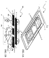
- FIG. 1A a first embodiment of an integrated sensor used in a alignment measurement system according to the present invention is schematically shown and generally indicated at 1.
- the integrated sensor 1 comprises a bottom die 3 including a plurality of bottom electrodes 5 surrounded by a guard ring 4 and overlaid by a top die 6 realising a top electrode 7.
- the bottom electrodes 5 comprise at least a top metal layer and are electrically insulated, by a dielectric or passivation layer (inter-chip medium), for instance silicon oxide, from the top electrode 7, which comprises at least a metal layer.
- a dielectric or passivation layer for instance silicon oxide
- the top electrode 7 does not completely overlap the lateral electrodes 5a and 5c.
- a multiple capacitors structure 2 is realised, a first C0, a second C1 and a third capacitor C2 being formed by the top 7 and bottom electrodes 5a, 5b and 5c, respectively, as indicated in Figure 1B which shows the principle of operation of the integrated sensor 1 of Figure 1A.
- the multiple capacitors structure 2 so obtained is used to encode a position information of chips assembled in a three-dimensional (3D) stacking configuration, the stacked device so realised being equipped and coupled by using at least an integrated sensor 1 as previously described.
- the bottom electrodes 5a, 5b, 5c are shown as having same width W and length L only for sake of simplicity, each of such bottom electrodes could have different values for the width and length parameters. So the bottom electrodes could be realised by different geometries (rectangles, rhombuses, circles, etc) or other material.
- an alignment measurement system 100 comprises a sensing circuit 8 has a first input terminal IN1 connected to a first terminal of the multiple capacitors structure 2, a second input terminal IN2 connected to a generator of a reference voltage Vref, a third input terminal IN3 receiving an input voltage Vin and an output terminal OUT also connected to a second terminal of the multiple capacitors structure 2.
- the sensing circuit 8 is an analog integrated read-out circuit.
- the first input terminal IN1 is connected to the bottom electrode 5b of the second capacitor C1
- the third input terminal IN3 is also connected to the bottom electrode 5a of the first capacitor C0
- the output terminal OUT is connected to the bottom electrode 5c of the third capacitor C2.
- the sensing circuit 8 comprises a differential amplifier 9 having a first input terminal corresponding to the first input terminal IN1, a second input terminal corresponding to the second input terminal IN2 and an output terminal corresponding to output terminal OUT.
- the bottom electrodes 5 are surrounded by the guard ring 4, which is a grounded electrode.
- the bottom electrodes 5 are realised as a comb of metal stripes with different sizes and pitches.
- an X/Y-Axis or lateral integrated sensor 1 is obtained in a simple and accurate manner
- the lateral integrated sensor 1 can be used to determine the misalignment between chips assembled in a three-dimensional (3D) stacking configuration, by properly connecting at least an integrated sensors 1 to the chips, a measure of the misalignment along X/Y axis could be thus simply obtained.
- the integrated sensor 1 within a top chip and to a bottom chip that have to be alignment, the top die 6 being integrate in the top chip and the bottom die 3 and the sensing circuit 8 being integrate in the bottom chip.
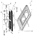
- FIG. 1 A second embodiment of an integrated sensor having a similar structure with respect to the integrated sensor 1 is schematically shown in Figure 2A and generally indicated at 10.
- the integrated sensor 10 is also used in an alignment measurement system according to the present invention.
- the integrated sensor 10 comprises a multiple capacitors structure 2, in this case in a three electrodes scheme.
- the integrated sensor 10 comprises a bottom die 3 including a plurality of bottom electrodes 5 surrounded by a guard ring 4 and overlaid by a top die 6 realising a top electrode 7.
- the bottom die 3 comprises two bottom electrodes 5a and 5b. It should be noted that the top electrode 7 fully overlaps the bottom electrodes 5a and 5b, so obtaining a two series-connected capacitors structure 2 and thus a three-electrode integrated sensor 10 able to measure alignment of stacked devices along Z-axis.
- the bottom electrodes 5a, 5b comprise at least a metal layer and are electrically insulated, by a dielectric or passivation layer, for instance silicon oxide, from the top electrode 7, which comprises at least a metal layer, in three dimensional configuration as above explained.
- a dielectric or passivation layer for instance silicon oxide
- the multiple capacitors structure 2 comprises a first C1 and a second capacitor C2 being formed by the top 7 and bottom electrodes 5a, 5b, respectively, as indicated in Figure 2B which shows the principle of operation of the integrated sensor 10 of Figure 2A.
- the integrated sensor 10 is connected to a sensing circuit 8a, in turn connected to the multiple capacitors structure 2.
- the sensing circuit 8a has a first input terminal IN1 connected to a first terminal of the multiple capacitors structure 2, a second input terminal IN2 connected to a generator of a reference voltage Vref, a third input terminal IN3 receiving an input voltage signal Vin (not shown) and an output terminal OUT also connected to a second terminal of the multiple capacitors structure 2.
- the sensing circuit 8a is a charge integrator.
- the generator of a reference voltage Vref can be provided by an internal or external source.
- the first input terminal IN1 is connected to the bottom electrode 5b of the first capacitor C1, and the output terminal OUT is connected to the bottom electrode 5c of the second capacitor C2.
- the first input terminal IN1 is also connected, through a reference capacitor Cin, to the third input terminal IN3.
- the sensing circuit 8a comprises a differential amplifier 9 having a first input terminal corresponding to the first input terminal IN1, a second input terminal corresponding to the second input terminal IN2 and an output terminal corresponding to the output terminal OUT.
- bottom electrodes 5a, 5b are connected separately to the first input terminal IN and to the output terminal OUT.
- the first and second capacitors C1, C2 of the multiple capacitors structure 2 are substantially a feedback capacitor structure for the differential amplifier 9 whose value Cz corresponds to the series of these first and second capacitors C1, C2 and the sensing circuit 8a is thus a charge integrator.
- the feedback capacitor Cz is inversely proportional to a vertical distance z between the top and bottom dies 6, 3 along a Z-axis direction (defined as a normal with respect to a plane of the integrated sensor 1, i.e., of the top 6 and bottom dies 3 thereof and shown in Figure 2A) while the output voltage Vout of the differential amplifier 9 is inversely proportional to the feedback capacitance value Cz, a linear dependence of output voltage Vout on the vertical distance d is so obtained.
- a Z-Axis or vertical integrated sensor 10 is obtained in a simple and accurate manner.
- the integrated sensor 10 can be used to determine the distance or separation between chips assembled in a three-dimensional (3D) stacking configuration, by properly connecting at least an integrated sensors 10 to the chips, a measure of the distance along a Z axis could be thus simply obtained.
- top die 6 being thus a top chip
- bottom die 3 being a bottom chip
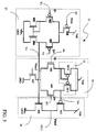
- a additional measurement system as shown in Figure 3, globally indicated at 20, can be used.
- the additional measurement system 20 comprises the sensing circuit 8 corresponding to one described with reference to Figures 1B.
- the sensing circuit 8 has a first input terminal IN1 connected to the lateral integrated sensor 1 and therefore to device under test 21, a second input terminal IN2 connected to a generator of a reference voltage Vref, a third input terminal IN3 connected to a generator of an input voltage Vin and an output terminal OUT, also connected to the device under test 21.
- the output terminal OUT of the sensing circuit 8 is also connected, through a first buffer 23, to a first output terminal OUT1 of the additional measurement system 20, such first output terminal OUT1 issuing a first output voltage signal Vout_Ext.
- the first output voltage signal Vout_Ext is proportional to the output voltage Vout of the sensing circuit 8, which is proportional to the input voltage Vin and to the capacitive value of the multiple capacitors structure 2.
- the first output voltage signal Vout_Ext is a measure of the displacement between electrodes of the integrated sensors of the device under test 21.
- the additional measurement system 20 comprises a sum amplifier 24 having a first input terminal connected, through a series of a second buffer 25 and a first resistor R1 to the generator of the input voltage Vin, a second input terminal connected to the generator of the reference voltage Vref and an output terminal connected to a second output terminal OUT2 of the additional alignment measurement system 20, such second output terminal OUT2 issuing a second output voltage signal Vout_Sum.
- the sum amplifier 24 can be formed by other circuit 24 able to determine the amplitude of the output voltage of sensing circuit Vout (for example an analog multipliers).
- the second output terminal OUT2 is used to feed data back to an external manipulator to validate and compare the alignment information obtained by the additional measurement system 20.
- the output terminal of the sum amplifier 24 is also connected to its first input terminal by means of a second resistor R2 and to the output terminal OUT of the sensing circuit 8 through a series of the second resistor R2, of a third resistor R3 and of a third buffer 26.
- first Vout_Ext and second output voltage signals Vout_Sum are derived from the output voltage Vout issued from the output terminal OUT of the differential amplifier 9. It should be remarked that the output voltage Vout is in turn proportional to the charge variation of the multiple capacitors structure 2. So, the first output voltage signal has the information about the direction of the displacement while the second output voltage signal Vout_sum provides the entity of the displacement.
- the summing amplifier 24 feeds back the second output voltage signal Vout_Sum to an off-chip micromanipulator (not shown in the figures) that drives known placement machines, thus creating a closed-loop for a precise placement of the chips in the three-dimensional (3D) stacking configuration of the stacked device.
- the sensing circuit 8 should be differently configured whether the stacked device under test 21 is equipped with a lateral integrated sensor 1 or with a vertical integrated sensor 10.
- the sensing circuit 8 is a low impedance AC read-out circuit, as shown in Figure 4A.
- the sensing circuit 8 comprises a differential amplifier 9 connected to the multiple capacitors structure 2.
- the sensing circuit 8 has a first input terminal IN1 connected to the multiple capacitors structure 2, in particular to a first end of the second capacitor C1 having in turn a second end connected, at a central node Xc, to a first end of the third capacitor C2, which has a second end connected to the output terminal OUT of the sensing circuit 8.
- the sensing circuit 8 also has a third input terminal IN3 connected to the generator of the input voltage Vin and to the multiple capacitors structure 2, in particular to a first end of the first capacitor C0, having in turn a second end connected, at the central node Xc, to the second end of the second capacitor C1 as well as to the first end of the third capacitor C2.
- the output terminal OUT issues the output voltage Vout.
- the differential amplifier 9 comprises an operational amplifier 27 cascade-connected to an output stage 28, as shown in Figure 4A.
- the operational amplifier 27 is inserted between a first and a second voltage reference, in particular a supply voltage reference Vdd and a ground GND, and has a first input terminal Y1 connected to first input terminal IN1 of the sensing circuit 8, in turn connected to a generator of a reference voltage Vref by means of a switch SW1.
- the operational amplifier 27 also has a second input terminal Y2 connected to the generator of the reference voltage Vref and the second input terminal IN2.
- the operational amplifier 27 has a first Y3 and a second output terminal Y4 connected to the output stage 28.
- the operational amplifier 27 comprises a first M1 and a second transistor M2 connected to the ground GND by respectively third M3 and fourth transistor M4 and to the supply voltage reference Vdd by means of a bias transistor M0, having a control or gate terminal connected to a generator of a bias voltage Vbias.
- the first transistor M1 has a first conduction terminal connected to the bias transistor M0 and a second conduction terminal connected to a first conduction terminal of the third transistor M3, having in turn a second conduction terminal connected to ground GND.
- the first transistor M1 has a control or gate terminal connected to the first input terminal Y1 of the operational amplifier 27.
- the second transistor M2 has a first conduction terminal in common with the first conduction terminal of the first transistor M1 and connected to the bias transistor M0 and a second conduction terminal connected to a first conduction terminal of the fourth transistor M4, having in turn a second conduction terminal connected to ground GND.
- the second transistor M2 has a control or gate terminal connected to the second input terminal Y2 of the operational amplifier 27.
- the third M3 and fourth transistor M4 have the control or gate terminals connected to each other, the third transistor M3 being diode-connected.
- the gate terminal of the bias transistor M0 is connected to a first output terminal Y3 of the operational amplifier 27 and the second conduction terminal of the second transistor M2, which is connected to the first conduction terminal of the fourth transistor M4, is also connected to a second output terminal Y4 of the operational amplifier 27.
- the output stage 28 comprises a fifth M5 and a sixth transistor M6 which are series-connected between the supply voltage reference Vdd and ground GND.
- the fifth transistor M5 has a first conduction terminal connected to the supply voltage reference Vdd and a second conduction terminal connected to a first conduction terminal of the sixth transistor M6, having in turn a second conduction terminal connected to ground GND.
- the fifth transistor M5 has a control or gate terminal connected to the first output terminal Y3 of the operational amplifier 27 and the sixth transistor M6 has a control or gate terminal connected to the second output terminal Y4 of the operational amplifier 27.
- the second conduction terminal of the fifth transistor M5, which is connected to the first conduction terminal of the sixth transistor M6, is also connected to the output terminal OUT of the sensing circuit 8.
- Vout is computed by means of the charge conservation principle. Assuming that the operational amplifier 27 is in virtual ground and infinite gain condition, the following equation can be derived: Vout ⁇ - C ⁇ 0 C ⁇ 2 ⁇ Vin + Co + C ⁇ 2 C ⁇ 2 ⁇ Vref
- a charge variation 8Q is induced on the second capacitor C1, i.e, on the central electrode 5b.
- This charge variation ⁇ Q is detected by the operational amplifier 27 and, due to the feedback loop realised by connecting the output terminal OUT to the multiple capacitors structure 2, it produces a corresponding charge variation on the third capacitor C2, i.e. on the third electrode 5c which acts as a pick-up electrode.
- the output voltage Vout is thus a sinusoidal waveform proportional to a C0/C2 ratio and with opposite phase with respect to the input sinusoidal signal Vin.
- a on-chip generated or external analog reference level Vref is provide to the amplifier and buffer of alignment measurement system 20.
- the sine wave input voltage Vin should have a frequency equal to 1MHz in order to obtain a voltage reference Vref equal to Vdd/2.
- a gain of 42dB is achieved by the operational amplifier 27.
- the switch SW1 allows to pre-charge and to reset the first input terminal X1 to a fixed bias voltage value, equal to the voltage reference Vref, during a measurement performed by the alignment measurement system 100 to avoid saturation of the amplifier circuits 8.
- the operational amplifier 27 is a low impedance AC high gain amplifier.
- the alignment measurement system 100 comprising the sensing circuit 8 has better performance with low voltage rails because of a better common mode range of the operational amplifier 27 that can thus be used to linearise the output voltage signal Vout.
- the sensing circuit 8a is a charge voltage sensing amplifier, as shown in Figure 4B.
- the sensing circuit 8a comprises a differential amplifier 9 connected to the multiple capacitors structure 2.
- the sensing circuit 8a has a first input terminal IN 1 connected to the multiple capacitors structure 2, in particular to a first end of the first capacitor C1, having in turn a second end connected to a first end of the second capacitor C2 which has a second end connected to the output terminal OUT.
- the sensing circuit 8a also has a first input terminal IN1 connected, by means of a switch SW1, to the generator of the reference voltage Vref and, though the input capacitor Cin, to the third input terminal IN3, in turn connected to the generator of the input voltage Vin.
- the output terminal OUT issues the output voltage Vout.
- the differential amplifier 9 comprises an operational amplifier 27 cascade-connected to an output stage 28.
- the Cz is inversely dependent on the vertical distance between the electrodes of the vertical integrated sensor 10, i.e. between two chips of a stacked device, the chips being equipped with the vertical integrated sensor 10.
- the transistors M2, M3, M4 and M5 are NMOS and the transistors M0, M1 and M6 are PMOS.
- the first buffer 23 is configured as a unity gain buffer by comprising an operation amplifier 27 and a output stage 28 as the differential amplifier 9, as well as an intermediate block 30, as shown in Figure 5.
- the intermediate block 30 is inserted between the supply voltage reference Vdd and ground GND and has a first input terminal Y6 connected to the first input terminal Y1 of the operational amplifier 27, a second input terminal Y7 connected to the second input terminal Y2 of the operational amplifier 27 and an output terminal Y8 connected to the output stage 28, in particular to the gate terminal of the fifth transistor M5 of the output stage 28, while the gate terminal of the sixth transistor M6 of the output stage 28 is connected to the second output terminal Y4 of the operational amplifier 27.
- the intermediate block 30 comprises a first transistor M8 having a first conduction terminal connected, through a mirror block 31, to the supply voltage reference Vdd, a second conduction terminal connected, through a bias transistor M7, to ground GND and a control or gate terminal connected to first input terminal Y6.
- the intermediate block 30 also comprises a second transistor M9 having a first conduction terminal connected, through the mirror block 31, to the supply voltage reference Vdd, a second conduction terminal connected to the second conduction terminal of the first transistor M8 and, through the bias transistor M7, to ground GND and a control or gate terminal connected to second input terminal Y7.
- the first and second transistors M8 and M9 of the intermediate block 30 substantially form a differential cell.
- the first conduction terminal of the second transistor M9 is also connected to the output terminal Y8 of the intermediate block 30.
- the bias transistor M7 has a first conduction terminal connected to the second conduction terminals of the first and second transistors M8 and M9, a second conduction terminal connected to ground GND and a control or gate terminal connected to a generator of a second bias voltage Vbias2.
- the mirror block 31 comprises a third transistor M10 having a first conduction terminal connected to the supply voltage reference Vdd, a second conduction terminal connected to the first conduction terminal of the first transistor M8 of the intermediate block 30 and a control or gate terminal connected to a control or gate terminal of a fourth transistor M11, having in turn a first conduction terminal connected to the supply voltage reference Vdd and a second conduction terminal connected to the first conduction terminal of the second transistor M9 of the intermediate block 30, the third transistor M10 being diode-connected.
- the transistors M7, M8 and M9 are NMOS and the transistors M 10 and M11 are PMOS.
- the differential amplifier 9 correctly provides external pins with the output voltage Vout for testing, the external pins being connected to the first output terminal OUT1 of the alignment measurement system 100.
- the unity gain buffer configuration of the differential amplifier 9 with the intermediate block 30 is able to drive external pins.
- an AC input signal Vin having a sine-wave is used, this kind of signal allowing simplified comparison between applied and measured values and it allows to filter the noise and to have better performance in term of the signal to noise ratio.
- the size of electrodes for the integrated sensors are 120 ⁇ m x 30 ⁇ m.
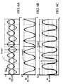
- Figure 6B shows a measured output voltage Voutm2 in a perfect alignment condition (plot S2) of the upper 7 and bottom electrodes 5 of an integrated sensor 1.
- the capacitance value C0 and C2 of the multiple capacitors structure 2 are the same, the differential amplifier 9 works like a buffer, and, as a result, the measured output voltage Voutm2 has the same amplitude of the input voltage Vin.
- Figure 6A shows a measured output voltage Voutm1 in case of a right displacement along one direction (plot S1) and Figure 6C shows a measured output voltage Voutm3 in case of a left displacements along one direction (plot S3).
- the measured output voltage Voutm3 which is a sinusoidal waveform, has a bigger amplitude than the input voltage Vin, since the first capacitor C0 value is greater than the third capacitor C2 value.
- the measured output voltage Voutm1 which is a sinusoidal waveform, has a lower amplitude than the input voltage Vin, since the first capacitor C0 value is less than the third capacitor C2.
- the entity as well as the direction of the measured displacement are derived.
- a four-electrode sensor 1 has been distributed along the perimeter on the chip plane to detect position information on X and Y direction, while three-electrode sensors 10 have been located in the four corners of the chip to enable measure of displacement in Z direction and also to provide tilt, as shown in Figure 7.
- a combination of four-electrode sensors 1 and three-electrode sensors 10, on the chip plane, is also enabled to measure of displacement related to the rotation.
- the alignment measurement system 100, 1001 allows to measure displacement in the X, Y, Z directions between chips assembled in a three-dimensional (3D) stacking configuration having a greater precision with respect to the known measurement devices.
- the alignment measurement system 100, 101 according to the present invention make it possible to perform measurements at an early stage of packaging because the top chip does not need any power supply.
- the alignment measurement system 100, 101 is able to measure a post-bonding accuracy and feeds data back to the external manipulator to validate and compare the alignment information.
Landscapes
- Engineering & Computer Science (AREA)
- Computer Hardware Design (AREA)
- Microelectronics & Electronic Packaging (AREA)
- General Engineering & Computer Science (AREA)
- Physics & Mathematics (AREA)
- General Physics & Mathematics (AREA)
- Semiconductor Integrated Circuits (AREA)
- Measurement Of Length, Angles, Or The Like Using Electric Or Magnetic Means (AREA)
Abstract
- a multiple capacitors structure (2) integrated in said capacitive sensor (1, 10)
- at least a sensing circuit (8, 8a) connected to said multiple capacitors structure (2) which issues an output voltage (Vout), proportional to a variation of a capacitive value of the multiple capacitors structure (2) of the integrated capacitive sensor (1, 10) of the device under test (21) and corresponding to a measured misalignment between the chips of the device under test (21).

Description
- The present invention relates to an alignment measurement system to determine alignment between chips.
- More specifically, the invention relates to an alignment measurement system for measuring alignment between a plurality of chips of a device under test, the chips being assembled in a three-dimensional stacking configuration and equipped with at least an integrated capacitive sensor, the system being inserted between a first and a second voltage references and connected to the device under test.
- As it is well known, the development of stacking technology for heterogeneous device integration has recently increased in importance.
- Stacking of chips, in which two or more integrated circuits or ICs of different types are placed one on the top of the other in a same package, is an alternative to silicon integration and provides improvements at the system design level in terms of size, cost, speed, power consumption and ease of application for a wide variety of products.
- However, successful implementation of the stacking or 3D technology requires dealing with state-of-the-art of assembly processes such as wafer back-grinding, handling, die attach, wirebond and alignment. So, the choice of a stacking or 3D technology depends largely on the application of the final chip so obtained.
- In particular, vertical data communication using AC wireless interconnect has been recently presented as very promising stacking or 3D technology for high-bandwidth, high speed applications, as described in the article to Kanda K. et al. entitled "1.27Gb/s/pin 3mW/pin wireless superconnect wsc interface scheme", ISSCC Dig. Tech. Papers, pp. 186-187, Feb 2003.
- In this field of application, in order to improve the inter-chip communication efficiency, a very accurate and precise alignment of the stacked chips is required.
- Many strategies have been presented to make chip positioning with sub-micron precision possible. Known alignment systems and methods allowing a sub-micron precision are described for instance in the following articles:
- Neville K. S Lee, "An-Ultra precision alignment system for Micro-machining", IEEE ICIT 2002;
- M. Olson et al, "Sub-micrometer precision measurement method for wafer level assembly", International Conference on Solid State Sensors, Actuators and Microsystem June 2003; and
- R. J. Drost et al., "Electronic Alignment for Proximity Communication", ISSCC Dig. Tech. Papers, pp. 144-145, Feb 2004.
- Also known from the
US Patent No. 4,566,193 issued on January 28, 1986 in the name of Hackleman et al. (Hewlett-Packard Company) is an electronic vernier which detects and quantifies misalignment between layers of deposited material on a semiconducting wafer, in particular during a semiconductor manufacturing process. - Furthermore, the
US Patent No. 6,518,679 issued on February 11, 2003 in the name of Lu et al. (IBM Corporation) describes a capacitive alignment structure and method for chip stacking. - Some of these known approaches require expensive and complex servomechanisms, sensors and actuators. Moreover, the methods and systems actually available in the field are not standard but tailored to a specific application of a final stacked device to be realised.
- The technical problem underlying the present invention is that of providing a system for measuring alignment between chips, in particular assembled in a three-dimensional (3D) stacking configuration, having structural and functional characteristics which allow a sub-micron precision in measuring chip positioning without requiring expensive and complex components, in this way overcoming the limits which still affect the systems realised according to the prior art.
- The solution idea underlying the present invention is that of associate to at least an integrated CMOS capacitive sensor connected to the chips comprised in a three-dimensional (3D) stacking configuration a sensing circuit to provide an on-chip measurement of a stacked configuration alignment along vertical Z-axis or lateral X/Y-axis.
- On the basis of such solution idea the technical problem is solved by an alignment measurement system as previously indicated and defined by the characterising part of
claim 1. - The characteristics and advantages of the system according to the invention will be apparent from the following description of embodiments thereof given by way of indicative and non limiting example with reference to the annexed drawings.
- In the drawings:
- Figures 1A and 1B schematically show a cross section of a first embodiment of an alignment measurement system according to the present invention and its sensing principle, respectively;
- Figures 2A and 2B schematically show a cross section of a second embodiment of an alignment measurement system according to the present invention and its sensing principle, respectively;
- Figure 3 diagrammatically shows an additional measurement system according to the present invention;
- Figure 4A schematically shows details of the system of Figure 1B,
- Figure 4B schematically shows details of the system of Figure 2B,
- Figure 5 schematically shows details of the system of Figure 3;
- Figures 6A-6C schematically show measured signal waveforms of the system of Figure 3;
- Figures 7A-7B schematically show a multi axis sensors distribution used by the alignment measurement system according to the present invention.
- The use of integrated capacitive sensors promises to meet the demand for low-cost, high resolution, high-reproducibility measurement systems.
- With reference to the figures, and in particular to Figures 1A and 1B, a first embodiment of an integrated sensor used in a alignment measurement system according to the present invention is schematically shown and generally indicated at 1.
- The integrated
sensor 1 comprises abottom die 3 including a plurality ofbottom electrodes 5 surrounded by aguard ring 4 and overlaid by atop die 6 realising a top electrode 7. - In particular, in the example shown in Figure 1A, the bottom die 3 comprises three
bottom electrodes sensor 1 able to measure alignment of stacked devices along X or Y-axis. - Generally, the
bottom electrodes 5 comprise at least a top metal layer and are electrically insulated, by a dielectric or passivation layer (inter-chip medium), for instance silicon oxide, from the top electrode 7, which comprises at least a metal layer. - In other words, the top and bottom electrodes or dies are stacked together in a three-dimensional configuration (with respect to the metal i.e. conductive layer) and the passivation layer of silicon oxide is used as dielectric to build a capacitor.
- Advantageously in this embodiment the top electrode 7 does not completely overlap the
lateral electrodes - In this way, a
multiple capacitors structure 2 is realised, a first C0, a second C1 and a third capacitor C2 being formed by the top 7 andbottom electrodes sensor 1 of Figure 1A. As it will be clear from the following description, themultiple capacitors structure 2 so obtained is used to encode a position information of chips assembled in a three-dimensional (3D) stacking configuration, the stacked device so realised being equipped and coupled by using at least an integratedsensor 1 as previously described. Assuming a parallel plate model, wherein the capacitor plates are thebottom electrodes multiple capacitors structure 2 is then calculated from the equation:
where: - ε0 is the dielectric constant in vacuum
- εr is the permittivity of the inter-chip medium
- W is a width of each
bottom electrodes - L is a length of each
bottom electrodes - d is a distance between the
bottom electrodes - In Figure 1A, the
bottom electrodes - It is clear that a shift or displacement of the top electrode 7, along X or Y axis direction (defined with respect to a plane of the integrated
sensor 1, i.e., of thetop 6 andbottom die 3 thereof and shown in Figure 1A) changes an overlapping area defined by the top electrode 7 and each of thebottom electrodes multiple capacitors structure 2 according to the above equation (1). - In particular, according to a first embodiment of an
alignment measurement system 100 according to the invention as shown in Figure 1B, comprises asensing circuit 8 has a first input terminal IN1 connected to a first terminal of themultiple capacitors structure 2, a second input terminal IN2 connected to a generator of a reference voltage Vref, a third input terminal IN3 receiving an input voltage Vin and an output terminal OUT also connected to a second terminal of themultiple capacitors structure 2. Thesensing circuit 8 is an analog integrated read-out circuit. - In particular, the first input terminal IN1 is connected to the
bottom electrode 5b of the second capacitor C1, the third input terminal IN3 is also connected to thebottom electrode 5a of the first capacitor C0 and the output terminal OUT is connected to thebottom electrode 5c of the third capacitor C2. - The
sensing circuit 8 comprises adifferential amplifier 9 having a first input terminal corresponding to the first input terminal IN1, a second input terminal corresponding to the second input terminal IN2 and an output terminal corresponding to output terminal OUT. - In order to encode the position information of chips assembled in a three-dimensional (3D) stacking configuration, the
sensing circuit 8 issues an output voltage Vout which is proportional to the input voltage Vin according to the following equation:
- If the chips are aligned, C0 is equal to C2, therefore the output voltage Vout is equal with an opposite phase with respect to the input voltage Vin. If the chips are misaligned, C0 is different from C2, therefore the output voltage Vout is greater or smaller than the input voltage Vin. So it is possible detected in which direction chips are shifted along the X or Y axis,
- Advantageously, in order to reduce the electric-field bending effect and the external interference, the
bottom electrodes 5 are surrounded by theguard ring 4, which is a grounded electrode. - Also advantageously, to compute coarse and fine alignment measurement, the
bottom electrodes 5 are realised as a comb of metal stripes with different sizes and pitches. - So, an X/Y-Axis or lateral
integrated sensor 1 is obtained in a simple and accurate manner, The lateralintegrated sensor 1 can be used to determine the misalignment between chips assembled in a three-dimensional (3D) stacking configuration, by properly connecting at least anintegrated sensors 1 to the chips, a measure of the misalignment along X/Y axis could be thus simply obtained. - It is also possible to embed the
integrated sensor 1 within a top chip and to a bottom chip that have to be alignment, the top die 6 being integrate in the top chip and the bottom die 3 and thesensing circuit 8 being integrate in the bottom chip. - In this case, it should be noted that, advantageously according to the invention, by using the above described four-electrode integrated
sensor 1 along with thesensing circuit 8, it is not necessary that the top chip is powered. - A second embodiment of an integrated sensor having a similar structure with respect to the
integrated sensor 1 is schematically shown in Figure 2A and generally indicated at 10. Theintegrated sensor 10 is also used in an alignment measurement system according to the present invention. - For sake of clarity, the same reference numbers will be used to indicate parts of the
integrated sensor 10 which structurally and/or functionally correspond to the ones described with reference to theintegrated sensor 1 shown Figures 1A and 1B. - So, the
integrated sensor 10 comprises amultiple capacitors structure 2, in this case in a three electrodes scheme. - In particular, the
integrated sensor 10 comprises abottom die 3 including a plurality ofbottom electrodes 5 surrounded by aguard ring 4 and overlaid by atop die 6 realising a top electrode 7. - In this case, as shown in Figure 2A, the bottom die 3 comprises two
bottom electrodes bottom electrodes capacitors structure 2 and thus a three-electrode integratedsensor 10 able to measure alignment of stacked devices along Z-axis. - As previously described, in a preferred embodiment, the
bottom electrodes - The
multiple capacitors structure 2 comprises a first C1 and a second capacitor C2 being formed by the top 7 andbottom electrodes integrated sensor 10 of Figure 2A. - In second embodiment of an
alignment measurement system 101 according to the invention ,theintegrated sensor 10 is connected to asensing circuit 8a, in turn connected to themultiple capacitors structure 2. In particular, thesensing circuit 8a has a first input terminal IN1 connected to a first terminal of themultiple capacitors structure 2, a second input terminal IN2 connected to a generator of a reference voltage Vref, a third input terminal IN3 receiving an input voltage signal Vin (not shown) and an output terminal OUT also connected to a second terminal of themultiple capacitors structure 2. In this case, thesensing circuit 8a is a charge integrator. - The generator of a reference voltage Vref can be provided by an internal or external source.
- In particular, the first input terminal IN1 is connected to the
bottom electrode 5b of the first capacitor C1, and the output terminal OUT is connected to thebottom electrode 5c of the second capacitor C2. - The first input terminal IN1 is also connected, through a reference capacitor Cin, to the third input terminal IN3.
- The
sensing circuit 8a comprises adifferential amplifier 9 having a first input terminal corresponding to the first input terminal IN1, a second input terminal corresponding to the second input terminal IN2 and an output terminal corresponding to the output terminal OUT. - It should be noted that the
bottom electrodes - In this way, the first and second capacitors C1, C2 of the
multiple capacitors structure 2 are substantially a feedback capacitor structure for thedifferential amplifier 9 whose value Cz corresponds to the series of these first and second capacitors C1, C2 and thesensing circuit 8a is thus a charge integrator. - So, the
sensing circuit 8a issues an output voltage Vout whose differential ΔVout is proportional to a differential ΔVin of the input voltage Vin according to the following equation:

- Since the feedback capacitor Cz is inversely proportional to a vertical distance z between the top and bottom dies 6, 3 along a Z-axis direction (defined as a normal with respect to a plane of the
integrated sensor 1, i.e., of the top 6 and bottom dies 3 thereof and shown in Figure 2A) while the output voltage Vout of thedifferential amplifier 9 is inversely proportional to the feedback capacitance value Cz, a linear dependence of output voltage Vout on the vertical distance d is so obtained. - So, a Z-Axis or vertical
integrated sensor 10 is obtained in a simple and accurate manner. Theintegrated sensor 10 can be used to determine the distance or separation between chips assembled in a three-dimensional (3D) stacking configuration, by properly connecting at least anintegrated sensors 10 to the chips, a measure of the distance along a Z axis could be thus simply obtained. - It is also possible to embed the
integrated sensor 10 on the chips themselves, the top die 6 being thus a top chip and the bottom die 3 being a bottom chip. - Advantageously according to the invention, by using lateral
integrated sensors 1 as previously described, a additional measurement system, as shown in Figure 3, globally indicated at 20, can be used. - Advantageously according to the invention, the
additional measurement system 20 comprises thesensing circuit 8 corresponding to one described with reference to Figures 1B. - As previously described with reference to Figures 1B, the
sensing circuit 8 has a first input terminal IN1 connected to the lateralintegrated sensor 1 and therefore to device undertest 21, a second input terminal IN2 connected to a generator of a reference voltage Vref, a third input terminal IN3 connected to a generator of an input voltage Vin and an output terminal OUT, also connected to the device undertest 21. - In particular, the output terminal OUT of the
sensing circuit 8 is also connected, through afirst buffer 23, to a first output terminal OUT1 of theadditional measurement system 20, such first output terminal OUT1 issuing a first output voltage signal Vout_Ext. - In this way, the first output voltage signal Vout_Ext is proportional to the output voltage Vout of the
sensing circuit 8, which is proportional to the input voltage Vin and to the capacitive value of themultiple capacitors structure 2. In other words, the first output voltage signal Vout_Ext is a measure of the displacement between electrodes of the integrated sensors of the device undertest 21. - Furthermore, the
additional measurement system 20 comprises asum amplifier 24 having a first input terminal connected, through a series of asecond buffer 25 and a first resistor R1 to the generator of the input voltage Vin, a second input terminal connected to the generator of the reference voltage Vref and an output terminal connected to a second output terminal OUT2 of the additionalalignment measurement system 20, such second output terminal OUT2 issuing a second output voltage signal Vout_Sum. - Nothing prevents that the
sum amplifier 24 can be formed byother circuit 24 able to determine the amplitude of the output voltage of sensing circuit Vout (for example an analog multipliers). - Advantageously, the second output terminal OUT2 is used to feed data back to an external manipulator to validate and compare the alignment information obtained by the
additional measurement system 20. - The output terminal of the
sum amplifier 24 is also connected to its first input terminal by means of a second resistor R2 and to the output terminal OUT of thesensing circuit 8 through a series of the second resistor R2, of a third resistor R3 and of athird buffer 26. - In particular the first Vout_Ext and second output voltage signals Vout_Sum are derived from the output voltage Vout issued from the output terminal OUT of the
differential amplifier 9. It should be remarked that the output voltage Vout is in turn proportional to the charge variation of themultiple capacitors structure 2. So, the first output voltage signal has the information about the direction of the displacement while the second output voltage signal Vout_sum provides the entity of the displacement. - It should be noted that, advantageously according to the present invention, the summing
amplifier 24 feeds back the second output voltage signal Vout_Sum to an off-chip micromanipulator (not shown in the figures) that drives known placement machines, thus creating a closed-loop for a precise placement of the chips in the three-dimensional (3D) stacking configuration of the stacked device. - As previously explained, the
sensing circuit 8 should be differently configured whether the stacked device undertest 21 is equipped with a lateralintegrated sensor 1 or with a verticalintegrated sensor 10. - Advantageously, when the stacked device under
test 21 comprises lateralintegrated sensors 1, thesensing circuit 8 is a low impedance AC read-out circuit, as shown in Figure 4A. - As already explained with reference to Figure 1B, the
sensing circuit 8 comprises adifferential amplifier 9 connected to themultiple capacitors structure 2. - In particular, the
sensing circuit 8 has a first input terminal IN1 connected to themultiple capacitors structure 2, in particular to a first end of the second capacitor C1 having in turn a second end connected, at a central node Xc, to a first end of the third capacitor C2, which has a second end connected to the output terminal OUT of thesensing circuit 8. - The
sensing circuit 8 also has a third input terminal IN3 connected to the generator of the input voltage Vin and to themultiple capacitors structure 2, in particular to a first end of the first capacitor C0, having in turn a second end connected, at the central node Xc, to the second end of the second capacitor C1 as well as to the first end of the third capacitor C2. The output terminal OUT issues the output voltage Vout. - Advantageously according to the present invention, the
differential amplifier 9 comprises anoperational amplifier 27 cascade-connected to anoutput stage 28, as shown in Figure 4A. - In particular, the
operational amplifier 27 is inserted between a first and a second voltage reference, in particular a supply voltage reference Vdd and a ground GND, and has a first input terminal Y1 connected to first input terminal IN1 of thesensing circuit 8, in turn connected to a generator of a reference voltage Vref by means of a switch SW1. Theoperational amplifier 27 also has a second input terminal Y2 connected to the generator of the reference voltage Vref and the second input terminal IN2. - Furthermore, the
operational amplifier 27 has a first Y3 and a second output terminal Y4 connected to theoutput stage 28. - The
operational amplifier 27 comprises a first M1 and a second transistor M2 connected to the ground GND by respectively third M3 and fourth transistor M4 and to the supply voltage reference Vdd by means of a bias transistor M0, having a control or gate terminal connected to a generator of a bias voltage Vbias. - In particular, the first transistor M1 has a first conduction terminal connected to the bias transistor M0 and a second conduction terminal connected to a first conduction terminal of the third transistor M3, having in turn a second conduction terminal connected to ground GND.
- The first transistor M1 has a control or gate terminal connected to the first input terminal Y1 of the
operational amplifier 27. - In an analogous manner, the second transistor M2 has a first conduction terminal in common with the first conduction terminal of the first transistor M1 and connected to the bias transistor M0 and a second conduction terminal connected to a first conduction terminal of the fourth transistor M4, having in turn a second conduction terminal connected to ground GND.
- The second transistor M2 has a control or gate terminal connected to the second input terminal Y2 of the
operational amplifier 27. - Also, the third M3 and fourth transistor M4 have the control or gate terminals connected to each other, the third transistor M3 being diode-connected.
- Finally, the gate terminal of the bias transistor M0 is connected to a first output terminal Y3 of the
operational amplifier 27 and the second conduction terminal of the second transistor M2, which is connected to the first conduction terminal of the fourth transistor M4, is also connected to a second output terminal Y4 of theoperational amplifier 27. - Moreover, the
output stage 28 comprises a fifth M5 and a sixth transistor M6 which are series-connected between the supply voltage reference Vdd and ground GND. - In particular, the fifth transistor M5 has a first conduction terminal connected to the supply voltage reference Vdd and a second conduction terminal connected to a first conduction terminal of the sixth transistor M6, having in turn a second conduction terminal connected to ground GND.
- Also, the fifth transistor M5 has a control or gate terminal connected to the first output terminal Y3 of the
operational amplifier 27 and the sixth transistor M6 has a control or gate terminal connected to the second output terminal Y4 of theoperational amplifier 27. - Finally, the second conduction terminal of the fifth transistor M5, which is connected to the first conduction terminal of the sixth transistor M6, is also connected to the output terminal OUT of the
sensing circuit 8. - In this way, the output voltage Vout is computed by means of the charge conservation principle. Assuming that the
operational amplifier 27 is in virtual ground and infinite gain condition, the following equation can be derived:
- Considering as input voltage Vin a sinusoidal signal applied to one end of the first capacitor C0, and thus to the
first electrode 5a of theintegrated sensor 1, a charge variation 8Q is induced on the second capacitor C1, i.e, on thecentral electrode 5b. - This charge variation δQ is detected by the
operational amplifier 27 and, due to the feedback loop realised by connecting the output terminal OUT to themultiple capacitors structure 2, it produces a corresponding charge variation on the third capacitor C2, i.e. on thethird electrode 5c which acts as a pick-up electrode. - According to the above equation (4), the output voltage Vout is thus a sinusoidal waveform proportional to a C0/C2 ratio and with opposite phase with respect to the input sinusoidal signal Vin.
- Advantageously according to the invention, a on-chip generated or external analog reference level Vref, is provide to the amplifier and buffer of
alignment measurement system 20. - In an embodiment of the invention considering a single power supply voltage Vdd of 1.2 Volt, the sine wave input voltage Vin should have a frequency equal to 1MHz in order to obtain a voltage reference Vref equal to Vdd/2.
- For example, using a bias current of 10µA, a gain of 42dB is achieved by the
operational amplifier 27. - The switch SW1 allows to pre-charge and to reset the first input terminal X1 to a fixed bias voltage value, equal to the voltage reference Vref, during a measurement performed by the
alignment measurement system 100 to avoid saturation of theamplifier circuits 8. - Advantageously according to the invention, the
operational amplifier 27 is a low impedance AC high gain amplifier. In this way, thealignment measurement system 100 comprising thesensing circuit 8 has better performance with low voltage rails because of a better common mode range of theoperational amplifier 27 that can thus be used to linearise the output voltage signal Vout. - In a similar manner, when the stacked device under
test 21 comprises verticalintegrated sensors 10, thesensing circuit 8a is a charge voltage sensing amplifier, as shown in Figure 4B. - As already explained with reference to Figure 2B, the
sensing circuit 8a comprises adifferential amplifier 9 connected to themultiple capacitors structure 2. - In particular, the
sensing circuit 8a has a first input terminal IN 1 connected to themultiple capacitors structure 2, in particular to a first end of the first capacitor C1, having in turn a second end connected to a first end of the second capacitor C2 which has a second end connected to the output terminal OUT. Thesensing circuit 8a also has a first input terminal IN1 connected, by means of a switch SW1, to the generator of the reference voltage Vref and, though the input capacitor Cin, to the third input terminal IN3, in turn connected to the generator of the input voltage Vin. The output terminal OUT issues the output voltage Vout. - As already explained with reference to Figure 4A, the
differential amplifier 9 comprises anoperational amplifier 27 cascade-connected to anoutput stage 28. - In this case, the charge amplifier realised by the
sensing circuit 8a issues an output voltage Vout computed as:

- As above explained, the Cz is inversely dependent on the vertical distance between the electrodes of the vertical
integrated sensor 10, i.e. between two chips of a stacked device, the chips being equipped with the verticalintegrated sensor 10. - In the examples shown in Figures 4A and 4B, the transistors M2, M3, M4 and M5 are NMOS and the transistors M0, M1 and M6 are PMOS.
- In a preferred embodiment of the invention, the
first buffer 23 is configured as a unity gain buffer by comprising anoperation amplifier 27 and aoutput stage 28 as thedifferential amplifier 9, as well as anintermediate block 30, as shown in Figure 5. - For sake of clarity, the same reference numbers will be used to indicate parts of the
first buffer 23 which structurally and/or functionally correspond to the ones described with reference to thedifferential amplifier 9 shown Figures 4A and 4B. - The
intermediate block 30 is inserted between the supply voltage reference Vdd and ground GND and has a first input terminal Y6 connected to the first input terminal Y1 of theoperational amplifier 27, a second input terminal Y7 connected to the second input terminal Y2 of theoperational amplifier 27 and an output terminal Y8 connected to theoutput stage 28, in particular to the gate terminal of the fifth transistor M5 of theoutput stage 28, while the gate terminal of the sixth transistor M6 of theoutput stage 28 is connected to the second output terminal Y4 of theoperational amplifier 27. - In particular, the
intermediate block 30 comprises a first transistor M8 having a first conduction terminal connected, through amirror block 31, to the supply voltage reference Vdd, a second conduction terminal connected, through a bias transistor M7, to ground GND and a control or gate terminal connected to first input terminal Y6. - The
intermediate block 30 also comprises a second transistor M9 having a first conduction terminal connected, through themirror block 31, to the supply voltage reference Vdd, a second conduction terminal connected to the second conduction terminal of the first transistor M8 and, through the bias transistor M7, to ground GND and a control or gate terminal connected to second input terminal Y7. - The first and second transistors M8 and M9 of the
intermediate block 30 substantially form a differential cell. - The first conduction terminal of the second transistor M9 is also connected to the output terminal Y8 of the
intermediate block 30. - The bias transistor M7 has a first conduction terminal connected to the second conduction terminals of the first and second transistors M8 and M9, a second conduction terminal connected to ground GND and a control or gate terminal connected to a generator of a second bias voltage Vbias2.
- The
mirror block 31 comprises a third transistor M10 having a first conduction terminal connected to the supply voltage reference Vdd, a second conduction terminal connected to the first conduction terminal of the first transistor M8 of theintermediate block 30 and a control or gate terminal connected to a control or gate terminal of a fourth transistor M11, having in turn a first conduction terminal connected to the supply voltage reference Vdd and a second conduction terminal connected to the first conduction terminal of the second transistor M9 of theintermediate block 30, the third transistor M10 being diode-connected. - In the example shown in Figure 5, the transistors M7, M8 and M9 are NMOS and the
transistors M 10 and M11 are PMOS. - In this way, the
differential amplifier 9 correctly provides external pins with the output voltage Vout for testing, the external pins being connected to the first output terminal OUT1 of thealignment measurement system 100. - It should be noted that, advantageously according to the invention, the unity gain buffer configuration of the
differential amplifier 9 with theintermediate block 30 is able to drive external pins. - In a preferred embodiment, an AC input signal Vin having a sine-wave is used, this kind of signal allowing simplified comparison between applied and measured values and it allows to filter the noise and to have better performance in term of the signal to noise ratio.
- For example, the size of electrodes for the integrated sensors are 120µm x 30µm.
- In particular, Figure 6B shows a measured output voltage Voutm2 in a perfect alignment condition (plot S2) of the upper 7 and
bottom electrodes 5 of anintegrated sensor 1. In this case, the capacitance value C0 and C2 of themultiple capacitors structure 2 are the same, thedifferential amplifier 9 works like a buffer, and, as a result, the measured output voltage Voutm2 has the same amplitude of the input voltage Vin. - Analogously, Figure 6A shows a measured output voltage Voutm1 in case of a right displacement along one direction (plot S1) and Figure 6C shows a measured output voltage Voutm3 in case of a left displacements along one direction (plot S3).
- In particular, when the upper electrode 7 is left-shifted over the
bottom electrodes 5, the measured output voltage Voutm3, which is a sinusoidal waveform, has a bigger amplitude than the input voltage Vin, since the first capacitor C0 value is greater than the third capacitor C2 value. - Moreover, in case of an opposite movement, i.e. when the upper electrode 7 is right-shifted over the
bottom electrodes 5, the measured output voltage Voutm1, which is a sinusoidal waveform, has a lower amplitude than the input voltage Vin, since the first capacitor C0 value is less than the third capacitor C2. - In this way, advantageously according to the invention, starting from the first output voltage signal Vout of the alignment measurement system 100,101, the entity as well as the direction of the measured displacement are derived.
- According with a embodiment realised by the Applicant, a four-
electrode sensor 1 has been distributed along the perimeter on the chip plane to detect position information on X and Y direction, while three-electrode sensors 10 have been located in the four corners of the chip to enable measure of displacement in Z direction and also to provide tilt, as shown in Figure 7. A combination of four-electrode sensors 1 and three-electrode sensors 10, on the chip plane, is also enabled to measure of displacement related to the rotation. - So, the
alignment measurement system 100, 1001 according to the present invention allows to measure displacement in the X, Y, Z directions between chips assembled in a three-dimensional (3D) stacking configuration having a greater precision with respect to the known measurement devices. - Also, advantageously according to the invention, since the upper electrode of the employed integrated sensors is electrically insulated, the
alignment measurement system - In addition, the
alignment measurement system
Claims (19)
- Alignment measurement system (100, 101) for measuring alignment between a plurality of chips of a device under test (21), the chips being assembled in a three-dimensional stacking configuration and equipped and coupled with at least an integrated capacitive sensor (1, 10), the system being characterised in that it comprises:- a multiple capacitors structure (2) integrated in said capacitive sensor (1, 10)- at least a sensing circuit (8, 8a) including at least a differential amplifier (9) inserted between the first and second voltage references (Vdd, GND) and having:- a first input terminal (IN1) connected to a first terminal of said multiple capacitors structure (2),- a second input terminal (IN2) connected to a generator of a reference voltage (Vref),- a third input terminal (IN3) receiving an input voltage (Vin) and- an output terminal (OUT) connected to a second terminal of said multiple capacitors structure (2),which issues an output voltage (Vout), proportional to a variation of a capacitive value of the multiple capacitors structure (2) of the integrated capacitive sensor (1, 10) and corresponding to a measured misalignment between the chips of the device under test (21).
- Alignment measurement system according to claim 1, characterised in that said multiple capacitors structure (2) comprises a first capacitor element (C1) connected to said first input terminal (IN1), and second capacitor element (C2) connected to said output terminal (OUT).
- Alignment measurement system according to claim 2, characterised in that said multiple capacitors structure (2) further comprises a third capacitor element (C0) connected between said third input terminal (IN3) and a common point (Xc) of said first capacitor element (C1) and second capacitor element (C2).
- Alignment measurement system according to claim 3, characterised in that said output voltage (Vout) is also proportional to a lateral direction of measured misalignment between the chips of the device under test (21).
- Alignment measurement system according to claim 3, characterised in that it further comprises a sum amplifier (24) having a first input terminal connected, through a series of a buffer (25) and a first resistor (R1) to the generator of the input voltage (Vin), a second input terminal connected to the generator of the reference voltage (Vref) and an output terminal connected to a second output terminal (OUT2) of the system (20), the second output terminal (OUT2) issuing a second output voltage signal (Vout_Sum) corresponding to a entity of a total measured misalignment between the chips of the device under test (21)
- Alignment measurement system according to claim 5, characterised in that the output terminal of the sum amplifier (24) is also connected to its first input terminal by means of a second resistor (R2) and to the output terminal (OUT) of the sensing circuit (8, 8a) through a series of the second resistor (R2), of a third resistor (R3) and of a further buffer (26).
- Alignment measurement system according to claim 3, characterised in that the output terminal (OUT) of the sensing circuit (8) is connected to a first output terminal (OUT1)) through a buffer (23).
- Alignment measurement system according to claim 3, characterised in that the sensing circuit (8) is an analog integrated read-out circuit,
- Alignment measurement system according to claim 3, characterised in that the output voltage (Vout) of the output terminal (OUT) of the sensing circuit (8, 8a) is proportional to the input voltage (Vin) of the third input terminal (IN3).
- Alignment measurement system according to claim 1, characterised in that the first and third input terminals (IN1, IN3) are connected to each other, through a reference capacitor (Cin) and the sensing circuit (8a) is a charge integrator.
- Alignment measurement system according to claim 10, characterised in that a differential (ΔVout) of the output voltage (Vout) of the output terminal (OUT) of the sensing circuit (8a) is proportional to a differential (ΔVin) of the input voltage (Vin).
- Alignment measurement system according to claim 1, characterised in that the differential amplifier (9) comprises an operational amplifier (27) cascade-connected to an output stage (28), the operational amplifier (27) and the output stage (28) being inserted between the first and second voltage references (Vdd, GND).
- Alignment measurement system according to claim 12, characterised in that the operational amplifier (27) has a first input terminal (Y1) connected to second input terminal (IN2), a second input terminal (Y2) connected to the generator of the reference voltage (Vref), as well as first and second output terminals (Y3, Y4) connected to the output stage (28) and comprises:- a first and a second transistors (M1, M2) connected to the second voltage reference (GND) by respectively third and fourth transistors (M3, M4) and to the first voltage reference (Vdd) by means of a bias transistor (M0), the bias transistor (M0) having a control terminal connected to a generator of a bias voltage (Vbias)the first and second transistors (M1, M2) having respective control terminals connected to the first and second input terminals (Y1, Y2) of the operational amplifier (27),
the third and fourth transistors (M3, M4) having respective control terminals connected to each other, the third transistor (M3) being diode-connected. - Alignment measurement system according to claim 13, characterised in that the control terminal of the bias transistor (M0) is connected to the first output terminal (Y3) of the operational amplifier (27).
- Alignment measurement system according to claim 13, characterised in that the second and fourth transistors (M2, M4) are interconnected at the second output terminal (Y4) of the operational amplifier (27).
- Alignment measurement system according to claim 13, characterised in that the output stage (28) comprises a first and second transistors (M5, M6) which are series-connected between the first and second voltage references (Vdd, GND) and are interconnected at the output terminal (OUT) of the sensing circuit (8, 8a).
- Alignment measurement system according to claim 16, characterised in that the first and second transistors (M5, M6) of the output stage (28) have respective control terminals connected to the first and second output terminal (Y3, Y4) of the operational amplifier (27).
- Alignment measurement system according to any of the claims 13-17, characterised in that the operational amplifier (27) is a low impedance AC high gain amplifier.
- Alignment measurement system according to claim 1, characterised in that it further comprises a switch (SW1) inserted between the generator of the reference voltage (Vref) and the first input terminal (IN1).
Priority Applications (2)
| Application Number | Priority Date | Filing Date | Title |
|---|---|---|---|
| EP05019639.3A EP1763078B1 (en) | 2005-09-09 | 2005-09-09 | Alignment measurement system to determine alignment between chips |
| US11/519,425 US7456637B2 (en) | 2005-09-09 | 2006-09-11 | Measurement alignment system to determine alignment between chips |
Applications Claiming Priority (1)
| Application Number | Priority Date | Filing Date | Title |
|---|---|---|---|
| EP05019639.3A EP1763078B1 (en) | 2005-09-09 | 2005-09-09 | Alignment measurement system to determine alignment between chips |
Publications (2)
| Publication Number | Publication Date |
|---|---|
| EP1763078A1 true EP1763078A1 (en) | 2007-03-14 |
| EP1763078B1 EP1763078B1 (en) | 2013-04-10 |
Family
ID=35229925
Family Applications (1)
| Application Number | Title | Priority Date | Filing Date |
|---|---|---|---|
| EP05019639.3A Expired - Lifetime EP1763078B1 (en) | 2005-09-09 | 2005-09-09 | Alignment measurement system to determine alignment between chips |
Country Status (2)
| Country | Link |
|---|---|
| US (1) | US7456637B2 (en) |
| EP (1) | EP1763078B1 (en) |
Cited By (1)
| Publication number | Priority date | Publication date | Assignee | Title |
|---|---|---|---|---|
| WO2020151861A1 (en) * | 2019-01-22 | 2020-07-30 | Albert-Ludwigs-Universität Freiburg | Adjustment aid, wireless connector assembly, and method for monitoring a position |
Families Citing this family (7)
| Publication number | Priority date | Publication date | Assignee | Title |
|---|---|---|---|---|
| JP5044348B2 (en) * | 2007-09-26 | 2012-10-10 | 株式会社東芝 | SENSOR DEVICE, SENSOR SYSTEM USING THE SAME AND ELECTRONIC DEVICE |
| US7979754B2 (en) * | 2008-01-30 | 2011-07-12 | Oracle America, Inc. | Voltage margin testing for proximity communication |
| US8138771B2 (en) * | 2008-12-05 | 2012-03-20 | Nokia Corporation | Touch controller with read-out line |
| US8384411B2 (en) * | 2009-12-18 | 2013-02-26 | Tektronix, Inc. | Method and device for measuring inter-chip signals |
| US8340576B2 (en) | 2010-06-29 | 2012-12-25 | Stmicroelectronics S.R.L. | Electronic circuit for communicating through capacitive coupling |
| US8150315B2 (en) | 2010-06-29 | 2012-04-03 | Stmicroelectronics S.R.L. | Method for verifying the alignment between integrated electronic devices |
| US9147636B2 (en) | 2011-06-29 | 2015-09-29 | Stmicroelectronics S.R.L. | Method for verifying the alignment between integrated electronic devices |
Citations (5)
| Publication number | Priority date | Publication date | Assignee | Title |
|---|---|---|---|---|
| US4566193A (en) | 1984-07-31 | 1986-01-28 | Hewlett-Packard Company | Use of an electronic vernier for evaluation of alignment in semiconductor processing |
| EP0507099A1 (en) * | 1991-04-02 | 1992-10-07 | International Business Machines Corporation | Miniature electronic device aligner using capacitance techniques |
| US6495396B1 (en) * | 2001-08-29 | 2002-12-17 | Sun Microsystems, Inc. | Method of coupling and aligning semiconductor devices including multi-chip semiconductor devices |
| US20020191835A1 (en) * | 2000-12-15 | 2002-12-19 | Ning Lu | Capacitive alignment structure and method for chip stacking |
| US6925411B1 (en) * | 2003-04-02 | 2005-08-02 | Sun Microsystems, Inc. | Method and apparatus for aligning semiconductor chips using an actively driven vernier |
Family Cites Families (3)
| Publication number | Priority date | Publication date | Assignee | Title |
|---|---|---|---|---|
| EP0336022A1 (en) * | 1988-04-08 | 1989-10-11 | SCHUT'S IM- & EXPORTHANDEL B.V. | Capacitive displacement meter |
| FR2844048B1 (en) * | 2002-08-30 | 2005-09-30 | Nanotec Solution | SYSTEM AND METHOD FOR NON-CONTACT MEASUREMENT OF RELATIVE DISPLACEMENT OR POSITIONING OF TWO ADJACENT OBJECTS BY CAPACITIVE PATH, AND APPLICATION TO MIRROR CONTROL |
| EP1548409A1 (en) * | 2003-12-23 | 2005-06-29 | Dialog Semiconductor GmbH | Differential capacitance measurement |
-
2005
- 2005-09-09 EP EP05019639.3A patent/EP1763078B1/en not_active Expired - Lifetime
-
2006
- 2006-09-11 US US11/519,425 patent/US7456637B2/en active Active
Patent Citations (6)
| Publication number | Priority date | Publication date | Assignee | Title |
|---|---|---|---|---|
| US4566193A (en) | 1984-07-31 | 1986-01-28 | Hewlett-Packard Company | Use of an electronic vernier for evaluation of alignment in semiconductor processing |
| EP0507099A1 (en) * | 1991-04-02 | 1992-10-07 | International Business Machines Corporation | Miniature electronic device aligner using capacitance techniques |
| US20020191835A1 (en) * | 2000-12-15 | 2002-12-19 | Ning Lu | Capacitive alignment structure and method for chip stacking |
| US6518679B2 (en) | 2000-12-15 | 2003-02-11 | International Business Machines Corporation | Capacitive alignment structure and method for chip stacking |
| US6495396B1 (en) * | 2001-08-29 | 2002-12-17 | Sun Microsystems, Inc. | Method of coupling and aligning semiconductor devices including multi-chip semiconductor devices |
| US6925411B1 (en) * | 2003-04-02 | 2005-08-02 | Sun Microsystems, Inc. | Method and apparatus for aligning semiconductor chips using an actively driven vernier |
Non-Patent Citations (9)
| Title |
|---|
| DROST R ET AL: "7.7 - Electronic Alignment for Proximity Communication", SOLID-STATE CIRCUITS CONFERENCE, 2004. DIGEST OF TECHNICAL PAPERS. ISSCC. 2004 IEEE INTERNATIONAL SAN FRANCISCO, CA, USA FEB. 15-19, 2004, PISCATAWAY, NJ, USA,IEEE, 15 February 2004 (2004-02-15), pages 144 - 153, XP010722194, ISBN: 0-7803-8267-6 * |
| KANDA K.: "1.27Gb/s/pin 3mW/pin wireless superconnect wsc interface scheme", ISSCC DIG. TECH. PAPERS, February 2003 (2003-02-01), pages 186 - 187 |
| KARLSSON N: "A STUDY OF A HIGH-RESOLUTION LINEAR CIRCUIT FOR CAPACITIVE SENSORS", IEEE TRANSACTIONS ON INSTRUMENTATION AND MEASUREMENT, IEEE INC. NEW YORK, US, vol. 48, no. 6, December 1999 (1999-12-01), pages 1122 - 1124, XP000899159, ISSN: 0018-9456 * |
| LEE N K S: "An ultra-precision alignment system for micro machining", INDUSTRIAL TECHNOLOGY, 2002. IEEE ICIT '02. 2002 IEEE INTERNATIONAL CONFERENCE ON DEC. 11-14, 2002, PISCATAWAY, NJ, USA,IEEE, vol. 2, 11 December 2002 (2002-12-11), pages 1142 - 1145, XP010637217, ISBN: 0-7803-7657-9 * |
| M. OLSON: "Sub-micrometer precision measurement method for wafer level assembly", INTERNATIONAL CONFERENCE ON SOLID STATE SENSORS, ACTUATORS AND MICROSYSTEM, June 2003 (2003-06-01) |
| NEVILLE K. S LEE: "An-Ultra precision alignment system for Micro- machining", IEEE ICIT, 2002 |
| OLSON M ET AL: "Sub-micrometre precision measurement method for wafer level assembly", TRANSDUCERS, SOLID-STATE SENSORS, ACTUATORS AND MICROSYSTEMS, 12TH INNATIONAL CONFERENCE ON, 2003, PISCATAWAY, NJ, USA,IEEE, vol. 2, 9 June 2003 (2003-06-09), pages 1486 - 1489, XP010647557, ISBN: 0-7803-7731-1 * |
| R. J. DROST: "Electronic Alignment for Proximity Communication", ISSCC DIG. TECH. PAPERS, February 2004 (2004-02-01), pages 144 - 145 |
| WOLFFENBUTTEL M R ET AL: "The read-out characteristics of an integrated charge amplifier for potentially broad-field applications", PROCEEDINGS OF THE INTERNATIONAL SYMPOSIUM ON CIRCUITS AND SYSTEMS. SAN DIEGO, MAY 10 - 13, 1992, PROCEEDINGS OF THE INTERNATIONAL SYMPOSIUM ON CIRCUITS AND SYSTEMS. (ISCAS), NEW YORK, IEEE, US, vol. VOL. 4 CONF. 25, 3 May 1992 (1992-05-03), pages 2356 - 2359, XP010061650, ISBN: 0-7803-0593-0 * |
Cited By (1)
| Publication number | Priority date | Publication date | Assignee | Title |
|---|---|---|---|---|
| WO2020151861A1 (en) * | 2019-01-22 | 2020-07-30 | Albert-Ludwigs-Universität Freiburg | Adjustment aid, wireless connector assembly, and method for monitoring a position |
Also Published As
| Publication number | Publication date |
|---|---|
| US20070067115A1 (en) | 2007-03-22 |
| EP1763078B1 (en) | 2013-04-10 |
| US7456637B2 (en) | 2008-11-25 |
Similar Documents
| Publication | Publication Date | Title |
|---|---|---|
| US5861754A (en) | Position detection device | |
| US5804963A (en) | Inductive displacement sensor with a cursor and a movable coupling scale | |
| CN105910735B (en) | Detection and compensation of mechanical stress | |
| EP1763078B1 (en) | Alignment measurement system to determine alignment between chips | |
| US9793220B2 (en) | Detection of environmental conditions in a semiconductor chip | |
| US20050134292A1 (en) | Differential capacitance measurement | |
| Bodini et al. | Design and fabrication of a flexible capacitive coplanar force sensor for biomedical applications | |
| CN104596676B (en) | Force checking device, robot, electronic component handling apparatus and check device | |
| Chattopadhyay et al. | Modification of the Maxwell–Wien bridge for accurate measurement of a process variable by an inductive transducer | |
| EP1903345A1 (en) | Power source noise measuring device, integrated circuit, and semiconductor device | |
| Rana et al. | Self-balancing signal conditioning circuit for a novel noncontact inductive displacement sensor | |
| Zadeh et al. | High accuracy differential capacitive circuit for bioparticles sensing applications | |
| CN103063949B (en) | A kind of capacitor mismatch detection circuit and method | |
| Kisić et al. | Wireless Inductive Displacement Sensor 3-D Printed Using Additive Technology | |
| Lyu et al. | Current-related sensitivity optimization of CMOS five-contact vertical Hall sensor | |
| Duric et al. | Planar inductive sensor for small displacement | |
| Canegallo et al. | Electrical measurement of alignment for 3D stacked chips | |
| CN105974202A (en) | Micro-capacitance reference measurement circuit with multiple measuring ranges and measurement method thereof | |
| Wolffenbuttel et al. | Integrated tactile imager with an intrinsic contour detection option | |
| JPH04338682A (en) | Matching structure of small-sized electronic device and method thereof | |
| Passeraub et al. | First integrated inductive proximity sensor with on-chip CMOS readout circuit and electrodeposited 1 mm flat coil | |
| Bhaskarrao et al. | A simple and efficient front-end circuit for Magneto-resistive angle sensors | |
| CN209945256U (en) | An on-chip annular Hall angle sensor | |
| Khalil et al. | Evaluation of capacitor ratios in automated accurate common-centroid capacitor arrays | |
| US11543402B2 (en) | Impedance measurement in diagnostic testing |
Legal Events
| Date | Code | Title | Description |
|---|---|---|---|
| PUAI | Public reference made under article 153(3) epc to a published international application that has entered the european phase |
Free format text: ORIGINAL CODE: 0009012 |
|
| AK | Designated contracting states |
Kind code of ref document: A1 Designated state(s): AT BE BG CH CY CZ DE DK EE ES FI FR GB GR HU IE IS IT LI LT LU LV MC NL PL PT RO SE SI SK TR |
|
| AX | Request for extension of the european patent |
Extension state: AL BA HR MK YU |
|
| 17P | Request for examination filed |
Effective date: 20070913 |
|
| AKX | Designation fees paid |
Designated state(s): DE FR GB IT |
|
| 17Q | First examination report despatched |
Effective date: 20071029 |
|
| RIN1 | Information on inventor provided before grant (corrected) |
Inventor name: MAGAGNI, LUCA Inventor name: MIRANDOLA, MARIO Inventor name: FAZZY, ALBERTO Inventor name: GUERRIERI ROBERTO Inventor name: CANEGALLO, ROBERTO |
|
| RIN1 | Information on inventor provided before grant (corrected) |
Inventor name: MAGAGNI, LUCA Inventor name: CANEGALLO, ROBERTO Inventor name: MIRANDOLA, MARIO Inventor name: FAZZI, ALBERTO Inventor name: GUERRIERI ROBERTO |
|
| RAP1 | Party data changed (applicant data changed or rights of an application transferred) |
Owner name: STMICROELECTRONICS SRL |
|
| RAP1 | Party data changed (applicant data changed or rights of an application transferred) |
Owner name: STMICROELECTRONICS SRL |
|
| GRAP | Despatch of communication of intention to grant a patent |
Free format text: ORIGINAL CODE: EPIDOSNIGR1 |
|
| GRAS | Grant fee paid |
Free format text: ORIGINAL CODE: EPIDOSNIGR3 |
|
| GRAA | (expected) grant |
Free format text: ORIGINAL CODE: 0009210 |
|
| AK | Designated contracting states |
Kind code of ref document: B1 Designated state(s): DE FR GB IT |
|
| REG | Reference to a national code |
Ref country code: GB Ref legal event code: FG4D |
|
| REG | Reference to a national code |
Ref country code: DE Ref legal event code: R096 Ref document number: 602005038962 Country of ref document: DE Effective date: 20130606 |
|
| PLBE | No opposition filed within time limit |
Free format text: ORIGINAL CODE: 0009261 |
|
| STAA | Information on the status of an ep patent application or granted ep patent |
Free format text: STATUS: NO OPPOSITION FILED WITHIN TIME LIMIT |
|
| PG25 | Lapsed in a contracting state [announced via postgrant information from national office to epo] |
Ref country code: IT Free format text: LAPSE BECAUSE OF FAILURE TO SUBMIT A TRANSLATION OF THE DESCRIPTION OR TO PAY THE FEE WITHIN THE PRESCRIBED TIME-LIMIT Effective date: 20130410 |
|
| 26N | No opposition filed |
Effective date: 20140113 |
|
| REG | Reference to a national code |
Ref country code: DE Ref legal event code: R097 Ref document number: 602005038962 Country of ref document: DE Effective date: 20140113 |
|
| GBPC | Gb: european patent ceased through non-payment of renewal fee |
Effective date: 20130909 |
|
| REG | Reference to a national code |
Ref country code: FR Ref legal event code: ST Effective date: 20140530 |
|
| PG25 | Lapsed in a contracting state [announced via postgrant information from national office to epo] |
Ref country code: GB Free format text: LAPSE BECAUSE OF NON-PAYMENT OF DUE FEES Effective date: 20130909 |
|
| PG25 | Lapsed in a contracting state [announced via postgrant information from national office to epo] |
Ref country code: FR Free format text: LAPSE BECAUSE OF NON-PAYMENT OF DUE FEES Effective date: 20130930 |
|
| PGFP | Annual fee paid to national office [announced via postgrant information from national office to epo] |
Ref country code: DE Payment date: 20240820 Year of fee payment: 20 |
|
| REG | Reference to a national code |
Ref country code: DE Ref legal event code: R079 Ref document number: 602005038962 Country of ref document: DE Free format text: PREVIOUS MAIN CLASS: H01L0025065000 Ipc: H10D0080300000 |
|
| REG | Reference to a national code |
Ref country code: DE Ref legal event code: R071 Ref document number: 602005038962 Country of ref document: DE |