EP1760601B1 - Zielfertigkeitsprotokoll für kontinuierliches Schreiben - Google Patents
Zielfertigkeitsprotokoll für kontinuierliches Schreiben Download PDFInfo
- Publication number
- EP1760601B1 EP1760601B1 EP06251163A EP06251163A EP1760601B1 EP 1760601 B1 EP1760601 B1 EP 1760601B1 EP 06251163 A EP06251163 A EP 06251163A EP 06251163 A EP06251163 A EP 06251163A EP 1760601 B1 EP1760601 B1 EP 1760601B1
- Authority
- EP
- European Patent Office
- Prior art keywords
- data
- cycle
- bus
- write cycle
- asserting
- Prior art date
- Legal status (The legal status is an assumption and is not a legal conclusion. Google has not performed a legal analysis and makes no representation as to the accuracy of the status listed.)
- Active
Links
Images

Classifications
-
- G—PHYSICS
- G06—COMPUTING OR CALCULATING; COUNTING
- G06F—ELECTRIC DIGITAL DATA PROCESSING
- G06F13/00—Interconnection of, or transfer of information or other signals between, memories, input/output devices or central processing units
- G06F13/38—Information transfer, e.g. on bus
- G06F13/42—Bus transfer protocol, e.g. handshake; Synchronisation
- G06F13/4204—Bus transfer protocol, e.g. handshake; Synchronisation on a parallel bus
- G06F13/4208—Bus transfer protocol, e.g. handshake; Synchronisation on a parallel bus being a system bus, e.g. VME bus, Futurebus, Multibus
- G06F13/4217—Bus transfer protocol, e.g. handshake; Synchronisation on a parallel bus being a system bus, e.g. VME bus, Futurebus, Multibus with synchronous protocol
-
- G—PHYSICS
- G06—COMPUTING OR CALCULATING; COUNTING
- G06F—ELECTRIC DIGITAL DATA PROCESSING
- G06F13/00—Interconnection of, or transfer of information or other signals between, memories, input/output devices or central processing units
- G06F13/14—Handling requests for interconnection or transfer
- G06F13/20—Handling requests for interconnection or transfer for access to input/output bus
- G06F13/28—Handling requests for interconnection or transfer for access to input/output bus using burst mode transfer, e.g. direct memory access DMA, cycle steal
Definitions
- the present invention relates to processor data buses, and more particularly to a target readiness protocol apparatus and method that enable a microprocessor or like device to perform contiguous writes to memory.
- ADDR bidirectional address bus
- a bidirectional address strobe signal indicates validity of the addresses on the ADDR bus.
- Data is transferred over a bidirectional data bus referred to herein as DATA.
- DBSY bidirectional data bus busy signal
- the providing entity asserts DBSY to indicate that it is taking ownership of the DATA bus.
- a data ready signal referred to herein as DRDY
- DRDY is asserted by either the microprocessor or bus agent during all clock cycles that data is transferred over the DATA bus.
- the device that is providing the data asserts DRDY.
- a target ready signal referred to herein as TRDY
- TRDY is asserted only by the target device (e.g., the chipset) from which a write transaction has been requested. Assertion of TRDY indicates that the target agent is ready to provide the data for the write transaction.
- a response bus referred to herein as RS, is asserted by the target agent to indicate the type of transaction response (e.g., no data, normal data, implicit writeback) that is being completed over the DATA bus.
- processors multiplex addresses and data over the same signal group and thus provide control signals to indicate whether data or addresses are present.
- Other microprocessors utilize different address or data bus widths or control signals alternatively named. It is important to note that substantially all processors provide signals for communication with bus agents to indicate that the data bus is ready, that it is busy, and to receive indication from the bus agents that the agent is ready to receive the data corresponding to a write transaction.
- TRP Target Readiness Protocol
- US 5,790,811 discloses a system for performing data transfers during PCI idle clock cyles.
- a method of performing contiguous write transactions between a processor and a bus agent on a processor bus includes detecting, by the bus agent, a request for a write cycle, asserting, by the bus agent, a target ready signal for one clock cycle in response to the write cycle, wherein the target ready signal is a one-cycle pulse, asserting, by the bus agent, response signals in a next clock cycle following the clock cycle in which the target ready signal is asserted, asserting, by the processor, a data busy signal for the write cycle in the next clock cycle following the clock cycle in which the response signals are asserted, and asserting, by the processor, data for the write cycle when the data busy signal is asserted.
- the method may include detecting, by the bus agent, a request for each of a plurality of contiguous write cycles, asserting, by the bus agent, the target ready signal for one clock cycle in response to each contiguous write cycle during a first clock cycle of a data transfer phase of a prior contiguous write cycle, asserting, by the bus agent, response signals for each contiguous write cycle in a next clock cycle following the clock cycle in which the target ready signal is asserted, asserting, by the processor, the data busy signal for each contiguous write cycle in the next clock cycle following the clock cycle in which the response signals are asserted and asserting, by the processor, data for each contiguous write cycle when the data busy signal is asserted.
- the method may include detecting at least one address strobe signal and latching an address indicating a location for storing the data.
- the method may include asserting the target ready signal and the data busy signal at the same time.
- the method may include construing, by the processor, deassertion of the data busy signal after being asserted for the write cycle.
- the method may include asserting response signals indicating a type of transaction response for the write cycle.
- the method may include asserting data on a data portion of the processor bus.
- the method may include asserting a data ready signal concurrently with the assertion of the data for the write cycle.
- a processor comprises a control bus interface, which asserts a request for a write cycle, which detects assertion of a target ready signal for said write cycle, which detects assertion of response signals one clock cycle after assertion of said target ready signal, and which asserts a data busy signal one clock cycle after assertion of said response signals; a data bus interface, coupled to said control bus interface, which provides data for said write cycle when said data busy signal is asserted; and an address bus interface which provides an address when said request for said write cycle is asserted; wherein said control bus interface comprises a target ready interface which detects said target ready signal for said write cycle during a first clock cycle of a data transfer phase of a prior write cycle; and wherein said target ready signal comprises a one-cycle pulse.
- the control bus interface may include an address strobe interface which provides the request for a write cycle.
- the control bus interface may include a response interface which detects assertion of the response signals after assertion of the target ready signal.
- the control bus interface may include a data ready interface which asserts data ready signals indicating that the data for the write cycle is asserted.
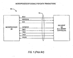
- FIG. 1 is a simplified block diagram of a conventional microprocessor interface system
- FIG. 2 is a timing diagram illustrating interaction of the signals described with reference to the conventional microprocessor interface system of FIG. 1 for performing a read transaction R1 followed by three write transactions W1, W2 and W3;
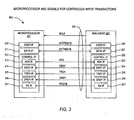
- FIG. 3 is a simplified block diagram of an exemplary microprocessor interface system implemented according to an embodiment the present invention.
- FIG. 4 is a timing diagram illustrating interaction of the signals described with reference to the microprocessor interface system of FIG. 3 for performing a read transaction R1 followed by three write transactions W1-W3 according to an exemplary embodiment of the present invention.
- the inventor of the present application has recognized that it is disadvantageous to not fully utilize the bandwidth of a processor bus of a microprocessor, whether that bus is quad pumped or otherwise. He has further noted that since processor buses typically operate at clock speeds many times slower than that of microprocessor core clocks, it is crucial to execute combined writes to memory with optimum efficiency. The inventor has recognized that inefficient utilization of bus bandwidth is a consequence of the TRP rules for deasserting TRDY, which make it difficult if not impossible to saturate the data portion of the bus with write data.
- FIG. 1 is a simplified block diagram of a conventional microprocessor interface system 100.
- the microprocessor interface system 100 includes a microprocessor 101 and a bus agent 103 interfaced with a processor bus 105.
- the bus agent 103 represents any number of different types of bus agents as known to those skilled in the art, such as a memory controller, a host/PCI (Peripheral Component Interconnect) bridge, etc.
- the processor bus 105 includes the signals for performing data transactions, including a bidirectional address bus ADDR, a bidirectional data bus DATA, and multiple control signals.
- the ADDR bus has 36 signals shown as ADDR[35:0] and the DATA bus has 64 signals shown as DATA[63:0], although it is understood that the address and data buses may have any suitable number of signals depending upon the particular configuration and architecture.
- the control signals include a bus clock signal BCLK, a bidirectional address strobe signal ADS (indicating validity of the addresses on the ADDR bus), a bidirectional data bus busy signal DBSY (asserted by the entity that is providing data on the DATA bus), a data ready signal DRDY (asserted by either the device providing data during all clock cycles that data is transferred over the DATA bus), a target ready signal TRDY (asserted only by the target device from which a write transaction has been requested), and a response bus RS which provides the type of transaction response that is being completed over the DATA bus.
- the RS bus has 3 signals shown as RS[2:0] to indicate up to 8 different transaction types.
- FIG. 2 is a timing diagram illustrating interaction of the signals described with reference to the conventional microprocessor interface system 100 for performing a read transaction R1 followed by three write transactions W1, W2 and W3.
- the BCLK, ADS, TRDY, DBSY and DRDY signals along with the RS and DATA buses are plotted versus time.
- the ADDR bus is not shown and it is noted that the address (i.e., Request A and Request B packets) is provided over the ADDR bus for respective transactions R1 and W1-W3 during assertion of the corresponding address strobe ADS.
- the microprocessor 101 provides the address and the bus agent 103 latches the address upon detection of the ADS signals.
- control signals are shown asserted as a logic low level although one skilled in the art appreciates that assertion can as well be indicated by a logic high level. Operation of such transactions and corresponding signals as named herein in an x86-compatible microprocessor are described in numerous references, including the book “Pentium Pro and Pentium II System Architecture 2nd Edition,” by Tom Shanley and U.S. Patent Application Publication 2001/0037421 AI, published November 1, 2001 and entitled “Enhanced Highly Pipelined Bus Architecture,”.
- Cycles of the BCLK clock signal are shown across the top of the timing diagram along with cycle numbers and the timing of transitions of the states of the signals are described with respect to the corresponding cycle number.
- ADS is asserted by the microprocessor 101 (along with request A/B packets provided over the ADDR bus) to request a read transaction R1 followed by the three write transactions W1-W3.
- delays are ignored and it is understood that actual signal transitions occur during the cycle immediately following the illustrated signal transition.
- the falling edge of the ADS signal to initiate the W1 write transaction shown occurring at the rising edge of the BLCK signal between clock cycles 2 and 3 actually occurs during clock cycle 3 after a relatively short delay.
- Numerous write transactions such as W1-W3 are typically executed for writes to memory of write combined buffers and the like.
- the bus agent 103 asserts DBSY, thus taking ownership of the processor bus 105.
- the bus agent asserts DRDY and transfers the read data to the microprocessor 101 over the DATA bus.
- the type of transaction is provided over the RS bus.
- the bus agent 103 deasserts DBSY allowing for other bus agents or devices to take ownership of the processor bus 105.
- the bus agent 103 asserts the TRDY signal during cycle 6 to indicate its readiness to accept write data associated with the write cycle W1 indicated by the microprocessor 101.
- the bus agent 103 deasserts the DRDY signal, thus indicating completion of the read transaction R1.
- the TRP rules include a fundamental rule that TRDY cannot be deasserted until the cycle following the cycle where the bus agent 103 confirms that DBSY has been deasserted.
- the bus agent 103 since the bus agent 103 itself is the entity that deasserts DBSY, it can deassert TRDY during the following cycle. This case is illustrated for read transaction R1. But if the microprocessor 101 (or another bus agent) is controlling the state of DBSY (as in the case of a write transaction), then the bus agent 103 must hold TRDY asserted during the cycle that it samples DBSY deasserted, which is in the cycle following deassertion of DBSY by the microprocessor 101.
- the bus agent 103 asserts TRDY to indicate its readiness for the write transaction W1 and, because the bus agent 103 is the agent that deasserts DBSY during cycle 7, it can deassert TRDY during cycle 8. But during cycles 9 and 10, the microprocessor 101 takes control of DBSY and TRDY to complete the write transaction W1. And since the microprocessor 101 deasserts DBSY in cycle 10, the bus agent 103 must wait until cycle 11 to sample DBSY deasserted, and hence cannot deassert TRDY until cycle 12. Because of this constraint, there is no way to fully utilize the bandwidth of the processor bus 105. Presently DBSY must be sampled deasserted prior to deasserting TRDY.
- a system and method according to the present invention provides an improved target readiness protocol that allows for abutted writes to memory.
- an embodiment according to the present invention decouples the relationship between DBSY and TRDY.
- TRDY is a one-cycle pulse that indicates readiness for write data, and can be asserted as early as the first clock of a previous data transfer's data phase.
- Driving of DATA is still dependent on desertion of DBSY, but deassertion is either sampled or construed.
- a bus agent providing the read data can "construe" deassertion of DBSY during the same cycle that it deasserts the signal. Thus, the bus agent does not wait until the following cycle to sample the signal that it deasserts.
- RS is provided one clock after the TRDY assertion to allow the next cycle of TRDY to be accepted, and is not provided before the last transfer of the previous data phase.
- Apparatus and method are provided in a microprocessor interface system implemented according to an embodiment of the present invention to determine and execute assertion/deassertion of TRDY and DBSY, thus allowing for writes to occur back-to-back over the processor bus.
- FIG. 3 is a simplified block diagram of an exemplary microprocessor interface system 300 implemented according to an embodiment the present invention.
- the processor bus 105 includes the same bus signals except shown in different order according to address, data and control portions.
- the bus signals operate in a substantially similar manner except for operation of TRDY relative to DBSY as further described below.
- the microprocessor 101 is replaced with a microprocessor 301 which includes an address bus interface 310, a data bus interface 311, and a control interface 312.
- the control interface 312 further includes an ADS interface 313 interfacing the ADS signals, a DBSY interface 314 interfacing the DBSY signal, a TRDY interface 315 interfacing the TRDY signal, a DRDY interface 316 interfacing the DRDY signal and an RS interface 317 interfacing the RS signals.
- the interfaces 310-312 are coupled together within the microprocessor 301 and the interfaces 313-317 are coupled together within the control interface 312 to collectively enable contiguous writes to be executed on the processor bus 105 in this quad-pumped bus architecture. It is noted that the microprocessor 101 includes similar interfaces but is implemented according to the conventional TRP rules and thus is unable to perform contiguous writes.
- the bus agent 103 is replaced with a bus agent 303 which includes an address bus interface 320, a data bus interface 321, and a control interface 322.
- the control interface 322 further includes an ADS interface 323 interfacing the ADS signals, a DBSY interface 324 interfacing the DBSY signal, a TRDY interface 325 interfacing the TRDY signal, a DRDY interface 326 interfacing the DRDY signal and an RS interface 327 interfacing the RS signals.
- the interfaces 320-322 are coupled together within the bus agent 303 and the interfaces 323-327 are coupled together within the control interface 322 to collectively enable contiguous writes to be executed on the processor bus 105 in this quad-pumped bus architecture.
- the bus agent 103 may include similar interfaces but is implemented according to the conventional TRP rules and thus is unable to perform contiguous writes.
- the ADS interface 313 asserts the ADS signals to initiate a write cycle on the processor bus 105 and the ADDR interface 310 simultaneously asserts a corresponding address on the ADDR bus.
- the TRDY interface 315 monitors the TRDY signal in response to the write cycle request.
- the RS interface 327 asserts the signals on the RS bus during the clock cycle following the clock cycle in which the TRDY signal was asserted to indicate the write cycle.
- the DRDY interface 316 asserts the DRDY signal during the clock cycle following the clock cycle in which the RS bus signals are asserted.
- the DBSY interface 314 asserts the DBSY signal for one clock cycle during the clock cycle following the clock cycle in which the RS bus signals are asserted.
- the data bus interface 311 asserts data for the write cycle on the DATA bus simultaneously with the assertion of the DRDY signals.
- the control interface 312 of the microprocessor 301 construes deassertion of the DBSY signal. In this manner, the microprocessor 301 is able to assert data on the DATA bus in the next clock cycle following deassertion of the DBSY signal without having to sample the DBSY signal deasserted on the DATA bus.
- the ADS interface 323 detects the request for the write cycle via the assertion of the ADS signals.
- the data busy interface 324 detects assertion of the DBSY signal during a data phase of a prior data transfer cycle.
- the TRDY interface 325 asserts the TRDY signal in response to the write cycle request for one clock cycle during a first clock cycle of a data phase of a prior write cycle or during a second clock cycle of a prior read cycle. The additional clock delay for the read cycle allows for switch-back on the processor bus 105 between read and write cycles.
- the TRDY signal may be asserted as early as the first clock of the previous data transfer's data phase, the TRDY may be asserted simultaneously with the DBSY signal for all of the contiguous write cycles except the first write cycle if the previous data transfer is a read cycle. If the previous data transfer is a read cycle, then the TRDY signal is asserted during the second clock of the prior read cycle's data phase.
- the RS interface 317 detects assertion of the signals on the RS bus indicating the data transfer phase of the write cycle.
- the DRDY interface 326 detects assertion of the DRDY signal indicating that data is valid on the DATA bus.
- the DATA bus interface 321 retrieves the data in response to the DRDY signal being asserted.
- FIG. 4 is a timing diagram illustrating interaction of the signals described with reference to the microprocessor interface system 300 for performing a read transaction R1 followed by three write transactions W1-W3 according to an exemplary embodiment of the present invention.
- the BCLK, ADS, TRDY, DBSY and DRDY signals along with the RS and DATA buses are plotted versus time.
- the ADDR bus is not shown and it is noted that the address (i.e., Request A and Request B packets) for the respective transactions R1 and W1-W3 are provided during assertion of the address strobe ADS.
- the microprocessor 301 provides the address and the bus agent 303 latches the address upon detection of the ADS signals.
- the control signals are shown asserted as a logic low level although one skilled in the art appreciates that assertion can as well be indicated by a logic high level.
- cycles of the bus clock BCLK are shown across the top of the timing diagram.
- the ADS signal is asserted (along with request A/B packets provided over the ADDR bus) by the ADS interface 313 to request a read transaction R1 followed by three write transactions W1-W3 in the same manner.
- the DBSY interface 324 of the bus agent 103 asserts DBSY, thus taking ownership of the processor bus 105 for the read cycle R1.
- the DRDY interface 326 of the bus agent 303 asserts DRDY and the DATA bus interface 321 transfers the read data to the microprocessor 301 over the DATA bus.
- the type of transaction is provided over the RS bus by the RS interface 327.
- the TRDY signal is a one-cycle pulse that indicates readiness for write data, and can be asserted as early as the first clock of a previous data transfer's data phase or as early as the second clock of the data phase of a previous read cycle in the illustrated embodiment.
- the TRDY interface 325 of the bus agent 303 asserts TRDY during cycle 7 because, since it is the entity deasserting DBSY during cycle 7, deassertion of DBSY is construed during the same cycle. Because TRDY assertion is one cycle according to an embodiment of the present invention, TRDY is deasserted during cycle 8. Also during cycle 8, DRDY is deasserted, thus indicating completion of the read transaction R1.
- the protocol according to an embodiment of the present invention allows for deassertion of TRDY immediately in the next clock cycle after it has been asserted. Accordingly, a following write transaction is allowed to begin in the clock cycle following deassertion of TRDY and to support this new feature, the type of transaction is provided over the RS bus during the same cycle that TRDY is deasserted, that is, one cycle after TRDY assertion.
- the TRDY interface 325 of the bus agent 303 asserts TRDY to indicate readiness for W1 in cycle 7.
- the response for W1 over the RS bus begins in cycle 8 and the data for W1 is transferred during cycles 9 and 10 between the DATA bus interfaces 311 and 321.
- deassertion of DBSY and TRDY during cycle 12 allows for transfer of the W3 data during cycles 13 and 14 (not shown).
- the microprocessor 301 construes deassertion of the DBSY signal in cycle 12 to enable early data transfer in next cycle 13.
- three abutted writes W1-W3 are executed during cycles 9-14, thus fully saturating the processor bus 105.
- Decoupling the relationship between TRDY and DBSY thus allows the processor bus 105 to be fully saturated with write data, which is a 33% improvement over the conventional microprocessor interface system 100 operating according to the conventional TRP rules.
- the present invention has been described in considerable detail with reference to certain preferred versions thereof, other versions and variations are possible and contemplated.
- the present invention also contemplates other mechanisms to allow for full speed write transactions over the bus.
- One such mechanism employs two TRDY signals. With two TRDY signals, target readiness could be indicated by either of the two TRDY signals being asserted. This would eliminate the delay incurred upon deassertion of a single TRDY signal.
- those skilled in the art should appreciate that they can readily use the disclosed conception and specific embodiments as a basis for designing or modifying other structures for carrying out the same purposes of the present invention.
Landscapes
- Engineering & Computer Science (AREA)
- Theoretical Computer Science (AREA)
- Physics & Mathematics (AREA)
- General Engineering & Computer Science (AREA)
- General Physics & Mathematics (AREA)
- Information Transfer Systems (AREA)
- Bus Control (AREA)
Claims (13)
- Verfahren zum Ausführen zusammenhängender Schreibtransaktionen zwischen einem Prozessor (301) und einem Busagenten (303) auf einem Prozessorbus (105), gekennzeichnet durch die Schritte:durch den Busagenten (303) das Erfassen einer Anforderung für einen Schreibzyklus;durch den Busagenten (303) das Setzen eines Ziel-Bereit-Signals für einen Taktzyklus als Reaktion auf den Schreibzyklus während eines ersten Taktzyklus einer Datenübertragungsphase eines vorhergehenden Schreibzyklus, wobei das Ziel-Bereit-Signal ein Impuls ist, der einen Zyklus andauert;durch den Busagenten (303) das Setzen von Antwortsignalen in einem nächsten Taktzyklus, der auf den Taktzyklus folgt, in dem das Ziel-Bereit-Signal gesetzt wird;durch den Prozessor (301) das Setzen eines Daten-Belegt-Signals für den Schreibzyklus in dem nächsten Taktzyklus, der auf den Taktzyklus folgt, in dem die Antwortsignale gesetzt werden; unddurch den Prozessor (301) das Anlegen von Daten für den Schreibzyklus wenn das Daten-Belegt-Signal gesetzt ist.
- Verfahren nach Anspruch 1, zudem umfassend:durch den Busagenten (303) das Erfassen einer Anforderung für jeden Zyklus einer Anzahl zusammenhängender Schreibzyklen;durch den Busagenten (303) das Setzen des Ziel-Bereit-Signals für einen Taktzyklus als Reaktion auf jeden zusammenhängenden Schreibzyklus während eines ersten Taktzyklus einer Datenübertragungsphase eines vorhergehenden zusammenhängenden Schreibzyklus;durch den Busagenten (303) das Setzen von Antwortsignalen für jeden zusammenhängenden Schreibzyklus in einem nächsten Taktzyklus, der auf den Taktzyklus folgt, in dem das Ziel-Bereit-Signal gesetzt wird;durch den Prozessor das Setzen des Daten-Belegt-Signals für jeden zusammenhängenden Schreibzyklus in dem nächsten Taktzyklus, der auf den Taktzyklus folgt, in dem die Antwortsignale gesetzt werden; unddurch den Prozessor das Anlegen von Daten für jeden zusammenhängenden Schreibzyklus wenn das Daten-Belegt-Signal gesetzt ist.
- Verfahren nach Anspruch 1, wobei das Erfassen einer Anforderung für einen Schreibzyklus das Zwischenspeichern einer Adresse umfasst, die einen Ort zum Speichern der Daten angibt.
- Verfahren nach Anspruch 1, wobei das Setzen des Ziel-Bereit-Signals für den Schreibzyklus während eines ersten Taktzyklus einer Datenübertragungsphase eines vorhergehenden Schreibzyklus das gleichzeitige Setzen des Ziel-Bereit-Signals und des Daten-Belegt-Signals umfasst.
- Verfahren nach Anspruch 1, zudem umfassend durch den Prozessor (301) das Ausbilden des Zurücksetzens des Daten-Belegt-Signals, nachdem es für den Schreibzyklus gesetzt ist.
- Verfahren nach Anspruch 1, wobei das Setzen von Antwortsignalen das Setzen von Antwortsignalen umfasst, die einen Typ der Transaktionsantwort für den Schreibzyklus anzeigen.
- Verfahren nach Anspruch 1, wobei das Anlegen von Daten für den Schreibzyklus das Anlegen von Daten an einen Datenabschnitt des Prozessorbusses umfasst.
- Verfahren nach Anspruch 7, zudem umfassend das Setzen eines Daten-Bereit-Signals gleichzeitig mit dem Anlegen der Daten für den Schreibzyklus.
- Prozessor (301), gekennzeichnet durch:eine Steuerbus-Schnittstelle (312; 322), die: eine Anforderung für einen Schreibzyklus anlegt; das Setzen eines Ziel-Bereit-Signals für den Schreibzyklus erkennt; das Setzen von Antwortsignalen einen Taktzyklus nach dem Setzen des Ziel-Bereit-Signals erkennt; und die ein Daten-Belegt-Signal einen Taktzyklus nach dem Setzen der Antwortsignale setzt;eine Datenbus-Schnittstelle (311; 321), die mit der Steuerbus-Schnittstelle gekoppelt ist und Daten für den Schreibzyklus liefert, wenn das Daten-Belegt-Signal gesetzt wird; undeine Adressbus-Schnittstelle (310; 320), die eine Adresse liefert, wenn die Anforderung für den Schreibzyklus angelegt wird, wobei:die Steuerbus-Schnittstelle eine Ziel-Bereit-Schnittstelle (315) umfasst, die das Ziel-Bereit-Signal für den Schreibzyklus während eines ersten Taktzyklus einer Datenübertragungsphase eines vorhergehenden Schreibzyklus erkennt; unddas Ziel-Bereit-Signal einen Impuls umfasst, der einen Zyklus andauert.
- Prozessor nach Anspruch 9, wobei die Steuerbus-Schnittstelle eine Adressimpuls-Schnittstelle umfasst, die die Anforderung für einen Schreibzyklus liefert.
- Prozessor nach Anspruch 9, wobei die Steuerbus-Schnittstelle eine Daten-Belegt-Schnittstelle umfasst, die das Wegnehmen des Daten-Belegt-Signals während des Schreibzyklus ausbildet.
- Prozessor nach Anspruch 9, wobei die Steuerbus-Schnittstelle eine Antwortschnittstelle umfasst, die das Anlegen der Antwortsignale nach dem Setzen des Ziel-Bereit-Signals erfasst.
- Prozessor nach Anspruch 9, wobei die Steuerbus-Schnittstelle zudem eine Daten-Bereit-Schnittstelle umfasst, die Daten-Bereit-Signale anlegt, die angeben, dass die Daten für den Schreibzyklus angelegt sind.
Applications Claiming Priority (2)
| Application Number | Priority Date | Filing Date | Title |
|---|---|---|---|
| US69706305P | 2005-07-05 | 2005-07-05 | |
| US11/358,464 US7543094B2 (en) | 2005-07-05 | 2006-02-21 | Target readiness protocol for contiguous write |
Publications (3)
| Publication Number | Publication Date |
|---|---|
| EP1760601A2 EP1760601A2 (de) | 2007-03-07 |
| EP1760601A3 EP1760601A3 (de) | 2009-09-16 |
| EP1760601B1 true EP1760601B1 (de) | 2011-07-06 |
Family
ID=37619538
Family Applications (1)
| Application Number | Title | Priority Date | Filing Date |
|---|---|---|---|
| EP06251163A Active EP1760601B1 (de) | 2005-07-05 | 2006-03-03 | Zielfertigkeitsprotokoll für kontinuierliches Schreiben |
Country Status (4)
| Country | Link |
|---|---|
| US (1) | US7543094B2 (de) |
| EP (1) | EP1760601B1 (de) |
| CN (1) | CN100403286C (de) |
| TW (1) | TWI325539B (de) |
Families Citing this family (3)
| Publication number | Priority date | Publication date | Assignee | Title |
|---|---|---|---|---|
| US9263106B2 (en) * | 2011-10-21 | 2016-02-16 | Nvidia Corporation | Efficient command mapping scheme for short data burst length memory devices |
| WO2014176775A1 (zh) | 2013-05-02 | 2014-11-06 | 华为技术有限公司 | 一种计算机系统、高速外围组件互联端点设备的访问方法、和装置 |
| CN105938461B (zh) * | 2015-07-31 | 2019-02-19 | 杭州迪普科技股份有限公司 | 一种dma数据传输方法、装置以及网络设备 |
Family Cites Families (6)
| Publication number | Priority date | Publication date | Assignee | Title |
|---|---|---|---|---|
| US5237670A (en) * | 1989-01-30 | 1993-08-17 | Alantec, Inc. | Method and apparatus for data transfer between source and destination modules |
| US5426739A (en) * | 1992-03-16 | 1995-06-20 | Opti, Inc. | Local bus - I/O Bus Computer Architecture |
| US5790811A (en) * | 1996-05-17 | 1998-08-04 | Advanced Micro Devices, Inc. | System and method for performing data transfers during PCI idle clock cycles |
| US6336159B1 (en) * | 1997-06-25 | 2002-01-01 | Intel Corporation | Method and apparatus for transferring data in source-synchronous protocol and transferring signals in common clock protocol in multiple agent processing system |
| US6311245B1 (en) * | 1998-06-05 | 2001-10-30 | Micron Technology, Inc. | Method for time multiplexing a low-speed and a high-speed bus over shared signal lines of a physical bus |
| US6609171B1 (en) * | 1999-12-29 | 2003-08-19 | Intel Corporation | Quad pumped bus architecture and protocol |
-
2006
- 2006-02-21 US US11/358,464 patent/US7543094B2/en active Active
- 2006-03-03 EP EP06251163A patent/EP1760601B1/de active Active
- 2006-07-05 TW TW095124437A patent/TWI325539B/zh active
- 2006-07-05 CN CNB2006101013536A patent/CN100403286C/zh active Active
Also Published As
| Publication number | Publication date |
|---|---|
| CN1881193A (zh) | 2006-12-20 |
| EP1760601A2 (de) | 2007-03-07 |
| US20070011376A1 (en) | 2007-01-11 |
| TWI325539B (en) | 2010-06-01 |
| CN100403286C (zh) | 2008-07-16 |
| US7543094B2 (en) | 2009-06-02 |
| EP1760601A3 (de) | 2009-09-16 |
| TW200703013A (en) | 2007-01-16 |
Similar Documents
| Publication | Publication Date | Title |
|---|---|---|
| USRE37980E1 (en) | Bus-to-bus bridge in computer system, with fast burst memory range | |
| US6085274A (en) | Computer system with bridges having posted memory write buffers | |
| US6321286B1 (en) | Fault tolerant computer system | |
| US5870567A (en) | Delayed transaction protocol for computer system bus | |
| US5440751A (en) | Burst data transfer to single cycle data transfer conversion and strobe signal conversion | |
| US5935233A (en) | Computer system with a switch interconnector for computer devices | |
| US6098134A (en) | Lock protocol for PCI bus using an additional "superlock" signal on the system bus | |
| US6266719B1 (en) | High-throughput interface between a system memory controller and a peripheral device | |
| EP1909187B1 (de) | Verfahren und Vorrichtung zur Unterstützung verzögerter Transaktionen multifunktionaler PCI-Geräte in PCI-Brücken | |
| US5918072A (en) | System for controlling variable length PCI burst data using a dummy final data phase and adjusting the burst length during transaction | |
| US6209053B1 (en) | Method and apparatus for operating an adaptive multiplexed address and data bus within a computer system | |
| WO1994008303A1 (en) | Method and apparatus for non-snoop window reduction | |
| US7171509B2 (en) | Method and apparatus for host messaging unit for Peripheral Component Interconnect busmaster devices | |
| US6631437B1 (en) | Method and apparatus for promoting memory read commands | |
| USRE40921E1 (en) | Mechanism for efficiently processing deferred order-dependent memory access transactions in a pipelined system | |
| US5559968A (en) | Non-conforming PCI bus master timing compensation circuit | |
| US5964856A (en) | Mechanism for data strobe pre-driving during master changeover on a parallel bus | |
| US7054987B1 (en) | Apparatus, system, and method for avoiding data writes that stall transactions in a bus interface | |
| US5832243A (en) | Computer system implementing a stop clock acknowledge special cycle | |
| US6789153B1 (en) | Bridge for coupling digital signal processor to on-chip bus as slave | |
| US5590316A (en) | Clock doubler and smooth transfer circuit | |
| EP1760601B1 (de) | Zielfertigkeitsprotokoll für kontinuierliches Schreiben | |
| US5754825A (en) | Lower address line prediction and substitution | |
| US6041380A (en) | Method for increasing the number of devices capable of being operably connected to a host bus | |
| US7779188B2 (en) | System and method to reduce memory latency in microprocessor systems connected with a bus |
Legal Events
| Date | Code | Title | Description |
|---|---|---|---|
| PUAI | Public reference made under article 153(3) epc to a published international application that has entered the european phase |
Free format text: ORIGINAL CODE: 0009012 |
|
| AK | Designated contracting states |
Kind code of ref document: A2 Designated state(s): AT BE BG CH CY CZ DE DK EE ES FI FR GB GR HU IE IS IT LI LT LU LV MC NL PL PT RO SE SI SK TR |
|
| AX | Request for extension of the european patent |
Extension state: AL BA HR MK YU |
|
| PUAL | Search report despatched |
Free format text: ORIGINAL CODE: 0009013 |
|
| AK | Designated contracting states |
Kind code of ref document: A3 Designated state(s): AT BE BG CH CY CZ DE DK EE ES FI FR GB GR HU IE IS IT LI LT LU LV MC NL PL PT RO SE SI SK TR |
|
| AX | Request for extension of the european patent |
Extension state: AL BA HR MK YU |
|
| 17P | Request for examination filed |
Effective date: 20091027 |
|
| 17Q | First examination report despatched |
Effective date: 20091119 |
|
| AKX | Designation fees paid |
Designated state(s): DE ES FR GB |
|
| GRAP | Despatch of communication of intention to grant a patent |
Free format text: ORIGINAL CODE: EPIDOSNIGR1 |
|
| GRAS | Grant fee paid |
Free format text: ORIGINAL CODE: EPIDOSNIGR3 |
|
| GRAA | (expected) grant |
Free format text: ORIGINAL CODE: 0009210 |
|
| AK | Designated contracting states |
Kind code of ref document: B1 Designated state(s): DE ES FR GB |
|
| REG | Reference to a national code |
Ref country code: GB Ref legal event code: FG4D |
|
| REG | Reference to a national code |
Ref country code: DE Ref legal event code: R096 Ref document number: 602006022895 Country of ref document: DE Effective date: 20110901 |
|
| REG | Reference to a national code |
Ref country code: ES Ref legal event code: FG2A Ref document number: 2368938 Country of ref document: ES Kind code of ref document: T3 Effective date: 20111123 |
|
| PLBE | No opposition filed within time limit |
Free format text: ORIGINAL CODE: 0009261 |
|
| STAA | Information on the status of an ep patent application or granted ep patent |
Free format text: STATUS: NO OPPOSITION FILED WITHIN TIME LIMIT |
|
| 26N | No opposition filed |
Effective date: 20120411 |
|
| REG | Reference to a national code |
Ref country code: DE Ref legal event code: R097 Ref document number: 602006022895 Country of ref document: DE Effective date: 20120411 |
|
| REG | Reference to a national code |
Ref country code: FR Ref legal event code: PLFP Year of fee payment: 11 |
|
| REG | Reference to a national code |
Ref country code: FR Ref legal event code: PLFP Year of fee payment: 12 |
|
| REG | Reference to a national code |
Ref country code: FR Ref legal event code: PLFP Year of fee payment: 13 |
|
| REG | Reference to a national code |
Ref country code: DE Ref legal event code: R082 Ref document number: 602006022895 Country of ref document: DE Representative=s name: HL KEMPNER PATENTANWAELTE, SOLICITORS (ENGLAND, DE Ref country code: DE Ref legal event code: R082 Ref document number: 602006022895 Country of ref document: DE Representative=s name: HL KEMPNER PATENTANWALT, RECHTSANWALT, SOLICIT, DE Ref country code: DE Ref legal event code: R082 Ref document number: 602006022895 Country of ref document: DE Representative=s name: HL KEMPNER PARTG MBB, DE |
|
| PGFP | Annual fee paid to national office [announced via postgrant information from national office to epo] |
Ref country code: DE Payment date: 20250331 Year of fee payment: 20 |
|
| PGFP | Annual fee paid to national office [announced via postgrant information from national office to epo] |
Ref country code: FR Payment date: 20250224 Year of fee payment: 20 |
|
| PGFP | Annual fee paid to national office [announced via postgrant information from national office to epo] |
Ref country code: GB Payment date: 20250224 Year of fee payment: 20 |
|
| PGFP | Annual fee paid to national office [announced via postgrant information from national office to epo] |
Ref country code: ES Payment date: 20250403 Year of fee payment: 20 |