EP1758437A2 - Laminated structure including a resin layer containing a glass-cloth and method for manufacturing the same - Google Patents
Laminated structure including a resin layer containing a glass-cloth and method for manufacturing the same Download PDFInfo
- Publication number
- EP1758437A2 EP1758437A2 EP06017441A EP06017441A EP1758437A2 EP 1758437 A2 EP1758437 A2 EP 1758437A2 EP 06017441 A EP06017441 A EP 06017441A EP 06017441 A EP06017441 A EP 06017441A EP 1758437 A2 EP1758437 A2 EP 1758437A2
- Authority
- EP
- European Patent Office
- Prior art keywords
- resin layer
- layer
- glass
- insulating
- cloth containing
- Prior art date
- Legal status (The legal status is an assumption and is not a legal conclusion. Google has not performed a legal analysis and makes no representation as to the accuracy of the status listed.)
- Withdrawn
Links
- 229920005989 resin Polymers 0.000 title claims abstract description 93
- 239000011347 resin Substances 0.000 title claims abstract description 93
- 239000004744 fabric Substances 0.000 title claims abstract description 53
- 238000000034 method Methods 0.000 title claims description 23
- 238000004519 manufacturing process Methods 0.000 title claims description 13
- 238000010030 laminating Methods 0.000 claims description 2
- 239000010410 layer Substances 0.000 description 138
- 239000011799 hole material Substances 0.000 description 53
- 239000002365 multiple layer Substances 0.000 description 18
- 239000000463 material Substances 0.000 description 9
- 230000002787 reinforcement Effects 0.000 description 5
- 230000015572 biosynthetic process Effects 0.000 description 4
- 239000000945 filler Substances 0.000 description 3
- 239000011521 glass Substances 0.000 description 3
- 239000002245 particle Substances 0.000 description 3
- 239000000758 substrate Substances 0.000 description 3
- 230000000694 effects Effects 0.000 description 2
- 239000002131 composite material Substances 0.000 description 1
- 239000004020 conductor Substances 0.000 description 1
- 238000007796 conventional method Methods 0.000 description 1
- 230000001419 dependent effect Effects 0.000 description 1
- 239000003822 epoxy resin Substances 0.000 description 1
- 238000009413 insulation Methods 0.000 description 1
- 239000011229 interlayer Substances 0.000 description 1
- 239000007769 metal material Substances 0.000 description 1
- 238000007747 plating Methods 0.000 description 1
- 229920000647 polyepoxide Polymers 0.000 description 1
- 239000000126 substance Substances 0.000 description 1
- 208000016261 weight loss Diseases 0.000 description 1
- 239000013585 weight reducing agent Substances 0.000 description 1
Images

Classifications
-
- B—PERFORMING OPERATIONS; TRANSPORTING
- B32—LAYERED PRODUCTS
- B32B—LAYERED PRODUCTS, i.e. PRODUCTS BUILT-UP OF STRATA OF FLAT OR NON-FLAT, e.g. CELLULAR OR HONEYCOMB, FORM
- B32B3/00—Layered products comprising a layer with external or internal discontinuities or unevennesses, or a layer of non-planar shape; Layered products comprising a layer having particular features of form
- B32B3/26—Layered products comprising a layer with external or internal discontinuities or unevennesses, or a layer of non-planar shape; Layered products comprising a layer having particular features of form characterised by a particular shape of the outline of the cross-section of a continuous layer; characterised by a layer with cavities or internal voids ; characterised by an apertured layer
-
- B—PERFORMING OPERATIONS; TRANSPORTING
- B32—LAYERED PRODUCTS
- B32B—LAYERED PRODUCTS, i.e. PRODUCTS BUILT-UP OF STRATA OF FLAT OR NON-FLAT, e.g. CELLULAR OR HONEYCOMB, FORM
- B32B17/00—Layered products essentially comprising sheet glass, or glass, slag, or like fibres
- B32B17/06—Layered products essentially comprising sheet glass, or glass, slag, or like fibres comprising glass as the main or only constituent of a layer, next to another layer of a specific material
- B32B17/10—Layered products essentially comprising sheet glass, or glass, slag, or like fibres comprising glass as the main or only constituent of a layer, next to another layer of a specific material of synthetic resin
-
- H—ELECTRICITY
- H05—ELECTRIC TECHNIQUES NOT OTHERWISE PROVIDED FOR
- H05K—PRINTED CIRCUITS; CASINGS OR CONSTRUCTIONAL DETAILS OF ELECTRIC APPARATUS; MANUFACTURE OF ASSEMBLAGES OF ELECTRICAL COMPONENTS
- H05K1/00—Printed circuits
- H05K1/02—Details
- H05K1/03—Use of materials for the substrate
- H05K1/0313—Organic insulating material
- H05K1/0353—Organic insulating material consisting of two or more materials, e.g. two or more polymers, polymer + filler, + reinforcement
- H05K1/0366—Organic insulating material consisting of two or more materials, e.g. two or more polymers, polymer + filler, + reinforcement reinforced, e.g. by fibres, fabrics
-
- H—ELECTRICITY
- H05—ELECTRIC TECHNIQUES NOT OTHERWISE PROVIDED FOR
- H05K—PRINTED CIRCUITS; CASINGS OR CONSTRUCTIONAL DETAILS OF ELECTRIC APPARATUS; MANUFACTURE OF ASSEMBLAGES OF ELECTRICAL COMPONENTS
- H05K3/00—Apparatus or processes for manufacturing printed circuits
- H05K3/0011—Working of insulating substrates or insulating layers
- H05K3/0017—Etching of the substrate by chemical or physical means
- H05K3/0026—Etching of the substrate by chemical or physical means by laser ablation
- H05K3/0032—Etching of the substrate by chemical or physical means by laser ablation of organic insulating material
-
- H—ELECTRICITY
- H05—ELECTRIC TECHNIQUES NOT OTHERWISE PROVIDED FOR
- H05K—PRINTED CIRCUITS; CASINGS OR CONSTRUCTIONAL DETAILS OF ELECTRIC APPARATUS; MANUFACTURE OF ASSEMBLAGES OF ELECTRICAL COMPONENTS
- H05K3/00—Apparatus or processes for manufacturing printed circuits
- H05K3/0011—Working of insulating substrates or insulating layers
- H05K3/0017—Etching of the substrate by chemical or physical means
- H05K3/0026—Etching of the substrate by chemical or physical means by laser ablation
- H05K3/0032—Etching of the substrate by chemical or physical means by laser ablation of organic insulating material
- H05K3/0035—Etching of the substrate by chemical or physical means by laser ablation of organic insulating material of blind holes, i.e. having a metal layer at the bottom
-
- H—ELECTRICITY
- H05—ELECTRIC TECHNIQUES NOT OTHERWISE PROVIDED FOR
- H05K—PRINTED CIRCUITS; CASINGS OR CONSTRUCTIONAL DETAILS OF ELECTRIC APPARATUS; MANUFACTURE OF ASSEMBLAGES OF ELECTRICAL COMPONENTS
- H05K3/00—Apparatus or processes for manufacturing printed circuits
- H05K3/46—Manufacturing multilayer circuits
- H05K3/4644—Manufacturing multilayer circuits by building the multilayer layer by layer, i.e. build-up multilayer circuits
-
- H—ELECTRICITY
- H05—ELECTRIC TECHNIQUES NOT OTHERWISE PROVIDED FOR
- H05K—PRINTED CIRCUITS; CASINGS OR CONSTRUCTIONAL DETAILS OF ELECTRIC APPARATUS; MANUFACTURE OF ASSEMBLAGES OF ELECTRICAL COMPONENTS
- H05K3/00—Apparatus or processes for manufacturing printed circuits
- H05K3/46—Manufacturing multilayer circuits
- H05K3/4644—Manufacturing multilayer circuits by building the multilayer layer by layer, i.e. build-up multilayer circuits
- H05K3/4673—Application methods or materials of intermediate insulating layers not specially adapted to any one of the previous methods of adding a circuit layer
-
- H—ELECTRICITY
- H05—ELECTRIC TECHNIQUES NOT OTHERWISE PROVIDED FOR
- H05K—PRINTED CIRCUITS; CASINGS OR CONSTRUCTIONAL DETAILS OF ELECTRIC APPARATUS; MANUFACTURE OF ASSEMBLAGES OF ELECTRICAL COMPONENTS
- H05K2201/00—Indexing scheme relating to printed circuits covered by H05K1/00
- H05K2201/01—Dielectrics
- H05K2201/0183—Dielectric layers
- H05K2201/0195—Dielectric or adhesive layers comprising a plurality of layers, e.g. in a multilayer structure
Definitions
- This invention relates to a laminated product, in particular to a laminated product in a structure including a glass-cloth containing resin layer, and to a method for manufacturing the same. More specifically, this invention relates to a product in a multiple-layer structure including a layer of glass-cloth containing resin known as "prepreg" as a reinforcement layer, e.g. a product such as a multiple-layer substrate or package, and a method for manufacturing the same.
- a "build-up" technique As a method for manufacturing a multiple-layer structure such as a multiple-layer wiring board, a "build-up" technique is known.
- the build-up technique on a core substrate with a wiring layer formed as a first layer, insulating layers and wiring layers are alternately formed, or formed one on the other, to form a wiring board in a multiple-layer structure.
- a via hole passing through the insulating layers between these wiring layers is made.
- the product in a multiple-layer structure has been manufactured by inserting a prepreg layer giving a high reinforcement effect. This is attributable to the fact that although the prepreg is known as a material inferior in laser processing, owing to improvements of a laser processing technique, also in the multiple-layer structure including a prepreg layer for reinforcement, the via hole for conduction between the layers has become capable of being formed.
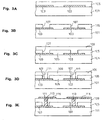
- FIG. 3A A technique for making the via hole in fabrication of the wiring board in the multiple-layer structure including the prepreg is disclosed in JP-A-2004-356232 (henceforth referred to as Patent Reference 1).
- Fig. 3B After a prepreg insulating layer 105 overlying a lower wiring layer 103 formed on a substrate 101 has been formed, as shown in Fig. 3B, a large-diameter hole 107 from which a part of the lower wiring layer 103 is exposed is made thereon by laser processing.
- Fig. 3C an insulating resin layer 109 overlying the prepreg insulating layer 105 is formed. Further, as shown in Fig.
- a small-diameter hole 111 is made by laser processing. Thereafter, as shown in Fig. 3E, the small-diameter hole 111 is subjected to conducting processing to form a via hole 113. After the via hole 113 has been formed, an upper wiring layer 115 connected to the via hole 113 can be formed.
- the laser processing must be done twice in the formation of the via hole 113 for making the larger-diameter hole 107 and small-diameter hole 111, thereby complicating the processing steps.
- higher laser processing accuracy is required than the case of making a single hole.
- subjecting the small-diameter hole 111 which is preferably 120 to 50 ⁇ m to the conducting processing cannot be carried out so easily.
- the present invention intends to reduce at least some of the above problems.
- the object is solved by the laminated product according to independent claim 1, and by method for manufacturing a laminated product according to independent claim 5.
- a laminated product including: a wiring layer and an insulating layer being alternately laminated, i.e. laminated one on the other, and different wiring layers being electrically connected to each other by a via hole passing through the insulating layer, wherein at least one of the insulating layers is a laminated body including: an insulating resin layer on a lower wiring layer and a glass-cloth containing resin layer thereon, and in the laminated body, the via hole continuously passes through from the glass-cloth containing resin layer to the insulating resin layer.
- the laminated product is provided in a structure including a glass-cloth containing resin layer.
- the at least one insulating layer is formed of the laminated body.
- the via hole passes through from the upper glass-cloth containing layer to the lower insulating resin layer.
- a laminated product comprising wiring layers and one or more insulating layers, the wiring layers and the one or more insulating layers being laminated one on the other, wherein different ones of the wiring layers are electrically connected to each other by a via hole passing through the one or more insulating layers, and wherein at least one of the one or more insulating layers is a laminated body including: an insulating resin layer on a lower wiring layer and a glass-cloth containing resin layer thereon, and wherein in the laminated body, the via hole continuously passes through from the glass-cloth containing resin layer to the insulating resin layer.
- a laminated product including a glass-cloth containing resin layer is manufactured by a method including the steps of: laminating at least one, preferably more than one, set of a wiring layer and an insulating layer, one on the other, on a lower board with a wiring layer, and electrically connecting different ones of the wiring layers to each other by a via hole passing through the insulating layer or layers, making at least one of the insulating layer or layers be a laminated body including: an insulating resin layer and a glass-cloth containing resin layer successively formed on a lower wiring layer, and laser processing the laminated body so that a hole for making the via hole is continuously made from the glass-cloth containing resin layer to the insulating resin layer.
- a conventional method for making the via hole which requires that different resin layers are formed and laser processing is done for the resin layers, respectively, high laser processing accuracy is required as compared with the collective laser processing for two layers.
- the laminated product according to this invention capable of collectively laser-processing the glass-cloth containing resin layer and the insulating resin layer therebelow can be given as a multiple-layer product by a simple step and at low cost.
- conduction processing for the thorough-hole can be done more simply as compared with the conduction processing for the hole with a small diameter which is finally made by executing the laser processing twice according to the conventional art.
- a laminated product including a glass-cloth containing resin layer having a multiple-layer structure capable of making a via hole by a simple step, and a method for manufacturing the same can be achieved.
- the invention is also directed to apparatuses for carrying out the disclosed methods and including apparatus parts for performing each described method steps. These method steps may be performed by way of hardware components, a computer programmed by appropriate software, by any combination of the two or in any other manner.
- Fig. 1 schematically shows a laminated product 1 in a structure including a glass-cloth containing resin layer, i. e. a resin layer containing a glass-cloth, according to this invention.
- the laminated product 1 as shown in Fig. 1 includes an insulating resin layer 7 overlying a lower wiring board 3 equipped with a lower wiring layer 5, and a glass-cloth containing resin layer 9, the insulating resin layer 7 and the glass-cloth containing resin layer 9 constituting a single insulating layer 11.
- an upper wiring layer 13 is located on the insulating layer 11.
- the lower wiring layer 5 and the upper wiring layer 13 are electrically connected by a via hole 17 of a conductive material filled into a hole 15 which successively passes through the glass-cloth containing resin layer 9 and insulating resin layer 7.
- the "hole continuously passing through” means that the hole for the via hole passing from upper glass-cloth containing resin to the lower insulating resin layer extends from the glass-cloth containing resin layer to the insulating resin layer without substantially discontinuously changing the diameter at the interface or its vicinity between the glass-cloth containing resin layer and the insulating resin layer, i.e. without forming a level difference due to a change in the diameter at the interface and its vicinity between both layers.
- On the upper wire layer 13, another set of the insulating layer and wiring layer may exist.
- the lower wiring board 3 equipped with the lower wiring layer 5 may be a core board which is used to manufacture a multiple-layer board having a build-up layer formed thereon. Otherwise, it may be such a core board having at least one set of an insulating layer and a wiring layer built-up thereon.
- the insulating resin layer 7 which constitutes the insulating layer 11 can be made of an insulating resin which is generally used to form an interlayer insulating layer in the multiple-layer wiring board.
- This insulating resin may contain e.g. a filler of glass particles.
- the glass-cloth containing resin layer 9 located on the insulating resin layer 7 is made by impregnating the glass-cloth with the insulating resin, and is made of the material called "prepreg". Both materials can be selected from the materials which are generally used in manufacture of the multiple-layer wiring board.
- the glass-cloth containing resin material used to form the glass-cloth containing resin layer 9 is commercially available as a product having a predetermined thickness.
- the product having a sufficient thickness to obtain a necessary reinforcement effect can be selectively adapted.
- the material having the thickness of about 40 ⁇ m or 60 ⁇ m can be employed.
- the insulating resin layer 7 underlying the glass-cloth resin layer 9 is formed with such a thickness that the laminated body of itself and the glass-cloth containing resin layer 9 has the thickness necessary to assure the insulation between the upper and lower wiring layers.
- the thickness is generally about 40 to 100 ⁇ m.
- the via hole 17 which continuously passes through the upper glass-cloth containing resin layer 9 and the lower insulating resin layer 7 can be formed by a CO 2 laser device as in a common via hole material.
- the diameter of the via hole 17 is not particularly limited, but generally 100 to 300 ⁇ m, preferably about 150 to 200 ⁇ m.
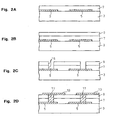
- FIGs. 2A to 2D an explanation will be given of manufacture of the laminated product in a structure including a glass-cloth containing resin layer according to this invention.
- the insulating resin layer 7 (thickness of 40 ⁇ m) covering the lower wiring layer 5 overlying the lower wiring board 3 is formed.
- This insulating resin layer 7 can be formed of epoxy resin containing e.g. a glass particle filler by about 20 wt %.
- a glass-cloth containing resin sheet is placed on the insulating resin layer 7 and stamped to form the glass-cloth containing resin layer 9 as shown in Fig. 2B.
- the glass-cloth containing resin sheet may be GHPL-830HS (thickness of 40 ⁇ m) which is commercially available from e.g. Mitsubishi Gas Chemical Company, Inc.
- the glass-cloth containing resin layer 9 and the insulating resin layer 7 underlying it are successively processed to make a hole 15 having a diameter of 150 ⁇ m which passes through the glass-cloth containing resin layer 9 and the insulating resin layer 7 so as to expose a part of the lower wiring layer 5, as shown in Fig. 2C.
- the lower wiring layer 5 (or possibly a pad communicating with the lower wiring layer 5) made of the metallic material of e.g. Cu exposed to the bottom of the hole 15 by the processing serves as a stopper so that the processing can be completed when the depth of the hole 15 reaches the lower wiring layer 5.
- the glass-cloth containing resin layer 9 is inferior to the insulating resin layer 7 having the filler of glass particles.
- the laser processing capability can be defined by the speed of formation of a via hole by a laser, i.e. a superior or inferior laser processing capability implies a fast or slow formation of a via hole by a laser, respectively.
- the hole 15 is filled with Cu plating by the ordinary technique to form a via hole 17.
- the upper wiring layer 13 can also be formed by a known technique.
- another set (not shown) of the insulating layer and wiring layer can be formed.
- the laminated product according to this invention has been explained with reference to the multiple-layer board.
- the laminated product according to this invention can also be applied to various products in a multiple-layer structure including the glass-cloth containing resin layer as a reinforcement layer, e.g. a package product. Therefore, it should be understood that the laminated product according to this invention includes these various products.
Landscapes
- Engineering & Computer Science (AREA)
- Microelectronics & Electronic Packaging (AREA)
- Manufacturing & Machinery (AREA)
- Physics & Mathematics (AREA)
- Optics & Photonics (AREA)
- Production Of Multi-Layered Print Wiring Board (AREA)
- Laminated Bodies (AREA)
Abstract
Description
- This invention relates to a laminated product, in particular to a laminated product in a structure including a glass-cloth containing resin layer, and to a method for manufacturing the same. More specifically, this invention relates to a product in a multiple-layer structure including a layer of glass-cloth containing resin known as "prepreg" as a reinforcement layer, e.g. a product such as a multiple-layer substrate or package, and a method for manufacturing the same.
- As a method for manufacturing a multiple-layer structure such as a multiple-layer wiring board, a "build-up" technique is known. In the build-up technique, on a core substrate with a wiring layer formed as a first layer, insulating layers and wiring layers are alternately formed, or formed one on the other, to form a wiring board in a multiple-layer structure. For conduction between different wiring layers, a via hole passing through the insulating layers between these wiring layers is made.
- In order to satisfy the demand of downsizing or weight-reduction in recent years for electronic components, low-profiling of the multiple-layer wiring board is required. In order to realize this, in recent years, the product in a multiple-layer structure has been manufactured by inserting a prepreg layer giving a high reinforcement effect. This is attributable to the fact that although the prepreg is known as a material inferior in laser processing, owing to improvements of a laser processing technique, also in the multiple-layer structure including a prepreg layer for reinforcement, the via hole for conduction between the layers has become capable of being formed.
- A technique for making the via hole in fabrication of the wiring board in the multiple-layer structure including the prepreg is disclosed in
JP-A-2004-356232 prepreg insulating layer 105 overlying alower wiring layer 103 formed on asubstrate 101 has been formed, as shown in Fig. 3B, a large-diameter hole 107 from which a part of thelower wiring layer 103 is exposed is made thereon by laser processing. Next, as shown in Fig. 3C, aninsulating resin layer 109 overlying the prepreg insulatinglayer 105 is formed. Further, as shown in Fig. 3D, inside the large-diameter hole 107, a small-diameter hole 111 is made by laser processing. Thereafter, as shown in Fig. 3E, the small-diameter hole 111 is subjected to conducting processing to form avia hole 113. After thevia hole 113 has been formed, anupper wiring layer 115 connected to thevia hole 113 can be formed. - In the method for manufacturing the multiple-layer wiring board disclosed in Patent Reference 1, the laser processing must be done twice in the formation of the
via hole 113 for making the larger-diameter hole 107 and small-diameter hole 111, thereby complicating the processing steps. In addition, in order to make the small-diameter hole inside the large-diameter hole, higher laser processing accuracy is required than the case of making a single hole. Further, subjecting the small-diameter hole 111 which is preferably 120 to 50 µm to the conducting processing cannot be carried out so easily. - The present invention intends to reduce at least some of the above problems. The object is solved by the laminated product according to independent claim 1, and by method for manufacturing a laminated product according to
independent claim 5. - Further advantages, features, aspects and details of the invention are evident from the dependent claims, the description and the drawings.
- According to the present invention, there is provided a laminated product including: a wiring layer and an insulating layer being alternately laminated, i.e. laminated one on the other, and different wiring layers being electrically connected to each other by a via hole passing through the insulating layer, wherein at least one of the insulating layers is a laminated body including: an insulating resin layer on a lower wiring layer and a glass-cloth containing resin layer thereon, and in the laminated body, the via hole continuously passes through from the glass-cloth containing resin layer to the insulating resin layer.
- Preferably, the laminated product is provided in a structure including a glass-cloth containing resin layer. Preferably, the at least one insulating layer is formed of the laminated body. Preferably, the via hole passes through from the upper glass-cloth containing layer to the lower insulating resin layer.
- Further, there is provided, according to the invention, a laminated product comprising wiring layers and one or more insulating layers, the wiring layers and the one or more insulating layers being laminated one on the other, wherein different ones of the wiring layers are electrically connected to each other by a via hole passing through the one or more insulating layers, and wherein at least one of the one or more insulating layers is a laminated body including: an insulating resin layer on a lower wiring layer and a glass-cloth containing resin layer thereon, and wherein in the laminated body, the via hole continuously passes through from the glass-cloth containing resin layer to the insulating resin layer.
- Further, a laminated product including a glass-cloth containing resin layer according to the present invention is manufactured by a method including the steps of: laminating at least one, preferably more than one, set of a wiring layer and an insulating layer, one on the other, on a lower board with a wiring layer, and electrically connecting different ones of the wiring layers to each other by a via hole passing through the insulating layer or layers, making at least one of the insulating layer or layers be a laminated body including: an insulating resin layer and a glass-cloth containing resin layer successively formed on a lower wiring layer, and laser processing the laminated body so that a hole for making the via hole is continuously made from the glass-cloth containing resin layer to the insulating resin layer.
- In accordance with this invention, there is provided a via hole made using a continuous through-hole made by collectively laser-processing a glass-cloth containing resin layer and an insulating resin layer therebelow which constitute a composite insulating layer lying between an upper and a lower wiring layer. In the case of a conventional method for making the via hole which requires that different resin layers are formed and laser processing is done for the resin layers, respectively, high laser processing accuracy is required as compared with the collective laser processing for two layers. On the other hand, the laminated product according to this invention capable of collectively laser-processing the glass-cloth containing resin layer and the insulating resin layer therebelow can be given as a multiple-layer product by a simple step and at low cost. Further, in accordance with this invention, conduction processing for the thorough-hole can be done more simply as compared with the conduction processing for the hole with a small diameter which is finally made by executing the laser processing twice according to the conventional art.
- Thus, a laminated product including a glass-cloth containing resin layer having a multiple-layer structure capable of making a via hole by a simple step, and a method for manufacturing the same can be achieved.
- The invention is also directed to apparatuses for carrying out the disclosed methods and including apparatus parts for performing each described method steps. These method steps may be performed by way of hardware components, a computer programmed by appropriate software, by any combination of the two or in any other manner.
- The invention will be better understood by reference to the following description of embodiments of the invention taken in conjunction with the accompanying drawings, wherein:
- Fig. 1 is a schematic view for explaining the laminated product in a structure including a glass-cloth containing resin layer according to this invention.
- Figs. 2A to 2D are views for explaining manufacture of a multiple-layer product according to this invention.
- Figs. 3A to 3E are views for explaining formation of a via hole in the laminated product in a structure including a glass-cloth containing resin layer according to a conventional art.
- Fig. 1 schematically shows a laminated product 1 in a structure including a glass-cloth containing resin layer, i. e. a resin layer containing a glass-cloth, according to this invention. The laminated product 1 as shown in Fig. 1 includes an
insulating resin layer 7 overlying alower wiring board 3 equipped with alower wiring layer 5, and a glass-cloth containingresin layer 9, theinsulating resin layer 7 and the glass-cloth containingresin layer 9 constituting a single insulating layer 11. On the insulating layer 11, anupper wiring layer 13 is located. Thelower wiring layer 5 and theupper wiring layer 13 are electrically connected by avia hole 17 of a conductive material filled into ahole 15 which successively passes through the glass-cloth containingresin layer 9 and insulatingresin layer 7. In this invention, the "hole continuously passing through" means that the hole for the via hole passing from upper glass-cloth containing resin to the lower insulating resin layer extends from the glass-cloth containing resin layer to the insulating resin layer without substantially discontinuously changing the diameter at the interface or its vicinity between the glass-cloth containing resin layer and the insulating resin layer, i.e. without forming a level difference due to a change in the diameter at the interface and its vicinity between both layers. On theupper wire layer 13, another set of the insulating layer and wiring layer may exist. - The
lower wiring board 3 equipped with thelower wiring layer 5 may be a core board which is used to manufacture a multiple-layer board having a build-up layer formed thereon. Otherwise, it may be such a core board having at least one set of an insulating layer and a wiring layer built-up thereon. - The
insulating resin layer 7 which constitutes the insulating layer 11 can be made of an insulating resin which is generally used to form an interlayer insulating layer in the multiple-layer wiring board. This insulating resin may contain e.g. a filler of glass particles. The glass-cloth containingresin layer 9 located on theinsulating resin layer 7 is made by impregnating the glass-cloth with the insulating resin, and is made of the material called "prepreg". Both materials can be selected from the materials which are generally used in manufacture of the multiple-layer wiring board. - The glass-cloth containing resin material used to form the glass-cloth containing
resin layer 9 is commercially available as a product having a predetermined thickness. The product having a sufficient thickness to obtain a necessary reinforcement effect can be selectively adapted. For example, the material having the thickness of about 40 µm or 60 µm can be employed. Theinsulating resin layer 7 underlying the glass-cloth resin layer 9 is formed with such a thickness that the laminated body of itself and the glass-cloth containingresin layer 9 has the thickness necessary to assure the insulation between the upper and lower wiring layers. The thickness is generally about 40 to 100 µm. - The
via hole 17 which continuously passes through the upper glass-cloth containingresin layer 9 and the lowerinsulating resin layer 7 can be formed by a CO2 laser device as in a common via hole material. The diameter of thevia hole 17 is not particularly limited, but generally 100 to 300 µm, preferably about 150 to 200 µm. - Now referring to Figs. 2A to 2D, an explanation will be given of manufacture of the laminated product in a structure including a glass-cloth containing resin layer according to this invention.
- As shown in Fig. 2A, the insulating resin layer 7 (thickness of 40 µm) covering the
lower wiring layer 5 overlying thelower wiring board 3 is formed. This insulatingresin layer 7 can be formed of epoxy resin containing e.g. a glass particle filler by about 20 wt %. A glass-cloth containing resin sheet is placed on the insulatingresin layer 7 and stamped to form the glass-cloth containingresin layer 9 as shown in Fig. 2B. The glass-cloth containing resin sheet may be GHPL-830HS (thickness of 40 µm) which is commercially available from e.g. Mitsubishi Gas Chemical Company, Inc. - Subsequently, using the laser device LC-2G manufactured by e.g. Hitachi Via Mechanics, Ltd, the glass-cloth containing
resin layer 9 and the insulatingresin layer 7 underlying it are successively processed to make ahole 15 having a diameter of 150 µm which passes through the glass-cloth containingresin layer 9 and the insulatingresin layer 7 so as to expose a part of thelower wiring layer 5, as shown in Fig. 2C. During the laser processing, the lower wiring layer 5 (or possibly a pad communicating with the lower wiring layer 5) made of the metallic material of e.g. Cu exposed to the bottom of thehole 15 by the processing serves as a stopper so that the processing can be completed when the depth of thehole 15 reaches thelower wiring layer 5. As regards laser processing capability, the glass-cloth containingresin layer 9 is inferior to the insulatingresin layer 7 having the filler of glass particles. The laser processing capability can be defined by the speed of formation of a via hole by a laser, i.e. a superior or inferior laser processing capability implies a fast or slow formation of a via hole by a laser, respectively. - Generally, where the processing of hole making is successively executed for different materials, if the processing is executed precedently for the material having good laser processing capability and subsequently for the material poor laser processing capability, at the stage when the processing is shifted from the former to the latter, an inconvenience such as reduction of a processing diameter occurs. On the other hand, if the processing is executed precedently for the glass-cloth containing
resin layer 9 having poor laser processing capability and subsequently for the insulatingresin layer 7 having good laser processing capability, without being plagued with the inconvenience such as reduction in the processing diameter, a hole having substantially the same diameter as that made in the glass-cloth containingresin layer 9 can be made in the lower insulatingresin layer 7. In addition, the collective processing of hole making for the upper glass-cloth containingresin layer 9 and lower insulatingresin layer 7 will not face the inevitable problem of strict laser processing accuracy in the method disclosed in Patent Reference 1 in which after the hole having a large diameter has been made, another hole having a diameter smaller than the large diameter is made within the hole having the large diameter. - Next, as shown in Fig. 2D, the
hole 15 is filled with Cu plating by the ordinary technique to form a viahole 17. Thereafter, theupper wiring layer 13 can also be formed by a known technique. On theupper wire layer 13, another set (not shown) of the insulating layer and wiring layer can be formed. - Hitherto, the laminated product according to this invention has been explained with reference to the multiple-layer board. However, without being limited to it, the laminated product according to this invention can also be applied to various products in a multiple-layer structure including the glass-cloth containing resin layer as a reinforcement layer, e.g. a package product. Therefore, it should be understood that the laminated product according to this invention includes these various products.
Claims (8)
- A laminated product comprising:a wiring layer (5, 13) and an insulating layer (11) being laminated one on the other, anddifferent wiring layers (5, 13) being electrically connected to each other by a via hole (17) passing through the insulating layer (11), whereinat least one of the insulating layers (11) is a laminated body including: an insulating resin layer (7) on a lower wiring layer (5) and a glass-cloth containing resin layer (9) thereon, andin the laminated body, the via hole (17) continuously passes through from the glass-cloth containing resin layer (9) to the insulating resin layer (7).
- The laminated product according to claim 1, wherein
the glass-cloth containing resin layer (9) is inferior to the insulating resin layer (7) as regards laser processing capability. - The laminated product according to any of the claims 1 or 2, wherein
the diameter of the via hole (17) is 100 to 300 µm. - The laminated product according to any of the claims 1 to 3, wherein
the diameter of the via hole (17) is about 150 to 200 µm. - A method for manufacturing a laminated product including a glass-cloth containing resin layer (9) comprising the steps of:laminating at least one set of a wiring layer (5, 13) and an insulating layer (11), one on the other, on a lower board with a wiring layer (5), andelectrically connecting different wiring layers (5, 13) to each other by a via hole (15) passing through the insulating layer (11),making at least one of insulating layers (11) be a laminated body including: an insulating resin layer (7) and a glass-cloth containing resin layer (9) successively formed on a lower wiring layer (5), andlaser processing the laminated body so that a hole (15) for making the via hole (17) is continuously made from the glass-cloth containing resin layer (9) to the insulating resin layer (7).
- The method according to claim 5, wherein
the diameter of the via hole (17) is 100 to 300 µm. - The method according to claim 5 or 6, wherein
the diameter of the via hole (17) is about 150 to 200 µm. - The method according to any of claims 5 to 7, wherein
the glass-cloth containing resin layer (9) is inferior to the insulating resin layer (7) as regards laser processing capability.
Applications Claiming Priority (1)
| Application Number | Priority Date | Filing Date | Title |
|---|---|---|---|
| JP2005244219A JP2007059689A (en) | 2005-08-25 | 2005-08-25 | Laminated product having a structure including a glass cloth-containing resin layer and a method for producing the same |
Publications (2)
| Publication Number | Publication Date |
|---|---|
| EP1758437A2 true EP1758437A2 (en) | 2007-02-28 |
| EP1758437A3 EP1758437A3 (en) | 2007-07-25 |
Family
ID=37606848
Family Applications (1)
| Application Number | Title | Priority Date | Filing Date |
|---|---|---|---|
| EP06017441A Withdrawn EP1758437A3 (en) | 2005-08-25 | 2006-08-22 | Laminated structure including a resin layer containing a glass-cloth and method for manufacturing the same |
Country Status (6)
| Country | Link |
|---|---|
| US (1) | US20070045811A1 (en) |
| EP (1) | EP1758437A3 (en) |
| JP (1) | JP2007059689A (en) |
| KR (1) | KR20070024373A (en) |
| CN (1) | CN1921732A (en) |
| TW (1) | TW200723991A (en) |
Families Citing this family (5)
| Publication number | Priority date | Publication date | Assignee | Title |
|---|---|---|---|---|
| TWI611922B (en) * | 2008-03-25 | 2018-01-21 | Ajinomoto Co., Inc. | Insulating resin sheet and method of manufacturing multilayer printed circuit board using the same |
| JP2010034197A (en) * | 2008-07-28 | 2010-02-12 | Fujitsu Ltd | Buildup board |
| KR101056898B1 (en) * | 2008-09-11 | 2011-08-12 | 주식회사 두산 | Multilayer printed circuit board and its manufacturing method |
| TWI471073B (en) | 2009-12-31 | 2015-01-21 | Unimicron Technology Corp | Circuit substrate and manufacturing method thereof |
| US9941219B2 (en) | 2014-09-19 | 2018-04-10 | Intel Corporation | Control of warpage using ABF GC cavity for embedded die package |
Citations (1)
| Publication number | Priority date | Publication date | Assignee | Title |
|---|---|---|---|---|
| JP2004356232A (en) | 2003-05-27 | 2004-12-16 | Matsushita Electric Works Ltd | Method for manufacturing multilayer printed wiring board |
Family Cites Families (8)
| Publication number | Priority date | Publication date | Assignee | Title |
|---|---|---|---|---|
| JPH09199858A (en) * | 1996-01-19 | 1997-07-31 | Shinko Electric Ind Co Ltd | Method for manufacturing multilayer wiring board |
| US6320140B1 (en) * | 1996-06-14 | 2001-11-20 | Ibiden Co., Ltd. | One-sided circuit board for multi-layer printed wiring board, multi-layer printed wiring board, and method of its production |
| US6284308B2 (en) * | 1998-12-25 | 2001-09-04 | Victor Company Of Japan, Ltd. | Manufacturing method of printed circuit board |
| JP2000255001A (en) * | 1999-03-05 | 2000-09-19 | Ibiden Co Ltd | Laminated substrate and insulating layer thereof |
| US6423905B1 (en) * | 2000-05-01 | 2002-07-23 | International Business Machines Corporation | Printed wiring board with improved plated through hole fatigue life |
| US6459046B1 (en) * | 2000-08-28 | 2002-10-01 | Matsushita Electric Industrial Co., Ltd. | Printed circuit board and method for producing the same |
| EP1194020A3 (en) * | 2000-09-27 | 2004-03-31 | Matsushita Electric Industrial Co., Ltd. | Resin board, manufacturing process for resin board, connection medium body, circuit board and manufacturing process for circuit board |
| JP4055474B2 (en) * | 2002-05-28 | 2008-03-05 | 株式会社トッパンNecサーキットソリューションズ | Multilayer circuit board manufacturing method |
-
2005
- 2005-08-25 JP JP2005244219A patent/JP2007059689A/en active Pending
-
2006
- 2006-08-08 US US11/463,166 patent/US20070045811A1/en not_active Abandoned
- 2006-08-15 TW TW095129910A patent/TW200723991A/en unknown
- 2006-08-22 EP EP06017441A patent/EP1758437A3/en not_active Withdrawn
- 2006-08-22 KR KR1020060079174A patent/KR20070024373A/en not_active Withdrawn
- 2006-08-25 CN CNA2006101099787A patent/CN1921732A/en active Pending
Patent Citations (1)
| Publication number | Priority date | Publication date | Assignee | Title |
|---|---|---|---|---|
| JP2004356232A (en) | 2003-05-27 | 2004-12-16 | Matsushita Electric Works Ltd | Method for manufacturing multilayer printed wiring board |
Also Published As
| Publication number | Publication date |
|---|---|
| EP1758437A3 (en) | 2007-07-25 |
| KR20070024373A (en) | 2007-03-02 |
| TW200723991A (en) | 2007-06-16 |
| CN1921732A (en) | 2007-02-28 |
| JP2007059689A (en) | 2007-03-08 |
| US20070045811A1 (en) | 2007-03-01 |
Similar Documents
| Publication | Publication Date | Title |
|---|---|---|
| EP1659841B1 (en) | Printed circuit board | |
| US9307651B2 (en) | Fabricating process of embedded circuit structure | |
| TW201206287A (en) | Printed wiring board and method for manufacturing printed wiring board | |
| US9107313B2 (en) | Method of manufacturing a hybrid heat-radiating substrate | |
| US6637105B1 (en) | Method of manufacturing a multilayer printed wiring board | |
| US20020170827A1 (en) | Multilayer substrate for a buildup with a via, and method for producing the same | |
| CN1332598A (en) | Printed-wiring board with cavity for mounting electronic component and manufacture thereof | |
| US20160330836A1 (en) | Printed wiring board | |
| KR101332079B1 (en) | Method of manufacturing a multi-layer printed circuit board and a multi-layer printed circuit board manufactured by the same | |
| CN100435602C (en) | Method for manufacturing electronic component and electronic component | |
| US20140166355A1 (en) | Method of manufacturing printed circuit board | |
| JP4792749B2 (en) | Manufacturing method of printed wiring board with built-in electronic components | |
| JP2006190928A (en) | BGA package and manufacturing method thereof | |
| CN108463065B (en) | Substrate and method for manufacturing the same | |
| WO2020213624A1 (en) | Via substrate, electronic unit, method for manufacture of via substrate, and method for manufacture of electronic unit | |
| KR102141681B1 (en) | Manufacturing method of multilayer substrate | |
| US20070045811A1 (en) | Laminated product in structure including glass-cloth contained resin layer and method for manufacturing the same | |
| JP2010123829A (en) | Printed wiring board and manufacturing method thereof | |
| JP3684830B2 (en) | Printed wiring board | |
| KR20110028330A (en) | Wiring board and its manufacturing method | |
| KR101034089B1 (en) | Wiring board and its manufacturing method | |
| CN1980540A (en) | Circuit board structure and its manufacturing method | |
| US7926172B2 (en) | Embedded circuit board and process thereof | |
| JP2002374068A (en) | Method for manufacturing multilayered printed circuit board | |
| JPH08264940A (en) | Through hole processing method for printed wiring board |
Legal Events
| Date | Code | Title | Description |
|---|---|---|---|
| PUAI | Public reference made under article 153(3) epc to a published international application that has entered the european phase |
Free format text: ORIGINAL CODE: 0009012 |
|
| AK | Designated contracting states |
Kind code of ref document: A2 Designated state(s): AT BE BG CH CY CZ DE DK EE ES FI FR GB GR HU IE IS IT LI LT LU LV MC NL PL PT RO SE SI SK TR |
|
| AX | Request for extension of the european patent |
Extension state: AL BA HR MK YU |
|
| PUAL | Search report despatched |
Free format text: ORIGINAL CODE: 0009013 |
|
| AK | Designated contracting states |
Kind code of ref document: A3 Designated state(s): AT BE BG CH CY CZ DE DK EE ES FI FR GB GR HU IE IS IT LI LT LU LV MC NL PL PT RO SE SI SK TR |
|
| AX | Request for extension of the european patent |
Extension state: AL BA HR MK YU |
|
| AKX | Designation fees paid | ||
| STAA | Information on the status of an ep patent application or granted ep patent |
Free format text: STATUS: THE APPLICATION IS DEEMED TO BE WITHDRAWN |
|
| 18D | Application deemed to be withdrawn |
Effective date: 20080126 |
|
| REG | Reference to a national code |
Ref country code: DE Ref legal event code: 8566 |