EP1758167A2 - Phase change memory array having equalized resistance - Google Patents
Phase change memory array having equalized resistance Download PDFInfo
- Publication number
- EP1758167A2 EP1758167A2 EP06016871A EP06016871A EP1758167A2 EP 1758167 A2 EP1758167 A2 EP 1758167A2 EP 06016871 A EP06016871 A EP 06016871A EP 06016871 A EP06016871 A EP 06016871A EP 1758167 A2 EP1758167 A2 EP 1758167A2
- Authority
- EP
- European Patent Office
- Prior art keywords
- phase
- memory cells
- line
- change memory
- change
- Prior art date
- Legal status (The legal status is an assumption and is not a legal conclusion. Google has not performed a legal analysis and makes no representation as to the accuracy of the status listed.)
- Granted
Links
Images









Classifications
-
- G—PHYSICS
- G11—INFORMATION STORAGE
- G11C—STATIC STORES
- G11C13/00—Digital stores characterised by the use of storage elements not covered by groups G11C11/00, G11C23/00, or G11C25/00
- G11C13/0002—Digital stores characterised by the use of storage elements not covered by groups G11C11/00, G11C23/00, or G11C25/00 using resistive RAM [RRAM] elements
- G11C13/0004—Digital stores characterised by the use of storage elements not covered by groups G11C11/00, G11C23/00, or G11C25/00 using resistive RAM [RRAM] elements comprising amorphous/crystalline phase transition cells
-
- H—ELECTRICITY
- H10—SEMICONDUCTOR DEVICES; ELECTRIC SOLID-STATE DEVICES NOT OTHERWISE PROVIDED FOR
- H10B—ELECTRONIC MEMORY DEVICES
- H10B63/00—Resistance change memory devices, e.g. resistive RAM [ReRAM] devices
- H10B63/80—Arrangements comprising multiple bistable or multi-stable switching components of the same type on a plane parallel to the substrate, e.g. cross-point arrays
-
- G—PHYSICS
- G11—INFORMATION STORAGE
- G11C—STATIC STORES
- G11C2213/00—Indexing scheme relating to G11C13/00 for features not covered by this group
- G11C2213/70—Resistive array aspects
- G11C2213/79—Array wherein the access device being a transistor
Definitions
- Phase-change materials exhibit at least two different states.
- the states of phase-change material may be referenced to as amorphous and crystalline states.
- the states may be distinguished because the amorphous state generally exhibits higher resistivity than does the crystalline state.
- the amorphous state involves a more disordered atomic structure, while the crystalline state is an ordered lattice.
- Some phase-change materials exhibit two crystalline states, e.g. a face-centered cubic (FCC) state and a hexagonal closest packing (HCP) state. These two crystalline states have different resistivities.
- FCC face-centered cubic
- HCP hexagonal closest packing
- Phase change in the phase-change materials may be induced reversibly.
- the phase-change material may change from the amorphous state to the crystalline state, and from the crystalline state to the amorphous state, in response to temperature changes.
- the temperature changes to the phase-change material may be achieved in a variety of ways.
- a laser can be directed to the phase-change material, current may be driven through the phase-change material, or current can be fed through a resistive heater adjacent the phase-change material.
- controllable heating of the phase-change material causes controllable phase change within the phase-change material.
- An array of phase-change memory cells includes bit line and ground line wiring. Since the bit line and ground line wiring have a parasitic resistance, the set and reset current fed through a phase-change memory cell during the application of a voltage write pulse depends on the location of the phase-change memory cell in the memory array. This location dependent set and reset current contributes to a broadening of the phase-change memory cell resistance distribution and thereby affects the reliability of the phase-change memory cell set and reset operations. Typical solutions to this problem attempt to minimize the resistance or adjust the set and reset current based on the location of the phase-change memory cell within the memory array to compensate for the voltage drop over the bit line. These methods increase the costs of the phase-change memory due to increased process complexity and chip complexity.
- One embodiment of the present invention provides a memory.
- the memory includes memory cells, a first line coupled to the memory cells, and a second line coupled to the memory cells. A series resistance of the first line plus the second line at each one of the memory cells is substantially equal.
- FIG. 1 is a diagram illustrating one embodiment of a memory 100.
- Memory 100 include a plurality of phase-change memory cells 104a-104d (collectively referred to as phase-change memory cells 104), a plurality of first lines 112a-112b (collectively referred to as first lines 112), a plurality of select lines 110a-110b (collectively referred to as select lines 110), and a plurality of second lines 114a-114b (collectively referred to as second lines 114).
- Each phase-change memory cell 104 is electrically coupled to a select line 110, a first line 112, and a second line 114. While phase-change memory cells 104 are used in the illustrated embodiment, in other embodiments, other suitable types of memory cells can be used.
- first lines 112 are referred to as bit lines 112
- second lines 114 are referred to as ground lines 114
- select lines 110 are referred to as word lines 110 due to the use of phase-change element 106 and field-effect transistor (FET) 108 within phase-change memory cell 104.
- phase-change memory cell 104c is electrically coupled to bit line (BL) 112b, word line (WL1) 110a, and ground line (GL) 114b
- phase-change memory cell 104d is electrically coupled to bit line 112b, word line (WL2) 110b, and ground line 114b.
- phase-change memory cell 104 of phase-change memory cell array 100 does not depend on the location of the phase-change memory cell in memory array 100.
- Memory array 100 balances the unavoidable, position dependent voltage drop over bit lines 112 by a voltage drop over ground lines 114, which has the inverse location dependence such that the total series resistance due to the wiring is constant for each phase-change memory cell 104 in memory array 100.
- the total series resistance for each phase-change memory cell 104 is made equal by the parallel routing of bit lines 112 and ground lines 114 and the connection of bit lines 112 and ground lines 114 at opposite sides 102 and 103 of memory array 100, respectively, so that the total wiring length in memory array 100 is the same for each phase-change memory cell 104.
- each bit line 112 and each ground line 114 has the same resistance per length (resistance/length).
- the same resistance/length can be achieved by a reduction in thickness of the higher metallization line (e.g., Al, Cu) which typically has a lower resistivity than lower metallization levels (e.g., W).
- bit lines 112 and ground lines 114 in memory array 100 run in parallel and the line resistance of bit lines 112 and the line resistance of ground lines 114 are approximately equal so that the actual write voltage of an individual phase-change memory cell 104 is not dependent on the position of phase-change memory cell 104 in memory array 100.
- memory array 100 includes two memory cells 104a and 104b.
- bit line 112a and ground line 114a run in parallel and the line resistance of bit line 112a and the line resistance of ground line 114a are approximately equal.
- one or more of the bit lines 112 have an orientation to one or more of the ground lines 114 that is not parallel.
- each phase-change memory cell 104 includes a phase-change element 106 and a transistor 108. While transistor 108 is a FET in the illustrated embodiment, in other embodiments, transistor 108 can be other suitable devices such as a bipolar transistor or a 3D transistor structure.
- phase-change memory cell 104c includes phase-change element 106a and transistor 108a. One side of phase-change element 106a is electrically coupled to bit line 112b and the other side of phase-change element 106a is electrically coupled to one side of the source-drain path of transistor 108a. The other side of the source-drain path of transistor 108a is electrically coupled to ground line 114b.
- phase-change memory cell 104d includes phase-change element 106b and transistor 108b.
- One side of phase-change element 106b is electrically coupled to bit line 112b and the other side of phase-change element 106b is electrically coupled to one side of the source-drain path of transistor 108b.
- the other side of the source-drain path of transistor 108b is electrically coupled to ground line 114b.
- the gate of transistor 108b is electrically coupled to word line 110b.
- each phase-change element 106 comprises a phase-change material that may be made up of a variety of suitable materials in accordance with the present invention.
- suitable materials such as GeSbTe, SbTe, or AgInSbTe.
- the phase-change material can be chalcogen free, such as GeSb, GaSb, or GeGaSb.
- bit lines 112 are connected to additional circuits on one side 102 of memory array 100, and ground lines 114 are connected to additional circuits on another side 103 of memory array 100.
- Side 102 of memory array 100 is opposite side 103 of memory array 100.
- bit lines 112 are parallel to ground lines 114.
- bit lines 112 can have other suitable orientations to ground lines 114.
- the length of bit line 112b from phase-change memory cell 104c to side 102 of memory array 100 is indicated at 118, and the length of bit line 112b from phase-change memory cell 104d to side 102 of memory array 100 is indicated at 116.
- the length of ground line 114b from phase-change memory cell 104c to side 103 of memory array 100 is indicated at 120, and the length of ground line 114b from phase-change memory cell 104d to side 103 of memory array 100 is indicated at 122.
- bit line 112b and ground line 114b have the same resistance/length so that the series resistance due to bit line 112b and ground line 114b are equal for both phase-change memory cells 104c and 104d.
- different resistance and lengths can be used for bit line 112b and ground line 114b such that the series resistance due to bit line 112b and ground line 114b are equal for both phase-change memory cells 104c and 104d.
- the series resistance due to bit lines 112 and ground lines 114 for each phase-change memory cell 104 in memory array 100 is substantially equal. Therefore, the write current and/or voltage for setting or resetting a phase-change memory cell 104 is the same for all phase-change memory cells 104 in memory array 100. While four memory cells 104 are illustrated in Figure 1, in other embodiments, two memory cells 104 are used and are coupled to the same bit line 112 and ground line 114.
- phase-change element 106a reaches its crystalline state during this set operation.
- a reset current and/or voltage pulse is selectively enabled to bit line 112b and sent to phase-change material element 106a. The reset current or voltage quickly heats phase-change element 106a above its melting temperature.
- phase-change element 106a After the current and/or voltage pulse is turned off, the phase-change element 106a quickly quench cools into the amorphous state. Phase-change memory cell 104d and other phase-change memory cells 104 in array 100 are set and reset similarly to phase-change memory cell 104c using the same current and/or voltage pulse value.
- FIG. 2A illustrates a top view
- Figure 2B illustrates a side view of one embodiment of a layout 124a for dual gate phase-change memory cells.
- Dual gate phase-change memory cells include two transistors 108 that are both shared and support one phase-change element 106.
- Layout 124a includes substrate 136, bit line 112, ground line 114, shallow trench isolation (STI) 126, word lines 110, transistors 108, contacts 130, contacts 132, and phase-change elements 106.
- Bit line 112 and ground line 114 are in separate metallization layers.
- bit line 112 comprises W or another suitable metal and is in a lower metallization layer than ground line 114, which comprises Al, Cu, or another suitable metal.
- bit line 112 comprises Al, Cu, or another suitable metal and is in a higher metallization layer than ground line 114, which comprises W or another suitable metal.
- bit line 112 and ground line 114 have substantially the same resistance/length.
- Bit line 112 is spaced apart from ground line 114 by a width as indicated at 128a. In one embodiment, bit line 112 is parallel to ground line 114.
- One side of the source-drain path of each transistor 108 is electrically coupled to ground line 114 through a contact 132, which comprises Cu, W, or another suitable conductive material.
- the other side of the source-drain path of each transistor 108 is electrically coupled to a bit line 112 through a phase-change element 106 and contact 130, which comprises Cu, W, or another suitable electrically conductive material.
- the gate of each transistor 108 is electrically coupled to a word line 110, which comprises doped poly-Si, W, TiN, or another suitable material.
- phase-change elements 106 are located between transistor 108 and bit line 112.
- memory element 106 is a heater cell, an active-in-via cell, a pillar cell, or other suitable phase-change memory element.
- width 128a can be reduced to approximately zero to reduce the phase-change memory cell 104 size and therefore increase the density of the array of phase-change memory cells 100.
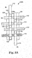
- Figure 3A illustrates a top view
- Figure 3B illustrates a side view of another embodiment of a layout 124b for dual gate phase-change memory cells.
- Layout 124b is similar to layout 124a except that in layout 124b bit line 112 and ground line 114 are in the same metallization layer and the width 128b of the space between bit line 112 and ground line 114 is greater than width 128a (Fig. 2A). Since bit line 112 and ground line 114 are in the same metallization layer, width 128b is greater than width 128a to provide adequate isolation between bit line 112 and ground line 114.
- bit line 112 and ground line 114 By locating bit line 112 and ground line 114 in the same metallization layer, the resistance/length of bit line 112 and ground line 114 is easier to equalize than if bit line 112 and ground line 114 are in separate metallization layers. To equalize the resistance/length of bit line 112 and ground line 114 in the same metallization layer, the thickness of bit line 112 is made substantially equal to the thickness of ground line 114.
- Figure 4A illustrates a top view
- Figure 4B illustrates a side view of another embodiment of a layout 124c for dual gate phase-change memory cells.
- Layout 124c is similar to layout 124a except that in layout 124c phase-change element 106 is between a transistor 108 and ground line 114 instead of between a transistor 108 and a bit line 112.
- Bit line 112 and ground line 114 are in separate metallization layers.
- bit line 112 is in a higher metallization layer than ground line 114.
- bit line 112 is in a lower metallization layer than ground line 114.
- Bit line 112 is parallel to ground line 114 and spaced apart from ground line 114 by a width as indicated at 128a.
- each transistor 108 One side of the source-drain path of each transistor 108 is electrically coupled to ground line 114 through a phase-change element 106 and contact 130. The other side of the source-drain path of each transistor 108 is electrically coupled to a bit line 112 through contact 132. The gate of each transistor 108 is electrically coupled to a word line 110.
- phase-change element 106 By fabricating phase-change element 106 after one or more of the metallization layers are deposited, the temperature budget available for processing these one or more metallization layers is improved. The improved temperature budget provides more options in selecting materials and processing methods. By locating bit line 112 and ground line 114 in separate metallization layers, width 128a can be reduced to approximately zero to reduce the phase-change memory cell 104 size and therefore increase the density of the array of phase-change memory cells 100.
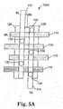
- Figure 5A illustrates a top view
- Figure 5B illustrates a side view of another embodiment of a layout 124d for dual gate phase-change memory cells.
- Layout 124d is similar to layout 124c except that in layout 124d bit line 112 and ground line 114 are in the same metallization layer and the width 128b of the space between bit line 112 and ground line 114 is greater than width 128a (Fig. 4A). Since bit line 112 and ground line 114 are in the same metallization layer, width 128b is greater than width 128a to provide adequate isolation between bit line 112 and ground line 114.
- bit line 112 and ground line 114 By locating bit line 112 and ground line 114 in the same metallization layer, the resistance/length of bit line 112 and ground line 114 is easier to equalize than if bit line 112 and ground line 114 are in separate metallization layers. To equalize the resistance/length of bit line 112 and ground line 114 in the same metallization layer, the thickness of bit line 112 is made substantially equal to the thickness of ground line 114.
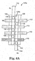
- Figure 6A illustrates a top view
- Figure 6B illustrates a side view of one embodiment of a layout 125a for single gate phase-change memory cells.
- Single gate phase-change memory cells include one transistor 108 to support one phase-change element 106.
- Layout 125a includes substrate 136, bit line 112, ground line 114, shallow trench isolation (STI) 126, word lines 110, transistors 108, contacts 130, contacts 132, and phase-change elements 106.
- Bit line 112 and ground line 114 are in separate metallization layers. In one embodiment, bit line 112 is in a higher metallization layer than ground line 114. In another embodiment, bit line 112 is in a lower metallization layer than ground line 114.
- STI shallow trench isolation
- Bit line 112 is parallel to ground line 114 and spaced apart from ground line 114 by a width as indicated at 128a.
- One side of the source-drain path of each transistor 108 is electrically coupled to ground line 114 through a contact 132.
- the other side of the source-drain path of each transistor 108 is electrically coupled to a bit line 112 through a phase-change element 106 and contact 130.
- the gate of each transistor 108 is electrically coupled to a word line 110.
- each phase-change element 106 is located between a transistor 108 and a bit line 112.
- memory element 106 is a heater cell, an active-in-via cell, a pillar cell, or other suitable phase-change memory element.
- Figure 7A illustrates a top view
- Figure 7B illustrates a side view of another embodiment of a layout 125b for single gate phase-change memory cells.
- Layout 125b is similar to layout 125a except that in layout 125b bit line 112 and ground line 114 are in the same metallization layer and the width 128b of the space between bit line 112 and ground line 114 is greater than width 128a (Fig. 6A). Since bit line 112 and ground line 114 are in the same metallization layer, width 128b is greater than width 128a to provide adequate isolation between bit line 112 and ground line 114.
- bit line 112 and ground line 114 By locating bit line 112 and ground line 114 in the same metallization layer, the resistance/length of bit line 112 and ground line 114 is easier to equalize than if bit line 112 and ground line 114 are in separate metallization layers. To equalize the resistance/length of bit line 112 and ground line 114 in the same metallization layer, the thickness of bit line 112 is made substantially equal to the thickness of ground line 114.
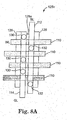
- Figure 8A illustrates a top view
- Figure 8B illustrates a side view of another embodiment of a layout 125c for single gate phase-change memory cells.
- Layout 125c is similar to layout 125a except that in layout 125c each phase-change element 106 is between a transistor 108 and a ground line 114 instead of between a transistor 108 and a bit line 112.
- Bit line 112 and ground line 114 are in separate metallization layers.
- bit line 112 is in a higher metallization layer than ground line 114.
- bit line 112 is in a lower metallization layer than ground line 114.
- Bit line 112 is parallel to ground line 114 and spaced apart from ground line 114 by a width as indicated at 128a.
- each transistor 108 One side of the source-drain path of each transistor 108 is electrically coupled to ground line 114 through a phase-change element 106 and contact 130. The other side of the source-drain path of each transistor 108 is electrically coupled to a bit line 112 through contact 132. The gate of each transistor 108 is electrically coupled to a word line 110.
- phase-change element 106 By locating phase-change element 106 in the back end of the line, the temperature budget available for processing of the lower metallization is improved.
- the improved temperature budget provides more options in selecting materials and processing methods.
- width 128a can be reduced to approximately zero to reduce the phase-change memory cell 104 size and therefore increase the density of the array of phase-change memory cells 100.
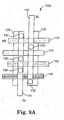
- Figure 9A illustrates a top view
- Figure 9B illustrates a side view of another embodiment of a layout 125d for single gate phase-change memory cells.
- Layout 125d is similar to layout 125c except that in layout 125d bit line 112 and ground line 114 are in the same metallization layer and the width 128b of the space between bit line 112 and ground line 114 is greater than width 128a (Fig. 8A). Since bit line 112 and ground line 114 are in the same metallization layer, width 128b is greater than width 128a to provide adequate isolation between bit line 112 and ground line 114.
- bit line 112 and ground line 114 By locating bit line 112 and ground line 114 in the same metallization layer, the resistance/length of bit line 112 and ground line 114 is easier to equalize than if bit line 112 and ground line 114 are in separate metallization layers. To equalize the resistance/length of bit line 112 and ground line 114 in the same metallization layer, the thickness of bit line 112 is made substantially equal to the thickness of ground line 114.
- Embodiments of the present invention provide phase-change memory array layouts for equalizing the parasitic series resistance due to bit lines and ground lines at each phase-change memory cell.
- the parasitic series resistance is equalized since the ground lines and bit lines are parallel to each other and are connected at opposite sides of the memory array.
- the layout of the phase-change memory cells can vary by locating the phase-change memory element between the transistor and the bit line or between the transistor and the ground line.
- the layout of the phase-change memory cells can also vary by locating the ground line and the bit line in the same metallization layer or in separate metallization layers.
- the embodiments provide an improved phase-change memory cell resistance distribution.
Landscapes
- Chemical & Material Sciences (AREA)
- Crystallography & Structural Chemistry (AREA)
- Semiconductor Memories (AREA)
- Static Random-Access Memory (AREA)
Abstract
Description
- Phase-change materials exhibit at least two different states. The states of phase-change material may be referenced to as amorphous and crystalline states. The states may be distinguished because the amorphous state generally exhibits higher resistivity than does the crystalline state. Generally, the amorphous state involves a more disordered atomic structure, while the crystalline state is an ordered lattice. Some phase-change materials exhibit two crystalline states, e.g. a face-centered cubic (FCC) state and a hexagonal closest packing (HCP) state. These two crystalline states have different resistivities. In the following description, the amorphous state generally refers to the state having the higher resistivity, and the crystalline state generally refers to the state having the lower resistivity.
- Phase change in the phase-change materials may be induced reversibly. In this way, the phase-change material may change from the amorphous state to the crystalline state, and from the crystalline state to the amorphous state, in response to temperature changes. The temperature changes to the phase-change material may be achieved in a variety of ways. For example, a laser can be directed to the phase-change material, current may be driven through the phase-change material, or current can be fed through a resistive heater adjacent the phase-change material. With any of these methods, controllable heating of the phase-change material causes controllable phase change within the phase-change material.
- An array of phase-change memory cells includes bit line and ground line wiring. Since the bit line and ground line wiring have a parasitic resistance, the set and reset current fed through a phase-change memory cell during the application of a voltage write pulse depends on the location of the phase-change memory cell in the memory array. This location dependent set and reset current contributes to a broadening of the phase-change memory cell resistance distribution and thereby affects the reliability of the phase-change memory cell set and reset operations. Typical solutions to this problem attempt to minimize the resistance or adjust the set and reset current based on the location of the phase-change memory cell within the memory array to compensate for the voltage drop over the bit line. These methods increase the costs of the phase-change memory due to increased process complexity and chip complexity.
- One embodiment of the present invention provides a memory. The memory includes memory cells, a first line coupled to the memory cells, and a second line coupled to the memory cells. A series resistance of the first line plus the second line at each one of the memory cells is substantially equal.
- Embodiments of the invention are better understood with reference to the following drawings. The elements of the drawings are not necessarily to scale relative to each other. Like reference numerals designate corresponding similar parts.
- Figure 1 is a diagram illustrating one embodiment of a memory.
- Figure 2A illustrates a top view of one embodiment of a layout for dual gate phase-change memory cells.
- Figure 2B illustrates a side view of one embodiment of a layout for dual gate phase-change memory cells.
- Figure 3A illustrates a top view of another embodiment of a layout for dual gate phase-change memory cells.
- Figure 3B illustrates a side view of another embodiment of a layout for dual gate phase-change memory cells.
- Figure 4A illustrates a top view of another embodiment of a layout for dual gate phase-change memory cells.
- Figure 4B illustrates a side view of another embodiment of a layout for dual gate phase-change memory cells.
- Figure 5A illustrates a top view of another embodiment of a layout for dual gate phase-change memory cells.
- Figure 5B illustrates a side view of another embodiment of a layout for dual gate phase-change memory cells.
- Figure 6A illustrates a top view of one embodiment of a layout for single gate phase-change memory cells.
- Figure 6B illustrates a side view of one embodiment of a layout for single gate phase-change memory cells.
- Figure 7A illustrates a top view of another embodiment of a layout for single gate phase-change memory cells.
- Figure 7B illustrates a side view of another embodiment of a layout for single gate phase-change memory cells.
- Figure 8A illustrates a top view of another embodiment of a layout for single gate phase-change memory cells.
- Figure 8B illustrates a side view of another embodiment of a layout for single gate phase-change memory cells.
- Figure 9A illustrates a top view of another embodiment of a layout for single gate phase-change memory cells.
- Figure 9B illustrates a side view of another embodiment of a layout for single gate phase-change memory cells.
- Figure 1 is a diagram illustrating one embodiment of a
memory 100.Memory 100 include a plurality of phase-change memory cells 104a-104d (collectively referred to as phase-change memory cells 104), a plurality offirst lines 112a-112b (collectively referred to as first lines 112), a plurality of select lines 110a-110b (collectively referred to as select lines 110), and a plurality ofsecond lines 114a-114b (collectively referred to as second lines 114). Each phase-change memory cell 104 is electrically coupled to aselect line 110, afirst line 112, and asecond line 114. While phase-change memory cells 104 are used in the illustrated embodiment, in other embodiments, other suitable types of memory cells can be used. In the following description,first lines 112 are referred to asbit lines 112,second lines 114 are referred to asground lines 114, andselect lines 110 are referred to asword lines 110 due to the use of phase-change element 106 and field-effect transistor (FET) 108 within phase-change memory cell 104. Thus, phase-change memory cell 104c is electrically coupled to bit line (BL) 112b, word line (WL1) 110a, and ground line (GL) 114b, and phase-change memory cell 104d is electrically coupled tobit line 112b, word line (WL2) 110b, andground line 114b. - The set and reset current fed through a phase-change memory cell 104 of phase-change
memory cell array 100 does not depend on the location of the phase-change memory cell inmemory array 100.Memory array 100 balances the unavoidable, position dependent voltage drop overbit lines 112 by a voltage drop overground lines 114, which has the inverse location dependence such that the total series resistance due to the wiring is constant for each phase-change memory cell 104 inmemory array 100. The total series resistance for each phase-change memory cell 104 is made equal by the parallel routing ofbit lines 112 andground lines 114 and the connection ofbit lines 112 andground lines 114 atopposite sides memory array 100, respectively, so that the total wiring length inmemory array 100 is the same for each phase-change memory cell 104. - To equalize the series resistance due to the bit line and ground line wiring, each
bit line 112 and eachground line 114 has the same resistance per length (resistance/length). The same resistance/length can be achieved by a reduction in thickness of the higher metallization line (e.g., Al, Cu) which typically has a lower resistivity than lower metallization levels (e.g., W). In one embodiment,bit lines 112 andground lines 114 inmemory array 100 run in parallel and the line resistance ofbit lines 112 and the line resistance ofground lines 114 are approximately equal so that the actual write voltage of an individual phase-change memory cell 104 is not dependent on the position of phase-change memory cell 104 inmemory array 100. This is due to a constant sum of the voltage drop overbit line 112 andground line 114 for each phase-change memory cell 104. In one embodiment,memory array 100 includes twomemory cells bit line 112a andground line 114a run in parallel and the line resistance ofbit line 112a and the line resistance ofground line 114a are approximately equal. In other embodiments, one or more of thebit lines 112 have an orientation to one or more of theground lines 114 that is not parallel. - In the illustrated embodiment, each phase-change memory cell 104 includes a phase-
change element 106 and atransistor 108. Whiletransistor 108 is a FET in the illustrated embodiment, in other embodiments,transistor 108 can be other suitable devices such as a bipolar transistor or a 3D transistor structure. In the illustrated embodiment, phase-change memory cell 104c includes phase-change element 106a andtransistor 108a. One side of phase-change element 106a is electrically coupled tobit line 112b and the other side of phase-change element 106a is electrically coupled to one side of the source-drain path oftransistor 108a. The other side of the source-drain path oftransistor 108a is electrically coupled toground line 114b. The gate oftransistor 108a is electrically coupled to word line 110a. Phase-change memory cell 104d includes phase-change element 106b andtransistor 108b. One side of phase-change element 106b is electrically coupled tobit line 112b and the other side of phase-change element 106b is electrically coupled to one side of the source-drain path oftransistor 108b. The other side of the source-drain path oftransistor 108b is electrically coupled toground line 114b. The gate oftransistor 108b is electrically coupled toword line 110b. - In various embodiments, each phase-
change element 106 comprises a phase-change material that may be made up of a variety of suitable materials in accordance with the present invention. Generally, chalcogenide alloys that contain one or more elements from group VI of the periodic table are useful as such materials. In one embodiment, the phase-change material of phase-change element 106 is made up of a chalcogenide compound material, such as GeSbTe, SbTe, or AgInSbTe. In another embodiment, the phase-change material can be chalcogen free, such as GeSb, GaSb, or GeGaSb. - In the illustrated embodiment,
bit lines 112 are connected to additional circuits on oneside 102 ofmemory array 100, andground lines 114 are connected to additional circuits on anotherside 103 ofmemory array 100.Side 102 ofmemory array 100 isopposite side 103 ofmemory array 100. In one embodiment,bit lines 112 are parallel to groundlines 114. In other embodiments,bit lines 112 can have other suitable orientations to groundlines 114. In the illustrated embodiment, the length ofbit line 112b from phase-change memory cell 104c toside 102 ofmemory array 100 is indicated at 118, and the length ofbit line 112b from phase-change memory cell 104d toside 102 ofmemory array 100 is indicated at 116. The length ofground line 114b from phase-change memory cell 104c toside 103 ofmemory array 100 is indicated at 120, and the length ofground line 114b from phase-change memory cell 104d toside 103 ofmemory array 100 is indicated at 122. - In the illustrated embodiment, the
length 118 ofbit line 112b from phase-change memory cell 104c toside 102 ofmemory array 100 plus thelength 120 ofground line 114b from phase-change memory cell 104c toside 103 ofmemory array 100 is equal to thelength 116 ofbit line 112b frommemory cell 104d toside 102 ofmemory array 100 plus thelength 122 ofground line 114b from phase-change memory cell 104d toside 103 ofmemory array 100. In this embodiment,bit line 112b andground line 114b have the same resistance/length so that the series resistance due tobit line 112b andground line 114b are equal for both phase-change memory cells bit line 112b andground line 114b such that the series resistance due tobit line 112b andground line 114b are equal for both phase-change memory cells - In the illustrated embodiment, the series resistance due to
bit lines 112 andground lines 114 for each phase-change memory cell 104 inmemory array 100 is substantially equal. Therefore, the write current and/or voltage for setting or resetting a phase-change memory cell 104 is the same for all phase-change memory cells 104 inmemory array 100. While four memory cells 104 are illustrated in Figure 1, in other embodiments, two memory cells 104 are used and are coupled to thesame bit line 112 andground line 114. - In the illustrated embodiment, during a set operation for phase-
change memory cell 104c, a set current and/or voltage pulse is selectively enabled and sent throughbit line 112b to phase-change element 106a thereby heating it above it's crystallization temperature (but usually below it's melting temperature) with word line 110a selected to activatetransistor 108a. In this way, phase-change element 106a reaches its crystalline state during this set operation. During a reset operation of phase-change memory cell 104c, a reset current and/or voltage pulse is selectively enabled tobit line 112b and sent to phase-change material element 106a. The reset current or voltage quickly heats phase-change element 106a above its melting temperature. After the current and/or voltage pulse is turned off, the phase-change element 106a quickly quench cools into the amorphous state. Phase-change memory cell 104d and other phase-change memory cells 104 inarray 100 are set and reset similarly to phase-change memory cell 104c using the same current and/or voltage pulse value. - Figure 2A illustrates a top view and Figure 2B illustrates a side view of one embodiment of a
layout 124a for dual gate phase-change memory cells. Dual gate phase-change memory cells include twotransistors 108 that are both shared and support one phase-change element 106.Layout 124a includessubstrate 136,bit line 112,ground line 114, shallow trench isolation (STI) 126, word lines 110,transistors 108,contacts 130,contacts 132, and phase-change elements 106.Bit line 112 andground line 114 are in separate metallization layers. In one embodiment,bit line 112 comprises W or another suitable metal and is in a lower metallization layer thanground line 114, which comprises Al, Cu, or another suitable metal. In another embodiment,bit line 112 comprises Al, Cu, or another suitable metal and is in a higher metallization layer thanground line 114, which comprises W or another suitable metal. In one embodiment,bit line 112 andground line 114 have substantially the same resistance/length. -
Bit line 112 is spaced apart fromground line 114 by a width as indicated at 128a. In one embodiment,bit line 112 is parallel toground line 114. One side of the source-drain path of eachtransistor 108 is electrically coupled toground line 114 through acontact 132, which comprises Cu, W, or another suitable conductive material. The other side of the source-drain path of eachtransistor 108 is electrically coupled to abit line 112 through a phase-change element 106 and contact 130, which comprises Cu, W, or another suitable electrically conductive material. The gate of eachtransistor 108 is electrically coupled to aword line 110, which comprises doped poly-Si, W, TiN, or another suitable material. In this embodiment, phase-change elements 106 are located betweentransistor 108 andbit line 112. In various embodiments,memory element 106 is a heater cell, an active-in-via cell, a pillar cell, or other suitable phase-change memory element. In the illustrated embodiment, by locatingbit line 112 andground line 114 in separate metallization layers,width 128a can be reduced to approximately zero to reduce the phase-change memory cell 104 size and therefore increase the density of the array of phase-change memory cells 100. - Figure 3A illustrates a top view and Figure 3B illustrates a side view of another embodiment of a
layout 124b for dual gate phase-change memory cells.Layout 124b is similar tolayout 124a except that inlayout 124b bitline 112 andground line 114 are in the same metallization layer and thewidth 128b of the space betweenbit line 112 andground line 114 is greater thanwidth 128a (Fig. 2A). Sincebit line 112 andground line 114 are in the same metallization layer,width 128b is greater thanwidth 128a to provide adequate isolation betweenbit line 112 andground line 114. By locatingbit line 112 andground line 114 in the same metallization layer, the resistance/length ofbit line 112 andground line 114 is easier to equalize than ifbit line 112 andground line 114 are in separate metallization layers. To equalize the resistance/length ofbit line 112 andground line 114 in the same metallization layer, the thickness ofbit line 112 is made substantially equal to the thickness ofground line 114. - Figure 4A illustrates a top view and Figure 4B illustrates a side view of another embodiment of a
layout 124c for dual gate phase-change memory cells.Layout 124c is similar tolayout 124a except that inlayout 124c phase-change element 106 is between atransistor 108 andground line 114 instead of between atransistor 108 and abit line 112.Bit line 112 andground line 114 are in separate metallization layers. In one embodiment,bit line 112 is in a higher metallization layer thanground line 114. In another embodiment,bit line 112 is in a lower metallization layer thanground line 114.Bit line 112 is parallel toground line 114 and spaced apart fromground line 114 by a width as indicated at 128a. One side of the source-drain path of eachtransistor 108 is electrically coupled toground line 114 through a phase-change element 106 and contact 130. The other side of the source-drain path of eachtransistor 108 is electrically coupled to abit line 112 throughcontact 132. The gate of eachtransistor 108 is electrically coupled to aword line 110. - By fabricating phase-
change element 106 after one or more of the metallization layers are deposited, the temperature budget available for processing these one or more metallization layers is improved. The improved temperature budget provides more options in selecting materials and processing methods. By locatingbit line 112 andground line 114 in separate metallization layers,width 128a can be reduced to approximately zero to reduce the phase-change memory cell 104 size and therefore increase the density of the array of phase-change memory cells 100. - Figure 5A illustrates a top view and Figure 5B illustrates a side view of another embodiment of a
layout 124d for dual gate phase-change memory cells.Layout 124d is similar tolayout 124c except that inlayout 124d bit line 112 andground line 114 are in the same metallization layer and thewidth 128b of the space betweenbit line 112 andground line 114 is greater thanwidth 128a (Fig. 4A). Sincebit line 112 andground line 114 are in the same metallization layer,width 128b is greater thanwidth 128a to provide adequate isolation betweenbit line 112 andground line 114. By locatingbit line 112 andground line 114 in the same metallization layer, the resistance/length ofbit line 112 andground line 114 is easier to equalize than ifbit line 112 andground line 114 are in separate metallization layers. To equalize the resistance/length ofbit line 112 andground line 114 in the same metallization layer, the thickness ofbit line 112 is made substantially equal to the thickness ofground line 114. - Figure 6A illustrates a top view and Figure 6B illustrates a side view of one embodiment of a
layout 125a for single gate phase-change memory cells. Single gate phase-change memory cells include onetransistor 108 to support one phase-change element 106.Layout 125a includessubstrate 136,bit line 112,ground line 114, shallow trench isolation (STI) 126, word lines 110,transistors 108,contacts 130,contacts 132, and phase-change elements 106.Bit line 112 andground line 114 are in separate metallization layers. In one embodiment,bit line 112 is in a higher metallization layer thanground line 114. In another embodiment,bit line 112 is in a lower metallization layer thanground line 114. -
Bit line 112 is parallel toground line 114 and spaced apart fromground line 114 by a width as indicated at 128a. One side of the source-drain path of eachtransistor 108 is electrically coupled toground line 114 through acontact 132. The other side of the source-drain path of eachtransistor 108 is electrically coupled to abit line 112 through a phase-change element 106 and contact 130. The gate of eachtransistor 108 is electrically coupled to aword line 110. In this embodiment, each phase-change element 106 is located between atransistor 108 and abit line 112. In one embodiment,memory element 106 is a heater cell, an active-in-via cell, a pillar cell, or other suitable phase-change memory element. By locatingbit line 112 andground line 114 in separate metallization layers,width 128a can be reduced to approximately zero to reduce the phase-change memory cell 104 size and therefore increase the density of the array of phase-change memory cells 100. - Figure 7A illustrates a top view and Figure 7B illustrates a side view of another embodiment of a
layout 125b for single gate phase-change memory cells.Layout 125b is similar tolayout 125a except that inlayout 125b bitline 112 andground line 114 are in the same metallization layer and thewidth 128b of the space betweenbit line 112 andground line 114 is greater thanwidth 128a (Fig. 6A). Sincebit line 112 andground line 114 are in the same metallization layer,width 128b is greater thanwidth 128a to provide adequate isolation betweenbit line 112 andground line 114. By locatingbit line 112 andground line 114 in the same metallization layer, the resistance/length ofbit line 112 andground line 114 is easier to equalize than ifbit line 112 andground line 114 are in separate metallization layers. To equalize the resistance/length ofbit line 112 andground line 114 in the same metallization layer, the thickness ofbit line 112 is made substantially equal to the thickness ofground line 114. - Figure 8A illustrates a top view and Figure 8B illustrates a side view of another embodiment of a
layout 125c for single gate phase-change memory cells.Layout 125c is similar tolayout 125a except that inlayout 125c each phase-change element 106 is between atransistor 108 and aground line 114 instead of between atransistor 108 and abit line 112.Bit line 112 andground line 114 are in separate metallization layers. In one embodiment,bit line 112 is in a higher metallization layer thanground line 114. In another embodiment,bit line 112 is in a lower metallization layer thanground line 114.Bit line 112 is parallel toground line 114 and spaced apart fromground line 114 by a width as indicated at 128a. One side of the source-drain path of eachtransistor 108 is electrically coupled toground line 114 through a phase-change element 106 and contact 130. The other side of the source-drain path of eachtransistor 108 is electrically coupled to abit line 112 throughcontact 132. The gate of eachtransistor 108 is electrically coupled to aword line 110. - By locating phase-
change element 106 in the back end of the line, the temperature budget available for processing of the lower metallization is improved. The improved temperature budget provides more options in selecting materials and processing methods. By locatingbit line 112 andground line 114 in separate metallization layers,width 128a can be reduced to approximately zero to reduce the phase-change memory cell 104 size and therefore increase the density of the array of phase-change memory cells 100. - Figure 9A illustrates a top view and Figure 9B illustrates a side view of another embodiment of a
layout 125d for single gate phase-change memory cells.Layout 125d is similar tolayout 125c except that inlayout 125d bit line 112 andground line 114 are in the same metallization layer and thewidth 128b of the space betweenbit line 112 andground line 114 is greater thanwidth 128a (Fig. 8A). Sincebit line 112 andground line 114 are in the same metallization layer,width 128b is greater thanwidth 128a to provide adequate isolation betweenbit line 112 andground line 114. By locatingbit line 112 andground line 114 in the same metallization layer, the resistance/length ofbit line 112 andground line 114 is easier to equalize than ifbit line 112 andground line 114 are in separate metallization layers. To equalize the resistance/length ofbit line 112 andground line 114 in the same metallization layer, the thickness ofbit line 112 is made substantially equal to the thickness ofground line 114. - Embodiments of the present invention provide phase-change memory array layouts for equalizing the parasitic series resistance due to bit lines and ground lines at each phase-change memory cell. The parasitic series resistance is equalized since the ground lines and bit lines are parallel to each other and are connected at opposite sides of the memory array. The layout of the phase-change memory cells can vary by locating the phase-change memory element between the transistor and the bit line or between the transistor and the ground line. The layout of the phase-change memory cells can also vary by locating the ground line and the bit line in the same metallization layer or in separate metallization layers. The embodiments provide an improved phase-change memory cell resistance distribution.
Claims (25)
- A memory comprising:memory cells;a first line coupled to the memory cells; anda second line coupled to the memory cells,wherein a series resistance of the first line plus the second line at each one of the memory cells is substantially equal.
- The memory of claim 1, wherein the first line and the second line have substantially the same resistance per unit length.
- The memory of claim 1, wherein the first line and the second line are located in separate metallization layers.
- The memory of claim 1, wherein the first line and the second line are located in a same metallization layer.
- The memory of claim 1, wherein the memory cells each comprise a phase-change element.
- The memory of claim 1, wherein the memory cells each comprise a transistor coupled to a phase-change element, and wherein the transistor and the phase-change element for each one of the memory cells are coupled between the first line and the second line.
- A memory comprising:an array of phase-change memory cells;bit lines coupled to each of the phase-change memory cells; andground lines parallel to the bit lines and coupled to each of the phase-change memory cells,wherein the bit lines are connected at a first side of the array of phase-change memory cells and the ground lines are connected at a second side of the array of phase-change memory cells opposite the first side, andwherein the bit lines and the ground lines have substantially the same resistance/length.
- The memory of claim 7, wherein the bit lines are located in a first metallization layer and the ground lines are located in a second metallization layer.
- The memory of claim 7, wherein the bit lines and the ground lines are located in a same metallization layer.
- The memory of claim 7, wherein each phase-change memory cell comprises a transistor and a phase-change element coupled between the transistor and a bit line.
- The memory of claim 7, wherein each phase-change memory cell comprises a transistor and a phase change element coupled between the transistor and a ground line.
- A memory comprising:an array of phase-change memory cells;bit lines coupled to corresponding phase-change memory cells;ground lines coupled to corresponding phase-change memory cells; andmeans for equalizing a parasitic series resistance for each phase-change memory cell due to the bit lines and the ground lines.
- The memory of claim 12, further comprising:means for equalizing a resistance/length of the bit lines and the ground lines.
- A method for writing a memory comprising:providing a plurality of phase-change memory cells;providing a bit line coupled to each of the phase-change memory cells;providing a ground line parallel to the bit line and coupled to each of the phase-change memory cells; andwriting to at least two of the phase-change memory cells using a constant write pulse, wherein a voltage drop over the bit line and the ground line during the write pulse is substantially the same for the at least two phase-change memory cells.
- The method of claim 14, wherein providing the plurality of phase-change memory cells comprises providing a plurality of dual gate phase-change memory cells.
- The method of claim 14, wherein providing the plurality of phase-change memory cells comprises providing a plurality of single gate phase-change memory cells.
- The method of claim 14, wherein providing the plurality of phase-change memory cells comprises providing a plurality of phase-change memory cells having a phase-change element at the bit line.
- The method of claim 14, wherein providing the plurality of phase-change memory cells comprises providing a plurality of phase-change memory cells having a phase-change element at the ground line.
- The method of claim 14, wherein providing the ground line comprises providing the ground line in the same metallization layer as the bit line.
- The method of claim 14, wherein providing the ground line comprises providing the ground line in a separate metallization layer than the bit line.
- A method for fabricating a memory, the method comprising:providing an array of phase-change memory cells;providing bit lines coupled to each of the phase-change memory cells;providing ground lines parallel to the bit lines and coupled to each of the phase-change memory cells;connecting the bit lines to a first side of the array of phase-change memory cells; andconnecting the ground lines to a second side of the array of phase-change memory cells opposite the first side,wherein the bit lines and the ground lines have substantially the same resistance/length.
- The memory of claim 21, wherein providing the bit lines comprises providing the bit lines in a separate metallization layer from the ground lines.
- The memory of claim 21, wherein providing the ground lines comprises providing the ground lines in a same metallization layer as the bit lines.
- The memory of claim 21, wherein providing the array of phase-change memory cells comprises providing a transistor and a phase-change element between the transistor and a bit line for each phase-change memory cell.
- The memory of claim 21, wherein providing the array of phase-change memory cells comprises providing a transistor and a phase change element between the transistor and a ground line for each phase-change memory cell.
Applications Claiming Priority (1)
| Application Number | Priority Date | Filing Date | Title |
|---|---|---|---|
| US11/210,525 US7339814B2 (en) | 2005-08-24 | 2005-08-24 | Phase change memory array having equalized resistance |
Publications (3)
| Publication Number | Publication Date |
|---|---|
| EP1758167A2 true EP1758167A2 (en) | 2007-02-28 |
| EP1758167A3 EP1758167A3 (en) | 2008-03-26 |
| EP1758167B1 EP1758167B1 (en) | 2011-01-12 |
Family
ID=37507813
Family Applications (1)
| Application Number | Title | Priority Date | Filing Date |
|---|---|---|---|
| EP06016871A Not-in-force EP1758167B1 (en) | 2005-08-24 | 2006-08-11 | Phase change memory array having equalized resistance |
Country Status (3)
| Country | Link |
|---|---|
| US (1) | US7339814B2 (en) |
| EP (1) | EP1758167B1 (en) |
| DE (1) | DE602006019525D1 (en) |
Families Citing this family (6)
| Publication number | Priority date | Publication date | Assignee | Title |
|---|---|---|---|---|
| JP4231502B2 (en) * | 2005-11-02 | 2009-03-04 | シャープ株式会社 | Semiconductor memory device with cross-point structure |
| JP2008053494A (en) * | 2006-08-25 | 2008-03-06 | Elpida Memory Inc | Semiconductor device and manufacturing method thereof |
| US7817454B2 (en) * | 2007-04-03 | 2010-10-19 | Micron Technology, Inc. | Variable resistance memory with lattice array using enclosing transistors |
| US7889536B2 (en) * | 2007-12-17 | 2011-02-15 | Qimonda Ag | Integrated circuit including quench devices |
| RU2702271C2 (en) * | 2015-06-10 | 2019-10-07 | Тосиба Мемори Корпорейшн | Memory device with change of resistance |
| CN114695355A (en) * | 2020-12-29 | 2022-07-01 | 长鑫存储技术有限公司 | Semiconductor structure and method for forming semiconductor structure |
Family Cites Families (4)
| Publication number | Priority date | Publication date | Assignee | Title |
|---|---|---|---|---|
| US5825683A (en) * | 1997-10-29 | 1998-10-20 | Utron Technology Inc. | Folded read-only memory |
| US6456525B1 (en) * | 2000-09-15 | 2002-09-24 | Hewlett-Packard Company | Short-tolerant resistive cross point array |
| JP4242117B2 (en) * | 2002-07-11 | 2009-03-18 | 株式会社ルネサステクノロジ | Storage device |
| JP2004158119A (en) * | 2002-11-06 | 2004-06-03 | Sharp Corp | Nonvolatile semiconductor memory device |
-
2005
- 2005-08-24 US US11/210,525 patent/US7339814B2/en not_active Expired - Lifetime
-
2006
- 2006-08-11 DE DE602006019525T patent/DE602006019525D1/en active Active
- 2006-08-11 EP EP06016871A patent/EP1758167B1/en not_active Not-in-force
Also Published As
| Publication number | Publication date |
|---|---|
| EP1758167B1 (en) | 2011-01-12 |
| EP1758167A3 (en) | 2008-03-26 |
| US7339814B2 (en) | 2008-03-04 |
| US20070053221A1 (en) | 2007-03-08 |
| DE602006019525D1 (en) | 2011-02-24 |
Similar Documents
| Publication | Publication Date | Title |
|---|---|---|
| US7817464B2 (en) | Phase change memory cell employing a GeBiTe layer as a phase change material layer, phase change memory device including the same, electronic system including the same and method of fabricating the same | |
| KR100807677B1 (en) | Phase change memory fabricated using self-aligned processing | |
| US7738279B2 (en) | Integrated circuit and method of operating an integrated circuit | |
| US7786464B2 (en) | Integrated circuit having dielectric layer including nanocrystals | |
| US7875492B2 (en) | Integrated circuit including a memory fabricated using self-aligned processing | |
| US8389973B2 (en) | Memory using tunneling field effect transistors | |
| US7558100B2 (en) | Phase change memory devices including memory cells having different phase change materials and related methods and systems | |
| US7545668B2 (en) | Mushroom phase change memory having a multilayer electrode | |
| US8284596B2 (en) | Integrated circuit including an array of diodes coupled to a layer of resistance changing material | |
| EP4007000B1 (en) | Semiconductor apparatus | |
| US8178379B2 (en) | Integrated circuit, resistivity changing memory device, memory module, and method of fabricating an integrated circuit | |
| US8039299B2 (en) | Method for fabricating an integrated circuit including resistivity changing material having a planarized surface | |
| US7977661B2 (en) | Memory having shared storage material | |
| US20080303015A1 (en) | Memory having shared storage material | |
| CN1971932B (en) | Semiconductor memory device | |
| WO2007090648A1 (en) | Memory having nanotube transistor access device | |
| US20080273369A1 (en) | Integrated Circuit, Memory Module, Method of Operating an Integrated Circuit, and Computing System | |
| EP1758167B1 (en) | Phase change memory array having equalized resistance | |
| US7528402B2 (en) | Electrically rewritable non-volatile memory element | |
| EP1848047A2 (en) | Transitioning the state of phase change material by annealing | |
| US7696510B2 (en) | Integrated circuit including memory having reduced cross talk |
Legal Events
| Date | Code | Title | Description |
|---|---|---|---|
| PUAI | Public reference made under article 153(3) epc to a published international application that has entered the european phase |
Free format text: ORIGINAL CODE: 0009012 |
|
| 17P | Request for examination filed |
Effective date: 20060811 |
|
| AK | Designated contracting states |
Kind code of ref document: A2 Designated state(s): AT BE BG CH CY CZ DE DK EE ES FI FR GB GR HU IE IS IT LI LT LU LV MC NL PL PT RO SE SI SK TR |
|
| AX | Request for extension of the european patent |
Extension state: AL BA HR MK YU |
|
| PUAL | Search report despatched |
Free format text: ORIGINAL CODE: 0009013 |
|
| AK | Designated contracting states |
Kind code of ref document: A3 Designated state(s): AT BE BG CH CY CZ DE DK EE ES FI FR GB GR HU IE IS IT LI LT LU LV MC NL PL PT RO SE SI SK TR |
|
| AX | Request for extension of the european patent |
Extension state: AL BA HR MK YU |
|
| AKX | Designation fees paid |
Designated state(s): DE FR GB |
|
| 17Q | First examination report despatched |
Effective date: 20081230 |
|
| 19U | Interruption of proceedings before grant |
Effective date: 20090401 |
|
| 19W | Proceedings resumed before grant after interruption of proceedings |
Effective date: 20091123 |
|
| GRAP | Despatch of communication of intention to grant a patent |
Free format text: ORIGINAL CODE: EPIDOSNIGR1 |
|
| RIC1 | Information provided on ipc code assigned before grant |
Ipc: G11C 16/02 20060101ALI20100609BHEP Ipc: H01L 27/24 20060101ALI20100609BHEP Ipc: H01L 27/105 20060101AFI20100609BHEP |
|
| GRAS | Grant fee paid |
Free format text: ORIGINAL CODE: EPIDOSNIGR3 |
|
| GRAA | (expected) grant |
Free format text: ORIGINAL CODE: 0009210 |
|
| AK | Designated contracting states |
Kind code of ref document: B1 Designated state(s): DE FR GB |
|
| REG | Reference to a national code |
Ref country code: GB Ref legal event code: FG4D |
|
| REF | Corresponds to: |
Ref document number: 602006019525 Country of ref document: DE Date of ref document: 20110224 Kind code of ref document: P |
|
| REG | Reference to a national code |
Ref country code: DE Ref legal event code: R096 Ref document number: 602006019525 Country of ref document: DE Effective date: 20110224 |
|
| PLBE | No opposition filed within time limit |
Free format text: ORIGINAL CODE: 0009261 |
|
| STAA | Information on the status of an ep patent application or granted ep patent |
Free format text: STATUS: NO OPPOSITION FILED WITHIN TIME LIMIT |
|
| 26N | No opposition filed |
Effective date: 20111013 |
|
| REG | Reference to a national code |
Ref country code: DE Ref legal event code: R097 Ref document number: 602006019525 Country of ref document: DE Effective date: 20111013 |
|
| GBPC | Gb: european patent ceased through non-payment of renewal fee |
Effective date: 20110811 |
|
| REG | Reference to a national code |
Ref country code: FR Ref legal event code: ST Effective date: 20120430 |
|
| PG25 | Lapsed in a contracting state [announced via postgrant information from national office to epo] |
Ref country code: FR Free format text: LAPSE BECAUSE OF NON-PAYMENT OF DUE FEES Effective date: 20110831 Ref country code: GB Free format text: LAPSE BECAUSE OF NON-PAYMENT OF DUE FEES Effective date: 20110811 |
|
| REG | Reference to a national code |
Ref country code: DE Ref legal event code: R081 Ref document number: 602006019525 Country of ref document: DE Owner name: INFINEON TECHNOLOGIES AG, DE Free format text: FORMER OWNER: QIMONDA AG, 81739 MUENCHEN, DE |
|
| PGFP | Annual fee paid to national office [announced via postgrant information from national office to epo] |
Ref country code: DE Payment date: 20221021 Year of fee payment: 17 |
|
| P01 | Opt-out of the competence of the unified patent court (upc) registered |
Effective date: 20230528 |
|
| REG | Reference to a national code |
Ref country code: DE Ref legal event code: R119 Ref document number: 602006019525 Country of ref document: DE |
|
| PG25 | Lapsed in a contracting state [announced via postgrant information from national office to epo] |
Ref country code: DE Free format text: LAPSE BECAUSE OF NON-PAYMENT OF DUE FEES Effective date: 20240301 |