EP1755168A2 - Deep N diffusion for trench IGBT - Google Patents
Deep N diffusion for trench IGBT Download PDFInfo
- Publication number
- EP1755168A2 EP1755168A2 EP06016715A EP06016715A EP1755168A2 EP 1755168 A2 EP1755168 A2 EP 1755168A2 EP 06016715 A EP06016715 A EP 06016715A EP 06016715 A EP06016715 A EP 06016715A EP 1755168 A2 EP1755168 A2 EP 1755168A2
- Authority
- EP
- European Patent Office
- Prior art keywords
- trenches
- diffusion
- microns
- emitter
- depth
- Prior art date
- Legal status (The legal status is an assumption and is not a legal conclusion. Google has not performed a legal analysis and makes no representation as to the accuracy of the status listed.)
- Withdrawn
Links
- 238000009792 diffusion process Methods 0.000 title claims abstract description 36
- 230000001965 increasing effect Effects 0.000 claims abstract description 8
- 229910052710 silicon Inorganic materials 0.000 claims description 5
- 239000010703 silicon Substances 0.000 claims description 5
- 238000009413 insulation Methods 0.000 claims description 3
- 239000002184 metal Substances 0.000 claims 3
- 230000007480 spreading Effects 0.000 abstract description 5
- 239000007943 implant Substances 0.000 description 13
- 238000000034 method Methods 0.000 description 5
- 230000008569 process Effects 0.000 description 5
- XUIMIQQOPSSXEZ-UHFFFAOYSA-N Silicon Chemical compound [Si] XUIMIQQOPSSXEZ-UHFFFAOYSA-N 0.000 description 4
- 238000004519 manufacturing process Methods 0.000 description 3
- ZOXJGFHDIHLPTG-UHFFFAOYSA-N Boron Chemical compound [B] ZOXJGFHDIHLPTG-UHFFFAOYSA-N 0.000 description 2
- OAICVXFJPJFONN-UHFFFAOYSA-N Phosphorus Chemical compound [P] OAICVXFJPJFONN-UHFFFAOYSA-N 0.000 description 2
- VYPSYNLAJGMNEJ-UHFFFAOYSA-N Silicium dioxide Chemical compound O=[Si]=O VYPSYNLAJGMNEJ-UHFFFAOYSA-N 0.000 description 2
- 229910052796 boron Inorganic materials 0.000 description 2
- 239000000463 material Substances 0.000 description 2
- 229910052698 phosphorus Inorganic materials 0.000 description 2
- 239000011574 phosphorus Substances 0.000 description 2
- 229920002120 photoresistant polymer Polymers 0.000 description 2
- 229910021420 polycrystalline silicon Inorganic materials 0.000 description 2
- 229920005591 polysilicon Polymers 0.000 description 2
- XAGFODPZIPBFFR-UHFFFAOYSA-N aluminium Chemical compound [Al] XAGFODPZIPBFFR-UHFFFAOYSA-N 0.000 description 1
- 229910052782 aluminium Inorganic materials 0.000 description 1
- 229910052785 arsenic Inorganic materials 0.000 description 1
- RQNWIZPPADIBDY-UHFFFAOYSA-N arsenic atom Chemical compound [As] RQNWIZPPADIBDY-UHFFFAOYSA-N 0.000 description 1
- 230000015572 biosynthetic process Effects 0.000 description 1
- 230000001413 cellular effect Effects 0.000 description 1
- 229910052734 helium Inorganic materials 0.000 description 1
- 239000001307 helium Substances 0.000 description 1
- SWQJXJOGLNCZEY-UHFFFAOYSA-N helium atom Chemical compound [He] SWQJXJOGLNCZEY-UHFFFAOYSA-N 0.000 description 1
- 230000006872 improvement Effects 0.000 description 1
- 230000001939 inductive effect Effects 0.000 description 1
- 230000004048 modification Effects 0.000 description 1
- 238000012986 modification Methods 0.000 description 1
- 230000003647 oxidation Effects 0.000 description 1
- 238000007254 oxidation reaction Methods 0.000 description 1
- 230000003071 parasitic effect Effects 0.000 description 1
- 230000009467 reduction Effects 0.000 description 1
- 235000012239 silicon dioxide Nutrition 0.000 description 1
- 239000000377 silicon dioxide Substances 0.000 description 1
- 238000007669 thermal treatment Methods 0.000 description 1
Images


Classifications
-
- H—ELECTRICITY
- H10—SEMICONDUCTOR DEVICES; ELECTRIC SOLID-STATE DEVICES NOT OTHERWISE PROVIDED FOR
- H10D—INORGANIC ELECTRIC SEMICONDUCTOR DEVICES
- H10D10/00—Bipolar junction transistors [BJT]
-
- H—ELECTRICITY
- H10—SEMICONDUCTOR DEVICES; ELECTRIC SOLID-STATE DEVICES NOT OTHERWISE PROVIDED FOR
- H10D—INORGANIC ELECTRIC SEMICONDUCTOR DEVICES
- H10D12/00—Bipolar devices controlled by the field effect, e.g. insulated-gate bipolar transistors [IGBT]
- H10D12/01—Manufacture or treatment
- H10D12/031—Manufacture or treatment of IGBTs
- H10D12/032—Manufacture or treatment of IGBTs of vertical IGBTs
- H10D12/038—Manufacture or treatment of IGBTs of vertical IGBTs having a recessed gate, e.g. trench-gate IGBTs
-
- H—ELECTRICITY
- H10—SEMICONDUCTOR DEVICES; ELECTRIC SOLID-STATE DEVICES NOT OTHERWISE PROVIDED FOR
- H10D—INORGANIC ELECTRIC SEMICONDUCTOR DEVICES
- H10D12/00—Bipolar devices controlled by the field effect, e.g. insulated-gate bipolar transistors [IGBT]
- H10D12/411—Insulated-gate bipolar transistors [IGBT]
- H10D12/441—Vertical IGBTs
- H10D12/461—Vertical IGBTs having non-planar surfaces, e.g. having trenches, recesses or pillars in the surfaces of the emitter, base or collector regions
- H10D12/481—Vertical IGBTs having non-planar surfaces, e.g. having trenches, recesses or pillars in the surfaces of the emitter, base or collector regions having gate structures on slanted surfaces, on vertical surfaces, or in grooves, e.g. trench gate IGBTs
-
- H—ELECTRICITY
- H10—SEMICONDUCTOR DEVICES; ELECTRIC SOLID-STATE DEVICES NOT OTHERWISE PROVIDED FOR
- H10D—INORGANIC ELECTRIC SEMICONDUCTOR DEVICES
- H10D48/00—Individual devices not covered by groups H10D1/00 - H10D44/00
- H10D48/30—Devices controlled by electric currents or voltages
- H10D48/32—Devices controlled by only the electric current supplied, or only the electric potential applied, to an electrode which does not carry the current to be rectified, amplified or switched
- H10D48/34—Bipolar devices
Definitions
- This invention relates to trench type Insulated Gate Bipolar Transistors (IGBTs) and more specifically relates to such IGBTs with a reduced forward voltage drop.
- IGBTs Insulated Gate Bipolar Transistors
- IGBTs are well known and are frequently implemented with a planar cellular or stripe topology. These devices have an inherent JFET which increases the device on-resistance R DSON and, thus the forward voltage drop V CE(ON) . Further, such devices have an inherent four layer parasitic thyristor structure which will latch on if the NPN transistor of the thyristor turns on.
- IGBTs can be made with a trench topology which eliminates the inherent JFET of the planar device.
- trench IGBTs still have the inherent four layer structure whereby, if the inherent NPN transistor in the four layer device turns on (if the current through R B , is sufficiently high), the device will latch on. It is also desirable to reduce the saturation current of the device without increasing the value of R B .
- trench IGBTs tend to be "fragile", that is, they can fail particularly when switching an inductive load. This is sometimes termed a low safe operating area (SOA) under reverse bias. This problem again is aggravated by an increased R B' .
- SOA safe operating area
- U.S. Patent 6,683,331 the disclosure of which is incorporated herein by reference, describes a trench IGBT structure and process for its manufacture, creating a non-punch through (NPT) IGBT having a reduced R B' , a reduced saturation current, a low threshold voltage V T and an enlarged SOA. More specifically, a structure is .provided having a deep emitter diffusion which is very narrow (of small lateral extent) to reduce R B' . Further, a very deep P channel diffusion is employed between spaced trenches to create a very long inversion channel.
- NPT non-punch through
- the path for hole current under the emitter has a reduced lateral extent, reducing R B , and the trench is very deep (about 8 microns) so that the P region adjacent the channel can support reasonable voltage and the N- body concentration and depth can be optimized.
- the increased depth of the emitter along the trench controls threshold voltage since it permits the use of a very deep P + region without the danger of its encroaching into the channel (which would increase V T ).
- a helium implant may be employed for lifetime killing in only the P well.
- the device of the 6,683,331 patent may be built in float zone silicon and no epitaxial layer is needed, with a weak anode structure being employed as in copending application Serial No. 09/565,922, filed May 5, 2000 in the names of Richard Francis and Chiu Ng now U.S. patent 6,482,681 .
- the current during forward conduction can be seen as a combination of MOSFET and bipolar currents.
- the specific on-resistance to the MOSFET current is determined by several components.
- the major contribution of on resistance is from drift region resistance and spreading resistance below the channel region.
- the spreading and drift region resistance in a trench type IGBT is reduced by the introduction of a deep diffusion layer below the base diffusion.
- This deep diffusion or “Deep Enhancement” has an opposite doping concentration with respect to the P type base (or N type for an N channel device).
- the present invention reduces the device forward voltage drop by reducing on resistance. Further the invention provides the possibility to optimize the device to specific applications (e.g. switching frequency). Further, with the invention, in an high lifetime, epitaxial type trench IGBT, the irradiation dose can be increased to reduce the turn-off current and the switching time, hence reducing switching losses for the same forward drop. This is very useful in many applications, and significantly, in a low lifetime, depletion stop type trench IGBT, the deep enhancement of the invention will substantially reduce the device forward drop.
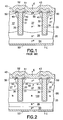
- Figure 1 is a cross-section through two adjacent trenches of an IGBT trench die having the junction pattern of the device of patent 6,683,331.
- Figure 2 is a cross-section like that of Figure 1, but showing the added novel deep enhancement of the invention.
- Figure 3 shows a small portion of a wafer (or die) in cross-section, showing a first step in the process to produce the device of Figure 2.
- Figure 4 shows the structure of Figure 3 after a mask and implant step.
- Figure 5 shows the structure of Figure 4 after a diffusion drive to form an N diffusion.
- Figure 6 shows the structure of Figure 5 after a termination mask step and termination implant.
- Figure 7 shows the structure of Figure 6 after a boron drive and oxidation step.
- Figure 8 shows the structure of Figure 7 after a trench mask and emitter implant.
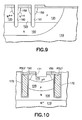
- Figure 9 shows the structure of Figure 8 after an emitter drive and trench etch.
- Figure 10 shows the structure of Figure 9 after the completion of the trench cell such as that in Figure 2.
- the structure of Figure 1 is formed in a common starting wafer 25 of float zone material.
- an epitaxial wafer can also be used.
- the wafer 25 has an N - body which receives adjacent deep trenches 31 and 32 which are lined with thin (for example 1000 ⁇ ) silicon dioxide gate insulation layers 33, 34 respectively and are filled with conductive polysilicon gates 35 and 36 respectively which are interconnected (not shown and have an external gate terminal G, schematically shown.
- Trenches 31 and 32 may be about 1.5 microns wide, spaced by about 5 to 10 microns and may have a depth of 4 to 9 microns, and preferably about 6.5 microns. These extend through a P- base diffusion 37 which, at the trench region, is about 5 microns deep (as measured from the top surface of the silicon) for an 8 micron deep trench.
- Trenches 31 and 32 extend through N + emitter regions 40 and 41 respectively which are very deep (2 microns to 4 microns) and have a very short lateral extension, for example 1.5 microns to 3 microns. Note that emitter regions 40 and 41 have shallow shelf contact regions 42 and 43 respectively, which have a lateral extension of about 0.2 microns to 0.5 microns.
- trenches 31 and 32 extend into the deep enhancement region 100 for about 2 ⁇ m (non-critical).
- a P + contact region 50 extends into P - base 37 and between emitter regions 40 and 41.
- the polysilicon gates 35 and 36 are covered by a suitable insulation oxide 51 and the top surface of the device receives an aluminum or other suitable emitter contact 52.
- the backside of the device contains a P + diffusion 54 which receives collector contact 53.
- the use of the very deep trench (6.5 microns) and very deep P - base 37 (7 microns) permits the use of the very deep, but narrow emitter regions 40 and 41 while still leaving a sufficiently long invertible channel below the emitter regions (for example, 2 microns) to permit the P regions 37 to support a reasonable voltage and so that the N - body 26 can be optimized.
- a hole current flows from P + region 54 and up and under the emitters 40 and 41 and through the effective resistance R B , under the emitter regions 40 and 41. This resistance is very low to avoid the turn on of the NPN transistor 40, 37, 26, for example, and to avoid latching on the IGBT structure.
- ledge regions 43, 43 of emitters 40 and 41 respectively are atop the P + regions 50 and do not form a part of the R B , of the device. These ledges 42, 43, however are major points for connection of the emitter regions 40 and 41 to emitter contact and permit such connection even with unavoidable mask misalignment during manufacture..
- the present invention is an improvement of the structure of Figure 1 and is shown in Figure 2, where components similar to those of Figure 1 are given the same identifying numerals.
- the basic difference in Figure 2 is the use of the novel deep enhancement N region 100 which is disposed between the bottoms of trenches 31 and 32 and beneath the trenches.
- the N region 100 would be a P region in a P channel device with all other concentration types reversed.
- the deep enhancement 100 may have a depth of 4 ⁇ m to 10 ⁇ m (with a 6 ⁇ m deep trench) and has a concentration substantially greater than that of N - body 26. This deep enhancement 100 reduces the spreading and drift region resistance of the device, thereby to reduce the forward voltage drop of the device. Further, the region 100 can be adjusted in concentration and depth to optimize the device to a specific application. For example, switching frequency can be preferred over other parameters for a particular application. In a high lifetime epitaxial device, the irradiation dose can be increased to reduce turn-off current at the switching time to reduce switching losses for the same forward voltage drop. Further, in a low lifetime depletion stop type trench IGBT, the deep enhancement region 100 will substantially reduce the forward voltage drop.
- Figures 3 to 9 show a process sequence which can be used to make the device of Figure 2.
- the doses and implant densities described are for a particular device and can be altered as desired while still practicing the present invention.
- a starting wafer 110 of silicon having a resistivity of 22 to 30 ohm-cm has an oxide layer 111 grown thereon to a thickness of 1 ⁇ m.
- Figure 4 shows a mask step in which a photoresist 112 is processed to open a window 113 in oxide layer 111.
- a phosphorus implant of dose between 1E12 to 1E13/cm 2 at 120 KeV is then applied to the exposed silicon surface in Figure 4.
- the photoresist 112 is then stripped and the phosphorus implant is driven for 4 to 16 hours at 1175°C to drive the novel deep N diffusion 100.
- oxide 111 grows to about 1.2 ⁇ m and thinner oxide layer 120 grows to about 7000 ⁇ as shown in Figure 5. Region 100 will deepen with each subsequent thermal treatment..
- a termination mask step is then carried out and, as shown in Figure 6, the termination mask defines windows in oxide layers 111 and 120 and the wafer is exposed to a boron implant at a dose of 7E14/cm 2 . This implant is then driven for 2 hours at 1175°C as shown in Figure 7, forming the P + channel region 125 and termination diffusion 126. At the same time new oxide is grown, including thickened regions 130 (9000 ⁇ ), 131 (1.4 ⁇ m) and 132 (7000 ⁇ ).
- FIG 8 shows the next step in which a trench mask 140 is provided which also acts as an emitter implant mask.
- windows 141 and 142 are opened in oxide 130, 132 and an arsenic implant is carried out at 1E16/cm 2 at 120 KeV.
- the implant is then driven for 30 minutes at 1175°C, forming N ++ emitter regions 150.
- a trench etch is carried out, forming spaced parallel trenches 160, 161 having a depth of about 6 ⁇ m.
- the cell structure is then completed as shown in U.S. Patent 6,683,331 and as shown in Figure 9. Note that the P + region 170 is implanted and diffused through contact window 171 which is about 3 ⁇ m wide.
- the gate oxide 172 is about 1500 ⁇ thick and the trench spacing is about 6 ⁇ m.
- the trench widths are about 1.5 microns.
- the cells described are two of up to many thousands in a single die, and are formed with the die in the wafer stage.
- die and wafer may herein be used interchangeably.
- An increased conductivity deep diffusion of the same conductivity type as that of the drift region is provided between adjacent trenches of a trench type IGBT and below the trenches to reduce the on resistance components of the drift region resistance and spreading resistance to current flow when the device is turned on.
- the deep diffusion has a higher concentration than that of the drift region, and has a width of from 4 to 10 microns.
- the wafer or die has a total width (or thickness) of about 70 to about 300 microns.
Landscapes
- Electrodes Of Semiconductors (AREA)
- Thyristors (AREA)
- Semiconductor Integrated Circuits (AREA)
Abstract
Description
- This invention relates to trench type Insulated Gate Bipolar Transistors (IGBTs) and more specifically relates to such IGBTs with a reduced forward voltage drop.
- IGBTs are well known and are frequently implemented with a planar cellular or stripe topology. These devices have an inherent JFET which increases the device on-resistance RDSON and, thus the forward voltage drop VCE(ON). Further, such devices have an inherent four layer parasitic thyristor structure which will latch on if the NPN transistor of the thyristor turns on.
- It is known that IGBTs can be made with a trench topology which eliminates the inherent JFET of the planar device. However, trench IGBTs still have the inherent four layer structure whereby, if the inherent NPN transistor in the four layer device turns on (if the current through RB, is sufficiently high), the device will latch on. It is also desirable to reduce the saturation current of the device without increasing the value of RB.
- It has further been found that trench IGBTs tend to be "fragile", that is, they can fail particularly when switching an inductive load. This is sometimes termed a low safe operating area (SOA) under reverse bias. This problem again is aggravated by an increased RB'.
-
U.S. Patent 6,683,331 the disclosure of which is incorporated herein by reference, describes a trench IGBT structure and process for its manufacture, creating a non-punch through (NPT) IGBT having a reduced RB', a reduced saturation current, a low threshold voltage VT and an enlarged SOA. More specifically, a structure is .provided having a deep emitter diffusion which is very narrow (of small lateral extent) to reduce RB'. Further, a very deep P channel diffusion is employed between spaced trenches to create a very long inversion channel. Thus, when the device goes into avalanche, the path for hole current under the emitter has a reduced lateral extent, reducing RB, and the trench is very deep (about 8 microns) so that the P region adjacent the channel can support reasonable voltage and the N- body concentration and depth can be optimized. The increased depth of the emitter along the trench controls threshold voltage since it permits the use of a very deep P+ region without the danger of its encroaching into the channel (which would increase VT). Finally, a helium implant may be employed for lifetime killing in only the P well. - Further, the device of the 6,683,331 patent may be built in float zone silicon and no epitaxial layer is needed, with a weak anode structure being employed as in copending application Serial No. 09/565,922, filed May 5, 2000 in the names of Richard Francis and Chiu Ng now
U.S. patent 6,482,681 . - In the trench IGBT structure disclosed in
US6,683,331 the current during forward conduction can be seen as a combination of MOSFET and bipolar currents. The specific on-resistance to the MOSFET current is determined by several components. In 300 - 1200V devices, due to the relatively high resistivity of the drift layer (typically 14-60 Ohm-cm) the major contribution of on resistance is from drift region resistance and spreading resistance below the channel region. - It would be very desirable to provide a device with the advantages of the device of patent 6,683,331, but with a reduced on-resistance.
- In accordance with the invention, the spreading and drift region resistance in a trench type IGBT is reduced by the introduction of a deep diffusion layer below the base diffusion. This deep diffusion or "Deep Enhancement", has an opposite doping concentration with respect to the P type base (or N type for an N channel device). The present invention reduces the device forward voltage drop by reducing on resistance. Further the invention provides the possibility to optimize the device to specific applications (e.g. switching frequency). Further, with the invention, in an high lifetime, epitaxial type trench IGBT, the irradiation dose can be increased to reduce the turn-off current and the switching time, hence reducing switching losses for the same forward drop. This is very useful in many applications, and significantly, in a low lifetime, depletion stop type trench IGBT, the deep enhancement of the invention will substantially reduce the device forward drop.
- Figure 1 is a cross-section through two adjacent trenches of an IGBT trench die having the junction pattern of the device of patent 6,683,331.
- Figure 2 is a cross-section like that of Figure 1, but showing the added novel deep enhancement of the invention.
- Figure 3 shows a small portion of a wafer (or die) in cross-section, showing a first step in the process to produce the device of Figure 2.
- Figure 4 shows the structure of Figure 3 after a mask and implant step.
- Figure 5 shows the structure of Figure 4 after a diffusion drive to form an N diffusion.
- Figure 6 shows the structure of Figure 5 after a termination mask step and termination implant.
- Figure 7 shows the structure of Figure 6 after a boron drive and oxidation step.
- Figure 8 shows the structure of Figure 7 after a trench mask and emitter implant.
- Figure 9 shows the structure of Figure 8 after an emitter drive and trench etch.
- Figure 10 shows the structure of Figure 9 after the completion of the trench cell such as that in Figure 2.
- Referring first to Figure 1 there is shown, in cross-section a pair of adjacent cells of the prior art structure of Patent 6,683,331.
- The detail of manufacture of the device of Figure 1 is disclosed in patent 6,683,331, including the materials used and process detail such as the reduction of the wafer thickness and the formation of the life time killing used and the
collector backside implant 54 and the like. - The structure of Figure 1 is formed in a common starting
wafer 25 of float zone material. However, an epitaxial wafer can also be used. Thewafer 25 has an N- body which receives adjacentdeep trenches gate insulation layers conductive polysilicon gates Trenches base diffusion 37 which, at the trench region, is about 5 microns deep (as measured from the top surface of the silicon) for an 8 micron deep trench. -
Trenches emitter regions shelf contact regions - Significantly,
trenches deep enhancement region 100 for about 2µm (non-critical). - A P+
contact region 50 extends into P- base 37 and betweenemitter regions polysilicon gates suitable insulation oxide 51 and the top surface of the device receives an aluminum or othersuitable emitter contact 52. The backside of the device contains a P+ diffusion 54 which receivescollector contact 53. - The use of the very deep trench (6.5 microns) and very deep P- base 37 (7 microns) permits the use of the very deep, but
narrow emitter regions P regions 37 to support a reasonable voltage and so that the N- body 26 can be optimized. Further, when the device operates in avalanche, a hole current flows from P+ region 54 and up and under theemitters emitter regions NPN transistor - Note that the
ledge regions emitters emitter regions - The present invention is an improvement of the structure of Figure 1 and is shown in Figure 2, where components similar to those of Figure 1 are given the same identifying numerals. The basic difference in Figure 2 is the use of the novel deep
enhancement N region 100 which is disposed between the bottoms oftrenches N region 100 would be a P region in a P channel device with all other concentration types reversed. - The
deep enhancement 100 may have a depth of 4µm to 10µm (with a 6µm deep trench) and has a concentration substantially greater than that of N- body 26. Thisdeep enhancement 100 reduces the spreading and drift region resistance of the device, thereby to reduce the forward voltage drop of the device. Further, theregion 100 can be adjusted in concentration and depth to optimize the device to a specific application. For example, switching frequency can be preferred over other parameters for a particular application. In a high lifetime epitaxial device, the irradiation dose can be increased to reduce turn-off current at the switching time to reduce switching losses for the same forward voltage drop. Further, in a low lifetime depletion stop type trench IGBT, thedeep enhancement region 100 will substantially reduce the forward voltage drop. - Figures 3 to 9 show a process sequence which can be used to make the device of Figure 2. The doses and implant densities described are for a particular device and can be altered as desired while still practicing the present invention. Thus, in Figure 3 a starting
wafer 110 of silicon having a resistivity of 22 to 30 ohm-cm has anoxide layer 111 grown thereon to a thickness of 1µm. - Figure 4 shows a mask step in which a
photoresist 112 is processed to open awindow 113 inoxide layer 111. A phosphorus implant of dose between 1E12 to 1E13/cm2 at 120 KeV is then applied to the exposed silicon surface in Figure 4. - The
photoresist 112 is then stripped and the phosphorus implant is driven for 4 to 16 hours at 1175°C to drive the noveldeep N diffusion 100. At the same time,oxide 111 grows to about 1.2µm andthinner oxide layer 120 grows to about 7000Å as shown in Figure 5.Region 100 will deepen with each subsequent thermal treatment.. - A termination mask step is then carried out and, as shown in Figure 6, the termination mask defines windows in
oxide layers termination diffusion 126. At the same time new oxide is grown, including thickened regions 130 (9000Å), 131 (1.4µm) and 132 (7000Å). - Figure 8 shows the next step in which a
trench mask 140 is provided which also acts as an emitter implant mask. Thus,windows oxide - Thereafter, as shown in Figure 8 a trench etch is carried out, forming spaced
parallel trenches - The cell structure is then completed as shown in
U.S. Patent 6,683,331 and as shown in Figure 9. Note that the P+ region 170 is implanted and diffused throughcontact window 171 which is about 3µm wide. Thegate oxide 172 is about 1500Å thick and the trench spacing is about 6µm. The trench widths are about 1.5 microns. - In the process described, the cells described are two of up to many thousands in a single die, and are formed with the die in the wafer stage. The terms die and wafer may herein be used interchangeably.
- Although the present invention has been described in relation to particular embodiments thereof, many other variations and modifications and other uses will become apparent to those skilled in the art. It is preferred, therefore, that the present invention be limited not by the specific disclosure herein.
An increased conductivity deep diffusion of the same conductivity type as that of the drift region is provided between adjacent trenches of a trench type IGBT and below the trenches to reduce the on resistance components of the drift region resistance and spreading resistance to current flow when the device is turned on. The deep diffusion has a higher concentration than that of the drift region, and has a width of from 4 to 10 microns. The wafer or die has a total width (or thickness) of about 70 to about 300 microns.
Claims (14)
- A trench IGBT having a deep diffusion for reducing its forward voltage drop, comprising a body of monocrystaline silicon of one of the conductivity types and having a first concentration, and having a parallel top and bottom surfaces; a plurality of spaced trenches extending perpendicularly into said top surface for a given depth; a gate insulation layer lining the vertical walls of said trenches; a channel diffusion of the other conductivity type formed between each of said trenches and having a depth which is less than the depth of said trenches; an emitter diffusion of said one of the conductivity types extending from said top surface of said body and along an upper portion of each of said trenches; said emitter diffusions being spaced from one another by a given distance between said trenches; a shallow contact diffusion of said other conductivity type which has a high concentration compared to that of said channel diffusion and disposed between adjacent pairs of said emitter diffusions; a collector diffusion of said other conductivity type in said bottom surface; an emitter metal electrode in contact with said emitter and channel diffusions and a collector electrode in contact with said collector diffusion; and a deep diffusion of said one conductivity type and having a conductivity greater than that of said first conductivity disposed beneath said channel diffusion and extending to beneath the bottom of said trenches.
- The device of claim 1, wherein said trenches have a depth of from 4 to 9 microns and are spaced by about 5 to 10 microns and have a width of about 1.5 microns.
- The device of claim 1, wherein said trenches have a depth of about 6 microns and wherein said trenches are deeper than said channel diffusion and said deep diffusion has a width of 4 to 10 microns.
- The device of claim 1, wherein the top surface of said emitter regions each have further high concentration shallow contact diffusions of said other of the conductivity types.
- The device of claim 2, wherein the top surface of said emitter regions each have further high concentration shallow contact diffusions of said other of the conductivity types.
- The device of claim 3, wherein the top surface of said emitter regions each have further high concentration shallow contact diffusions of said other of the conductivity types.
- The device of claim 1, wherein said emitter regions have a depth of 2 to 4 microns and a lateral width of 1.5 to 3 microns, and wherein said depth is greater than said width.
- The device of claim 1, wherein said emitter regions have shallow lateral extensions facing further away from their respective trenches to provide an increased contact surface to contact said emitter metal.
- The device of claim 8, wherein the top surface of said emitter regions each have further high concentration shallow diffusions of said other of the conductivity types.
- The device of claim 9, wherein said trenches have a depth of from 4 to 9 microns and are spaced by about 5 to 10 microns and have a width of about 1.5 microns.
- The device of claim 1, wherein said one conductivity type is N.
- The device of claim 1, wherein said trenches are laterally spaced straight parallel trenches.
- The device of claim 1, wherein said trenches are multi-sided polygons in cross-section through the depth of said trenches.
- The device of claim 1, which includes a further diffusion of a first conductivity type into said channel region and having a higher concentration than that of said channel region; said further diffusion extending under said lateral extensions of said emitter regions and making contact to said emitter metal.
Applications Claiming Priority (1)
| Application Number | Priority Date | Filing Date | Title |
|---|---|---|---|
| US11/204,074 US20070034941A1 (en) | 2005-08-15 | 2005-08-15 | Deep N diffusion for trench IGBT |
Publications (2)
| Publication Number | Publication Date |
|---|---|
| EP1755168A2 true EP1755168A2 (en) | 2007-02-21 |
| EP1755168A3 EP1755168A3 (en) | 2007-03-07 |
Family
ID=37501723
Family Applications (1)
| Application Number | Title | Priority Date | Filing Date |
|---|---|---|---|
| EP06016715A Withdrawn EP1755168A3 (en) | 2005-08-15 | 2006-08-10 | Deep N diffusion for trench IGBT |
Country Status (5)
| Country | Link |
|---|---|
| US (1) | US20070034941A1 (en) |
| EP (1) | EP1755168A3 (en) |
| JP (1) | JP2007053375A (en) |
| KR (1) | KR20080099834A (en) |
| CN (1) | CN1921146A (en) |
Cited By (3)
| Publication number | Priority date | Publication date | Assignee | Title |
|---|---|---|---|---|
| RU2585880C1 (en) * | 2015-05-14 | 2016-06-10 | Федеральное государственное автономное образовательное учреждение высшего образования "Национальный исследовательский технологический университет "МИСиС" | Integrated circuit of power bipolar-field-effect transistor |
| EP3514834A1 (en) * | 2018-01-23 | 2019-07-24 | Infineon Technologies Austria AG | Semiconductor device having body contacts with dielectric spacers and corresponding methods of manufacture |
| US10720500B2 (en) | 2016-08-01 | 2020-07-21 | Infineon Technologies Austria Ag | Transistor device with a field electrode that includes two layers |
Families Citing this family (14)
| Publication number | Priority date | Publication date | Assignee | Title |
|---|---|---|---|---|
| CN100592532C (en) * | 2007-08-28 | 2010-02-24 | 电子科技大学 | Semiconductor device with "U"-shaped drift region |
| US8441046B2 (en) * | 2010-10-31 | 2013-05-14 | Alpha And Omega Semiconductor Incorporated | Topside structures for an insulated gate bipolar transistor (IGBT) device to achieve improved device performances |
| CN102074575B (en) * | 2010-11-15 | 2013-09-11 | 嘉兴斯达半导体股份有限公司 | IGBT (Insulated Gate Bipolar Translator) device structure and preparation method thereof |
| CN102169892B (en) * | 2011-03-09 | 2012-11-07 | 电子科技大学 | Enhancement mode planar insulated gate bipolar transistor (IGBT) |
| CN102184949B (en) * | 2011-05-09 | 2012-09-12 | 电子科技大学 | Deep groove side oxygen controlled planar isolated gate bipolar transistor |
| CN103022113B (en) * | 2011-09-20 | 2016-04-13 | 上海华虹宏力半导体制造有限公司 | A kind of igbt structure and manufacture method thereof |
| US9525057B2 (en) | 2012-05-15 | 2016-12-20 | Mitsubishi Electric Corporation | Semiconductor device |
| CN103872114A (en) * | 2012-12-13 | 2014-06-18 | 中国科学院微电子研究所 | Groove type IGBT and manufacturing method thereof |
| US9768284B2 (en) | 2015-03-05 | 2017-09-19 | Infineon Technologies Americas Corp. | Bipolar semiconductor device having a charge-balanced inter-trench structure |
| US9831330B2 (en) * | 2015-03-05 | 2017-11-28 | Infineon Technologies Americas Corp. | Bipolar semiconductor device having a deep charge-balanced structure |
| US9685506B2 (en) * | 2015-03-05 | 2017-06-20 | Infineon Technologies Americas Corp. | IGBT having an inter-trench superjunction structure |
| CN108122971B (en) * | 2017-12-25 | 2020-11-27 | 电子科技大学 | A kind of RC-IGBT device and preparation method thereof |
| JP7294568B2 (en) * | 2019-03-20 | 2023-06-20 | 日本カーバイド工業株式会社 | Adhesive composition for heat-resistant adhesive sheet, heat-resistant adhesive sheet, and laminate |
| CN110504313B (en) * | 2019-08-29 | 2023-02-03 | 电子科技大学 | A lateral trench type insulated gate bipolar transistor and its preparation method |
Citations (2)
| Publication number | Priority date | Publication date | Assignee | Title |
|---|---|---|---|---|
| US6482681B1 (en) | 2000-05-05 | 2002-11-19 | International Rectifier Corporation | Hydrogen implant for buffer zone of punch-through non epi IGBT |
| US6683331B2 (en) | 2002-04-25 | 2004-01-27 | International Rectifier Corporation | Trench IGBT |
Family Cites Families (9)
| Publication number | Priority date | Publication date | Assignee | Title |
|---|---|---|---|---|
| JP3288218B2 (en) * | 1995-03-14 | 2002-06-04 | 三菱電機株式会社 | Insulated gate semiconductor device and method of manufacturing the same |
| US6768168B1 (en) * | 1995-03-14 | 2004-07-27 | Mitsubishi Denki Kabushiki Kaisha | Insulated gate semiconductor device with low on voltage and manufacturing method thereof |
| US6040599A (en) * | 1996-03-12 | 2000-03-21 | Mitsubishi Denki Kabushiki Kaisha | Insulated trench semiconductor device with particular layer structure |
| JP3764343B2 (en) * | 2001-02-28 | 2006-04-05 | 株式会社東芝 | Manufacturing method of semiconductor device |
| JP3973934B2 (en) * | 2002-03-15 | 2007-09-12 | 株式会社東芝 | High voltage semiconductor device |
| JP2004022941A (en) * | 2002-06-19 | 2004-01-22 | Toshiba Corp | Semiconductor device |
| JP4133548B2 (en) * | 2003-04-25 | 2008-08-13 | 新電元工業株式会社 | Semiconductor device |
| JP4538211B2 (en) * | 2003-10-08 | 2010-09-08 | トヨタ自動車株式会社 | Insulated gate semiconductor device and manufacturing method thereof |
| KR100767078B1 (en) * | 2003-10-08 | 2007-10-15 | 도요다 지도샤 가부시끼가이샤 | Insulated gate type semiconductor device and manufacturing method thereof |
-
2005
- 2005-08-15 US US11/204,074 patent/US20070034941A1/en not_active Abandoned
-
2006
- 2006-08-10 EP EP06016715A patent/EP1755168A3/en not_active Withdrawn
- 2006-08-15 JP JP2006221345A patent/JP2007053375A/en active Pending
- 2006-08-15 CN CNA2006101534285A patent/CN1921146A/en active Pending
-
2008
- 2008-09-18 KR KR1020080091803A patent/KR20080099834A/en not_active Withdrawn
Patent Citations (2)
| Publication number | Priority date | Publication date | Assignee | Title |
|---|---|---|---|---|
| US6482681B1 (en) | 2000-05-05 | 2002-11-19 | International Rectifier Corporation | Hydrogen implant for buffer zone of punch-through non epi IGBT |
| US6683331B2 (en) | 2002-04-25 | 2004-01-27 | International Rectifier Corporation | Trench IGBT |
Cited By (6)
| Publication number | Priority date | Publication date | Assignee | Title |
|---|---|---|---|---|
| RU2585880C1 (en) * | 2015-05-14 | 2016-06-10 | Федеральное государственное автономное образовательное учреждение высшего образования "Национальный исследовательский технологический университет "МИСиС" | Integrated circuit of power bipolar-field-effect transistor |
| US10720500B2 (en) | 2016-08-01 | 2020-07-21 | Infineon Technologies Austria Ag | Transistor device with a field electrode that includes two layers |
| US10957771B2 (en) | 2016-08-01 | 2021-03-23 | Infineon Technologies Austria Ag | Transistor device with a field electrode that includes two layers |
| US11581409B2 (en) | 2016-08-01 | 2023-02-14 | Infineon Technologies Austria Ag | Transistor device with a field electrode that includes two layers |
| EP3514834A1 (en) * | 2018-01-23 | 2019-07-24 | Infineon Technologies Austria AG | Semiconductor device having body contacts with dielectric spacers and corresponding methods of manufacture |
| US11031478B2 (en) | 2018-01-23 | 2021-06-08 | Infineon Technologies Austria Ag | Semiconductor device having body contacts with dielectric spacers and corresponding methods of manufacture |
Also Published As
| Publication number | Publication date |
|---|---|
| US20070034941A1 (en) | 2007-02-15 |
| JP2007053375A (en) | 2007-03-01 |
| KR20080099834A (en) | 2008-11-13 |
| EP1755168A3 (en) | 2007-03-07 |
| CN1921146A (en) | 2007-02-28 |
Similar Documents
| Publication | Publication Date | Title |
|---|---|---|
| JP7182594B2 (en) | Power semiconductor device with gate trench and buried termination structure and related method | |
| KR100305978B1 (en) | Field-effect trench transistors with lightly doped epitaxial regions on the surface of transistors | |
| US10763351B2 (en) | Vertical trench DMOSFET having integrated implants forming enhancement diodes in parallel with the body diode | |
| KR100952389B1 (en) | Power semiconductor device and method of forming the same device | |
| US6825105B2 (en) | Manufacture of semiconductor devices with Schottky barriers | |
| JP3938964B2 (en) | High voltage semiconductor device and manufacturing method thereof | |
| US7880200B2 (en) | Semiconductor device including a free wheeling diode | |
| US7161208B2 (en) | Trench mosfet with field relief feature | |
| KR20080099834A (en) | Deep N Diffusion for Trench ITV | |
| TW200305970A (en) | Power semiconductor device having a voltage sustaining region that includes doped columns formed with a single ion implantation step | |
| US11699744B2 (en) | Semiconductor device and semiconductor apparatus | |
| US7994569B2 (en) | Semiconductor device and method for forming the same | |
| KR20020077659A (en) | A semiconductor device for electric power | |
| JP2011103482A (en) | Method of fabricating silicon carbide power device by controlled annealing | |
| EP0869558A2 (en) | Insulated gate bipolar transistor with reduced electric fields | |
| US6683331B2 (en) | Trench IGBT | |
| JP2005510061A (en) | Trench gate semiconductor device and manufacturing method thereof | |
| CN113517332A (en) | Complex superjunction semiconductor device based on cylindrical superjunction region and its fabrication method | |
| US20070063269A1 (en) | Trench IGBT with increased short circuit capability | |
| CN114597264A (en) | A power MOSFET device and method of making the same | |
| CN110504313A (en) | A lateral trench type insulated gate bipolar transistor and its preparation method | |
| CN114388612A (en) | Semiconductor device and method for manufacturing semiconductor device | |
| US20250081491A1 (en) | Trench-gated switch with epitaxial p-body layer having higher doped top portion | |
| KR19980037074A (en) | Insulated Gate Bipolar Transistor | |
| KR20070020358A (en) | Deep N diffusion for trench ITV |
Legal Events
| Date | Code | Title | Description |
|---|---|---|---|
| PUAI | Public reference made under article 153(3) epc to a published international application that has entered the european phase |
Free format text: ORIGINAL CODE: 0009012 |
|
| PUAL | Search report despatched |
Free format text: ORIGINAL CODE: 0009013 |
|
| 17P | Request for examination filed |
Effective date: 20060810 |
|
| AK | Designated contracting states |
Kind code of ref document: A2 Designated state(s): AT BE BG CH CY CZ DE DK EE ES FI FR GB GR HU IE IS IT LI LT LU LV MC NL PL PT RO SE SI SK TR |
|
| AX | Request for extension of the european patent |
Extension state: AL BA HR MK YU |
|
| AK | Designated contracting states |
Kind code of ref document: A3 Designated state(s): AT BE BG CH CY CZ DE DK EE ES FI FR GB GR HU IE IS IT LI LT LU LV MC NL PL PT RO SE SI SK TR |
|
| AX | Request for extension of the european patent |
Extension state: AL BA HR MK YU |
|
| AKX | Designation fees paid |
Designated state(s): AT BE BG CH CY CZ DE DK EE ES FI FR GB GR HU IE IS IT LI LT LU LV MC NL PL PT RO SE SI SK TR |
|
| 17Q | First examination report despatched |
Effective date: 20101223 |
|
| STAA | Information on the status of an ep patent application or granted ep patent |
Free format text: STATUS: THE APPLICATION HAS BEEN WITHDRAWN |
|
| 18W | Application withdrawn |
Effective date: 20130911 |