EP1755166A2 - Solid-state imaging device - Google Patents
Solid-state imaging device Download PDFInfo
- Publication number
- EP1755166A2 EP1755166A2 EP06023938A EP06023938A EP1755166A2 EP 1755166 A2 EP1755166 A2 EP 1755166A2 EP 06023938 A EP06023938 A EP 06023938A EP 06023938 A EP06023938 A EP 06023938A EP 1755166 A2 EP1755166 A2 EP 1755166A2
- Authority
- EP
- European Patent Office
- Prior art keywords
- charge
- gate
- drain
- state imaging
- imaging device
- Prior art date
- Legal status (The legal status is an assumption and is not a legal conclusion. Google has not performed a legal analysis and makes no representation as to the accuracy of the status listed.)
- Withdrawn
Links
Images




Classifications
-
- H—ELECTRICITY
- H04—ELECTRIC COMMUNICATION TECHNIQUE
- H04N—PICTORIAL COMMUNICATION, e.g. TELEVISION
- H04N25/00—Circuitry of solid-state image sensors [SSIS]; Control thereof
- H04N25/70—SSIS architectures; Circuits associated therewith
- H04N25/71—Charge-coupled device [CCD] sensors; Charge-transfer registers specially adapted for CCD sensors
- H04N25/75—Circuitry for providing, modifying or processing image signals from the pixel array
-
- H—ELECTRICITY
- H10—SEMICONDUCTOR DEVICES; ELECTRIC SOLID-STATE DEVICES NOT OTHERWISE PROVIDED FOR
- H10F—INORGANIC SEMICONDUCTOR DEVICES SENSITIVE TO INFRARED RADIATION, LIGHT, ELECTROMAGNETIC RADIATION OF SHORTER WAVELENGTH OR CORPUSCULAR RADIATION
- H10F39/00—Integrated devices, or assemblies of multiple devices, comprising at least one element covered by group H10F30/00, e.g. radiation detectors comprising photodiode arrays
- H10F39/10—Integrated devices
- H10F39/12—Image sensors
- H10F39/15—Charge-coupled device [CCD] image sensors
- H10F39/151—Geometry or disposition of pixel elements, address lines or gate electrodes
-
- H—ELECTRICITY
- H10—SEMICONDUCTOR DEVICES; ELECTRIC SOLID-STATE DEVICES NOT OTHERWISE PROVIDED FOR
- H10F—INORGANIC SEMICONDUCTOR DEVICES SENSITIVE TO INFRARED RADIATION, LIGHT, ELECTROMAGNETIC RADIATION OF SHORTER WAVELENGTH OR CORPUSCULAR RADIATION
- H10F39/00—Integrated devices, or assemblies of multiple devices, comprising at least one element covered by group H10F30/00, e.g. radiation detectors comprising photodiode arrays
- H10F39/80—Constructional details of image sensors
- H10F39/802—Geometry or disposition of elements in pixels, e.g. address-lines or gate electrodes
-
- H—ELECTRICITY
- H10—SEMICONDUCTOR DEVICES; ELECTRIC SOLID-STATE DEVICES NOT OTHERWISE PROVIDED FOR
- H10D—INORGANIC ELECTRIC SEMICONDUCTOR DEVICES
- H10D44/00—Charge transfer devices
- H10D44/40—Charge-coupled devices [CCD]
- H10D44/45—Charge-coupled devices [CCD] having field effect produced by insulated gate electrodes
- H10D44/454—Output structures
-
- H—ELECTRICITY
- H10—SEMICONDUCTOR DEVICES; ELECTRIC SOLID-STATE DEVICES NOT OTHERWISE PROVIDED FOR
- H10F—INORGANIC SEMICONDUCTOR DEVICES SENSITIVE TO INFRARED RADIATION, LIGHT, ELECTROMAGNETIC RADIATION OF SHORTER WAVELENGTH OR CORPUSCULAR RADIATION
- H10F39/00—Integrated devices, or assemblies of multiple devices, comprising at least one element covered by group H10F30/00, e.g. radiation detectors comprising photodiode arrays
- H10F39/80—Constructional details of image sensors
- H10F39/803—Pixels having integrated switching, control, storage or amplification elements
Definitions
- the present invention relates to solid-state imaging devices.
- Fig. 1 is a plan view illustrating an example of a known solid-state imaging device.
- a solid-state imaging device 102 shown in Fig. 1 a plurality of photoelectric conversion elements 106 are disposed in a matrix with a gap therebetween on a photodetector region 105 of a silicon semiconductor substrate 104.
- a vertical charge transfer register 108 having a charge coupled device (CCD) structure is disposed for each column of the photoelectric conversion elements 106 in the vertical direction (indicated by the arrow V in Fig. 1 of the photoelectric conversion elements 106.
- a horizontal charge transfer register 110 also having a CCD structure is disposed at one side of the individual vertical charge transfer registers 108 in the horizontal direction (indicated by the arrow H in Fig. 1) of the photoelectric conversion elements 106.
- An output portion 112 is formed at one end of the horizontal charge transfer register 110.
- the vertical charge transfer register 108 sequentially transfers the signal charges to the horizontal charge transfer register 110.
- the horizontal charge transfer register 110 transfers the signal charges to the output portion 112.
- the output portion 112 converts the signal charges into a voltage signal, amplifies it, and outputs the amplified signal.
- the number of pixels should be increased. To achieve this, it is necessary to dispose more photoelectric conversion elements 106 on the semiconductor substrate 104. However, an increased number of photoelectric conversion elements 106 prolongs the time required for transferring the signal charge, and it becomes difficult to ensure the sufficient frame frequency required for displaying captured images.
- a solid-state imaging device in which the photoelectric conversion elements 106 are divided into two groups, which then transfer signal charges by using two horizontal charge transfer registers.
- Fig. 2 is a schematic diagram illustrating such a solid-state imaging device.
- a photodetector region 105 on a semiconductor substrate is divided into first and second photodetector areas 116 and 118, and a plurality of photoelectric conversion elements disposed in a matrix are divided into a group disposed in the first photodetector area 116 and a group disposed on the second photodetector area 118.
- the signal charges generated by the photoelectric conversion elements in the first and second photodetector areas 116 and 118 are respectively transferred to first and second horizontal charge transfer registers 120 and 122 by using the corresponding vertical charge transfer registers.
- the photoelectric conversion elements and the vertical charge transfer registers are not shown in Fig. 2.
- the first and second horizontal charge transfer registers 120 and 122 Upon receiving the signal charges from the vertical charge transfer registers, the first and second horizontal charge transfer registers 120 and 122 simultaneously transfer the signal charges in the opposite directions so as to supply them to first and second output portions 124 and 126, respectively, formed at the corresponding ends of the first and second horizontal charge transfer registers 120 and 122. Then, signals indicating images captured by the photoelectric conversion elements disposed in the first and second photodetector areas 116 and 118 are simultaneously output from the first and second output portions 124 and 126, respectively. Accordingly, in the solid-state imaging device 114, the time required for transferring the signal charge is decreased to one half the time for a solid-state imaging device using only one horizontal charge transfer register.
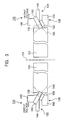
- Fig. 3 is a plan view illustrating details of the first and second output portions 124 and 126 disposed at the corresponding ends of the first and second horizontal charge transfer registers 120 and 122, respectively, shown in Fig. 2.
- the first and second output portions 124 and 126 respectively include first and second signal charge detectors 128 and 130, first and second transistors 132 and 134, and first and second charge sweeping regions 136 and 138.
- Each of the first and second horizontal charge transfer registers 120 and 122 includes a transfer passage 140, which is, for example, an n-type region formed on the surface of a p-type semiconductor substrate, and transfer electrodes (not shown) disposed on the transfer passage 140 in the charge transfer direction.
- the transfer passage 140 is formed to be narrower, as shown in Fig. 3, as it goes to the end of each of the first and second horizontal charge transfer registers 120 and 122.
- Each of the first and second signal charge detectors 128 and 130 is formed as, for example, an n-type region on the surface of the semiconductor substrate, at the vicinity of the front end of the transfer passage 140.
- Each of the first and second transistors 132 and 134 includes a gate 142, a source 144, and a drain 146.
- the gate 142 is formed of, for example, polysilicon, and is formed such that one end thereof overlaps with the corresponding signal charge detector 128 or 130. In this example shown in Fig. 3, the gate 142 of the first transistor 132 extends upward toward the upper left side, while the gate 142 of the second transistor 134 extends upward toward the upper right side.
- the source 144 and the drain 146 of each of the first and second transistors 132 and 134 are formed as, for example, n-type regions on the surface of the semiconductor substrate, across the gate 142.
- Each of the first and second charge sweeping regions 136 and 138 includes, as shown in Fig. 3, a charge sweeping drain 150 and a charge sweeping control gate 152.
- the charge sweeping control gate 152 is disposed adjacent to the gate 142 of each of the first and second transistors 132 and 134, and the charge sweeping drain 150 is formed as, for example, an n-type region on the surface of the semiconductor, at a position opposite to the gate 142 across the charge sweeping control gate 152.
- the first signal charge detector 128, the first transistor 132, and the first charge sweeping region 136 are symmetrical to the second signal charge detector 130, the second transistor 134, and the second charge sweeping region 138, respectively, with respect to an imaginary line 154 drawn orthogonally to the direction in which the first and second horizontal charge transfer registers 120 and 122 are extended.
- signal charges transferred from the first and second horizontal charge transfer registers 120 and 122 are converted into voltage signals having a magnitude according to the amount of charge by the first and second signal charge detectors 128 and 130, and the first and second transistors 132 and 134 amplify the voltage signals and output them from the drains 146.
- the charge sweeping control gates 152 are controlled to be ON or OFF in synchronization with the charge transfer operation of the first and second horizontal charge transfer registers 120 and 122, and signal charges which have become unnecessary in the first and second signal charge detectors 128 and 130 are transferred to the charge sweeping drains 150 via the charge sweeping control gates 152.
- the first and second transistors 132 and 134 and the first and second sweeping regions 136 and 138 which form the first and second output portions 124 and 126, respectively, are formed on a semiconductor substrate according to a known semiconductor processing technique, which has a plurality of steps. During the processing, a plurality of masks, such as photoresist or silicon nitride film, are formed in each step according to, for example, a photolithographic technique. As a result, the sources 144, the drains 146, and the gates 142 are formed in predetermined configurations at predetermined positions on the semiconductor substrate.
- a photoresist film on a semiconductor substrate is exposed via a reticle, and is then developed so as to be formed into a mask pattern.
- the mask formed as described above is slightly displaced vertically, horizontally, to the left side, or to the right side from a correct position, on the mask surface within a predetermined allowance.
- the gate 142 of the first or second transistor 132 or 134 is slightly displaced with respect to a mask for forming the source 144 and a mask for forming the drain 146 of the corresponding transistor 132 or 134, the gate 142 is displaced from the correct position with respect to the source 144 and the drain 146.
- Such a displacement of the gate 142 adversely influences the characteristics of the corresponding transistor 132 or 134, which changes, for example, the degree of amplification of the transistor.
- Figs. 4A and 4B are partial plan views illustrating the gates 142 of the first and second transistors 132 and 134, respectively, which are formed slightly rightward from the correct positions due to displacements of the corresponding masks.
- the gate 142 of the first transistor 132 is also formed rightward.
- the area of the drain 146 of the first transistor 132 is smaller than it should be, while the area of the source 144 is larger than it should be.
- Such displacements of the masks from the correct positions change the characteristics of the first and second transistors 132 and 134 in different manners. For example, if the degree of amplification of one transistor is increased, the degree of amplification of the other transistor is decreased.
- the degree of amplification is different between the first and second transistors 132 and 134, the levels of the signals output from the first and second transistors 132 and 134 also become different. As a result, when captured images are displayed based on these signals, the brightness or the contrast becomes different between the left side and the right side of the screen.
- first and second signal charge detectors 128 and 130 and the first and second charge sweeping regions 136 and 138.
- the levels of the signals output from the first and second output portions 124 and 126 become different.
- a solid-state imaging device including: a plurality of photoelectric conversion elements; first and second charge transfer registers for transferring signal charges generated by the plurality of photoelectric conversion elements; first and second signal charge detectors, each being disposed in the vicinity of one edge of each of the first and second charge transfer registers, respectively; and first and second transistors.
- the above-described components are disposed on a semiconductor substrate.
- the first and second charge transfer registers transfer the signal charges in opposite directions.
- the first and second signal charge detectors receive the signal charges from the first and second charge transfer registers, respectively, and output voltages having a magnitude in accordance with the amount of charge.
- Each of the first and second transistors includes a gate into which the voltage output from the first or second signal charge detector is input, a source, and a drain, both of which are formed adjacent to the gate.
- the first signal charge detector, the source, the drain, and the gate of the first transistor are almost congruent to the second signal charge detector, the source, the drain, and the gate of the second transistor, respectively, when viewed from above.
- the first signal charge detector, the source, the drain, and the gate of the first transistor are overlaid almost completely on the second signal charge detector, the source, the drain, and the gate of the second transistor, respectively, by a translational movement.
- Fig. 5 is a partial plan view illustrating the essential portion of a solid-state imaging device 6 according to an embodiment of the present invention.
- the configuration of the solid-state imaging device 6 is similar to that of the solid-state imaging device 114 shown in Fig. 2 in the arrangement of the photoelectric conversion elements and charge transfer registers. That is, in the solid-state imaging device 6, a plurality of photoelectric conversion elements are formed in a matrix with a gap therebetween on a silicon semiconductor substrate 12.
- a vertical charge transfer register is provided for each column of the photoelectric conversion elements in the vertical direction of the photoelectric conversion elements, and horizontal charge transfer registers are disposed at one end of the individual vertical charge transfer registers.
- the photodetector region in which the photoelectric conversion elements are disposed are formed of first and second photodetector areas, and the horizontal charge transfer registers are formed of first and second horizontal charge transfer registers 8 and 10 provided for the first and second photodetector areas, respectively.
- the horizontal charge transfer registers 8 and 10 receive signal charges generated by the photoelectric conversion elements (first and second groups of photoelectric conversion elements) via the corresponding vertical charge transfer registers disposed in the first and second photodetector areas, and transfer the signal charges to corresponding first and second output portions 2 and 4.
- the solid-state imaging device 6 is different from a known solid-state imaging device in the configuration of the first and second output portions 2 and 4.
- Fig. 5 illustrates details of the first and second output portions 2 and 4 and the components disposed around them.
- the solid-state imaging device 6 includes the first and second horizontal charge transfer registers 8 and 10, which are disposed on the same imaginary line on the semiconductor substrate 12 such that signal charges are transferred in parallel to the imaginary line, and that one end of the first horizontal charge transfer register 8 opposedly faces one end of the second horizontal charge transfer register 10 (such opposing ends of the first and second horizontal charge transfer registers 8 and 10 are indicated by 14).
- the first and second output portions 2 and 4 are formed at the ends opposite to the opposing ends 14 of the first and second horizontal charge transfer registers 8 and 10, respectively.
- the first and second output portions 2 and 4 include first and second signal charge detectors 16 and 18, first and second transistors 20 and 22, and first and second charge sweeping regions 24 and 25, respectively.
- the signal charges are supplied to the first and second horizontal charge transfer registers 8 and 10 via the corresponding vertical charge transfer registers (not shown), and are then transferred in the opposite directions, i.e., toward the first and second output portions 2 and 4.
- Each of the first and second horizontal charge transfer registers 8 and 10 includes a transfer passage 26, which is, for example, an n-type region formed on the surface of the p-type semiconductor substrate 12, and a plurality of transfer electrodes (not shown) disposed on the transfer passage 26 in the charge transfer direction.
- the transfer passage 26 is, as shown in Fig. 5, formed in a configuration such that the end thereof close to each of the first and second signal charge detectors 16 and 18 is formed obliquely across the charge transfer direction when viewed from above.
- the first and second signal charge detectors 16 and 18 are formed adjacent to front ends 28 of the first and second horizontal charge transfer registers 8 and 10, respectively.
- the first and second signal charge detectors 16 and 18 are formed as n-type regions on the surface of the semiconductor substrate 12.
- the first and second transistors 20 and 22 forming the first and second output portions 2 and 4, respectively, are MOS transistors, and each includes a gate 30, a source 32, and a drain 34.
- the gates 30 of the first and second transistors 20 and 22 are formed of, for example, polysilicon, and are disposed so that one end of each gate 30 overlaps with the first and second signal charge detector 16 or 18.
- the gates 30 of the first and second transistors 20 and 22 extend downward toward the bottom right with the same tilting angle, and the configuration of the gate 30 of the first transistor 20 is almost congruent to that of the second transistor 22 when viewed from above. Accordingly, if the gate 30 of the first transistor 20 is translationally moved toward the gate 30 of the second transistor 22, it almost coincides with the gate 30 of the second transistor 22.
- the source 32 and the drain 34 are formed across the gate 30 as, for example, an n-type region on the surface of the semiconductor substrate 12.
- the configurations of the source 32 and the drain 34 of the first transistor 20 are almost congruent to those of the second transistor 22 when viewed from above. Accordingly, the source 32 and the drain 34 of the first transistor 20 are overlaid almost completely on those of the second transistor 22 by a translational movement.
- Each of the first and second charge sweeping regions 24 and 25 includes, as shown in Fig. 5, a charge sweeping drain 38 and a charge sweeping control gate 40, which is formed of, for example, polysilicon.
- the charge sweeping control gate 40 is disposed adjacent to the gate 30 of each of the first and second transistors 20 and 22.
- the charge sweeping drain 38 is formed as, for example, an n-type region on the surface of the semiconductor substrate 12, at a position opposite to the gate 30 across the charge sweeping control gate 40.
- the charge sweeping control gate 40 and the charge sweeping drain 38 of the first charge sweeping region 24 are almost congruent to those of the second charge sweeping region 25 when viewed from above. Accordingly, the charge sweeping control gate 40 and the charge sweeping drain 38 of the first charge sweeping region 24 are overlaid almost completely on those of the second charge sweeping region 25 by a translational movement.
- signal charges transferred from the first and second horizontal charge transfer registers 8 and 10 are converted into voltage signals having a magnitude according to the amount of charge by the first and second signal charge detectors 16 and 18, respectively, and the first and second transistors 20 and 22 amplify the voltage signals and output them from the corresponding drains 34.
- the charge sweeping control gates 40 are controlled to be ON or OFF in synchronization with the charge transfer operation of the first and second horizontal charge transfer registers 8 and 10, and signal charges which have become unnecessary in the first and second signal charge detectors 16 and 18 are transferred to the charge sweeping drains 38 via the charge sweeping control gates 40.
- the first signal charge detector 16, the source 32, the drain 34, and the gate 30 of the first transistor 20, and the first charge sweeping region 24 are almost congruent to the second charge detector 18, the source 32, the drain 34, and the gate 30 of the second transistor 22, and the second charge sweeping region 25. Additionally, the first signal charge detector 16, the source 32, the drain 34, and the gate 30 of the first transistor 20, and the first charge sweeping region 24 are overlaid almost completely on the second charge detector 18, the source 32, the drain 34, and the gate 30 of the second transistor 22, and the second charge sweeping region 25 by a translational movement. Thus, even if a mask for forming the above-described component is slightly displaced from the correct position, the levels of the signals output from the first and second transistors 20 and 22 do not become different.
- the positions and configurations of the sources 32 and the drains 34 of the first and second transistors 20 and 22 are determined by the positions and configurations of the components formed around the sources 32 and the drains 34, for example, field oxide film.
- the gate 30 is fabricated by forming a mask with the use of photoresist which will be opened at the corresponding position of the gate 30 and by depositing polysilicon in the opened portion. If the mask for forming the gate 30 is slightly displaced with respect to the mask for forming the field oxide film, the gate 30 is slightly displaced from the correct position with respect to the source 32 and the drain 34.
- the mask 30 is displaced, for example, slightly rightward in Fig. 5, the area of the drain 34 is smaller than it should be, and the area of the source 32 is larger than it should be.
- the gate 30, the source 32, and the drain 34 of the first transistor 20 are formed almost congruent to those of the second transistor 22, and since the above-described elements of the first transistor 20 are overlaid almost completely on the corresponding elements of the second transistor 22 by a translational movement, the amount by which the drain 34 is decreased due to a displacement of the gate 30 is almost the same between the first and second transistors 20 and 22, and an amount by which the source 32 is increased is almost the same between the first and second transistors 20 and 22.
- the characteristics of the first and second transistors 20 and 22 change due to a displacement of the gates 30, they change in a similar manner. Thus, there is no difference between the levels of the signals output from the first and second transistors 20 and 22.
- first and second signal charge detectors 16 and 18 and the first and second charge sweeping regions 24 and 25 Since the first signal charge detector 16 and the first charge sweeping region 24 are formed almost congruent to the second signal charge detector 18 and the second charge sweeping region 25, and since the first signal charge detector 16 the first charge sweeping region 24 are overlaid almost completely on the second signal charge detector 18 and the second charge sweeping region 25 by a translational movement, there is no difference in the electrical characteristics even if a mask is displaced during the manufacturing process, and thus, the level of the output signal from the first output portion 2 is not different from that from the second output portion 4.
- the first and second output portions 2 and 4 are formed under the first and second horizontal charge transfer registers 8 and 10, respectively.
- the first and second output portions 2 and 4 may be disposed at any position as long as the components of the output portions 2 and 4 are formed almost congruent with each other and they are overlaid almost completely on each other by a translational movement, in which case, advantages similar to those achieved by this embodiment can be obtained.
- the photoelectric conversion elements are disposed in a matrix, they may be linearly disposed, as in a linear image sensor, in which case, signal charge generated by the photoelectric conversion elements are transferred by two or more charge transfer registers.
Landscapes
- Engineering & Computer Science (AREA)
- Multimedia (AREA)
- Signal Processing (AREA)
- Solid State Image Pick-Up Elements (AREA)
- Transforming Light Signals Into Electric Signals (AREA)
- Light Receiving Elements (AREA)
Abstract
Description
- The present invention relates to solid-state imaging devices.
- Fig. 1 is a plan view illustrating an example of a known solid-state imaging device. In a solid-
state imaging device 102 shown in Fig. 1, a plurality ofphotoelectric conversion elements 106 are disposed in a matrix with a gap therebetween on aphotodetector region 105 of asilicon semiconductor substrate 104. A verticalcharge transfer register 108 having a charge coupled device (CCD) structure is disposed for each column of thephotoelectric conversion elements 106 in the vertical direction (indicated by the arrow V in Fig. 1 of thephotoelectric conversion elements 106. A horizontalcharge transfer register 110 also having a CCD structure is disposed at one side of the individual vertical charge transfer registers 108 in the horizontal direction (indicated by the arrow H in Fig. 1) of thephotoelectric conversion elements 106. Anoutput portion 112 is formed at one end of the horizontalcharge transfer register 110. - In the above-configured solid-
state imaging device 102, upon receiving light, signal charges are generated by each column of thephotoelectric conversion elements 106, and are supplied to the corresponding verticalcharge transfer register 108 via a read area (not shown) which intervenes between thephotoelectric conversion elements 106 and each of the vertical charge transfer registers 108. Then, the vertical charge transfer register 108 sequentially transfers the signal charges to the horizontalcharge transfer register 110. Upon receiving the signal charges from the individual vertical charge transfer registers 108, the horizontalcharge transfer register 110 then transfers the signal charges to theoutput portion 112. Theoutput portion 112 converts the signal charges into a voltage signal, amplifies it, and outputs the amplified signal. - In the solid-
state imaging device 102, in order to obtain a higher level of resolution of captured images, the number of pixels should be increased. To achieve this, it is necessary to dispose morephotoelectric conversion elements 106 on thesemiconductor substrate 104. However, an increased number ofphotoelectric conversion elements 106 prolongs the time required for transferring the signal charge, and it becomes difficult to ensure the sufficient frame frequency required for displaying captured images. - In order to overcome the above-described drawback, a solid-state imaging device has been proposed in which the
photoelectric conversion elements 106 are divided into two groups, which then transfer signal charges by using two horizontal charge transfer registers. Fig. 2 is a schematic diagram illustrating such a solid-state imaging device. In a solid-state imaging device 114 shown in Fig. 2, aphotodetector region 105 on a semiconductor substrate is divided into first andsecond photodetector areas first photodetector area 116 and a group disposed on thesecond photodetector area 118. The signal charges generated by the photoelectric conversion elements in the first andsecond photodetector areas - Upon receiving the signal charges from the vertical charge transfer registers, the first and second horizontal charge transfer registers 120 and 122 simultaneously transfer the signal charges in the opposite directions so as to supply them to first and
second output portions second photodetector areas second output portions state imaging device 114, the time required for transferring the signal charge is decreased to one half the time for a solid-state imaging device using only one horizontal charge transfer register. - Fig. 3 is a plan view illustrating details of the first and
second output portions - The first and
second output portions signal charge detectors second transistors charge sweeping regions - Each of the first and second horizontal charge transfer registers 120 and 122 includes a
transfer passage 140, which is, for example, an n-type region formed on the surface of a p-type semiconductor substrate, and transfer electrodes (not shown) disposed on thetransfer passage 140 in the charge transfer direction. Thetransfer passage 140 is formed to be narrower, as shown in Fig. 3, as it goes to the end of each of the first and second horizontal charge transfer registers 120 and 122. Each of the first and secondsignal charge detectors transfer passage 140. - Each of the first and
second transistors gate 142, asource 144, and adrain 146. Thegate 142 is formed of, for example, polysilicon, and is formed such that one end thereof overlaps with the correspondingsignal charge detector gate 142 of thefirst transistor 132 extends upward toward the upper left side, while thegate 142 of thesecond transistor 134 extends upward toward the upper right side. Thesource 144 and thedrain 146 of each of the first andsecond transistors gate 142. - Each of the first and second
charge sweeping regions sweeping drain 150 and a charge sweepingcontrol gate 152. The charge sweepingcontrol gate 152 is disposed adjacent to thegate 142 of each of the first andsecond transistors sweeping drain 150 is formed as, for example, an n-type region on the surface of the semiconductor, at a position opposite to thegate 142 across the charge sweepingcontrol gate 152. - As shown in Fig. 3, the first
signal charge detector 128, thefirst transistor 132, and the firstcharge sweeping region 136 are symmetrical to the secondsignal charge detector 130, thesecond transistor 134, and the secondcharge sweeping region 138, respectively, with respect to animaginary line 154 drawn orthogonally to the direction in which the first and second horizontal charge transfer registers 120 and 122 are extended. - With this configuration, signal charges transferred from the first and second horizontal charge transfer registers 120 and 122 are converted into voltage signals having a magnitude according to the amount of charge by the first and second
signal charge detectors second transistors drains 146. - The charge sweeping
control gates 152 are controlled to be ON or OFF in synchronization with the charge transfer operation of the first and second horizontal charge transfer registers 120 and 122, and signal charges which have become unnecessary in the first and secondsignal charge detectors charge sweeping drains 150 via the charge sweepingcontrol gates 152. - The first and
second transistors sweeping regions second output portions sources 144, thedrains 146, and thegates 142 are formed in predetermined configurations at predetermined positions on the semiconductor substrate. - When a mask is formed by using, for example, a photoresist, according to a photolithographic technique, a photoresist film on a semiconductor substrate is exposed via a reticle, and is then developed so as to be formed into a mask pattern. Generally, however, the mask formed as described above is slightly displaced vertically, horizontally, to the left side, or to the right side from a correct position, on the mask surface within a predetermined allowance.
- Accordingly, if, for example, a mask for forming the
gate 142 of the first orsecond transistor source 144 and a mask for forming thedrain 146 of thecorresponding transistor gate 142 is displaced from the correct position with respect to thesource 144 and thedrain 146. Such a displacement of thegate 142 adversely influences the characteristics of thecorresponding transistor - Figs. 4A and 4B are partial plan views illustrating the
gates 142 of the first andsecond transistors - Since the mask for forming the
gate 142 is displaced rightward, as shown in Fig. 4A, thegate 142 of thefirst transistor 132 is also formed rightward. As a consequence, the area of thedrain 146 of thefirst transistor 132 is smaller than it should be, while the area of thesource 144 is larger than it should be. - In contrast, as shown in Fig. 4B, since the
gate 142 of thesecond transistor 134 is formed rightward, the area of thedrain 146 is larger than it should be, while thesource 144 is smaller than it should be. - Accordingly, such displacements of the masks from the correct positions change the characteristics of the first and
second transistors - If the degree of amplification is different between the first and
second transistors second transistors - The same applies to the first and second
signal charge detectors charge sweeping regions second output portions - Accordingly, in order to solve the above-described problem, it is an object of the present invention to provide a solid-state imaging device in which output portions provided for individual charge transfer registers can be formed without differentiating the electrical characteristics when transferring signal charges generated by photoelectric conversion elements in different directions by the charge transfer registers.
- In order to achieve the above object, according to the present invention, there is provided a solid-state imaging device including: a plurality of photoelectric conversion elements; first and second charge transfer registers for transferring signal charges generated by the plurality of photoelectric conversion elements; first and second signal charge detectors, each being disposed in the vicinity of one edge of each of the first and second charge transfer registers, respectively; and first and second transistors. The above-described components are disposed on a semiconductor substrate. The first and second charge transfer registers transfer the signal charges in opposite directions. The first and second signal charge detectors receive the signal charges from the first and second charge transfer registers, respectively, and output voltages having a magnitude in accordance with the amount of charge. Each of the first and second transistors includes a gate into which the voltage output from the first or second signal charge detector is input, a source, and a drain, both of which are formed adjacent to the gate. The first signal charge detector, the source, the drain, and the gate of the first transistor are almost congruent to the second signal charge detector, the source, the drain, and the gate of the second transistor, respectively, when viewed from above. The first signal charge detector, the source, the drain, and the gate of the first transistor are overlaid almost completely on the second signal charge detector, the source, the drain, and the gate of the second transistor, respectively, by a translational movement.
-
- Fig. 1 is a plan view illustrating an example of a known solid-state imaging device; ,
- Fig. 2 is schematic diagram illustrating an example of a known solid-state imaging device in which photoelectric conversion elements are divided into two groups, and charges are transferred by using two horizontal charge transfer registers;
- Fig. 3 is a plan view illustrating details of first and second output portions provided at the ends of the first and second horizontal charge transfer registers, respectively, shown in Fig. 2;
- Figs. 4A and 4B are partial plan views illustrating the gates of the first and second transistors, respectively, which are formed slightly rightward from the correct positions due to displacements of the corresponding masks; and
- Fig. 5 is a partial plan view illustrating the essential portion of a solid-state imaging device according to an embodiment of the present invention.
- The present invention is described in detail below with reference to the accompanying drawings through illustration of a preferred embodiment.
- Fig. 5 is a partial plan view illustrating the essential portion of a solid-state imaging device 6 according to an embodiment of the present invention. The configuration of the solid-state imaging device 6 is similar to that of the solid-
state imaging device 114 shown in Fig. 2 in the arrangement of the photoelectric conversion elements and charge transfer registers. That is, in the solid-state imaging device 6, a plurality of photoelectric conversion elements are formed in a matrix with a gap therebetween on asilicon semiconductor substrate 12. A vertical charge transfer register is provided for each column of the photoelectric conversion elements in the vertical direction of the photoelectric conversion elements, and horizontal charge transfer registers are disposed at one end of the individual vertical charge transfer registers. - The photodetector region in which the photoelectric conversion elements are disposed are formed of first and second photodetector areas, and the horizontal charge transfer registers are formed of first and second horizontal charge transfer registers 8 and 10 provided for the first and second photodetector areas, respectively. The horizontal charge transfer registers 8 and 10 receive signal charges generated by the photoelectric conversion elements (first and second groups of photoelectric conversion elements) via the corresponding vertical charge transfer registers disposed in the first and second photodetector areas, and transfer the signal charges to corresponding first and
second output portions 2 and 4. - The solid-state imaging device 6 is different from a known solid-state imaging device in the configuration of the first and
second output portions 2 and 4. Fig. 5 illustrates details of the first andsecond output portions 2 and 4 and the components disposed around them. - As discussed above, the solid-state imaging device 6 includes the first and second horizontal charge transfer registers 8 and 10, which are disposed on the same imaginary line on the
semiconductor substrate 12 such that signal charges are transferred in parallel to the imaginary line, and that one end of the first horizontalcharge transfer register 8 opposedly faces one end of the second horizontal charge transfer register 10 (such opposing ends of the first and second horizontal charge transfer registers 8 and 10 are indicated by 14). - The first and
second output portions 2 and 4 are formed at the ends opposite to the opposing ends 14 of the first and second horizontal charge transfer registers 8 and 10, respectively. The first andsecond output portions 2 and 4 include first and secondsignal charge detectors second transistors charge sweeping regions second output portions 2 and 4. - Each of the first and second horizontal charge transfer registers 8 and 10 includes a
transfer passage 26, which is, for example, an n-type region formed on the surface of the p-type semiconductor substrate 12, and a plurality of transfer electrodes (not shown) disposed on thetransfer passage 26 in the charge transfer direction. Thetransfer passage 26 is, as shown in Fig. 5, formed in a configuration such that the end thereof close to each of the first and secondsignal charge detectors signal charge detectors signal charge detectors semiconductor substrate 12. - In this embodiment, the first and
second transistors second output portions 2 and 4, respectively, are MOS transistors, and each includes agate 30, asource 32, and adrain 34. Thegates 30 of the first andsecond transistors gate 30 overlaps with the first and secondsignal charge detector gates 30 of the first andsecond transistors gate 30 of thefirst transistor 20 is almost congruent to that of thesecond transistor 22 when viewed from above. Accordingly, if thegate 30 of thefirst transistor 20 is translationally moved toward thegate 30 of thesecond transistor 22, it almost coincides with thegate 30 of thesecond transistor 22. - The
source 32 and thedrain 34 are formed across thegate 30 as, for example, an n-type region on the surface of thesemiconductor substrate 12. The configurations of thesource 32 and thedrain 34 of thefirst transistor 20 are almost congruent to those of thesecond transistor 22 when viewed from above. Accordingly, thesource 32 and thedrain 34 of thefirst transistor 20 are overlaid almost completely on those of thesecond transistor 22 by a translational movement. - Each of the first and second
charge sweeping regions sweeping drain 38 and a charge sweepingcontrol gate 40, which is formed of, for example, polysilicon. The charge sweepingcontrol gate 40 is disposed adjacent to thegate 30 of each of the first andsecond transistors sweeping drain 38 is formed as, for example, an n-type region on the surface of thesemiconductor substrate 12, at a position opposite to thegate 30 across the charge sweepingcontrol gate 40. - The charge sweeping
control gate 40 and thecharge sweeping drain 38 of the firstcharge sweeping region 24 are almost congruent to those of the secondcharge sweeping region 25 when viewed from above. Accordingly, the charge sweepingcontrol gate 40 and thecharge sweeping drain 38 of the firstcharge sweeping region 24 are overlaid almost completely on those of the secondcharge sweeping region 25 by a translational movement. - With this configuration, signal charges transferred from the first and second horizontal charge transfer registers 8 and 10 are converted into voltage signals having a magnitude according to the amount of charge by the first and second
signal charge detectors second transistors - The charge sweeping
control gates 40 are controlled to be ON or OFF in synchronization with the charge transfer operation of the first and second horizontal charge transfer registers 8 and 10, and signal charges which have become unnecessary in the first and secondsignal charge detectors charge sweeping drains 38 via the charge sweepingcontrol gates 40. - As described above, in the solid-state imaging device 6, the first
signal charge detector 16, thesource 32, thedrain 34, and thegate 30 of thefirst transistor 20, and the firstcharge sweeping region 24 are almost congruent to thesecond charge detector 18, thesource 32, thedrain 34, and thegate 30 of thesecond transistor 22, and the secondcharge sweeping region 25. Additionally, the firstsignal charge detector 16, thesource 32, thedrain 34, and thegate 30 of thefirst transistor 20, and the firstcharge sweeping region 24 are overlaid almost completely on thesecond charge detector 18, thesource 32, thedrain 34, and thegate 30 of thesecond transistor 22, and the secondcharge sweeping region 25 by a translational movement. Thus, even if a mask for forming the above-described component is slightly displaced from the correct position, the levels of the signals output from the first andsecond transistors - This is explained in greater detail below in the context of the first and
second transistors sources 32 and thedrains 34 of the first andsecond transistors sources 32 and thedrains 34, for example, field oxide film. Thegate 30 is fabricated by forming a mask with the use of photoresist which will be opened at the corresponding position of thegate 30 and by depositing polysilicon in the opened portion. If the mask for forming thegate 30 is slightly displaced with respect to the mask for forming the field oxide film, thegate 30 is slightly displaced from the correct position with respect to thesource 32 and thedrain 34. - If the
mask 30 is displaced, for example, slightly rightward in Fig. 5, the area of thedrain 34 is smaller than it should be, and the area of thesource 32 is larger than it should be. However, since thegate 30, thesource 32, and thedrain 34 of thefirst transistor 20 are formed almost congruent to those of thesecond transistor 22, and since the above-described elements of thefirst transistor 20 are overlaid almost completely on the corresponding elements of thesecond transistor 22 by a translational movement, the amount by which thedrain 34 is decreased due to a displacement of thegate 30 is almost the same between the first andsecond transistors source 32 is increased is almost the same between the first andsecond transistors - Accordingly, although the characteristics of the first and
second transistors gates 30, they change in a similar manner. Thus, there is no difference between the levels of the signals output from the first andsecond transistors - The same applies to the first and second
signal charge detectors charge sweeping regions signal charge detector 16 and the firstcharge sweeping region 24 are formed almost congruent to the secondsignal charge detector 18 and the secondcharge sweeping region 25, and since the firstsignal charge detector 16 the firstcharge sweeping region 24 are overlaid almost completely on the secondsignal charge detector 18 and the secondcharge sweeping region 25 by a translational movement, there is no difference in the electrical characteristics even if a mask is displaced during the manufacturing process, and thus, the level of the output signal from thefirst output portion 2 is not different from that from the second output portion 4. - When images captured by the solid-state imaging device 6 are displayed, for example, on a display device according to the output signals of the first and
second transistors - In this embodiment, as shown in Fig. 5, the first and
second output portions 2 and 4 are formed under the first and second horizontal charge transfer registers 8 and 10, respectively. However, the first andsecond output portions 2 and 4 may be disposed at any position as long as the components of theoutput portions 2 and 4 are formed almost congruent with each other and they are overlaid almost completely on each other by a translational movement, in which case, advantages similar to those achieved by this embodiment can be obtained. - Although in this embodiment the photoelectric conversion elements are disposed in a matrix, they may be linearly disposed, as in a linear image sensor, in which case, signal charge generated by the photoelectric conversion elements are transferred by two or more charge transfer registers.
Claims (8)
- A solid-state imaging device comprising:a plurality of photoelectric conversion elements disposed on a semiconductor substrate; andfirst and second output portions disposed on the semiconductor substrate, each of the output portions outputting signals from the photoelectric conversion elements;
wherein,
the first output portion is almost congruent to the second output portion when viewed from above, the first output portion being overlaid almost completely on the second output portion by a translational movement. - The solid-state imaging device according to claim 1, wherein each of the output portions amplifies said signals.
- The solid-state imaging device according to claim 1, wherein a photodetector region in which the photoelectric conversion elements are disposed is formed of first and second areas, and said first and second output portions output signals from the first and second areas, respectively.
- A solid-state imaging device comprising:a plurality of photoelectric conversion elements disposed on a semiconductor substrate;first and second output portions disposed on the semiconductor substrate; for outputting signals from the photoelectric conversion elements; andfirst and second transistors disposed on the semiconductor substrate, forming the first and second output portions, respectively, and each including a gate, a source, and a drain;
wherein,
the source, drain and gate of the first transistor are almost congruent to the source, drain and gate of the second transistor, respectively, when viewed from above, the source, drain and gate of the first transistor being overlaid almost completely on the source, drain and gate of the second transistor, respectively, by a transitional movement. - The solid-state imaging device according to claim 4, wherein each of the output portions amplifies the signals.
- The solid-state imaging device according to claim 4, wherein a photodetector region in which the photoelectric conversion elements are disposed is formed of first and second areas, and the first and second output portions output signals from the first and second area, respectively.
- The solid-state imaging device according to claim 4, the source and the drain are formed adjacent to the gate for each of the first and second transistors.
- The solid-state imaging device according to claim 4, wherein the first and second transistors are MOS transistors.
Applications Claiming Priority (2)
| Application Number | Priority Date | Filing Date | Title |
|---|---|---|---|
| JP2001078506A JP3624845B2 (en) | 2001-03-19 | 2001-03-19 | Solid-state image sensor |
| EP02005898A EP1244149B1 (en) | 2001-03-19 | 2002-03-14 | CCD Solid-state imaging device with two outputs |
Related Parent Applications (1)
| Application Number | Title | Priority Date | Filing Date |
|---|---|---|---|
| EP02005898A Division EP1244149B1 (en) | 2001-03-19 | 2002-03-14 | CCD Solid-state imaging device with two outputs |
Publications (2)
| Publication Number | Publication Date |
|---|---|
| EP1755166A2 true EP1755166A2 (en) | 2007-02-21 |
| EP1755166A3 EP1755166A3 (en) | 2007-02-28 |
Family
ID=18935113
Family Applications (2)
| Application Number | Title | Priority Date | Filing Date |
|---|---|---|---|
| EP02005898A Expired - Lifetime EP1244149B1 (en) | 2001-03-19 | 2002-03-14 | CCD Solid-state imaging device with two outputs |
| EP06023938A Withdrawn EP1755166A3 (en) | 2001-03-19 | 2002-03-14 | Solid-state imaging device |
Family Applications Before (1)
| Application Number | Title | Priority Date | Filing Date |
|---|---|---|---|
| EP02005898A Expired - Lifetime EP1244149B1 (en) | 2001-03-19 | 2002-03-14 | CCD Solid-state imaging device with two outputs |
Country Status (5)
| Country | Link |
|---|---|
| US (1) | US6563149B2 (en) |
| EP (2) | EP1244149B1 (en) |
| JP (1) | JP3624845B2 (en) |
| KR (1) | KR100871163B1 (en) |
| DE (1) | DE60223310T2 (en) |
Cited By (2)
| Publication number | Priority date | Publication date | Assignee | Title |
|---|---|---|---|---|
| US8878256B2 (en) | 2013-01-07 | 2014-11-04 | Semiconductor Components Industries, Llc | Image sensors with multiple output structures |
| US8878255B2 (en) | 2013-01-07 | 2014-11-04 | Semiconductor Components Industries, Llc | Image sensors with multiple output structures |
Families Citing this family (2)
| Publication number | Priority date | Publication date | Assignee | Title |
|---|---|---|---|---|
| US7800146B2 (en) * | 2005-08-26 | 2010-09-21 | Aptina Imaging Corporation | Implanted isolation region for imager pixels |
| JP2007165530A (en) * | 2005-12-13 | 2007-06-28 | Nec Electronics Corp | Solid-state image sensor |
Citations (1)
| Publication number | Priority date | Publication date | Assignee | Title |
|---|---|---|---|---|
| US5291294A (en) * | 1989-09-14 | 1994-03-01 | Sony Corporation | Charge coupled device imager with horizontal charge transfer sections in an imaging section |
Family Cites Families (18)
| Publication number | Priority date | Publication date | Assignee | Title |
|---|---|---|---|---|
| JPS5678364U (en) * | 1979-11-14 | 1981-06-25 | ||
| US4647977A (en) * | 1985-01-15 | 1987-03-03 | Rca Corporation | Charge-coupled-device parallel-to-serial converter |
| IL82148A (en) * | 1986-04-17 | 1990-08-31 | Honeywell Inc | Multiplexer elements for photovoltaic detectors |
| DE69118279T2 (en) * | 1990-08-09 | 1996-10-31 | Sony Corp | CCD with a pair of horizontal registers |
| JP3330403B2 (en) * | 1992-11-18 | 2002-09-30 | 浜松ホトニクス株式会社 | Solid-state imaging device |
| US5569938A (en) * | 1993-03-15 | 1996-10-29 | Nikon Corporation | Imaging Apparatus with light pulses |
| KR0147401B1 (en) * | 1994-02-23 | 1998-08-01 | 구본준 | Solid image sensor and the fabrication method thereof |
| KR0147684B1 (en) * | 1994-07-06 | 1998-08-01 | 구본준 | Solid state imaging device |
| JP3284816B2 (en) * | 1995-03-22 | 2002-05-20 | ソニー株式会社 | Solid-state imaging device |
| FR2732847B1 (en) * | 1995-04-04 | 1997-05-16 | Thomson Csf Semiconducteurs | MULTIPLE-OUTPUT LOAD TRANSFER READING REGISTER |
| KR970054305A (en) * | 1995-12-29 | 1997-07-31 | 김광호 | Solid State Imaging Devices with Different Charge Transfer Directions |
| KR100192321B1 (en) * | 1996-06-29 | 1999-06-15 | 구본준 | Structure and Manufacturing Method of Solid State Imaging Device |
| KR100226787B1 (en) * | 1996-12-16 | 1999-10-15 | Hyundai Micro Electronics Co | Ccd device |
| JP3547280B2 (en) * | 1997-02-25 | 2004-07-28 | 松下電器産業株式会社 | Solid-state imaging device |
| EP0866502A3 (en) * | 1997-03-21 | 1999-01-13 | Dalsa Inc. | Architecture for a CCD-imager with multiple readout registers |
| KR100239416B1 (en) * | 1997-06-19 | 2000-01-15 | 김영환 | Solid state image sensing device |
| US6476864B1 (en) * | 1998-05-11 | 2002-11-05 | Agilent Technologies, Inc. | Pixel sensor column amplifier architecture |
| US6466265B1 (en) * | 1998-06-22 | 2002-10-15 | Eastman Kodak Company | Parallel output architectures for CMOS active pixel sensors |
-
2001
- 2001-03-19 JP JP2001078506A patent/JP3624845B2/en not_active Expired - Fee Related
-
2002
- 2002-03-14 EP EP02005898A patent/EP1244149B1/en not_active Expired - Lifetime
- 2002-03-14 EP EP06023938A patent/EP1755166A3/en not_active Withdrawn
- 2002-03-14 DE DE60223310T patent/DE60223310T2/en not_active Expired - Fee Related
- 2002-03-18 KR KR1020020014482A patent/KR100871163B1/en not_active Expired - Fee Related
- 2002-03-19 US US10/100,827 patent/US6563149B2/en not_active Expired - Fee Related
Patent Citations (1)
| Publication number | Priority date | Publication date | Assignee | Title |
|---|---|---|---|---|
| US5291294A (en) * | 1989-09-14 | 1994-03-01 | Sony Corporation | Charge coupled device imager with horizontal charge transfer sections in an imaging section |
Cited By (2)
| Publication number | Priority date | Publication date | Assignee | Title |
|---|---|---|---|---|
| US8878256B2 (en) | 2013-01-07 | 2014-11-04 | Semiconductor Components Industries, Llc | Image sensors with multiple output structures |
| US8878255B2 (en) | 2013-01-07 | 2014-11-04 | Semiconductor Components Industries, Llc | Image sensors with multiple output structures |
Also Published As
| Publication number | Publication date |
|---|---|
| DE60223310D1 (en) | 2007-12-20 |
| EP1244149A3 (en) | 2005-07-13 |
| US20020130321A1 (en) | 2002-09-19 |
| EP1755166A3 (en) | 2007-02-28 |
| KR20020074407A (en) | 2002-09-30 |
| EP1244149A2 (en) | 2002-09-25 |
| EP1244149B1 (en) | 2007-11-07 |
| DE60223310T2 (en) | 2008-08-28 |
| US6563149B2 (en) | 2003-05-13 |
| JP3624845B2 (en) | 2005-03-02 |
| JP2002280539A (en) | 2002-09-27 |
| KR100871163B1 (en) | 2008-12-05 |
Similar Documents
| Publication | Publication Date | Title |
|---|---|---|
| US9231022B2 (en) | Imaging device and imaging system | |
| US6433373B1 (en) | CMOS image sensor and a fabrication method for the same | |
| CN109729759B (en) | Imaging element and imaging device | |
| US5430481A (en) | Multimode frame transfer image sensor | |
| US20110037884A1 (en) | Photoelectric conversion device and image pickup system using the photoelectric conversion device | |
| US20110019795A1 (en) | Solid-state imager and x-ray ct apparatus including same | |
| JPH09190962A (en) | Semiconductor device, reticle, and projection exposure method | |
| EP0866502A2 (en) | Architecture for a CCD-imager with multiple readout registers | |
| US6563149B2 (en) | Solid-state imaging device | |
| US20020190288A1 (en) | CMOS type image sensor | |
| JP2002325204A (en) | Imaging device | |
| US6392260B1 (en) | Architecture for a tapped CCD array | |
| JP2003347539A (en) | Solid-state imaging device and solid-state imaging device array | |
| JPS60119182A (en) | Solid-state image pickup element | |
| JP4210938B2 (en) | Solid-state image sensor | |
| JPH09251954A (en) | Semiconductor device, reticle, and projection exposure method | |
| EP1339104A2 (en) | Solid-state image capturing device and imaging apparatus using the same | |
| JPH06334166A (en) | Solid-state imaging device | |
| JP3018721B2 (en) | Image sensor | |
| JP2855291B2 (en) | Solid-state imaging device | |
| KR19980047694A (en) | Solid-state imaging device | |
| US20230290791A1 (en) | Imaging device | |
| JP2025169064A (en) | Photoelectric conversion devices and equipment | |
| JPH04280676A (en) | Amplification type solid-state image pickup device | |
| JPH10289993A (en) | Solid-state imaging device and method of manufacturing the same |
Legal Events
| Date | Code | Title | Description |
|---|---|---|---|
| PUAI | Public reference made under article 153(3) epc to a published international application that has entered the european phase |
Free format text: ORIGINAL CODE: 0009012 |
|
| PUAL | Search report despatched |
Free format text: ORIGINAL CODE: 0009013 |
|
| AC | Divisional application: reference to earlier application |
Ref document number: 1244149 Country of ref document: EP Kind code of ref document: P |
|
| AK | Designated contracting states |
Kind code of ref document: A2 Designated state(s): DE FR GB |
|
| AK | Designated contracting states |
Kind code of ref document: A3 Designated state(s): DE FR GB |
|
| RIC1 | Information provided on ipc code assigned before grant |
Ipc: H01L 27/148 20060101AFI20070110BHEP Ipc: H01L 29/768 20060101ALN20070122BHEP Ipc: H01L 27/146 20060101ALI20070122BHEP |
|
| 17P | Request for examination filed |
Effective date: 20070822 |
|
| AKX | Designation fees paid |
Designated state(s): DE FR GB |
|
| 17Q | First examination report despatched |
Effective date: 20071106 |
|
| R17C | First examination report despatched (corrected) |
Effective date: 20071219 |
|
| STAA | Information on the status of an ep patent application or granted ep patent |
Free format text: STATUS: THE APPLICATION IS DEEMED TO BE WITHDRAWN |
|
| 18D | Application deemed to be withdrawn |
Effective date: 20080701 |