EP1754087B1 - Wavelength-selective optical switches - Google Patents
Wavelength-selective optical switches Download PDFInfo
- Publication number
- EP1754087B1 EP1754087B1 EP05748096A EP05748096A EP1754087B1 EP 1754087 B1 EP1754087 B1 EP 1754087B1 EP 05748096 A EP05748096 A EP 05748096A EP 05748096 A EP05748096 A EP 05748096A EP 1754087 B1 EP1754087 B1 EP 1754087B1
- Authority
- EP
- European Patent Office
- Prior art keywords
- fingers
- optical
- actuator
- mirror
- comb
- Prior art date
- Legal status (The legal status is an assumption and is not a legal conclusion. Google has not performed a legal analysis and makes no representation as to the accuracy of the status listed.)
- Active
Links
- 230000003287 optical effect Effects 0.000 title claims description 59
- 238000006073 displacement reaction Methods 0.000 claims description 25
- 210000003414 extremity Anatomy 0.000 description 20
- 230000033001 locomotion Effects 0.000 description 8
- 238000003491 array Methods 0.000 description 7
- 239000011521 glass Substances 0.000 description 7
- 125000006850 spacer group Chemical group 0.000 description 7
- 230000008901 benefit Effects 0.000 description 6
- 239000000835 fiber Substances 0.000 description 6
- 210000001624 hip Anatomy 0.000 description 6
- 238000003384 imaging method Methods 0.000 description 5
- 239000000919 ceramic Substances 0.000 description 3
- 210000001520 comb Anatomy 0.000 description 3
- 230000008878 coupling Effects 0.000 description 3
- 238000010168 coupling process Methods 0.000 description 3
- 238000005859 coupling reaction Methods 0.000 description 3
- 230000001419 dependent effect Effects 0.000 description 3
- 230000000694 effects Effects 0.000 description 3
- 238000000926 separation method Methods 0.000 description 3
- 230000000903 blocking effect Effects 0.000 description 2
- 239000004020 conductor Substances 0.000 description 2
- 239000004973 liquid crystal related substance Substances 0.000 description 2
- 238000004519 manufacturing process Methods 0.000 description 2
- 230000007480 spreading Effects 0.000 description 2
- 238000003892 spreading Methods 0.000 description 2
- 230000003321 amplification Effects 0.000 description 1
- 230000005540 biological transmission Effects 0.000 description 1
- 229910010293 ceramic material Inorganic materials 0.000 description 1
- 230000008859 change Effects 0.000 description 1
- 239000000470 constituent Substances 0.000 description 1
- 238000001514 detection method Methods 0.000 description 1
- 229910003460 diamond Inorganic materials 0.000 description 1
- 239000010432 diamond Substances 0.000 description 1
- 238000005516 engineering process Methods 0.000 description 1
- 238000005304 joining Methods 0.000 description 1
- 210000003141 lower extremity Anatomy 0.000 description 1
- 239000000463 material Substances 0.000 description 1
- 239000002184 metal Substances 0.000 description 1
- 238000000034 method Methods 0.000 description 1
- 238000012544 monitoring process Methods 0.000 description 1
- 238000003199 nucleic acid amplification method Methods 0.000 description 1
- 230000008569 process Effects 0.000 description 1
- 230000000717 retained effect Effects 0.000 description 1
- 238000001228 spectrum Methods 0.000 description 1
- 239000000758 substrate Substances 0.000 description 1
Images


Classifications
-
- G—PHYSICS
- G02—OPTICS
- G02B—OPTICAL ELEMENTS, SYSTEMS OR APPARATUS
- G02B6/00—Light guides; Structural details of arrangements comprising light guides and other optical elements, e.g. couplings
- G02B6/24—Coupling light guides
- G02B6/26—Optical coupling means
- G02B6/35—Optical coupling means having switching means
- G02B6/3586—Control or adjustment details, e.g. calibrating
- G02B6/359—Control or adjustment details, e.g. calibrating of the position of the moving element itself during switching, i.e. without monitoring the switched beams
-
- G—PHYSICS
- G02—OPTICS
- G02B—OPTICAL ELEMENTS, SYSTEMS OR APPARATUS
- G02B26/00—Optical devices or arrangements for the control of light using movable or deformable optical elements
- G02B26/08—Optical devices or arrangements for the control of light using movable or deformable optical elements for controlling the direction of light
- G02B26/0816—Optical devices or arrangements for the control of light using movable or deformable optical elements for controlling the direction of light by means of one or more reflecting elements
- G02B26/0833—Optical devices or arrangements for the control of light using movable or deformable optical elements for controlling the direction of light by means of one or more reflecting elements the reflecting element being a micromechanical device, e.g. a MEMS mirror, DMD
- G02B26/0858—Optical devices or arrangements for the control of light using movable or deformable optical elements for controlling the direction of light by means of one or more reflecting elements the reflecting element being a micromechanical device, e.g. a MEMS mirror, DMD the reflecting means being moved or deformed by piezoelectric means
-
- G—PHYSICS
- G02—OPTICS
- G02B—OPTICAL ELEMENTS, SYSTEMS OR APPARATUS
- G02B6/00—Light guides; Structural details of arrangements comprising light guides and other optical elements, e.g. couplings
- G02B6/24—Coupling light guides
- G02B6/26—Optical coupling means
- G02B6/28—Optical coupling means having data bus means, i.e. plural waveguides interconnected and providing an inherently bidirectional system by mixing and splitting signals
- G02B6/293—Optical coupling means having data bus means, i.e. plural waveguides interconnected and providing an inherently bidirectional system by mixing and splitting signals with wavelength selective means
- G02B6/29304—Optical coupling means having data bus means, i.e. plural waveguides interconnected and providing an inherently bidirectional system by mixing and splitting signals with wavelength selective means operating by diffraction, e.g. grating
- G02B6/29305—Optical coupling means having data bus means, i.e. plural waveguides interconnected and providing an inherently bidirectional system by mixing and splitting signals with wavelength selective means operating by diffraction, e.g. grating as bulk element, i.e. free space arrangement external to a light guide
- G02B6/2931—Diffractive element operating in reflection
-
- G—PHYSICS
- G02—OPTICS
- G02B—OPTICAL ELEMENTS, SYSTEMS OR APPARATUS
- G02B6/00—Light guides; Structural details of arrangements comprising light guides and other optical elements, e.g. couplings
- G02B6/24—Coupling light guides
- G02B6/26—Optical coupling means
- G02B6/28—Optical coupling means having data bus means, i.e. plural waveguides interconnected and providing an inherently bidirectional system by mixing and splitting signals
- G02B6/293—Optical coupling means having data bus means, i.e. plural waveguides interconnected and providing an inherently bidirectional system by mixing and splitting signals with wavelength selective means
- G02B6/29304—Optical coupling means having data bus means, i.e. plural waveguides interconnected and providing an inherently bidirectional system by mixing and splitting signals with wavelength selective means operating by diffraction, e.g. grating
- G02B6/29305—Optical coupling means having data bus means, i.e. plural waveguides interconnected and providing an inherently bidirectional system by mixing and splitting signals with wavelength selective means operating by diffraction, e.g. grating as bulk element, i.e. free space arrangement external to a light guide
- G02B6/29313—Optical coupling means having data bus means, i.e. plural waveguides interconnected and providing an inherently bidirectional system by mixing and splitting signals with wavelength selective means operating by diffraction, e.g. grating as bulk element, i.e. free space arrangement external to a light guide characterised by means for controlling the position or direction of light incident to or leaving the diffractive element, e.g. for varying the wavelength response
-
- G—PHYSICS
- G02—OPTICS
- G02B—OPTICAL ELEMENTS, SYSTEMS OR APPARATUS
- G02B6/00—Light guides; Structural details of arrangements comprising light guides and other optical elements, e.g. couplings
- G02B6/24—Coupling light guides
- G02B6/26—Optical coupling means
- G02B6/28—Optical coupling means having data bus means, i.e. plural waveguides interconnected and providing an inherently bidirectional system by mixing and splitting signals
- G02B6/293—Optical coupling means having data bus means, i.e. plural waveguides interconnected and providing an inherently bidirectional system by mixing and splitting signals with wavelength selective means
- G02B6/29379—Optical coupling means having data bus means, i.e. plural waveguides interconnected and providing an inherently bidirectional system by mixing and splitting signals with wavelength selective means characterised by the function or use of the complete device
- G02B6/29395—Optical coupling means having data bus means, i.e. plural waveguides interconnected and providing an inherently bidirectional system by mixing and splitting signals with wavelength selective means characterised by the function or use of the complete device configurable, e.g. tunable or reconfigurable
-
- G—PHYSICS
- G02—OPTICS
- G02B—OPTICAL ELEMENTS, SYSTEMS OR APPARATUS
- G02B6/00—Light guides; Structural details of arrangements comprising light guides and other optical elements, e.g. couplings
- G02B6/24—Coupling light guides
- G02B6/26—Optical coupling means
- G02B6/35—Optical coupling means having switching means
- G02B6/3564—Mechanical details of the actuation mechanism associated with the moving element or mounting mechanism details
- G02B6/3566—Mechanical details of the actuation mechanism associated with the moving element or mounting mechanism details involving bending a beam, e.g. with cantilever
-
- G—PHYSICS
- G02—OPTICS
- G02B—OPTICAL ELEMENTS, SYSTEMS OR APPARATUS
- G02B6/00—Light guides; Structural details of arrangements comprising light guides and other optical elements, e.g. couplings
- G02B6/24—Coupling light guides
- G02B6/26—Optical coupling means
- G02B6/35—Optical coupling means having switching means
- G02B6/3564—Mechanical details of the actuation mechanism associated with the moving element or mounting mechanism details
- G02B6/3568—Mechanical details of the actuation mechanism associated with the moving element or mounting mechanism details characterised by the actuating force
- G02B6/3578—Piezoelectric force
-
- G—PHYSICS
- G02—OPTICS
- G02F—OPTICAL DEVICES OR ARRANGEMENTS FOR THE CONTROL OF LIGHT BY MODIFICATION OF THE OPTICAL PROPERTIES OF THE MEDIA OF THE ELEMENTS INVOLVED THEREIN; NON-LINEAR OPTICS; FREQUENCY-CHANGING OF LIGHT; OPTICAL LOGIC ELEMENTS; OPTICAL ANALOGUE/DIGITAL CONVERTERS
- G02F1/00—Devices or arrangements for the control of the intensity, colour, phase, polarisation or direction of light arriving from an independent light source, e.g. switching, gating or modulating; Non-linear optics
- G02F1/29—Devices or arrangements for the control of the intensity, colour, phase, polarisation or direction of light arriving from an independent light source, e.g. switching, gating or modulating; Non-linear optics for the control of the position or the direction of light beams, i.e. deflection
- G02F1/31—Digital deflection, i.e. optical switching
-
- H—ELECTRICITY
- H04—ELECTRIC COMMUNICATION TECHNIQUE
- H04Q—SELECTING
- H04Q11/00—Selecting arrangements for multiplex systems
- H04Q11/0001—Selecting arrangements for multiplex systems using optical switching
- H04Q11/0005—Switch and router aspects
-
- H—ELECTRICITY
- H10—SEMICONDUCTOR DEVICES; ELECTRIC SOLID-STATE DEVICES NOT OTHERWISE PROVIDED FOR
- H10N—ELECTRIC SOLID-STATE DEVICES NOT OTHERWISE PROVIDED FOR
- H10N30/00—Piezoelectric or electrostrictive devices
- H10N30/20—Piezoelectric or electrostrictive devices with electrical input and mechanical output, e.g. functioning as actuators or vibrators
-
- G—PHYSICS
- G02—OPTICS
- G02B—OPTICAL ELEMENTS, SYSTEMS OR APPARATUS
- G02B6/00—Light guides; Structural details of arrangements comprising light guides and other optical elements, e.g. couplings
- G02B6/24—Coupling light guides
- G02B6/26—Optical coupling means
- G02B6/35—Optical coupling means having switching means
- G02B6/351—Optical coupling means having switching means involving stationary waveguides with moving interposed optical elements
- G02B6/3512—Optical coupling means having switching means involving stationary waveguides with moving interposed optical elements the optical element being reflective, e.g. mirror
- G02B6/3514—Optical coupling means having switching means involving stationary waveguides with moving interposed optical elements the optical element being reflective, e.g. mirror the reflective optical element moving along a line so as to translate into and out of the beam path, i.e. across the beam path
-
- G—PHYSICS
- G02—OPTICS
- G02B—OPTICAL ELEMENTS, SYSTEMS OR APPARATUS
- G02B6/00—Light guides; Structural details of arrangements comprising light guides and other optical elements, e.g. couplings
- G02B6/24—Coupling light guides
- G02B6/26—Optical coupling means
- G02B6/35—Optical coupling means having switching means
- G02B6/351—Optical coupling means having switching means involving stationary waveguides with moving interposed optical elements
- G02B6/3512—Optical coupling means having switching means involving stationary waveguides with moving interposed optical elements the optical element being reflective, e.g. mirror
- G02B6/352—Optical coupling means having switching means involving stationary waveguides with moving interposed optical elements the optical element being reflective, e.g. mirror the reflective optical element having a shaped reflective surface, e.g. a reflective element comprising several reflective surfaces or facets that function together
-
- G—PHYSICS
- G02—OPTICS
- G02B—OPTICAL ELEMENTS, SYSTEMS OR APPARATUS
- G02B6/00—Light guides; Structural details of arrangements comprising light guides and other optical elements, e.g. couplings
- G02B6/24—Coupling light guides
- G02B6/26—Optical coupling means
- G02B6/35—Optical coupling means having switching means
- G02B6/351—Optical coupling means having switching means involving stationary waveguides with moving interposed optical elements
- G02B6/3524—Optical coupling means having switching means involving stationary waveguides with moving interposed optical elements the optical element being refractive
- G02B6/3528—Optical coupling means having switching means involving stationary waveguides with moving interposed optical elements the optical element being refractive the optical element being a prism
-
- G—PHYSICS
- G02—OPTICS
- G02B—OPTICAL ELEMENTS, SYSTEMS OR APPARATUS
- G02B6/00—Light guides; Structural details of arrangements comprising light guides and other optical elements, e.g. couplings
- G02B6/24—Coupling light guides
- G02B6/26—Optical coupling means
- G02B6/35—Optical coupling means having switching means
- G02B6/354—Switching arrangements, i.e. number of input/output ports and interconnection types
- G02B6/3544—2D constellations, i.e. with switching elements and switched beams located in a plane
-
- G—PHYSICS
- G02—OPTICS
- G02B—OPTICAL ELEMENTS, SYSTEMS OR APPARATUS
- G02B6/00—Light guides; Structural details of arrangements comprising light guides and other optical elements, e.g. couplings
- G02B6/24—Coupling light guides
- G02B6/26—Optical coupling means
- G02B6/35—Optical coupling means having switching means
- G02B6/354—Switching arrangements, i.e. number of input/output ports and interconnection types
- G02B6/3554—3D constellations, i.e. with switching elements and switched beams located in a volume
- G02B6/3556—NxM switch, i.e. regular arrays of switches elements of matrix type constellation
-
- G—PHYSICS
- G02—OPTICS
- G02B—OPTICAL ELEMENTS, SYSTEMS OR APPARATUS
- G02B6/00—Light guides; Structural details of arrangements comprising light guides and other optical elements, e.g. couplings
- G02B6/24—Coupling light guides
- G02B6/26—Optical coupling means
- G02B6/35—Optical coupling means having switching means
- G02B6/354—Switching arrangements, i.e. number of input/output ports and interconnection types
- G02B6/356—Switching arrangements, i.e. number of input/output ports and interconnection types in an optical cross-connect device, e.g. routing and switching aspects of interconnecting different paths propagating different wavelengths to (re)configure the various input and output links
-
- H—ELECTRICITY
- H04—ELECTRIC COMMUNICATION TECHNIQUE
- H04Q—SELECTING
- H04Q11/00—Selecting arrangements for multiplex systems
- H04Q11/0001—Selecting arrangements for multiplex systems using optical switching
- H04Q11/0005—Switch and router aspects
- H04Q2011/0007—Construction
- H04Q2011/0035—Construction using miscellaneous components, e.g. circulator, polarisation, acousto/thermo optical
Definitions
- the invention relates to optical wavelength selective switches.
- WO01/50176 , WO02/46825 , WO02/103816 and WO03/104872 constitute a useful source of prior art documentation. These show, for example, piezoelectric actuator fingers used for driving the displacement of collimators in direct collimator to collimator optical switching.
- WO02/103816 in particular shows detailed configurations of piezoelectric actuators of a monolithic type.
- WO03/104872 shows in detail how flexure arrangements may be used to amplify the deflection of an optical element such as a collimator.
- movable rod array may be fabricated as a micro-electro-mechanical system, it may also be fabricated as a set of bendable piezoelectric rods.
- the system shown envisages only inputs/outputs from optical fibres; shows the use of a simple piezoelectric comb without any reflective elements and is concerned primarily with optical detection or attenuation of wavelength channels.
- This arrangement is particularly advantageous because it allows optical switches to be configured of bulk optical components such as lenses, collimators, prisms and bulk mirrors to achieve comparable levels of accuracy to switches necessarily incorporating MEMs elements. This also reduces the required level of tolerances and simplifies the manufacturing and servicing requirements, which has considerable cost benefits.
- the fingers are part of a comb array.
- the or each optical element is a reflective element.
- the or each optical element is a prism.
- a prism for such an arrangement is that it allows the light to be displaced whilst any tilt, twist or small displacement up/down or in/out has no first order effect on the shifted beam.
- the or each reflective element is attached to the finger by a flexure means. This would allow a flexible attachment to be achieved which may be used to achieve repeatable amplification of any deflection at the extremity of the finger.
- the reflective element is a mirror.
- the use of a mirror rather than a micro-machined array of mirrors also has the advantages of minimal demand on the actuation structure which allows the system to operate with a high level of accuracy even without these components.
- the or each mirror extends substantially perpendicularly to the longitudinal axis of the fingers.
- the or each mirror is mounted along the axis of the corresponding finger.
- the invention is defined in claim 2.
- One of the advantages of this configuration is that it allows an array of one dimensional actuators to achieve the two dimensional movements of optical elements.
- the one or more optical elements are equipped with a rod extending from the element into a housing equipped with means for sensing the position of the rod within said housing. This allows position feedback to be obtained for adjustments to take place in order to achieve high/adjustable levels of accuracy.
- electrical sensing means are provided to sense the position of the fingers. This allows more accurate positioning of the optical elements.
- the reflective element is a prism.
- the reflective element is a mirror.
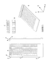
- FIGS 1a, b, c, d and e show different views of a piezoelectric actuator comb 1 with ten separately movable fingers 2.
- Each finger such as that referenced 2 may be displaced at its extremity 3 in essentially the Y direction (see orthogonal coordinate system in figure 1e ). If this actuator is mounted in a horizontal plane in use, the individual fingers 2 will move in the upward and/or downward directions.
- the displacement of the free end of the piezo-finger aims at primarily achieving the tilting of the prism 4. In this sense, the displacement is a side effect with the tilting being the primary object.
- the piezo-fingers act as if they are an arm rotating about an X axis at the centre of the free length of the piezo-fingers.
- the arrangements of figures 2-5 below also cause this mode of tilting.
- the arrangements of figures 6 and 7 use the displacement of the piezo-fingers to generate amplified angle via their flexure arrangements.
- Each finger of comb 1 carries a prism such as that referenced 4 at extremity 3.
- the prism may be attached to this extremity by any appropriate means known to the person skilled in the art.
- the prism 4 as can be best seen in the view of figure 1b , is chopped at its lower extremity 5.
- the prism otherwise is of essentially triangular shape in cross section.
- the line of truncation at extremity 5 extends perpendicularly to the hypotenuse of the triangular shape of the prism.
- each finger is displaceable in simply one dimension in the illustrated embodiment.
- the fingers which in this arrangement displace in one dimension only, may be made to displace in two or three dimensions.
- a two dimensionally displaceable finger may be obtained by employing an actuator of the kind described in WO02/103816 , which is one of the applicant's prior publications.
- Figures 2a, b, c and d show various views of an actuator generally referenced 6 in the form of a piezoelectric comb actuator.
- the comb has a number of fingers such as that referenced 7, each carrying at its extremity 8 a prism 9.
- the piezoelectric comb may operate in a similar fashion to the piezoelectric comb actuator described with regard to figure 1 . It is a particular object of this arrangement to achieve the displacement in one dimension in the Y direction of each individual finger. Since the extremity 8 of each finger is joined to the right angle of a prism 9, any displacement of extremity 8 will cause the displacement of the prism.
- the prism may either be only attached to a piezoelectric comb finger or in addition attached to a separate support structure via a flexure or any other appropriate joining means.
- Figures 3 show various views a, b, c and d of an actuator generally referenced 10.
- Actuator 10 takes the form of a piezoelectric comb actuator with a number of fingers 11 which, at extremity 12, are attached to a reflective element or mirror 13.
- the mirror as shown in the figures, extends perpendicularly from its corresponding finger.
- Mirror 13 may be reflective on any face of the mirror, it is however envisaged that the reflective face is either face 14 or face 15.
- the choice of reflective element and its position relative to its corresponding finger will depend on the application envisaged for this actuator.
- the fingers are designed to displace in both the X and Y directions.
- the two lines along the piezo-actuator finger define the area of the finger which carries out displacement in the X direction whereas the areas above and below these lines are responsible for the displacements in Y directions.
- the fingers may alternatively be one dimensional actuator as in the arrangements of figures 1 and 2 above.
- the actuators may also be entirely separate monolithic structures for displacing each mirror which when supported on a common support structure form a comb.
- Figures 4 show a variety of views of a further actuator 16 incorporating a number of fingers 17 onto each of which is fixed, at its extremity 18, a reflective element 19, which is in this embodiment, a mirror.
- Actuator 16 may operate and be configured in a similar fashion to the actuators of figures 1 , 2 and 3 . Whilst the arrangement shown will achieve one dimensional displacement of extremity 18 of finger 17 in the Y direction, other configurations of fingers or separate actuators may achieve two or three dimensional displacement of the mirror 19.
- figure 5a and 5b show respectively a plan view and a side view of an actuator 20.
- This actuator takes the form of a piezoelectric comb actuator with a number of fingers which are separately displaceable upon actuation.
- Finger 21 is of similar configuration to finger 17 of figure 4a . It supports a reflective element 222 at its extremity 223. Finger 21 is, in this arrangement, a one-dimensionally displaceable beam in the Y direction so that the displacement of finger 21 in the Y direction results in the displacement of mirror 222 in the same direction. Fingers 21 are only provided on alternate fingers of the comb. In this configuration, fingers 22, 23, 24 and 25 are redundant and may in fact be removed if practical to do so.
- Finger 26 and all the other alternate fingers from left to right also do not carry a mirror but are arranged to displace a diagonal linkage arm 27 which extends from an essentially centrally located attachment point (relative to the length of finger 26) to attachment point 29 in close proximity to extremity 23 of finger 21.
- Diagonal linkage arm 27 causes mirror 22 to displace in the X direction when finger 26 is displaced in the Y direction.
- This arrangement achieves two-dimensional displacements of optical elements through a one-dimensional piezo-actuator comb.
- Fingers 230, 231, 232 and 233 also do not contribute to the operation of the optical elements and may therefore be removed if practical.
- attachment point 28 takes the form of a flexible rod 28 of identical height to the reflective element 222.
- Figures 6a and 6b show separate views of an actuator 30 comprising a number of two-dimensional monolithic piezoelectric actuators 31 of the kind described in detail in the applicant's own previous publication referenced above. These are supported by a block 32 on a printed circuit board 33 which may be adapted to drive and sense the position of fingers 31.
- the extremity 34 of finger 31 is attached to a flexure or connecting means 35 which joins extremity 34 to reflective element or mirror 36.
- a second connecting means or flexure 37 attaches mirror 36 to spacer block 38 which extends across the entire array of fingers 31.
- spacer block 39 supports a lower printed circuit board extending across the array of fingers 31 which, together with printed circuit board 41 and vertical plates 42, form a capacitive sensing array which detects changes in capacitance when rods 43, which are attached to the rear of mirrors 36, are displaced inside the housing formed by two vertical plates 42 and portions of the printed circuit boards 40 and 41.
- Spacer block 38 extends beyond spacer block 39 in order to form a step 244 as shown in figure 6b which allows sufficient space for flexing of flexure 37 to take place.
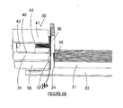
- Figure 7c shows an implementation of an actuator 44 placed in part of an add-drop switch.
- the actuator comprises a 2D piezoelectric finger 45 attached to a support structure 46 through a rear spacer 47.
- a flexure 49 is provided which extends perpendicularly from finger 45. It connects to a linkage arm 50 which holds at its extremity 51 a prism 52.
- a second flexure 53 attaches linkage arm 50 to support structure 46. Since the distance between the flexures 49 and 53 is only approximately 1/6 of the length of linkage arm 50, any displacement of finger 45 will result in amplified displacement at extremity 51. Consequently, prism 52 may be displaced over a relatively large distance with minimal finger deflections.
- prism 52 may be displaced in front of a reflecting element, in this embodiment a mirror 54.
- Figure 7a shows a beam of light reflecting off mirror 54 without prism 52 affecting the light beam.
- actuator 44 displaces prism 52 into the light beam which translates the light beam periscope fashion.
- a key advantage of using the prisms to displace the light is that any tilt, twist or small displacement up/down or in/out has no first order effect on the shifted beam. This reduces the demand on the actuation structure which can be optimised for cost and ruggedness.
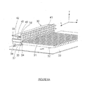
- One application of the actuator of figure 7 is in the wavelength selective arrangement shown in figure 8a and figure 8b .
- a number of input and output collimators such as those referenced 55 and 56 respectively, are used as ports. These are focused towards a point on a collimator mirror 57 which reflects back beams onto an imaging mirror 58 located at the focal length from grating 59.
- Grating 59 is located at 45° to the longitudinal axis. The grating separates light into its constituents once again onto imaging mirror 58 which reflects in turn light towards wavelength plane reflecting element 54.
- a number of prisms 60, 61 and 62 are provided in front of mirror 54 to switch the light from the in/out ports to a pair of add/drop ports.
- the light is shifted up or down by one collimator pitch to couple with a different pair of collimators, for example, add 1/drop 1 (71, 72), add 2/drop 2 (73, 74), add 3/drop 3 (75, 76) or add 4/drop 4 (77, 78) stacked vertically above and below 55 and 56.
- the actuator may take the form of a one-dimensional actuator array of the kind shown in figures 1 to 5 . It may also take the form of an actuator array without any optical element to be inserted into the beams at each wavelength by a variable amount. This would achieve a simple blocker architecture with one input and one output and variable attenuation for each wavelength.
- the reflective element 54 may be replaced by a simple plane mirror 79. Such an arrangement is shown in figures 9a and 9b .
- One possible implementation of these last two arrangements would use a 900 line per millimetre grating angled at 45° to incoming beams with overall dimensions of 8x12mm. It is envisaged to use 1mm diameter collimators operating at a working distance of 100mm. It is also envisaged to use a band spacing of 500GHz, 8 bands across C band, centred at 1,550nm. The distance between the grating 59, mirror 54 and the focusing lens or imaging mirror 58 may be 200mm, 200mm focal length. It is envisaged to have the pitch of the frequency bands on the mirror 54 at 1mm with a total width of 8mm. It is also envisaged to have a beam waist of collimators of approximately 350 ⁇ m diameter with an identical spot size on the imaging mirror. The angle of separation between input and output collimator beams is envisaged to be 15mrad, whilst the separation between collimator centre lines would be 1.5mm.
- piezo-actuator comb whose fingers are 20mm long, with 1mm pitch and with a 0.1mm slot between fingers. Each finger is made of two layers of soft piezoelectric ceramic, each 0.5mm thick. This is driven in parallel mode with a drive voltage swing of 300V, giving a deflection of 0.7mm at the end of the piezoelectric actuator.
- the ends of the piezoelectric actuators are within preferably 1mm of the mirror mounted at an angle of 15° to the horizontal. When in motion, the end of the piezo-actuators move from 0.25mm (zero attenuation state) below beam centre to 0.45mm above (fully blocked state).
- Figure 11 shows a three-dimensional view of a wavelength selective switch using some of the actuators described in the previous arrangements.
- a number of optical fibres 95 couple light to a convergent linear n - way collimator array 96 designed so that beams from all lenses converge on a single point in the plane of the array.
- Each lens is also focused so that each beam goes through a Gaussian beam waist at the same point.
- the array is set up so that one port, for example, the input port, is on a different pitch from the other n-1 ports (output ports).
- 9 output ports are on a 1mm pitch with 1/10 input port offset by 1.5mm so that the input port is out of step with the other 9. This prevents spurious coupling between the output ports when the input port is connected to the third/fifth/seventh etc. output port.
- the beams from the collimators converge on a first folding mirror 97 and then onto a cylindrical mirror 98 which re-images the beam waist from the collimators in one axis (Y) onto the second fold mirror 99 whilst allowing the beams to carry on spreading out in the other axis (X).
- the beam is then reflected off a second folding mirror 99 back onto the cylindrical mirror 98, which again reimages the beams down to a waist in y onto the 3 rd fold mirror 100.
- the beam is reflected off the third folding mirror 100 and then through the cylindrical lens 101, which sends 10 separate near-parallel beams off towards the grating and spherical grating lens 102 which outputs a parallel beam onto the grating, and then provides the focussing needed in the X plane to bring the light to a sharp focus on the array 105.
- the beam is then directed onto a low polarisation-dependent loss, high-efficiency diffraction grating 103 which fans out light at different wavelengths into an angle-to-position lens 104 which directs beams of different wavelengths in parallel directions towards a one-dimensional array of switching mirrors 105.
- This array takes the form of piezoelectric actuator 16 presented in figure 4 above.
- Varying the electric drive to each finger of the actuator changes the angle of the mirror attached to the finger thus the routing of the light at the corresponding wavelength.
- a capacitive position sensor 106 provides electrical feedback from the position of each finger in the actuator. This comb also has a capacitive position sensor (not shown) to ensure linear, stable and hysteresis-free behaviour.
- Light reflecting off array 105 then retraces its path through the system, arriving at the collimator array 96 at a height set by the angle of each mirror element in the array 105.
- the individual wavelengths on the input are directed to outputs 1 through 9.
- One dimensional piezoelectric comb 107 is located in close proximity to actuator 105 and is configured so that when driven at an appropriate level each finger is raised up blocking light at a corresponding wavelength altogether. Alternatively, if the finger is not in the blocking position, it will allow light to hit the appropriate optical element 105. This allows light at the relevant wavelength from the input ports to be blocked whilst a switch mirror changes position, thus preventing unwanted dynamic cross-talk as the mirror swings past the intermediate ports between the old and new destination ports.
- An array of the kind presented in figure 4 may incorporate beneath its fingers an insulating substrate 108 plated with an array of metal tracks 109 parallel to the comb fingers when the actuator fingers are not deflected.
- the electrical connections of the tracks apply AC stimulus wave forms having the same frequency but relative phases of 0°, 90°, 180° and 270° to alternate tracks.
- the remaining tracks are connected in pairs to a low-noise op-amp.
- the op-amp is configured so that its output is proportional to the sum of the capacitive couplings between the tracks connected to its input and the adjacent stimulus track.
- a low impedance (at the stimulus frequency) connection is made from the fingers of the piezo-comb to ground.
- an array of non-convergent collimators 110 may be used to direct light onto an additional lens 111 placed in front of the array to cause the beams to converge to a point.
- an additional lens 111 placed in front of the array to cause the beams to converge to a point.
- the positions of the Gaussian beam waists from the collimator array may be adjusted to be in front of or behind the point where all beams intersect.
- flexures are used to attach the mirrors to the comb.
- a piezoelectric ceramic finger 112 is secured at one extremity to a support structure 113 through a spacer 114.
- Finger 112 incorporates a flexure 115 extending perpendicularly from the free extremity of finger 112 and attaches a glass block 116.
- a second flexure 117 is used at the forward most face of block 116 to secure block 116 to the support structure 113.
- the assembly may be made as described above, with a single piezo-ceramic being bonded to two single flexures as one single block before the whole assembly is sawn into a number of fingers.
- the rear flexure 115 may be pre-formed with a number of discrete tabs for attaching to each tooth of a pre-made piezoelectric comb.
- the mirror and flexures can then be bonded and sawn before attachment to the piezoelectric comb.
- the flexures are set up so that movement of the piezoelectric comb's fingers in one axis (for example up/down) is transmitted to the mirror whilst stray movements in other axes (for example in/out of the page are not coupled).
- the glass block may be mirrored to reflect light perpendicular to the piezo fingers as shown in beam path 119 and parallel to them as shown by beam path 118.
- the block side corresponding to path 118 may be used in 1-dimensional block motion mode whereas the block side corresponding to path 119 may be used in 2-dimensional block motion mode as well as 1-dimensional block motion mode if practical to do so.
- the piezo/mirror assembly can be sawn on a non-uniform pitch.
- the piezoelectric comb may be sawn at a fixed pitch and a mirror assembly may be sawn at a non-uniform pitch. These are then attached to each other.
- the arrangement also envisages the use of sensors at locations 120 and 121 in a forward spaced location from the front face of block 116 and in a spaced position beneath block 116 for sensor 121.
- sensors may be installed at both of these positions and use a differential scheme discussed above.
- a position sensing arrangement is also envisaged between board portions 139 and piezo-actuator portions 138.
- figure 15b it may be possible to extend one of the flexures 122 beyond the glass block 123 and to use a differential sensor design 124 to sense the position of this flexure and thus infer the position of the glass block 123.
- the arrangement of figure 15b is particularly suited when employed with a 2 dimensional piezo-finger.
- Figure 15c shows a further arrangement where a flexure 122' extends forwardly from the glass block 123' into a differential position sensor 124'.
- This design is particularly suited when employed with a 1 dimensional piezo-finger. These may be used instead of the sensing arrangement located beneath the fingers as shown in figure 14a and referenced 138 and 139.
- each piezoelectric finger is capable of moving in two dimensions: both up and down relative to the plane of the comb, and left and right within the comb.
- Figure 15a shows a position sensing scheme suitable for two axes movement monitoring.
- FIGs 16a and b show a wavelength selective switch in accordance with an embodiment of the invention.
- the switch comprises an input collimator 125 which may send a beam of light through a cylindrical lens 126 onto a spherical mirror 127. The light is then reflected onto a grating 128 and back onto spherical mirror 127. The light then passes through cylindrical lens 129 prior to tipping mirror array 130 which can be based on either of the arrangements shown in Figures 5 and 6 , as described in this application. The light then retraces its path through the system to one of nine output collimators 125a...125i depending on the angle of the individual array mirror element 130.
- the distances can be: a) approximately 1.5 - 10.5mm; b) 115mm; c) 65mm; d) approximately 1 - 2mm; e) 1.3mm; f) 66mm; g) approximately 1.5 - 10.5mm and h) approximately 1000mm. These distances are used as an example of appropriate distances without intending to be limiting.
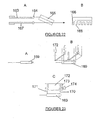
- FIGs 17a and b show a multiple piezoelectric laser scanner 131 comprising two oppositely placed actuators 132 and 133.
- Each actuator is in the form of a piezoelectric comb where each finger 134 terminates in a reflective element or mirror 135, the piezoelectric combs of these actuators are preferably constructed by initially attaching the mirrors 135 to a block of piezoelectric material prior to diamond sawing the slots to make the separate fingers of the comb.
- Each finger of the comb is driven by appropriate electric means to achieve two dimensional displacements of the mirrors.
- Figures 18a and b show the piezoelectric laser scanner with the fingers in a deflected mode as well as the electronic driving circuitry.
- Figure 17b also shows the layers of conductors, such as that referenced 136, and the base plate 137 onto which the actuator arrays are mounted.
- Figure 19 also shows the conductor layers within the actuator array interleaved with piezoelectric ceramic material necessary to achieve up (U), down (D), left (L) and right (R) displacements of the individual fingers.
- a scanner can be made capable of 0.1 radian total scan angle in both axes having a bandwidth of approximately 15kHz.
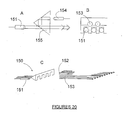
- Figure 20C shows a bank 150 of optical elements as collimators 151 placed at a pitch of 2 mm in front of the slots of a slotted prism (a slotted right prism in this arrangement).
- a bank 152 of optical elements as collimators 153 are also provided placed at a pitch of 2mm to direct light between the slots of the prism so that the light bounces of face 154 and 155.
- the resultant output beams' array of this arrangement results in a beam array at a pitch of only 1mm. In other words, the output array has a pitch of half the pitch of the input collimators.
- Figures 21 show an alternate interleaved arrangement where actuator 156 comprises a reflector 157 for directing light onto the finger 158 of a slotted mirror 160 whilst actuator 159 comprises a reflector 161 for directing light between the fingers of the slotted mirror or through a slot of the mirror in order to be reflected by rear mirror 162.
- the actuators are spaced at a pitch of 2mm and achieve through this arrangement output beams at a pitch of 1mm.
- Figures 22 show a further interleaved arrangement where actuator 163 uses a reflector 164 to direct light onto a slotted glass block 165 which directs light out through one of its fingers 166.
- This arrangement uses a second actuator 167 which directs light between the fingers through the slots 168 so that whilst the pitch of the actuators is 2mm the pitch of the output beams is only 1mm.
- interleaved arrangement above may be used with a variety of inputs such as collimators or reflectors or any other appropriate input as selected by the person skilled in the art from known alternatives.
- Figures 23 show a collimator 169 which is to be held in position by flexures such those referenced 170 and 171 which attach at the front and rear of the collimator respectively and extend upwards to be held by a clamping block 172.
- the block incorporates a number of clamps 173 to grip a flexure by adjusting the bolt 174.
- This arrangement may be employed to permit fine adjustment in manufacture of the x and y pointing angle and x and y position (i.e. 4 axes in total).
Landscapes
- Physics & Mathematics (AREA)
- General Physics & Mathematics (AREA)
- Optics & Photonics (AREA)
- Nonlinear Science (AREA)
- Engineering & Computer Science (AREA)
- Computer Networks & Wireless Communication (AREA)
- Mechanical Light Control Or Optical Switches (AREA)
Description
- The invention relates to optical wavelength selective switches.
- The applicant's own previously published patent documents such as
WO01/50176 WO02/46825 WO02/103816 WO03/104872 WO02/103816 WO03/104872 - Other prior art documents show devices for spreading light from a fibre into different frequency components via a diffraction grating which rely on the modulation of the intensity of each component using either liquid crystal display (LCD) arrays or linear arrays of tilting mirror elements which directly re-image the spectrum from the diffraction grating into another fibre.
US6,661,948 (Capella Photonics Incorporated) uses a diffraction grating and an array of micro-mirrors which are individually and continuously controllable. Such systems rely on so-called micro-electro-mechanical (MEMs) systems. Other similar publications exist such as:U6,695,457 ,US6,687,431 ,US6,625,346 ,US6,549,699 ,US6,507,685 ,US6,504,976 andUS2002/0131698 . Similarly,US6,535,311 (Corning Incorporated) also relies on the use of MEMs systems which in this publication takes the form of a shutter array. Furthermore,US6,711,316 (JDS Uniphase Incorporated) also relies on the use of deflector arrays, either liquid crystal, phase arrays or reflective MEMS arrays. This is also the case for patent documentUS6,707,959 (JDS Uniphase Incorporated) which relies on the use of MEMS.US6,204,946 (Lucent Technologies Incorporated) also requires the use of MEMs for receiving multiple-wavelength signals and selectively switching between a transmission mode and a reflection mode. - Another piece of prior art is disclosed in
US6,661,953 (Avanex Corporation). This document shows an apparatus with at least one input fibre; a lens optically coupled to at least one input fibre; a diffraction grating selectively coupled to the lens at a side opposite to at least one input fibre; at least one output fibre optically coupled to the lens at the side opposite to the diffraction grating and a plurality of movable rods residing at the side of the lens opposite to the diffraction grating, wherein the plurality of movable rods is capable of intercepting a variable portion of a light traversing through the lens. Whilst this document mentions that their movable rod array may be fabricated as a micro-electro-mechanical system, it may also be fabricated as a set of bendable piezoelectric rods. The system shown however envisages only inputs/outputs from optical fibres; shows the use of a simple piezoelectric comb without any reflective elements and is concerned primarily with optical detection or attenuation of wavelength channels. - The following prior art documents are acknowledged:
US6501877 which shows a wavelength selective optical switch comprising a dispersive means and an actuator in the form of a comb array of one dimensionally displaceable fingers, each having an optical element which directs an individual wavelength to one of a plurality of output ports,US2003/0173865 ; andUS2003/108284 . - In a first broad independent aspect, the invention is defined in
claim 1. - This arrangement is particularly advantageous because it allows optical switches to be configured of bulk optical components such as lenses, collimators, prisms and bulk mirrors to achieve comparable levels of accuracy to switches necessarily incorporating MEMs elements. This also reduces the required level of tolerances and simplifies the manufacturing and servicing requirements, which has considerable cost benefits.
- In a further subsidiary aspect, the fingers are part of a comb array.
- In a further subsidiary aspect, the or each optical element is a reflective element.
- In a further subsidiary aspect, the or each optical element is a prism. One of the advantages of using a prism for such an arrangement is that it allows the light to be displaced whilst any tilt, twist or small displacement up/down or in/out has no first order effect on the shifted beam.
- In a further subsidiary aspect, the or each reflective element is attached to the finger by a flexure means. This would allow a flexible attachment to be achieved which may be used to achieve repeatable amplification of any deflection at the extremity of the finger.
- In another subsidiary aspect, the reflective element is a mirror. The use of a mirror rather than a micro-machined array of mirrors also has the advantages of minimal demand on the actuation structure which allows the system to operate with a high level of accuracy even without these components.
- In a further subsidiary aspect, the or each mirror extends substantially perpendicularly to the longitudinal axis of the fingers.
- In a further subsidiary aspect, the or each mirror is mounted along the axis of the corresponding finger.
- In a second broad independent aspect, the invention is defined in
claim 2. One of the advantages of this configuration is that it allows an array of one dimensional actuators to achieve the two dimensional movements of optical elements. - In a further subsidiary aspect of the first broad independent aspect, the one or more optical elements are equipped with a rod extending from the element into a housing equipped with means for sensing the position of the rod within said housing. This allows position feedback to be obtained for adjustments to take place in order to achieve high/adjustable levels of accuracy.
- In a further subsidiary aspect, electrical sensing means are provided to sense the position of the fingers. This allows more accurate positioning of the optical elements.
- In a subsidiary aspect, the reflective element is a prism.
- In a subsidiary aspect, the reflective element is a mirror.
-
- Figures 1a, b, c, d and e show an actuator comb with a truncated prism on each finger of the comb in plan, side elevation, front elevation, rear elevation and perspective view respectively.
- Figures 2a, b, c and d show an actuator comb where each finger carries a prism in plan, side elevation, front elevation and perspective view respectively.
- Figures 3a, b, c and d show an actuator comb with each finger carrying a perpendicularly placed mirror in plan, front elevation, side elevation and perspective view respectively.
- Figures 4a, b, c and d show an actuator in plan, side elevation, front elevation and perspective view respectively.
-
Figure 5a shows a plan view of an actuator comb with linkage arms where the fingers are individually displaceable in one dimension to achieve the 2-dimensional displacement of an optical element. -
Figure 5b shows a side view of the actuator offigure 5a . -
Figure 6a shows a perspective view of an actuator with an array of mirrors. -
Figure 6b shows a perspective side view of the rear portion of the actuator offigure 6b . - Figures 7a, b and c show schematically side views of a switch element using a prism.
-
Figure 8a shows a plan view of a wavelength selective switch using actuated prisms. -
Figure 8b shows a side view of the switch offigure 8a . -
Figure 9a shows a plan view of an optical wavelength selective blocker switch. -
Figure 9b shows a side view of the switch offigure 9a . -
Figures 10a and 10b show respectively a top and side view of an optical wavelength selective switch portion using prisms and a piezoelectric comb as a blocker. -
Figure 11 shows a wavelength selective switch. -
Figure 12 shows a position sensing arrangement around the fingers of an actuator comb; the fingers in the figure being shown in cross section. -
Figure 13 shows the use of n-way-collimator arrays in both convergent mode and parallel mode. -
Figure 14a shows a schematic cross-sectional view of a finger for displacing a mirror block. -
Figure 14b shows a possible circuit for sensing the position of the various elements of the arrangement offigure 14a . -
Figure 15a shows the sensing arrangement for a 2-dimensionally displaceable finger array. -
Figure 15b shows a side view of a further sensing arrangement for sensing the position of a block. -
Figures 16a and 16b respectively show a plan view and a side view of a wavelength selective switch using a tilting mirror in accordance with an embodiment of the invention. -
Figures 17a and 17b show an arrangement of two piezoelectric combs forming a scanner in a plan view and a side cross-sectional view respectively. -
Figures 18a and 18b show the embodiment offigure 17 where the fingers of the piezoelectric comb actuator are flexed. -
Figure 19 shows a schematic representation of the electrode plates and piezoelectric layers in cross-sectional view of the five finger comb actuator offigures 17 and18 . - Figures 20a, b and c show an array of optical inputs associated with a slotted prism in schematic side view, side view and perspective view respectively.
-
Figures 21 a and b show an array of optical inputs associated with a slotted mirror in schematic side/cross-sectional view and the slotted optical elements in perspective view respectively. - Figures 22a and b show an array of optical inputs associated with a slotted glass block in side/cross-sectional view and front view respectively.
- Figures 23a, b and c show an array of a collimator and mounting block in perspective view (b) and side/cross-sectional view (c).
- Figures 1a, b, c, d and e show different views of a
piezoelectric actuator comb 1 with ten separatelymovable fingers 2. Each finger such as that referenced 2 may be displaced at itsextremity 3 in essentially the Y direction (see orthogonal coordinate system infigure 1e ). If this actuator is mounted in a horizontal plane in use, theindividual fingers 2 will move in the upward and/or downward directions. The displacement of the free end of the piezo-finger aims at primarily achieving the tilting of the prism 4. In this sense, the displacement is a side effect with the tilting being the primary object. In order to obtain adequate ratio of rotation to displacement, the piezo-fingers act as if they are an arm rotating about an X axis at the centre of the free length of the piezo-fingers. The arrangements offigures 2-5 below also cause this mode of tilting. By contrast, the arrangements offigures 6 and7 , use the displacement of the piezo-fingers to generate amplified angle via their flexure arrangements. - Each finger of
comb 1 carries a prism such as that referenced 4 atextremity 3. The prism may be attached to this extremity by any appropriate means known to the person skilled in the art. In this arrangement, the prism 4, as can be best seen in the view offigure 1b , is chopped at itslower extremity 5. The prism otherwise is of essentially triangular shape in cross section. The line of truncation atextremity 5 extends perpendicularly to the hypotenuse of the triangular shape of the prism. - As mentioned above, each finger is displaceable in simply one dimension in the illustrated embodiment. However, it is also envisaged that the fingers, which in this arrangement displace in one dimension only, may be made to displace in two or three dimensions. A two dimensionally displaceable finger may be obtained by employing an actuator of the kind described in
WO02/103816 - Figures 2a, b, c and d show various views of an actuator generally referenced 6 in the form of a piezoelectric comb actuator. The comb has a number of fingers such as that referenced 7, each carrying at its extremity 8 a
prism 9. The piezoelectric comb may operate in a similar fashion to the piezoelectric comb actuator described with regard tofigure 1 . It is a particular object of this arrangement to achieve the displacement in one dimension in the Y direction of each individual finger. Since theextremity 8 of each finger is joined to the right angle of aprism 9, any displacement ofextremity 8 will cause the displacement of the prism. In both the arrangements offigures 1 and2 , the prism may either be only attached to a piezoelectric comb finger or in addition attached to a separate support structure via a flexure or any other appropriate joining means. -
Figures 3 show various views a, b, c and d of an actuator generally referenced 10.Actuator 10 takes the form of a piezoelectric comb actuator with a number offingers 11 which, atextremity 12, are attached to a reflective element ormirror 13. The mirror, as shown in the figures, extends perpendicularly from its corresponding finger.Mirror 13 may be reflective on any face of the mirror, it is however envisaged that the reflective face is eitherface 14 orface 15. The choice of reflective element and its position relative to its corresponding finger will depend on the application envisaged for this actuator. - In this arrangement, the fingers are designed to displace in both the X and Y directions. The two lines along the piezo-actuator finger define the area of the finger which carries out displacement in the X direction whereas the areas above and below these lines are responsible for the displacements in Y directions. The fingers may alternatively be one dimensional actuator as in the arrangements of
figures 1 and2 above. The actuators may also be entirely separate monolithic structures for displacing each mirror which when supported on a common support structure form a comb. -
Figures 4 show a variety of views of afurther actuator 16 incorporating a number offingers 17 onto each of which is fixed, at itsextremity 18, areflective element 19, which is in this embodiment, a mirror.Actuator 16 may operate and be configured in a similar fashion to the actuators offigures 1 ,2 and3 . Whilst the arrangement shown will achieve one dimensional displacement ofextremity 18 offinger 17 in the Y direction, other configurations of fingers or separate actuators may achieve two or three dimensional displacement of themirror 19. - The following two figures,
figure 5a and 5b , show respectively a plan view and a side view of anactuator 20. This actuator takes the form of a piezoelectric comb actuator with a number of fingers which are separately displaceable upon actuation.Finger 21 is of similar configuration tofinger 17 offigure 4a . It supports areflective element 222 at itsextremity 223.Finger 21 is, in this arrangement, a one-dimensionally displaceable beam in the Y direction so that the displacement offinger 21 in the Y direction results in the displacement ofmirror 222 in the same direction.Fingers 21 are only provided on alternate fingers of the comb. In this configuration,fingers Finger 26 and all the other alternate fingers from left to right also do not carry a mirror but are arranged to displace adiagonal linkage arm 27 which extends from an essentially centrally located attachment point (relative to the length of finger 26) toattachment point 29 in close proximity toextremity 23 offinger 21.Diagonal linkage arm 27 causes mirror 22 to displace in the X direction whenfinger 26 is displaced in the Y direction. This arrangement achieves two-dimensional displacements of optical elements through a one-dimensional piezo-actuator comb. Fingers 230, 231, 232 and 233 also do not contribute to the operation of the optical elements and may therefore be removed if practical. -
Figure 5b has retained the same numerical references as used with reference tofigure 5a for ease of understanding. In this figure,attachment point 28 takes the form of aflexible rod 28 of identical height to thereflective element 222. -
Figures 6a and6b show separate views of anactuator 30 comprising a number of two-dimensional monolithicpiezoelectric actuators 31 of the kind described in detail in the applicant's own previous publication referenced above. These are supported by ablock 32 on a printedcircuit board 33 which may be adapted to drive and sense the position offingers 31. Theextremity 34 offinger 31 is attached to a flexure or connectingmeans 35 which joinsextremity 34 to reflective element ormirror 36. A second connecting means orflexure 37 attachesmirror 36 tospacer block 38 which extends across the entire array offingers 31. Stacked ontospacer block 38,spacer block 39 supports a lower printed circuit board extending across the array offingers 31 which, together with printedcircuit board 41 andvertical plates 42, form a capacitive sensing array which detects changes in capacitance whenrods 43, which are attached to the rear ofmirrors 36, are displaced inside the housing formed by twovertical plates 42 and portions of the printedcircuit boards Spacer block 38 extends beyondspacer block 39 in order to form a step 244 as shown infigure 6b which allows sufficient space for flexing offlexure 37 to take place. - In this configuration, when
finger 31 displaces in the X direction, it will causemirror 36 to tilt in the X/Y plane and whenfinger 31 displaces in the Y direction, it will cause the mirror to tilt in the Y/ Z plane. -
Figure 7c shows an implementation of anactuator 44 placed in part of an add-drop switch. The actuator comprises a2D piezoelectric finger 45 attached to asupport structure 46 through arear spacer 47. Atextremity 48 offinger 45, aflexure 49 is provided which extends perpendicularly fromfinger 45. It connects to alinkage arm 50 which holds at its extremity 51 aprism 52. Asecond flexure 53 attacheslinkage arm 50 to supportstructure 46. Since the distance between theflexures linkage arm 50, any displacement offinger 45 will result in amplified displacement atextremity 51. Consequently,prism 52 may be displaced over a relatively large distance with minimal finger deflections. In this configuration,prism 52 may be displaced in front of a reflecting element, in this embodiment amirror 54.Figure 7a shows a beam of light reflecting offmirror 54 withoutprism 52 affecting the light beam. Infigure 7b actuator 44 displacesprism 52 into the light beam which translates the light beam periscope fashion. A key advantage of using the prisms to displace the light is that any tilt, twist or small displacement up/down or in/out has no first order effect on the shifted beam. This reduces the demand on the actuation structure which can be optimised for cost and ruggedness. One application of the actuator offigure 7 is in the wavelength selective arrangement shown infigure 8a andfigure 8b . - A number of input and output collimators, such as those referenced 55 and 56 respectively, are used as ports. These are focused towards a point on a
collimator mirror 57 which reflects back beams onto animaging mirror 58 located at the focal length from grating 59.Grating 59 is located at 45° to the longitudinal axis. The grating separates light into its constituents once again ontoimaging mirror 58 which reflects in turn light towards wavelengthplane reflecting element 54. A number ofprisms mirror 54 to switch the light from the in/out ports to a pair of add/drop ports. The light is shifted up or down by one collimator pitch to couple with a different pair of collimators, for example, add 1/drop 1 (71, 72), add 2/drop 2 (73, 74), add 3/drop 3 (75, 76) or add 4/drop 4 (77, 78) stacked vertically above and below 55 and 56. - Instead of using two-dimensional displacement actuators for each prism, the actuator may take the form of a one-dimensional actuator array of the kind shown in
figures 1 to 5 . It may also take the form of an actuator array without any optical element to be inserted into the beams at each wavelength by a variable amount. This would achieve a simple blocker architecture with one input and one output and variable attenuation for each wavelength. In this version, thereflective element 54 may be replaced by asimple plane mirror 79. Such an arrangement is shown infigures 9a and9b . In this configuration, there are two input/output ports collimator mirror 82, animaging mirror 83, a grating 84 and a one-dimensional actuator array 85 which can displace into or out of the path of individual wavelength light beams. - One possible implementation of these last two arrangements would use a 900 line per millimetre grating angled at 45° to incoming beams with overall dimensions of 8x12mm. It is envisaged to use 1mm diameter collimators operating at a working distance of 100mm. It is also envisaged to use a band spacing of 500GHz, 8 bands across C band, centred at 1,550nm. The distance between the grating 59,
mirror 54 and the focusing lens orimaging mirror 58 may be 200mm, 200mm focal length. It is envisaged to have the pitch of the frequency bands on themirror 54 at 1mm with a total width of 8mm. It is also envisaged to have a beam waist of collimators of approximately 350µm diameter with an identical spot size on the imaging mirror. The angle of separation between input and output collimator beams is envisaged to be 15mrad, whilst the separation between collimator centre lines would be 1.5mm. - It is also envisaged to use a piezo-actuator comb whose fingers are 20mm long, with 1mm pitch and with a 0.1mm slot between fingers. Each finger is made of two layers of soft piezoelectric ceramic, each 0.5mm thick. This is driven in parallel mode with a drive voltage swing of 300V, giving a deflection of 0.7mm at the end of the piezoelectric actuator. The ends of the piezoelectric actuators are within preferably 1mm of the mirror mounted at an angle of 15° to the horizontal. When in motion, the end of the piezo-actuators move from 0.25mm (zero attenuation state) below beam centre to 0.45mm above (fully blocked state). This description also envisages the addition of a quarter wave plate to the front face of the mirror with its axis aligned at 45° to the horizontal. This allows the axis of polarisation to rotate by 90° between the two passages over the attenuating fingers because the light passes through the wave plate twice. This allows the first order polarisation-dependent loss created by fingers in the semi-blocked state to be cancelled whilst also cancelling the first order polarisation-dependent loss (PDL) introduced by the grating. The functions shown respectively in
figures 7 to 8b and 9a and 9b (flexible add drop and variable attenuation) can be combined in the same unit as shown infigures 10a and b by making all the prism displacements in the same direction and placing the attenuating fingers in front. In this figure there is provided a wavelength planereflective element 86, ablocker array 89, aprism actuator 90 andprisms -
Figure 11 shows a three-dimensional view of a wavelength selective switch using some of the actuators described in the previous arrangements. A number ofoptical fibres 95 couple light to a convergent linear n -way collimator array 96 designed so that beams from all lenses converge on a single point in the plane of the array. Each lens is also focused so that each beam goes through a Gaussian beam waist at the same point. The array is set up so that one port, for example, the input port, is on a different pitch from the other n-1 ports (output ports). For example, 9 output ports are on a 1mm pitch with 1/10 input port offset by 1.5mm so that the input port is out of step with the other 9. This prevents spurious coupling between the output ports when the input port is connected to the third/fifth/seventh etc. output port. - The beams from the collimators converge on a
first folding mirror 97 and then onto acylindrical mirror 98 which re-images the beam waist from the collimators in one axis (Y) onto the second fold mirror 99 whilst allowing the beams to carry on spreading out in the other axis (X). The beam is then reflected off a second folding mirror 99 back onto thecylindrical mirror 98, which again reimages the beams down to a waist in y onto the 3rdfold mirror 100. Subsequently, the beam is reflected off thethird folding mirror 100 and then through thecylindrical lens 101, which sends 10 separate near-parallel beams off towards the grating and sphericalgrating lens 102 which outputs a parallel beam onto the grating, and then provides the focussing needed in the X plane to bring the light to a sharp focus on thearray 105. The beam is then directed onto a low polarisation-dependent loss, high-efficiency diffraction grating 103 which fans out light at different wavelengths into an angle-to-position lens 104 which directs beams of different wavelengths in parallel directions towards a one-dimensional array of switching mirrors 105. This array takes the form ofpiezoelectric actuator 16 presented infigure 4 above. Varying the electric drive to each finger of the actuator changes the angle of the mirror attached to the finger thus the routing of the light at the corresponding wavelength. Acapacitive position sensor 106 provides electrical feedback from the position of each finger in the actuator. This comb also has a capacitive position sensor (not shown) to ensure linear, stable and hysteresis-free behaviour. - Light reflecting off
array 105 then retraces its path through the system, arriving at thecollimator array 96 at a height set by the angle of each mirror element in thearray 105. By this means, the individual wavelengths on the input are directed tooutputs 1 through 9. - One dimensional
piezoelectric comb 107, without any optical elements, is located in close proximity toactuator 105 and is configured so that when driven at an appropriate level each finger is raised up blocking light at a corresponding wavelength altogether. Alternatively, if the finger is not in the blocking position, it will allow light to hit the appropriateoptical element 105. This allows light at the relevant wavelength from the input ports to be blocked whilst a switch mirror changes position, thus preventing unwanted dynamic cross-talk as the mirror swings past the intermediate ports between the old and new destination ports. - An array of the kind presented in
figure 4 may incorporate beneath its fingers an insulatingsubstrate 108 plated with an array ofmetal tracks 109 parallel to the comb fingers when the actuator fingers are not deflected. The electrical connections of the tracks apply AC stimulus wave forms having the same frequency but relative phases of 0°, 90°, 180° and 270° to alternate tracks. The remaining tracks are connected in pairs to a low-noise op-amp. The op-amp is configured so that its output is proportional to the sum of the capacitive couplings between the tracks connected to its input and the adjacent stimulus track. A low impedance (at the stimulus frequency) connection is made from the fingers of the piezo-comb to ground. As the fingers move up and down, the amount of coupling between the stimulus tracks and the op-amp input varies. This causes the op-amp output to vary in the fashion indicated in the graph offigure 12 . It can be seen that varying the positions of each of the two fingers associated with any one op-amp produces orthogonal variations in that op-amp's output, thus allowing the position of the two fingers to be independently determined. - As shown in
figure 13 , instead of using a convergent linear n-way collimator array 96, an array ofnon-convergent collimators 110 may be used to direct light onto anadditional lens 111 placed in front of the array to cause the beams to converge to a point. By appropriate choice of the lens focal length and the separation of the lens and the collimator array, it is possible to ensure that all beams pass through a Gaussian beam waist at the same point as they all intersect. A comparison of aconvergent collimator array 96 and aparallel collimator array 110 is shown infigure 13 . - To compensate for under/over focusing of light in the system, the positions of the Gaussian beam waists from the collimator array may be adjusted to be in front of or behind the point where all beams intersect.
- In an arrangement that does not form part of the invention, instead of being bonded directly to the comb, flexures are used to attach the mirrors to the comb. An example of this can be seen in
figure 14a . A piezoelectricceramic finger 112 is secured at one extremity to asupport structure 113 through aspacer 114.Finger 112 incorporates aflexure 115 extending perpendicularly from the free extremity offinger 112 and attaches aglass block 116. Asecond flexure 117 is used at the forward most face ofblock 116 to secureblock 116 to thesupport structure 113. The assembly may be made as described above, with a single piezo-ceramic being bonded to two single flexures as one single block before the whole assembly is sawn into a number of fingers. Alternatively, therear flexure 115 may be pre-formed with a number of discrete tabs for attaching to each tooth of a pre-made piezoelectric comb. The mirror and flexures can then be bonded and sawn before attachment to the piezoelectric comb. In all cases, the flexures are set up so that movement of the piezoelectric comb's fingers in one axis (for example up/down) is transmitted to the mirror whilst stray movements in other axes (for example in/out of the page are not coupled). The glass block may be mirrored to reflect light perpendicular to the piezo fingers as shown inbeam path 119 and parallel to them as shown bybeam path 118. The block side corresponding topath 118 may be used in 1-dimensional block motion mode whereas the block side corresponding topath 119 may be used in 2-dimensional block motion mode as well as 1-dimensional block motion mode if practical to do so. - As mentioned above with reference to
figure 11 , the light coming from the diffraction grating is spread out by wavelength. However, the amount by which different wavelengths are separated is not perfectly uniform across a band of wavelengths. To compensate for this, the piezo/mirror assembly can be sawn on a non-uniform pitch. Alternatively, the piezoelectric comb may be sawn at a fixed pitch and a mirror assembly may be sawn at a non-uniform pitch. These are then attached to each other. - It is also possible to place an array of sensing tracks above the piezo comb fingers as well as below them. A differential sensor, as shown in
figure 14b , can be implemented. The advantage of using such an arrangement is that it yields improved signal-to-noise performance over the original sensing scheme discussed above. - Returning to
figure 14a , the arrangement also envisages the use of sensors atlocations block 116 and in a spaced position beneathblock 116 forsensor 121. Alternatively, sensors may be installed at both of these positions and use a differential scheme discussed above. A position sensing arrangement is also envisaged betweenboard portions 139 and piezo-actuator portions 138. - Further, alternatively, as shown in
figure 15b , it may be possible to extend one of theflexures 122 beyond theglass block 123 and to use adifferential sensor design 124 to sense the position of this flexure and thus infer the position of theglass block 123. The arrangement offigure 15b is particularly suited when employed with a 2 dimensional piezo-finger. -
Figure 15c shows a further arrangement where a flexure 122' extends forwardly from the glass block 123' into a differential position sensor 124'. This design is particularly suited when employed with a 1 dimensional piezo-finger. These may be used instead of the sensing arrangement located beneath the fingers as shown infigure 14a and referenced 138 and 139. - According to the invention, each piezoelectric finger is capable of moving in two dimensions: both up and down relative to the plane of the comb, and left and right within the comb. In this embodiment, it is possible to change which output port the input port is coupled to without steering the light from the input port across intermediate output ports in the process. The need for the blocker comb is then avoided.
Figure 15a shows a position sensing scheme suitable for two axes movement monitoring. - Figures 16a and b show a wavelength selective switch in accordance with an embodiment of the invention. The switch comprises an
input collimator 125 which may send a beam of light through acylindrical lens 126 onto aspherical mirror 127. The light is then reflected onto a grating 128 and back ontospherical mirror 127. The light then passes throughcylindrical lens 129 prior totipping mirror array 130 which can be based on either of the arrangements shown inFigures 5 and6 , as described in this application. The light then retraces its path through the system to one of nineoutput collimators 125a...125i depending on the angle of the individualarray mirror element 130. In this embodiment, the distances can be: a) approximately 1.5 - 10.5mm; b) 115mm; c) 65mm; d) approximately 1 - 2mm; e) 1.3mm; f) 66mm; g) approximately 1.5 - 10.5mm and h) approximately 1000mm. These distances are used as an example of appropriate distances without intending to be limiting. - Figures 17a and b show a multiple
piezoelectric laser scanner 131 comprising two oppositely placedactuators finger 134 terminates in a reflective element ormirror 135, the piezoelectric combs of these actuators are preferably constructed by initially attaching themirrors 135 to a block of piezoelectric material prior to diamond sawing the slots to make the separate fingers of the comb. Each finger of the comb is driven by appropriate electric means to achieve two dimensional displacements of the mirrors. Figures 18a and b show the piezoelectric laser scanner with the fingers in a deflected mode as well as the electronic driving circuitry. -
Figure 17b also shows the layers of conductors, such as that referenced 136, and thebase plate 137 onto which the actuator arrays are mounted.Figure 19 also shows the conductor layers within the actuator array interleaved with piezoelectric ceramic material necessary to achieve up (U), down (D), left (L) and right (R) displacements of the individual fingers. - Using a pair of five finger actuator combs with a pitch of 1mm, the fingers being 0.9mm thick and 3mm long, a scanner can be made capable of 0.1 radian total scan angle in both axes having a bandwidth of approximately 15kHz.
-
Figure 20C shows abank 150 of optical elements ascollimators 151 placed at a pitch of 2 mm in front of the slots of a slotted prism (a slotted right prism in this arrangement). Abank 152 of optical elements ascollimators 153 are also provided placed at a pitch of 2mm to direct light between the slots of the prism so that the light bounces offace -
Figures 21 show an alternate interleaved arrangement whereactuator 156 comprises areflector 157 for directing light onto thefinger 158 of a slottedmirror 160 whilstactuator 159 comprises areflector 161 for directing light between the fingers of the slotted mirror or through a slot of the mirror in order to be reflected byrear mirror 162. The actuators are spaced at a pitch of 2mm and achieve through this arrangement output beams at a pitch of 1mm. -
Figures 22 show a further interleaved arrangement whereactuator 163 uses areflector 164 to direct light onto a slottedglass block 165 which directs light out through one of itsfingers 166. This arrangement uses asecond actuator 167 which directs light between the fingers through theslots 168 so that whilst the pitch of the actuators is 2mm the pitch of the output beams is only 1mm. - The interleaved arrangement above may be used with a variety of inputs such as collimators or reflectors or any other appropriate input as selected by the person skilled in the art from known alternatives.
-
Figures 23 show acollimator 169 which is to be held in position by flexures such those referenced 170 and 171 which attach at the front and rear of the collimator respectively and extend upwards to be held by aclamping block 172. The block incorporates a number ofclamps 173 to grip a flexure by adjusting thebolt 174. This arrangement may be employed to permit fine adjustment in manufacture of the x and y pointing angle and x and y position (i.e. 4 axes in total).
Claims (11)
- A wavelength selective optical switch comprising one or more input ports (125) for directing an optical beam into the switch;
a plurality of output ports (125a-125i);
dispersive means (128) configured to receive said optical beam and to spatially separate the optical beam into individual wavelength components,
an actuator (130) towards which said individual wavelength components are routed, said actuator being in the form of an array of elongate movable fingers (31)
, one or more of said elongate movable fingers displacing an optical element (36), each of which directs one of said individual wavelength components to one or more selected output ports of said plurality of output ports,
characterised in that said fingers (31) are monolithic piezoelectric actuators displaceable in two dimensions, said one or more of said fingers having a first connecting means (35) to said optical element (36), and in that the wavelength selective switch further comprises a second connecting means (37) between the optical element and a support structure (38), whereby the first connecting means (35) and the second connecting means (37) are mutually spaced; whereby said optical elements may tilt, in use to avoid selected wavelength components from being routed to one or more intermediate output ports during switching. - A wavelength selective optical switch comprising one or more input ports (125) for directing an optical beam into the switch;
a plurality of output ports (125a-125i);
dispersive means (128) configured to receive said optical beam and to spatially separate the optical beam into individual wavelength components;
an actuator (130) towards which said individual wavelength components are routed; said actuator being in the form of an array of elongate movable fingers ( 21, 22, 23, 24, 25, 26, 230, 231, 232, 233), one or more of said elongate movable fingers carrying an optical element (222), each of which directs individual wavelength components to one or more selected output ports of said plurality of output ports, wherein the fingers (21, 22, 23, 24, 25, 26, 230, 231, 232, 233) form part of a comb (20) and are actuated in one dimension, a first set of fingers (21) of said comb carrying said optical elements (222);
characterised in that a second set of the fingers (26) of said comb are linked to the fingers of the first set by one or more linkage arms (27); whereby the first set of fingers drive the displacement of selected optical elements in a first dimension and the second set of fingers displace said linkage arms; whereby said optical elements are displaced in two dimensions; and whereby said optical elements which said fingers carry displace in two dimensions to avoid selected wavelength components from being routed to one or more intermediate output ports during switching - An optical switch according to claim 1, wherein the fingers form a comb array.
- An optical switch according to any of the preceding claims, wherein the or each optical element for directing individual wavelength components is a reflective element (36, 222).
- An optical switch according to claim 4, wherein the or each optical element is a prism .
- An optical switch according to claim 4, wherein the or each reflective element is attached to the finger by a flexure means.
- An optical switch according to claim 4, wherein the reflective element is a mirror (36, 222).
- An optical switch according to claim 7, wherein the or each mirror (222) is mounted along the axis of the corresponding finger.
- An optical switch according to claim 7, wherein the or each mirror extends substantially perpendicularly from the longitudinal axis of the fingers.
- An optical switch according to claim 1, wherein said optical element is equipped with a rod (43) extending from the element into a housing (42) equipped with capacitive means for sensing the position of the rod within said housing.
- An optical switch according to any of the preceding claims, wherein electrical sensing means (106) are provided to sense the position of the fingers.
Applications Claiming Priority (6)
| Application Number | Priority Date | Filing Date | Title |
|---|---|---|---|
| GB0412157A GB0412157D0 (en) | 2004-05-29 | 2004-05-29 | Flexible add drop multiplexer module |
| GB0415876A GB0415876D0 (en) | 2004-07-16 | 2004-07-16 | Flexible add/drop multiplexer module |
| GB0422536A GB0422536D0 (en) | 2004-10-11 | 2004-10-11 | Multiple reflection laser scanner |
| GB0501301A GB0501301D0 (en) | 2005-01-21 | 2005-01-21 | Wavelength selective switch |
| GB0507636A GB0507636D0 (en) | 2005-04-15 | 2005-04-15 | Compact latching switch |
| PCT/GB2005/002150 WO2005119313A2 (en) | 2004-05-29 | 2005-05-31 | Optical switches & actuators |
Publications (2)
| Publication Number | Publication Date |
|---|---|
| EP1754087A2 EP1754087A2 (en) | 2007-02-21 |
| EP1754087B1 true EP1754087B1 (en) | 2012-11-07 |
Family
ID=34841987
Family Applications (1)
| Application Number | Title | Priority Date | Filing Date |
|---|---|---|---|
| EP05748096A Active EP1754087B1 (en) | 2004-05-29 | 2005-05-31 | Wavelength-selective optical switches |
Country Status (6)
| Country | Link |
|---|---|
| US (1) | US7522789B2 (en) |
| EP (1) | EP1754087B1 (en) |
| JP (1) | JP4856631B2 (en) |
| ES (1) | ES2398687T3 (en) |
| GB (1) | GB2414564B (en) |
| WO (1) | WO2005119313A2 (en) |
Families Citing this family (4)
| Publication number | Priority date | Publication date | Assignee | Title |
|---|---|---|---|---|
| GB201211296D0 (en) * | 2012-06-23 | 2012-08-08 | Bae Systems Plc | Apparatus and methods for combining and separating multiple beams |
| WO2015153179A1 (en) * | 2014-04-01 | 2015-10-08 | Agiltron, Inc. | Microelectromechanical displacement structure and method for controlling displacement |
| GB2531552B (en) * | 2014-10-21 | 2017-12-27 | Polatis Ltd | Crosstalk reduction technique for multi-channel driver circuits |
| US20190113683A1 (en) * | 2016-03-31 | 2019-04-18 | Sumitomo Osaka Cement Co., Ltd | Optical modulation device |
Citations (3)
| Publication number | Priority date | Publication date | Assignee | Title |
|---|---|---|---|---|
| WO2002103816A2 (en) * | 2001-06-20 | 2002-12-27 | Polatis Limited | A piezoelectric actuator |
| US20030043471A1 (en) * | 2001-08-29 | 2003-03-06 | Belser Karl Arnold | Free-space dynamic wavelength routing systems with interleaved channels for enhanced performance |
| WO2003098856A2 (en) * | 2002-05-20 | 2003-11-27 | Metconnex Canada Inc. | Reconfigurable optical add-drop module, system and method |
Family Cites Families (42)
| Publication number | Priority date | Publication date | Assignee | Title |
|---|---|---|---|---|
| JPS5532039A (en) * | 1978-08-28 | 1980-03-06 | Nippon Telegr & Teleph Corp <Ntt> | Photo switch |
| JPH03208007A (en) * | 1990-01-10 | 1991-09-11 | Fujitsu Ltd | Optical switch |
| FR2737019B1 (en) * | 1995-07-19 | 1997-08-22 | Commissariat Energie Atomique | SCANNING MICROELEMENTS FOR OPTICAL SYSTEM |
| NZ333358A (en) * | 1996-06-05 | 2000-01-28 | Remote Source Lighting Int Inc | Light shutter (at least one bimorph) in the pattern of a comb which can be raised from a support structure by piezoelectric effect |
| JPH1010526A (en) * | 1996-06-24 | 1998-01-16 | Dainippon Printing Co Ltd | Semitransmittive reflection sheet |
| US6097859A (en) * | 1998-02-12 | 2000-08-01 | The Regents Of The University Of California | Multi-wavelength cross-connect optical switch |
| US6204946B1 (en) * | 1997-08-21 | 2001-03-20 | Lucent Technologies Inc. | Reconfigurable wavelength division multiplex add/drop device using micromirrors |
| JP2000214392A (en) * | 1999-01-21 | 2000-08-04 | Nippon Telegr & Teleph Corp <Ntt> | Optical wave length filter |
| US6366414B1 (en) * | 1999-09-03 | 2002-04-02 | Agere Systems Guardian Corp. | Micro-electro-mechanical optical device |
| US6501877B1 (en) * | 1999-11-16 | 2002-12-31 | Network Photonics, Inc. | Wavelength router |
| US6535311B1 (en) * | 1999-12-09 | 2003-03-18 | Corning Incorporated | Wavelength selective cross-connect switch using a MEMS shutter array |
| CN100520484C (en) * | 2000-01-06 | 2009-07-29 | 保乐提斯有限公司 | Optical fibre switching assembly |
| US6539143B1 (en) * | 2000-07-31 | 2003-03-25 | Sarcon Microsystems, Inc. | Optical switching system |
| US6587612B1 (en) * | 2000-09-06 | 2003-07-01 | Southwest Research Institute | Thermally actuated spectroscopic optical switch |
| JP2002081906A (en) * | 2000-09-08 | 2002-03-22 | Nikon Corp | Optical system and imaging device using it |
| TW531669B (en) * | 2000-09-15 | 2003-05-11 | Ibm | Optical devices |
| US6647164B1 (en) * | 2000-10-31 | 2003-11-11 | 3M Innovative Properties Company | Gimbaled micro-mirror positionable by thermal actuators |
| US6771850B1 (en) * | 2000-11-18 | 2004-08-03 | Agere Systems Inc. | Article comprising a MEMS device and method therefor |
| EP1342123B1 (en) | 2000-12-04 | 2006-09-20 | Polatis Limited | Beam steering arrangements and optical switches |
| US6532093B2 (en) * | 2000-12-06 | 2003-03-11 | Xerox Corporation | Integrated micro-opto-electro-mechanical laser scanner |
| US6556739B1 (en) * | 2001-02-13 | 2003-04-29 | Omm, Inc. | Electronic damping of MEMS devices using a look-up table |
| JP2002328319A (en) * | 2001-03-02 | 2002-11-15 | Ngk Insulators Ltd | Piezoelectric/electrostrictive device and its manufacturing method |
| US6549699B2 (en) * | 2001-03-19 | 2003-04-15 | Capella Photonics, Inc. | Reconfigurable all-optical multiplexers with simultaneous add-drop capability |
| US6625346B2 (en) | 2001-03-19 | 2003-09-23 | Capella Photonics, Inc. | Reconfigurable optical add-drop multiplexers with servo control and dynamic spectral power management capabilities |
| JP3724432B2 (en) * | 2001-04-19 | 2005-12-07 | 株式会社ニコン | Thin-film elastic structure, manufacturing method thereof, mirror device and optical switch using the same |
| US6695457B2 (en) * | 2001-06-02 | 2004-02-24 | Capella Photonics, Inc. | Bulk silicon mirrors with hinges underneath |
| DE10128965A1 (en) * | 2001-06-15 | 2003-01-09 | Leica Microsystems | Precision tilting mirror for optical devices |
| US6661953B2 (en) * | 2001-06-28 | 2003-12-09 | Avanex Corporation | Method and apparatus for simultaneous multiplexing and demultiplexing, variable attenuation and power detection of wavelength division multiplexed optical signals |
| US6707959B2 (en) | 2001-07-12 | 2004-03-16 | Jds Uniphase Inc. | Wavelength switch |
| CA2394936C (en) | 2001-07-25 | 2011-12-13 | Jds Uniphase Inc. | Wavelength cross-connect |
| US7014326B2 (en) * | 2001-09-10 | 2006-03-21 | Jds Uniphase Corporation | Wavelength blocker |
| US6507685B1 (en) | 2001-09-20 | 2003-01-14 | Capella Photonics, Inc. | Method and apparatus for servo-based spectral array alignment in optical systems |
| JP2003248182A (en) * | 2002-02-25 | 2003-09-05 | Sumitomo Electric Ind Ltd | Optical switch |
| US6831390B2 (en) * | 2002-03-14 | 2004-12-14 | Memx, Inc. | Microelectromechanical system with stiff coupling |
| JP3970066B2 (en) * | 2002-03-18 | 2007-09-05 | オリンパス株式会社 | Optical deflector and electromagnetic actuator |
| GB0212817D0 (en) | 2002-06-05 | 2002-07-10 | Polatis Ltd | Beam steering arrangements |
| US20040130764A1 (en) * | 2002-09-03 | 2004-07-08 | Stenger Vincent E. | Angle tunable thin film interference optical filter for wavelength multiplexing |
| US6895161B2 (en) * | 2002-09-30 | 2005-05-17 | Rosemount Inc. | Variable optical attenuator |
| JP2004133030A (en) * | 2002-10-08 | 2004-04-30 | Furukawa Electric Co Ltd:The | Optical switch |
| US6956683B2 (en) * | 2003-06-11 | 2005-10-18 | Texas Instruments Incorporated | Pivoting platform having a piezoelectric drive |
| JP4076917B2 (en) * | 2003-06-27 | 2008-04-16 | 富士通株式会社 | Optical wavelength switch having planar optical circuit structure |
| EP1646905B1 (en) * | 2003-07-22 | 2021-09-01 | Polatis Ltd | Optical element positioning devices |
-
2005
- 2005-05-31 GB GB0510920A patent/GB2414564B/en active Active
- 2005-05-31 ES ES05748096T patent/ES2398687T3/en active Active
- 2005-05-31 JP JP2007514125A patent/JP4856631B2/en active Active
- 2005-05-31 EP EP05748096A patent/EP1754087B1/en active Active
- 2005-05-31 WO PCT/GB2005/002150 patent/WO2005119313A2/en active Application Filing
- 2005-05-31 US US11/569,496 patent/US7522789B2/en active Active
Patent Citations (3)
| Publication number | Priority date | Publication date | Assignee | Title |
|---|---|---|---|---|
| WO2002103816A2 (en) * | 2001-06-20 | 2002-12-27 | Polatis Limited | A piezoelectric actuator |
| US20030043471A1 (en) * | 2001-08-29 | 2003-03-06 | Belser Karl Arnold | Free-space dynamic wavelength routing systems with interleaved channels for enhanced performance |
| WO2003098856A2 (en) * | 2002-05-20 | 2003-11-27 | Metconnex Canada Inc. | Reconfigurable optical add-drop module, system and method |
Also Published As
| Publication number | Publication date |
|---|---|
| WO2005119313A3 (en) | 2006-05-26 |
| WO2005119313A2 (en) | 2005-12-15 |
| GB2414564B (en) | 2007-02-21 |
| US20070230865A1 (en) | 2007-10-04 |
| JP2008501132A (en) | 2008-01-17 |
| GB2414564A8 (en) | 2006-07-28 |
| GB0510920D0 (en) | 2005-07-06 |
| ES2398687T3 (en) | 2013-03-21 |
| GB2414564A (en) | 2005-11-30 |
| US7522789B2 (en) | 2009-04-21 |
| JP4856631B2 (en) | 2012-01-18 |
| EP1754087A2 (en) | 2007-02-21 |
Similar Documents
| Publication | Publication Date | Title |
|---|---|---|
| US7680369B2 (en) | Optical fibre switching assembly | |
| US6487334B2 (en) | Optical switch | |
| EP1924873B1 (en) | Optical switch | |
| CA2394936C (en) | Wavelength cross-connect | |
| US7676126B2 (en) | Optical device with non-equally spaced output ports | |
| EP1774380B1 (en) | An optical switch | |
| KR20040036929A (en) | Free-space wavelength routing systems with interleaved channels | |
| JP4619519B2 (en) | Optical cross connect | |
| EP1754087B1 (en) | Wavelength-selective optical switches | |
| US20040184716A1 (en) | Optical switch | |
| JP2005501495A (en) | Optical switch device for wavelength division multiplexing (WDM) telecommunications network | |
| US20020061161A1 (en) | Optical switch | |
| JP2003121764A (en) | Optical switch using rotary wedge prism and optical switch module | |
| US7106924B2 (en) | Optical switching device and optical transmission system | |
| JP4066805B2 (en) | Optical switch device and optical transmission system | |
| CN1961230A (en) | Optical switches and actuators | |
| GB2445107A (en) | Optical cross-connect switch with wedge spacer which supports two parallel one-dimensional arrays of optical fibres | |
| US20020085793A1 (en) | Optical switch | |
| CA2363624C (en) | Optical switch | |
| IL150496A (en) | Optical fibre switching assembly | |
| CA2363625A1 (en) | Optical switch |
Legal Events
| Date | Code | Title | Description |
|---|---|---|---|
| PUAI | Public reference made under article 153(3) epc to a published international application that has entered the european phase |
Free format text: ORIGINAL CODE: 0009012 |
|
| 17P | Request for examination filed |
Effective date: 20061228 |
|
| AK | Designated contracting states |
Kind code of ref document: A2 Designated state(s): AT BE BG CH CY CZ DE DK EE ES FI FR GB GR HU IE IS IT LI LT LU MC NL PL PT RO SE SI SK TR |
|
| DAX | Request for extension of the european patent (deleted) | ||
| 17Q | First examination report despatched |
Effective date: 20071024 |
|
| REG | Reference to a national code |
Ref country code: DE Ref legal event code: R079 Ref document number: 602005036886 Country of ref document: DE Free format text: PREVIOUS MAIN CLASS: G02B0006000000 Ipc: G02B0006350000 |
|
| GRAP | Despatch of communication of intention to grant a patent |
Free format text: ORIGINAL CODE: EPIDOSNIGR1 |
|
| RIC1 | Information provided on ipc code assigned before grant |
Ipc: G02B 6/293 20060101ALI20120629BHEP Ipc: H04Q 11/00 20060101ALN20120629BHEP Ipc: G02B 26/08 20060101ALN20120629BHEP Ipc: G02B 6/35 20060101AFI20120629BHEP Ipc: H04J 14/02 20060101ALN20120629BHEP |
|
| GRAS | Grant fee paid |
Free format text: ORIGINAL CODE: EPIDOSNIGR3 |
|
| GRAA | (expected) grant |
Free format text: ORIGINAL CODE: 0009210 |
|
| AK | Designated contracting states |
Kind code of ref document: B1 Designated state(s): AT BE BG CH CY CZ DE DK EE ES FI FR GB GR HU IE IS IT LI LT LU MC NL PL PT RO SE SI SK TR |
|
| REG | Reference to a national code |
Ref country code: GB Ref legal event code: FG4D |
|
| REG | Reference to a national code |
Ref country code: CH Ref legal event code: EP Ref country code: AT Ref legal event code: REF Ref document number: 583230 Country of ref document: AT Kind code of ref document: T Effective date: 20121115 |
|
| REG | Reference to a national code |
Ref country code: IE Ref legal event code: FG4D |
|
| REG | Reference to a national code |
Ref country code: DE Ref legal event code: R096 Ref document number: 602005036886 Country of ref document: DE Effective date: 20130103 |
|
| REG | Reference to a national code |
Ref country code: AT Ref legal event code: MK05 Ref document number: 583230 Country of ref document: AT Kind code of ref document: T Effective date: 20121107 |
|
| REG | Reference to a national code |
Ref country code: ES Ref legal event code: FG2A Ref document number: 2398687 Country of ref document: ES Kind code of ref document: T3 Effective date: 20130321 |
|
| REG | Reference to a national code |
Ref country code: NL Ref legal event code: VDEP Effective date: 20121107 |
|
| REG | Reference to a national code |
Ref country code: LT Ref legal event code: MG4D |
|
| PG25 | Lapsed in a contracting state [announced via postgrant information from national office to epo] |
Ref country code: NL Free format text: LAPSE BECAUSE OF FAILURE TO SUBMIT A TRANSLATION OF THE DESCRIPTION OR TO PAY THE FEE WITHIN THE PRESCRIBED TIME-LIMIT Effective date: 20121107 Ref country code: IS Free format text: LAPSE BECAUSE OF FAILURE TO SUBMIT A TRANSLATION OF THE DESCRIPTION OR TO PAY THE FEE WITHIN THE PRESCRIBED TIME-LIMIT Effective date: 20130307 Ref country code: LT Free format text: LAPSE BECAUSE OF FAILURE TO SUBMIT A TRANSLATION OF THE DESCRIPTION OR TO PAY THE FEE WITHIN THE PRESCRIBED TIME-LIMIT Effective date: 20121107 Ref country code: FI Free format text: LAPSE BECAUSE OF FAILURE TO SUBMIT A TRANSLATION OF THE DESCRIPTION OR TO PAY THE FEE WITHIN THE PRESCRIBED TIME-LIMIT Effective date: 20121107 Ref country code: SE Free format text: LAPSE BECAUSE OF FAILURE TO SUBMIT A TRANSLATION OF THE DESCRIPTION OR TO PAY THE FEE WITHIN THE PRESCRIBED TIME-LIMIT Effective date: 20121107 |
|
| PG25 | Lapsed in a contracting state [announced via postgrant information from national office to epo] |
Ref country code: SI Free format text: LAPSE BECAUSE OF FAILURE TO SUBMIT A TRANSLATION OF THE DESCRIPTION OR TO PAY THE FEE WITHIN THE PRESCRIBED TIME-LIMIT Effective date: 20121107 Ref country code: GR Free format text: LAPSE BECAUSE OF FAILURE TO SUBMIT A TRANSLATION OF THE DESCRIPTION OR TO PAY THE FEE WITHIN THE PRESCRIBED TIME-LIMIT Effective date: 20130208 Ref country code: PL Free format text: LAPSE BECAUSE OF FAILURE TO SUBMIT A TRANSLATION OF THE DESCRIPTION OR TO PAY THE FEE WITHIN THE PRESCRIBED TIME-LIMIT Effective date: 20121107 Ref country code: PT Free format text: LAPSE BECAUSE OF FAILURE TO SUBMIT A TRANSLATION OF THE DESCRIPTION OR TO PAY THE FEE WITHIN THE PRESCRIBED TIME-LIMIT Effective date: 20130307 Ref country code: BE Free format text: LAPSE BECAUSE OF FAILURE TO SUBMIT A TRANSLATION OF THE DESCRIPTION OR TO PAY THE FEE WITHIN THE PRESCRIBED TIME-LIMIT Effective date: 20121107 Ref country code: CY Free format text: LAPSE BECAUSE OF FAILURE TO SUBMIT A TRANSLATION OF THE DESCRIPTION OR TO PAY THE FEE WITHIN THE PRESCRIBED TIME-LIMIT Effective date: 20121107 |
|
| PG25 | Lapsed in a contracting state [announced via postgrant information from national office to epo] |
Ref country code: AT Free format text: LAPSE BECAUSE OF FAILURE TO SUBMIT A TRANSLATION OF THE DESCRIPTION OR TO PAY THE FEE WITHIN THE PRESCRIBED TIME-LIMIT Effective date: 20121107 |
|
| PG25 | Lapsed in a contracting state [announced via postgrant information from national office to epo] |
Ref country code: SK Free format text: LAPSE BECAUSE OF FAILURE TO SUBMIT A TRANSLATION OF THE DESCRIPTION OR TO PAY THE FEE WITHIN THE PRESCRIBED TIME-LIMIT Effective date: 20121107 Ref country code: BG Free format text: LAPSE BECAUSE OF FAILURE TO SUBMIT A TRANSLATION OF THE DESCRIPTION OR TO PAY THE FEE WITHIN THE PRESCRIBED TIME-LIMIT Effective date: 20130207 Ref country code: DK Free format text: LAPSE BECAUSE OF FAILURE TO SUBMIT A TRANSLATION OF THE DESCRIPTION OR TO PAY THE FEE WITHIN THE PRESCRIBED TIME-LIMIT Effective date: 20121107 Ref country code: CZ Free format text: LAPSE BECAUSE OF FAILURE TO SUBMIT A TRANSLATION OF THE DESCRIPTION OR TO PAY THE FEE WITHIN THE PRESCRIBED TIME-LIMIT Effective date: 20121107 Ref country code: EE Free format text: LAPSE BECAUSE OF FAILURE TO SUBMIT A TRANSLATION OF THE DESCRIPTION OR TO PAY THE FEE WITHIN THE PRESCRIBED TIME-LIMIT Effective date: 20121107 |
|
| PG25 | Lapsed in a contracting state [announced via postgrant information from national office to epo] |
Ref country code: RO Free format text: LAPSE BECAUSE OF FAILURE TO SUBMIT A TRANSLATION OF THE DESCRIPTION OR TO PAY THE FEE WITHIN THE PRESCRIBED TIME-LIMIT Effective date: 20121107 |
|
| PLBE | No opposition filed within time limit |
Free format text: ORIGINAL CODE: 0009261 |
|
| STAA | Information on the status of an ep patent application or granted ep patent |
Free format text: STATUS: NO OPPOSITION FILED WITHIN TIME LIMIT |
|
| 26N | No opposition filed |
Effective date: 20130808 |
|
| REG | Reference to a national code |
Ref country code: DE Ref legal event code: R097 Ref document number: 602005036886 Country of ref document: DE Effective date: 20130808 |
|
| PG25 | Lapsed in a contracting state [announced via postgrant information from national office to epo] |
Ref country code: MC Free format text: LAPSE BECAUSE OF FAILURE TO SUBMIT A TRANSLATION OF THE DESCRIPTION OR TO PAY THE FEE WITHIN THE PRESCRIBED TIME-LIMIT Effective date: 20121107 |
|
| REG | Reference to a national code |
Ref country code: CH Ref legal event code: PL |
|
| PG25 | Lapsed in a contracting state [announced via postgrant information from national office to epo] |
Ref country code: LI Free format text: LAPSE BECAUSE OF NON-PAYMENT OF DUE FEES Effective date: 20130531 Ref country code: CH Free format text: LAPSE BECAUSE OF NON-PAYMENT OF DUE FEES Effective date: 20130531 |
|
| REG | Reference to a national code |
Ref country code: IE Ref legal event code: MM4A |
|
| PG25 | Lapsed in a contracting state [announced via postgrant information from national office to epo] |
Ref country code: IE Free format text: LAPSE BECAUSE OF NON-PAYMENT OF DUE FEES Effective date: 20130531 |
|
| PG25 | Lapsed in a contracting state [announced via postgrant information from national office to epo] |
Ref country code: TR Free format text: LAPSE BECAUSE OF FAILURE TO SUBMIT A TRANSLATION OF THE DESCRIPTION OR TO PAY THE FEE WITHIN THE PRESCRIBED TIME-LIMIT Effective date: 20121107 |
|
| PG25 | Lapsed in a contracting state [announced via postgrant information from national office to epo] |
Ref country code: HU Free format text: LAPSE BECAUSE OF FAILURE TO SUBMIT A TRANSLATION OF THE DESCRIPTION OR TO PAY THE FEE WITHIN THE PRESCRIBED TIME-LIMIT; INVALID AB INITIO Effective date: 20050531 Ref country code: LU Free format text: LAPSE BECAUSE OF NON-PAYMENT OF DUE FEES Effective date: 20130531 |
|
| REG | Reference to a national code |
Ref country code: FR Ref legal event code: PLFP Year of fee payment: 12 |
|
| REG | Reference to a national code |
Ref country code: FR Ref legal event code: PLFP Year of fee payment: 13 |
|
| REG | Reference to a national code |
Ref country code: FR Ref legal event code: PLFP Year of fee payment: 14 |
|
| PGFP | Annual fee paid to national office [announced via postgrant information from national office to epo] |
Ref country code: IT Payment date: 20230519 Year of fee payment: 19 |
|
| PGFP | Annual fee paid to national office [announced via postgrant information from national office to epo] |
Ref country code: GB Payment date: 20240527 Year of fee payment: 20 |
|
| PGFP | Annual fee paid to national office [announced via postgrant information from national office to epo] |
Ref country code: DE Payment date: 20240530 Year of fee payment: 20 |
|
| PGFP | Annual fee paid to national office [announced via postgrant information from national office to epo] |
Ref country code: ES Payment date: 20240603 Year of fee payment: 20 |
|
| PGFP | Annual fee paid to national office [announced via postgrant information from national office to epo] |
Ref country code: FR Payment date: 20240527 Year of fee payment: 20 |