EP1753018A2 - Method for manufacturing nitride based single crystal substrate and method for manufacturing nitride based semiconductor device - Google Patents
Method for manufacturing nitride based single crystal substrate and method for manufacturing nitride based semiconductor device Download PDFInfo
- Publication number
- EP1753018A2 EP1753018A2 EP06253864A EP06253864A EP1753018A2 EP 1753018 A2 EP1753018 A2 EP 1753018A2 EP 06253864 A EP06253864 A EP 06253864A EP 06253864 A EP06253864 A EP 06253864A EP 1753018 A2 EP1753018 A2 EP 1753018A2
- Authority
- EP
- European Patent Office
- Prior art keywords
- light emitting
- nitride based
- emitting structure
- adhesive material
- single crystal
- Prior art date
- Legal status (The legal status is an assumption and is not a legal conclusion. Google has not performed a legal analysis and makes no representation as to the accuracy of the status listed.)
- Granted
Links
Images




Classifications
-
- C—CHEMISTRY; METALLURGY
- C30—CRYSTAL GROWTH
- C30B—SINGLE-CRYSTAL GROWTH; UNIDIRECTIONAL SOLIDIFICATION OF EUTECTIC MATERIAL OR UNIDIRECTIONAL DEMIXING OF EUTECTOID MATERIAL; REFINING BY ZONE-MELTING OF MATERIAL; PRODUCTION OF A HOMOGENEOUS POLYCRYSTALLINE MATERIAL WITH DEFINED STRUCTURE; SINGLE CRYSTALS OR HOMOGENEOUS POLYCRYSTALLINE MATERIAL WITH DEFINED STRUCTURE; AFTER-TREATMENT OF SINGLE CRYSTALS OR A HOMOGENEOUS POLYCRYSTALLINE MATERIAL WITH DEFINED STRUCTURE; APPARATUS THEREFOR
- C30B29/00—Single crystals or homogeneous polycrystalline material with defined structure characterised by the material or by their shape
- C30B29/60—Single crystals or homogeneous polycrystalline material with defined structure characterised by the material or by their shape characterised by shape
-
- C—CHEMISTRY; METALLURGY
- C30—CRYSTAL GROWTH
- C30B—SINGLE-CRYSTAL GROWTH; UNIDIRECTIONAL SOLIDIFICATION OF EUTECTIC MATERIAL OR UNIDIRECTIONAL DEMIXING OF EUTECTOID MATERIAL; REFINING BY ZONE-MELTING OF MATERIAL; PRODUCTION OF A HOMOGENEOUS POLYCRYSTALLINE MATERIAL WITH DEFINED STRUCTURE; SINGLE CRYSTALS OR HOMOGENEOUS POLYCRYSTALLINE MATERIAL WITH DEFINED STRUCTURE; AFTER-TREATMENT OF SINGLE CRYSTALS OR A HOMOGENEOUS POLYCRYSTALLINE MATERIAL WITH DEFINED STRUCTURE; APPARATUS THEREFOR
- C30B29/00—Single crystals or homogeneous polycrystalline material with defined structure characterised by the material or by their shape
- C30B29/10—Inorganic compounds or compositions
- C30B29/40—AIIIBV compounds wherein A is B, Al, Ga, In or Tl and B is N, P, As, Sb or Bi
- C30B29/403—AIII-nitrides
-
- H—ELECTRICITY
- H10—SEMICONDUCTOR DEVICES; ELECTRIC SOLID-STATE DEVICES NOT OTHERWISE PROVIDED FOR
- H10H—INORGANIC LIGHT-EMITTING SEMICONDUCTOR DEVICES HAVING POTENTIAL BARRIERS
- H10H20/00—Individual inorganic light-emitting semiconductor devices having potential barriers, e.g. light-emitting diodes [LED]
- H10H20/01—Manufacture or treatment
- H10H20/011—Manufacture or treatment of bodies, e.g. forming semiconductor layers
- H10H20/013—Manufacture or treatment of bodies, e.g. forming semiconductor layers having light-emitting regions comprising only Group III-V materials
- H10H20/0137—Manufacture or treatment of bodies, e.g. forming semiconductor layers having light-emitting regions comprising only Group III-V materials the light-emitting regions comprising nitride materials
-
- H—ELECTRICITY
- H10—SEMICONDUCTOR DEVICES; ELECTRIC SOLID-STATE DEVICES NOT OTHERWISE PROVIDED FOR
- H10P—GENERIC PROCESSES OR APPARATUS FOR THE MANUFACTURE OR TREATMENT OF DEVICES COVERED BY CLASS H10
- H10P54/00—Cutting or separating of wafers, substrates or parts of devices
-
- H—ELECTRICITY
- H10—SEMICONDUCTOR DEVICES; ELECTRIC SOLID-STATE DEVICES NOT OTHERWISE PROVIDED FOR
- H10P—GENERIC PROCESSES OR APPARATUS FOR THE MANUFACTURE OR TREATMENT OF DEVICES COVERED BY CLASS H10
- H10P72/00—Handling or holding of wafers, substrates or devices during manufacture or treatment thereof
- H10P72/70—Handling or holding of wafers, substrates or devices during manufacture or treatment thereof for supporting or gripping
- H10P72/74—Handling or holding of wafers, substrates or devices during manufacture or treatment thereof for supporting or gripping using temporarily an auxiliary support
-
- H—ELECTRICITY
- H10—SEMICONDUCTOR DEVICES; ELECTRIC SOLID-STATE DEVICES NOT OTHERWISE PROVIDED FOR
- H10P—GENERIC PROCESSES OR APPARATUS FOR THE MANUFACTURE OR TREATMENT OF DEVICES COVERED BY CLASS H10
- H10P72/00—Handling or holding of wafers, substrates or devices during manufacture or treatment thereof
- H10P72/70—Handling or holding of wafers, substrates or devices during manufacture or treatment thereof for supporting or gripping
- H10P72/74—Handling or holding of wafers, substrates or devices during manufacture or treatment thereof for supporting or gripping using temporarily an auxiliary support
- H10P72/7402—Wafer tapes, e.g. grinding or dicing support tapes
-
- H—ELECTRICITY
- H10—SEMICONDUCTOR DEVICES; ELECTRIC SOLID-STATE DEVICES NOT OTHERWISE PROVIDED FOR
- H10W—GENERIC PACKAGES, INTERCONNECTIONS, CONNECTORS OR OTHER CONSTRUCTIONAL DETAILS OF DEVICES COVERED BY CLASS H10
- H10W72/00—Interconnections or connectors in packages
- H10W72/01—Manufacture or treatment
- H10W72/0198—Manufacture or treatment batch processes
-
- H—ELECTRICITY
- H10—SEMICONDUCTOR DEVICES; ELECTRIC SOLID-STATE DEVICES NOT OTHERWISE PROVIDED FOR
- H10H—INORGANIC LIGHT-EMITTING SEMICONDUCTOR DEVICES HAVING POTENTIAL BARRIERS
- H10H20/00—Individual inorganic light-emitting semiconductor devices having potential barriers, e.g. light-emitting diodes [LED]
- H10H20/01—Manufacture or treatment
- H10H20/011—Manufacture or treatment of bodies, e.g. forming semiconductor layers
- H10H20/018—Bonding of wafers
-
- H—ELECTRICITY
- H10—SEMICONDUCTOR DEVICES; ELECTRIC SOLID-STATE DEVICES NOT OTHERWISE PROVIDED FOR
- H10P—GENERIC PROCESSES OR APPARATUS FOR THE MANUFACTURE OR TREATMENT OF DEVICES COVERED BY CLASS H10
- H10P72/00—Handling or holding of wafers, substrates or devices during manufacture or treatment thereof
- H10P72/70—Handling or holding of wafers, substrates or devices during manufacture or treatment thereof for supporting or gripping
- H10P72/74—Handling or holding of wafers, substrates or devices during manufacture or treatment thereof for supporting or gripping using temporarily an auxiliary support
- H10P72/7416—Handling or holding of wafers, substrates or devices during manufacture or treatment thereof for supporting or gripping using temporarily an auxiliary support used during dicing or grinding
-
- H—ELECTRICITY
- H10—SEMICONDUCTOR DEVICES; ELECTRIC SOLID-STATE DEVICES NOT OTHERWISE PROVIDED FOR
- H10P—GENERIC PROCESSES OR APPARATUS FOR THE MANUFACTURE OR TREATMENT OF DEVICES COVERED BY CLASS H10
- H10P72/00—Handling or holding of wafers, substrates or devices during manufacture or treatment thereof
- H10P72/70—Handling or holding of wafers, substrates or devices during manufacture or treatment thereof for supporting or gripping
- H10P72/74—Handling or holding of wafers, substrates or devices during manufacture or treatment thereof for supporting or gripping using temporarily an auxiliary support
- H10P72/7432—Handling or holding of wafers, substrates or devices during manufacture or treatment thereof for supporting or gripping using temporarily an auxiliary support used in a transfer process involving transfer directly from an origin substrate to a target substrate without use of an intermediate handle substrate
-
- H—ELECTRICITY
- H10—SEMICONDUCTOR DEVICES; ELECTRIC SOLID-STATE DEVICES NOT OTHERWISE PROVIDED FOR
- H10P—GENERIC PROCESSES OR APPARATUS FOR THE MANUFACTURE OR TREATMENT OF DEVICES COVERED BY CLASS H10
- H10P72/00—Handling or holding of wafers, substrates or devices during manufacture or treatment thereof
- H10P72/70—Handling or holding of wafers, substrates or devices during manufacture or treatment thereof for supporting or gripping
- H10P72/74—Handling or holding of wafers, substrates or devices during manufacture or treatment thereof for supporting or gripping using temporarily an auxiliary support
- H10P72/7434—Handling or holding of wafers, substrates or devices during manufacture or treatment thereof for supporting or gripping using temporarily an auxiliary support used in a transfer process involving at least two transfer steps, i.e. including an intermediate handle substrate
Definitions
- the present invention relates to a method for manufacturing a nitride based single crystal substrate and a method for manufacturing a nitride based semiconductor device, and more particularly to a method for manufacturing a nitride based single crystal substrate and a method for manufacturing a nitride based semiconductor device, which prevent yield reduction due to cracks generated in a laser lift-off process.
- III-V group nitride based semiconductors emit light of a wide range from visible rays to ultraviolet rays. These nitride based semiconductors are widely used as optical elements for emitting ultraviolet rays and a bluish green color ray.
- a technique of growing a high-definition single crystal thin film of the nitride based semiconductor is required.
- the nitride based single crystal thin film is grown on a substrate made of a different material, such as a sapphire (Al 2 O 3 ) substrate or a silicon carbide (SiC) substrate, by a hetero-epitaxy method using metal organic chemical vapor deposition (MOCVD) and molecular beam epitaxy (MBE).
- MOCVD metal organic chemical vapor deposition
- MBE molecular beam epitaxy
- nitride based single crystal is grown on the sapphire substrate, since a difference of lattice constants between gallium nitride and sapphire is approximately 13% and a difference of thermal expansion coefficients between gallium nitride and sapphire is -34%, stress is generated from an interface between the sapphire substrate and the gallium nitride single crystal. Accordingly, in order to grow a nitride based semiconductor device directly on a nitride based single crystal substrate, a freestanding nitride based single crystal substrate is required.
- the freestanding nitride based single crystal substrate is obtained by growing a nitride based single crystal 15 on a preliminary substrate 11, such as a sapphire substrate, and separating the nitride based single crystal 15 from the preliminary substrate 11 using a laser lift-off process.
- the laser lift-off process is performed by decomposing the nitride based single crystal 15 at an interface region with the sapphire substrate 11 into metal by irradiating a laser beam thereonto, and separating the metal from the preliminary substrate 11 by melting.
- a portion of the nitride based single crystal 15, onto which the laser beam is irradiated is decomposed into metal, i.e., gallium (Ga), and nitrogen (1/2N 2 ).
- the laser lift-off process for separating the nitride based single crystal is used in the manufacture of a light emitting device having a vertical structure. That is, a method for manufacturing the nitride based light emitting device having a vertical structure is performed by bonding a permanent substrate to the upper surface of a nitride based light emitting structure formed on a preliminary substrate and separating the preliminary substrate and the nitride based light emitting structure from each other by the laser lift-off process.
- the preliminary substrate is made of a material different from the nitride based light emitting structure, thus causing warpage and cracks (C) at the interface therebetween due to a difference of lattice constants and a difference of thermal expansion coefficients.
- thermal stress due to the difference of thermal expansion coefficients severely occurs when the nitride based single crystal grown at a high temperature (900 ⁇ 1,200°C) is cooled to the room temperature for the laser lift-off process.
- a method for more simply solving problems caused by stress between a nitride based single crystal or a nitride based light emitting structure and a preliminary substrate made of a material different from the nitride based single crystal or light emitting structure has been required.
- the present invention has been made in view of the above problems, and it is an object of the present invention to provide a method for manufacturing a nitride based single crystal substrate, in which a support layer is formed by depositing a setting material having flowability and adhesiveness on a nitride based single crystal layer, thereby preventing the generation of cracks and warpage due to stress and being easily handled.
- a method for manufacturing a nitride based single crystal substrate comprising forming a nitride based single crystal layer on a preliminary substrate; forming a polymer support layer by applying a setting adhesive material having flowability on the upper surface of the nitride based single crystal layer and hardening the applied adhesive material; and separating the nitride based single crystal layer from the preliminary substrate by irradiating a laser beam onto the lower surface of the preliminary substrate.
- the method may further comprise removing the polymer support layer from the nitride based single crystal layer.
- the preliminary substrate is mainly made of sapphire, but is not limited thereto. That is, the preliminary substrate may be made of a material having an energy band gap larger than that of the nitride based single crystal layer. Because the used laser beam has a wavelength corresponding to a band gap, which is smaller than that of the preliminary substrate and larger than that of the nitride based single crystal layer.
- the preliminary substrate is made of one material selected from the group consisting of sapphire, SiC, Si, MgAl 2 O 4 , MgO, LiAlO 2 , and LiGaO 2 .
- the setting adhesive material may include at least one selected from the group consisting of a thermosetting resin, an ultraviolet-setting resin, and a naturally setting resin, which have a high adhesive strength with the nitride based single crystal layer.
- the setting adhesive material is epoxy resin.
- the applying of the setting adhesive material may be easily performed by spin coating or hand printing.
- the polymer support layer preferably has a thickness of more than 10 ⁇ m.
- the polymer support layer more preferably has a thickness of more than 100 ⁇ m.
- the maximum thickness of the polymer support layer is not limited, in order to uniformly form the polymer support layer, the polymer support layer preferably has a thickness not exceeding 5mm.
- a method for manufacturing a nitride based light emitting device comprising forming a nitride based light emitting structure by sequentially stacking a first conduction-type nitride based semiconductor layer, an active layer, and a second conduction-type nitride based semiconductor layer on a preliminary substrate; forming a polymer support layer by applying a setting adhesive material having flowability on the upper surface of the nitride based light emitting structure and hardening the applied adhesive material; separating the nitride based light emitting structure from the preliminary substrate by irradiating a laser beam onto the lower surface of the preliminary substrate; bonding the light emitting structure to a conductive permanent substrate in such a manner that the separated surface of the light emitting structure serves as a bonding surface; removing the polymer support layer from the light emitting structure; and forming first and second electrodes on the upper surface of the light emitting structure and the lower surface of the permanent
- Dividing the light emitting structure into the individual light emitting diodes of the present invention may be variously modified.
- the method may further comprise cutting the light emitting structure into portions having a size corresponding to that of desired light emitting diodes, after the forming of the first and second electrodes.
- the method may further comprise partially cutting the light emitting structure into portions having a size corresponding to that of desired light emitting diodes, between the forming of the light emitting structure and the forming of the polymer support layer; and completely cutting the light emitting structure into portions having the size corresponding to that of the desired light emitting diodes, after the forming of the first and second electrodes.
- the method may further comprise partially cutting the light emitting structure into portions having a size corresponding to that of desired light emitting diodes, between the forming of the light emitting structure and the forming of the polymer support layer, wherein the light emitting structure is divided into individual light emitting diodes by removing the portion of the light emitting structure, which is not cut in the partially cutting of the light emitting structure, in the separating of the light emitting structure from the preliminary substrate.
- the portion of the light emitting structure, which is not cut in the partially cutting of the light emitting structure has a thickness determined by the subsequent process.
- the portion of the light emitting structure, which is not cut in the partially cutting of the light emitting structure preferably has a thickness of 5 ⁇ 500nm.
- the portion of the light emitting structure, which is not cut in the partially cutting of the light emitting structure preferably has a thickness of more than 500nm.
- the forming of the polymer support layer preferably includes applying the setting adhesive material so that grooves, which are formed in the light emitting structure in the partially cutting of the light emitting structure, are filled with the setting adhesive material.
- the grooves, which are formed in the light emitting structure in the partially cutting of the light emitting structure preferably have a width of 10 ⁇ 500 ⁇ m.
- the width of the grooves is below 10 ⁇ m, it is difficult to fill the grooves with the adhesive material, and when the width of the grooves is above 500 ⁇ m, a loss area of a wafer is excessively increased.
- a method for manufacturing a nitride based light emitting device comprising forming a nitride based light emitting structure by sequentially stacking a first conduction-type nitride based semiconductor layer, an active layer, and a second conduction-type nitride based semiconductor layer on a preliminary substrate; cutting the nitride based light emitting structure into portions having a size corresponding to that of desired light emitting diodes; forming electrodes on the second conduction-type nitride based semiconductor layer; forming a polymer support layer by applying a setting adhesive material having flowability on the upper surface of the nitride based light emitting structure and hardening the applied adhesive material; separating the nitride based light emitting structure from the preliminary substrate by irradiating a laser beam onto the lower surface of the preliminary substrate; and removing the polymer support layer from the light emitting structure.
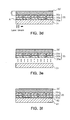
- FIGS. 2A to 2E are sectional views for illustrating a method for manufacturing a nitride based single crystal in accordance with one embodiment of the present invention.
- a nitride based single crystal layer 25 is formed on a preliminary substrate 21.
- the preliminary substrate 21 mainly uses a sapphire substrate.
- the preliminary substrate 21 is not limited thereto, and may use any substrate having a higher band gap than that of a nitride based single crystal.
- the preliminary substrate 21 is made of one material selected from the group consisting of SiC, Si, MgAl 2 O 4 , MgO, LiAlO 2 , and LiGaO 2 .
- the nitride based single crystal layer 25 satisfies the molecular formula of Al x In y Ga (1-x-y) N (here, 0 ⁇ x ⁇ 1, 0 ⁇ y ⁇ 1, and 0 ⁇ x+y ⁇ 1).
- the nitride based single crystal layer 25 is grown on the preliminary substrate 21 using hydride vapor phase epitaxy (HVPE), metal organic chemical vapor deposition (MOCVD), or molecular beam epitaxy (MBE).
- HVPE hydride vapor phase epitaxy
- MOCVD metal organic chemical vapor deposition
- MBE molecular beam epitaxy
- the growing of the nitride based single crystal layer 25 is performed at a high temperature of 900 ⁇ 1,200°C, the grown nitride based single crystal layer 25 is easily exposed to stress generating conditions when the nitride based single crystal layer 25 is cooled to the room temperature.
- a setting adhesive material 26 having flowability is applied to the upper surface of the nitride based single crystal layer 25.
- the setting adhesive material 26 is one selected from the group consisting of a thermosetting resin, an ultraviolet-setting resin, a naturally setting resin, and their mixtures, which can maintain a high adhesive strength with the preliminary substrate 21.
- epoxy resin which has a thermosetting property and a high adhesive strength with the nitride based single crystal layer 25, is used as the setting adhesive material 26.
- This setting adhesive material 26 having flowability is easily supplied to the upper surface of the nitride based single crystal layer 25 by the conventional application method, such as spin coating or hand printing.
- the applied adhesive material 26 is hardened, thereby forming a polymer support layer 26'.
- a proper hardening process may be selected according to the hardening condition of the selected setting adhesive material 26.
- the setting adhesive material 26 is exposed to a proper temperature, thus forming the desired polymer support layer 26'.
- the polymer support layer 26' which contacts the nitride based single crystal layer 25, prevents crack and warpage of the nitride based single crystal layer 25 due to stress applied thereto, and allows the obtained nitride based single crystal layer 25 to be easily handled during or after the process.
- the thickness (t) of the polymer support layer 26' is preferably at least 10 ⁇ m, and more preferably more than 100 ⁇ m in consideration of handling and a post-treatment.
- the thickness (t) of the polymer support layer 26' exceeds 5mm, it is difficult to achieve the uniform thickness (t) of the polymer support layer 26'. Accordingly, preferably, the thickness (t) of the polymer support layer 26' is less than 5mm.
- a laser beam is irradiated onto the lower surface of the preliminary substrate 21, thereby separating the nitride based single crystal layer 25 from the preliminary substrate 21.
- the irradiated laser beam has a wavelength corresponding to a band gap, which is smaller than that of the material of the preliminary substrate 21 and larger than that of the nitride based single crystal layer 25.
- a Nd-YAG laser beam having a wavelength of 355nm is used.
- a region (A) of the preliminary substrate 21, onto which the laser beam is irradiated, is decomposed into nitrogen and metal, as described above.
- the gallium nitride layer is decomposed into metal, i.e., gallium (Ga), and nitrogen (1/2N 2 ).
- the laser beam is irradiated onto the whole area of the lower surface of the preliminary substrate 21 by a scanning method, and decomposes the interface region (A) of the nitride based single crystal layer 25 with the preliminary substrate, thereby separating the nitride based single crystal layer 25 from the preliminary substrate 21.
- the polymer support layer 26' is removed from the nitride based single crystal layer 25.
- the nitride based single crystal layer 25, from which the polymer support layer 26' was removed, is referred to as the nitride based single crystal substrate 25.
- the polymer support layer 26' is easily removed using a proper solvent.
- the easy of removing the polymer support layer 26 is an advantage of the present invention.
- the proper solvent is one selected from the group consisting of various organic solvents and hot water according to the material of the polymer support layer 26'.
- the process for removing the polymer support layer 26' from the nitride based single crystal layer 25 may be omitted, and the polymer support layer 26' may be maintained until the nitride based single crystal substrate 25 is supplied to a final user. That is, the polymer support layer 26' assures the safe handling of the obtained single crystal substrate 25. Since the polymer support layer 26' is easily removed by a simple process, the polymer support layer 26' serves as a support member until the nitride based single crystal substrate 25 is supplied to the final user.
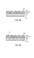
- FIGS. 3A to 3H are sectional views for illustrating a method for manufacturing a nitride based light emitting device in accordance with one embodiment of the present invention. Those skilled in the art will appreciated that the method of FIGS. 2A to 2E can be applied to a process for manufacturing a nitride based light emitting device.
- a first conduction-type nitride based semiconductor layer 35a, an active layer 35b, and a second conduction-type nitride based semiconductor layer 35c are sequentially stacked on a preliminary substrate 31.
- the first conduction-type nitride based semiconductor layer 35a, the active layer 35b, and the second conduction-type nitride based semiconductor layer 35c form a desired nitride based light emitting structure 35.
- the light emitting structure 35 is partially cut into portions having a size corresponding to that of individual light emitting diodes.
- this cutting process is a preliminary cutting process out of various cutting processes.
- Cutting grooves (H) serve to relieve stress generated during the laser lift-off process.
- a setting adhesive material 36 (in FIG. 3C), which will be applied in a subsequent process, fills the cutting grooves (H), and is hardened, thereby forming a polymer support layer 36' (in FIG. 3C) more firmly connected to the nitride based light emitting structure 35.
- the width of the cutting grooves (H), i.e., the cutting width (g), is preferably 10 ⁇ 500 ⁇ m.
- the cutting width (g) is below 10 ⁇ m, it is difficult to fill the cutting grooves (H) with the adhesive material 36, and when the cutting width (g) is above 500 ⁇ m, a loss area of a wafer is excessively increased.
- the setting adhesive material 36 having flowability is applied to the upper surface of the nitride based light emitting structure 35.
- the setting adhesive material 36 has flowability, thus being capable of filling the cutting grooves (H).
- the setting adhesive material 36 is one selected from the group consisting of a thermosetting resin, an ultraviolet-setting resin, a naturally setting resin, and their mixtures, which can maintain a high adhesive strength with the preliminary substrate 31.
- epoxy resin which has a thermosetting property, is used as the setting adhesive material 36.
- This setting adhesive material 36 is easily supplied to the upper surface of the nitride based light emitting structure 35 by the conventional application method, such as spin coating or hand printing.
- the adhesive material 36 is hardened, thereby forming the polymer support layer 36'.
- a proper hardening process may be selected according to the hardening condition of the selected setting adhesive material 36.
- the polymer support layer 36' which contacts the nitride based light emitting structure 35, prevents cracks and warpage of the nitride based light emitting structure 35 due to stress applied thereto, and allows the nitride based light emitting structure 35 to be easily handled during the process.
- the thickness (t) of the polymer support layer 36' is preferably at least 10 ⁇ m, and more preferably more than 100 ⁇ m in consideration of supporting and handling.
- the thickness (t) of the polymer support layer 36' does not exceed 5mm.
- the polymer support layer 36' is formed up to the surfaces of the cutting grooves (H), thus having a higher adhesive strength.
- a laser beam is irradiated onto the lower surface of the preliminary substrate 31, thereby separating the nitride based light emitting structure 35 from the preliminary substrate 31.
- the irradiated laser beam has a wavelength corresponding to a band gap, which is smaller than that of the material of the preliminary substrate 31 and larger than that of a nitride single crystal.
- the thickness (ta) of the non-cut portion of the nitride based light emitting structure 35 is set to a proper value, thereby completely separating the nitride based light emitting structure 35 from the preliminary substrate 31.
- the thickness (ta) of the non-cut portion of the light emitting structure 35 is preferably 5 ⁇ 500nm.
- the separated surface of the light emitting structure 35 is bonded to a permanent substrate 41.
- the permanent substrate 41 mainly uses a silicon substrate.
- the permanent substrate 41 is not limited thereto, and may be a substrate made of one conductive material selected from the group consisting of SiC, ZnO and GaAs. This bonding process is may be performed by thermocompression. In this embodiment, the bonding process is performed using a separate conductive adhesive layer 42.
- the conductive adhesive layer 42 is made of Au-Sn, Sn, Au-Ag, Ag-Cu, or Pb-Cu.
- the stack order of the first conduction-type nitride based semiconductor layer 35a, the active layer 35b, and the second conduction-type nitride based semiconductor layer 35c on the preliminary substrate 31 is also maintained on the permanent substrate 41. It is a technical difference between the method of the present invention and the conventional method disclosed in Korean Patent Registration No. 483049 .
- the polymer support layer 36' is removed from the nitride based light emitting structure 35, and first and second electrodes 44a and 44b are respectively formed on the lower surface of the permanent substrate 31 and the upper surface of the light emitting structure 35.
- the polymer support layer 36' is easily removed using a proper solvent. In this embodiment, although the cutting grooves are filled with the polymer support layer 36', the polymer support layer 36' is easily dissolved in the proper solvent, thus being completely removed.
- the first and second electrodes 44a and 44b are respectively provided to the lower surface of the permanent substrate 31 and the upper surface of the light emitting structure 35, as shown in FIG. 3G.
- n-type nitride based semiconductor layer facilitating formation of Ohmic contact on the upper portion of the light emitting structure 35
- a p-type nitride based semiconductor layer, an active layer, and the n-type nitride based semiconductor layer are sequentially stacked.
- the initial stack order of the layers can be maintained, and thus is equal to the final stack order of the layers.
- the obtained structure is completely divided into individual light emitting diodes 30.
- the light emitting structure 35 and the permanent substrate 41 are completely divided into the light emitting diodes 30 along the partially cutting grooves (H).
- this dividing process may be variously modified.
- the partial cutting process of FIG. 3B is not employed, and the light emitting structure 35 is completely divided into the individual light emitting diodes 30 after the first and second electrodes 44a and 44b are formed.
- the permanent substrate 41 is divided into portions corresponding to the light emitting diodes 30 in this process.
- a method for manufacturing a nitride based light emitting device of the present invention may not employ a conductive permanent substrate.
- the obtained nitride based light emitting device may include a nitride based single crystal structure without a substrate.
- FIGS. 4A to 4E are sectional views for illustrating a method for manufacturing a nitride based light emitting device in accordance with another embodiment of the present invention.
- a first conduction-type nitride based semiconductor layer 55a, an active layer 55b, and a second conduction-type nitride based semiconductor layer 55c are sequentially stacked on a preliminary substrate 51.
- the first conduction-type nitride based semiconductor layer 55a, the active layer 55b, and the second conduction-type nitride based semiconductor layer 55c form a desired nitride based light emitting structure 55.
- the light emitting structure 55 is cut into portions having a size corresponding to that of individual light emitting diodes.
- This cutting process may be a completely cutting process or a preliminary cutting process.
- the cutting process is a preliminary cutting process, in which a portion of the light emitting structure 55 having a designated thickness, which can be removed by a subsequent laser lift-off process, remains.
- cutting grooves serve to relieve stress generated during the laser lift-off process.
- the width of the cutting grooves i.e., the cutting width (g), is preferably 10 ⁇ 500 ⁇ m.
- electrodes 64 are formed on the upper surface of the second conduction-type nitride based semiconductor layer 55c, and a setting adhesive material 56 having flowability is applied to the upper surface of the nitride based light emitting structure 55.
- the electrodes 64 are formed on the nitride based light emitting structure 55 before the setting adhesive material 56 is applied to the nitride based light emitting structure 55. Since the second conduction-type nitride based semiconductor layer 55c is generally a p-type nitride based semiconductor layer, the electrodes 64 having shapes appropriate for formation of Ohmic contact are employed.
- the setting adhesive material 56 has flowability, thus being capable of filling the cutting grooves (H).
- the setting adhesive material 56 is easily supplied to the upper surface of the nitride based light emitting structure 55 by the conventional application method, such as spin coating or hand printing.
- the adhesive material 56 is hardened, thereby forming a polymer support layer 56'.
- a proper hardening process may be selected according to the hardening condition of the selected setting adhesive material 56.
- the polymer support layer 56' which contacts the nitride based light emitting structure 55, prevents cracks and warpage of the nitride based light emitting structure 55 due to stress applied thereto, and allows the nitride based light emitting structure 55 to be easily handled during the process.
- the thickness (t) of the polymer support layer 56' is preferably at least 10 ⁇ m, and more preferably more than 100 ⁇ m in consideration of supporting and handling. Further, so as to uniformly form the polymer support layer 56', preferably, the thickness (t) of the polymer support layer 56' does not exceed 5mm.
- a laser beam is irradiated onto the lower surface of the preliminary substrate 51, thereby separating the nitride based light emitting structure 55 from the preliminary substrate 51.
- the irradiated laser beam has a wavelength corresponding to a band gap, which is smaller than that of the material of the preliminary substrate 51 and larger than that of a nitride based single crystal.
- the non-cut portion of the nitride based light emitting structure 55 is removed by this laser lift-off process, thereby completely separating the light emitting structure 55 from the preliminary substrate 51. This facilitates a subsequent process for dividing the light emitting structure 55 into individual chips.
- the thickness (ta) of the non-cut portion of the light emitting structure 55 is preferably 5 ⁇ 500nm.
- the cut portions of the light emitting structure 55 may be used as light emitting diodes under the condition that the cut portions are not bonded on a permanent substrate.
- any separate electrode need not be formed on the first conduction-type nitride based semiconductor layer 55a. That is, when the first conduction-type nitride based semiconductor layer 55a is an n-type semiconductor layer facilitating formation of Ohmic contact, the cut portions of the light emitting structure 55 are mounted directly on electrode pads of a board, such as a package substrate or a printed circuit board.
- the polymer support layer 56' is easily removed using a proper solvent, such as one of various organic solvents or hot water.
- a proper solvent such as one of various organic solvents or hot water.
- the polymer support layer 56' since the light emitting structure 55 is not supported by a substrate, the polymer support layer 56' has a comparatively large thickness of at least 100 ⁇ m, thereby allowing the individual light emitting diodes to be easily handled.
- the present invention provides a method for manufacturing a nitride based single crystal substrate and a method for manufacturing a nitride based light emitting device, in which a support layer contacting the nitride based single crystal substrate and the nitride based light emitting device is formed by depositing a setting adhesive material having flowability, thereby preventing the generation of cracks and warpage due to stress and being easily handled during or after a process.
Landscapes
- Chemical & Material Sciences (AREA)
- Engineering & Computer Science (AREA)
- Crystallography & Structural Chemistry (AREA)
- Materials Engineering (AREA)
- Metallurgy (AREA)
- Organic Chemistry (AREA)
- Inorganic Chemistry (AREA)
- Led Devices (AREA)
- Recrystallisation Techniques (AREA)
Abstract
Description
- This application claims the benefit of
Korean Patent Application No. 2005-74246 filed on August 12, 2005 - The present invention relates to a method for manufacturing a nitride based single crystal substrate and a method for manufacturing a nitride based semiconductor device, and more particularly to a method for manufacturing a nitride based single crystal substrate and a method for manufacturing a nitride based semiconductor device, which prevent yield reduction due to cracks generated in a laser lift-off process.
- Generally, III-V group nitride based semiconductors emit light of a wide range from visible rays to ultraviolet rays. These nitride based semiconductors are widely used as optical elements for emitting ultraviolet rays and a bluish green color ray.
- In order to apply a nitride based semiconductor to a light emitting device, a technique of growing a high-definition single crystal thin film of the nitride based semiconductor is required. Generally, the nitride based single crystal thin film is grown on a substrate made of a different material, such as a sapphire (Al2O3) substrate or a silicon carbide (SiC) substrate, by a hetero-epitaxy method using metal organic chemical vapor deposition (MOCVD) and molecular beam epitaxy (MBE).
- Although the nitride based single crystal is grown on the sapphire substrate, since a difference of lattice constants between gallium nitride and sapphire is approximately 13% and a difference of thermal expansion coefficients between gallium nitride and sapphire is -34%, stress is generated from an interface between the sapphire substrate and the gallium nitride single crystal. Accordingly, in order to grow a nitride based semiconductor device directly on a nitride based single crystal substrate, a freestanding nitride based single crystal substrate is required.
- As shown in FIG. 1, the freestanding nitride based single crystal substrate is obtained by growing a nitride based
single crystal 15 on apreliminary substrate 11, such as a sapphire substrate, and separating the nitride basedsingle crystal 15 from thepreliminary substrate 11 using a laser lift-off process. The laser lift-off process is performed by decomposing the nitride basedsingle crystal 15 at an interface region with thesapphire substrate 11 into metal by irradiating a laser beam thereonto, and separating the metal from thepreliminary substrate 11 by melting. Here, a portion of the nitride basedsingle crystal 15, onto which the laser beam is irradiated, is decomposed into metal, i.e., gallium (Ga), and nitrogen (1/2N2). - As disclosed in Korean Patent Registration
No. 483049 - However, the preliminary substrate is made of a material different from the nitride based light emitting structure, thus causing warpage and cracks (C) at the interface therebetween due to a difference of lattice constants and a difference of thermal expansion coefficients. Particularly, thermal stress due to the difference of thermal expansion coefficients severely occurs when the nitride based single crystal grown at a high temperature (900~1,200°C) is cooled to the room temperature for the laser lift-off process.
- In order to solve the above problem, as disclosed in
Korean Patent Application No. 2005-0000265 - Accordingly, a method for more simply solving problems caused by stress between a nitride based single crystal or a nitride based light emitting structure and a preliminary substrate made of a material different from the nitride based single crystal or light emitting structure has been required.
- Therefore, the present invention has been made in view of the above problems, and it is an object of the present invention to provide a method for manufacturing a nitride based single crystal substrate, in which a support layer is formed by depositing a setting material having flowability and adhesiveness on a nitride based single crystal layer, thereby preventing the generation of cracks and warpage due to stress and being easily handled.
- It is another object of the present invention to provide a method for manufacturing a nitride based light emitting device, in which a support layer is formed by depositing a setting material having flowability and adhesiveness on the nitride based light emitting device, thereby preventing the generation of cracks and warpage due to stress and being easily handled.
- In accordance with one aspect of the present invention, the above and other objects can be accomplished by the provision of a method for manufacturing a nitride based single crystal substrate comprising forming a nitride based single crystal layer on a preliminary substrate; forming a polymer support layer by applying a setting adhesive material having flowability on the upper surface of the nitride based single crystal layer and hardening the applied adhesive material; and separating the nitride based single crystal layer from the preliminary substrate by irradiating a laser beam onto the lower surface of the preliminary substrate.
- The method may further comprise removing the polymer support layer from the nitride based single crystal layer. The preliminary substrate is mainly made of sapphire, but is not limited thereto. That is, the preliminary substrate may be made of a material having an energy band gap larger than that of the nitride based single crystal layer. Because the used laser beam has a wavelength corresponding to a band gap, which is smaller than that of the preliminary substrate and larger than that of the nitride based single crystal layer. For example, the preliminary substrate is made of one material selected from the group consisting of sapphire, SiC, Si, MgAl2O4, MgO, LiAlO2, and LiGaO2.
- The setting adhesive material may include at least one selected from the group consisting of a thermosetting resin, an ultraviolet-setting resin, and a naturally setting resin, which have a high adhesive strength with the nitride based single crystal layer. Preferably, the setting adhesive material is epoxy resin.
- The applying of the setting adhesive material may be easily performed by spin coating or hand printing. In order to have a sufficient support function, the polymer support layer preferably has a thickness of more than 10µm. In consideration of a subsequent handling process, the polymer support layer more preferably has a thickness of more than 100µm. Further, although the maximum thickness of the polymer support layer is not limited, in order to uniformly form the polymer support layer, the polymer support layer preferably has a thickness not exceeding 5mm.
- In accordance with another aspect of the present invention, there is provided a method for manufacturing a nitride based light emitting device comprising forming a nitride based light emitting structure by sequentially stacking a first conduction-type nitride based semiconductor layer, an active layer, and a second conduction-type nitride based semiconductor layer on a preliminary substrate; forming a polymer support layer by applying a setting adhesive material having flowability on the upper surface of the nitride based light emitting structure and hardening the applied adhesive material; separating the nitride based light emitting structure from the preliminary substrate by irradiating a laser beam onto the lower surface of the preliminary substrate; bonding the light emitting structure to a conductive permanent substrate in such a manner that the separated surface of the light emitting structure serves as a bonding surface; removing the polymer support layer from the light emitting structure; and forming first and second electrodes on the upper surface of the light emitting structure and the lower surface of the permanent substrate, respectively.
- Dividing the light emitting structure into the individual light emitting diodes of the present invention may be variously modified. In one embodiment, the method may further comprise cutting the light emitting structure into portions having a size corresponding to that of desired light emitting diodes, after the forming of the first and second electrodes.
- Further, the method may further comprise partially cutting the light emitting structure into portions having a size corresponding to that of desired light emitting diodes, between the forming of the light emitting structure and the forming of the polymer support layer; and completely cutting the light emitting structure into portions having the size corresponding to that of the desired light emitting diodes, after the forming of the first and second electrodes.
- In another embodiment, the method may further comprise partially cutting the light emitting structure into portions having a size corresponding to that of desired light emitting diodes, between the forming of the light emitting structure and the forming of the polymer support layer, wherein the light emitting structure is divided into individual light emitting diodes by removing the portion of the light emitting structure, which is not cut in the partially cutting of the light emitting structure, in the separating of the light emitting structure from the preliminary substrate. In this case, the portion of the light emitting structure, which is not cut in the partially cutting of the light emitting structure, has a thickness determined by the subsequent process.
- That is, when the separating of the light emitting structure from the preliminary substrate is performed by a laser lift-off process, the portion of the light emitting structure, which is not cut in the partially cutting of the light emitting structure, preferably has a thickness of 5~500nm. On the other hand, when the separating of the light emitting structure from the preliminary substrate is performed by dry or wet etching or lapping/polishing, the portion of the light emitting structure, which is not cut in the partially cutting of the light emitting structure, preferably has a thickness of more than 500nm.
- In case that the light emitting structure is partially or completely cut before the forming of the polymer support layer, the forming of the polymer support layer preferably includes applying the setting adhesive material so that grooves, which are formed in the light emitting structure in the partially cutting of the light emitting structure, are filled with the setting adhesive material. For this reason, the grooves, which are formed in the light emitting structure in the partially cutting of the light emitting structure, preferably have a width of 10~500µm. When the width of the grooves is below 10µm, it is difficult to fill the grooves with the adhesive material, and when the width of the grooves is above 500µm, a loss area of a wafer is excessively increased.
- In accordance with yet another aspect of the present invention, there is provided a method for manufacturing a nitride based light emitting device comprising forming a nitride based light emitting structure by sequentially stacking a first conduction-type nitride based semiconductor layer, an active layer, and a second conduction-type nitride based semiconductor layer on a preliminary substrate; cutting the nitride based light emitting structure into portions having a size corresponding to that of desired light emitting diodes; forming electrodes on the second conduction-type nitride based semiconductor layer; forming a polymer support layer by applying a setting adhesive material having flowability on the upper surface of the nitride based light emitting structure and hardening the applied adhesive material; separating the nitride based light emitting structure from the preliminary substrate by irradiating a laser beam onto the lower surface of the preliminary substrate; and removing the polymer support layer from the light emitting structure.
- The above and other objects, features and other advantages of the present invention will be more clearly understood from the following detailed description taken in conjunction with the accompanying drawings, in which:
- FIG. 1 is a schematic view for illustrating a conventional laser lift-off process for separating nitride based single crystal;
- FIGS. 2A to 2E are sectional views for illustrating a method for manufacturing a nitride based single crystal in accordance with one embodiment of the present invention;
- FIGS. 3A to 3H are sectional views for illustrating a method for manufacturing a nitride based light emitting device in accordance with one embodiment of the present invention; and
- FIGS. 4A to 4E are sectional views for illustrating a method for manufacturing a nitride based light emitting device in accordance with another embodiment of the present invention.
- Now, preferred embodiments of the present invention will be described in detail with reference to the annexed drawings.
- FIGS. 2A to 2E are sectional views for illustrating a method for manufacturing a nitride based single crystal in accordance with one embodiment of the present invention.
- First, as shown in FIG. 2A, a nitride based
single crystal layer 25 is formed on apreliminary substrate 21. Thepreliminary substrate 21 mainly uses a sapphire substrate. However, thepreliminary substrate 21 is not limited thereto, and may use any substrate having a higher band gap than that of a nitride based single crystal. For example, thepreliminary substrate 21 is made of one material selected from the group consisting of SiC, Si, MgAl2O4, MgO, LiAlO2, and LiGaO2. The nitride basedsingle crystal layer 25 satisfies the molecular formula of AlxInyGa(1-x-y)N (here, 0≤x≤1, 0≤y≤1, and 0≤x+y≤1). The nitride basedsingle crystal layer 25 is grown on thepreliminary substrate 21 using hydride vapor phase epitaxy (HVPE), metal organic chemical vapor deposition (MOCVD), or molecular beam epitaxy (MBE). Since the growing of the nitride basedsingle crystal layer 25 is performed at a high temperature of 900~1,200°C, the grown nitride basedsingle crystal layer 25 is easily exposed to stress generating conditions when the nitride basedsingle crystal layer 25 is cooled to the room temperature. - Thereafter, as shown in FIG. 2B, a setting
adhesive material 26 having flowability is applied to the upper surface of the nitride basedsingle crystal layer 25. Any material, which has flowability and is hardened under a predetermined condition so as to form a support structure, may be used as the settingadhesive material 26 of the present invention. For example, the settingadhesive material 26 is one selected from the group consisting of a thermosetting resin, an ultraviolet-setting resin, a naturally setting resin, and their mixtures, which can maintain a high adhesive strength with thepreliminary substrate 21. Preferably, epoxy resin, which has a thermosetting property and a high adhesive strength with the nitride basedsingle crystal layer 25, is used as the settingadhesive material 26. This settingadhesive material 26 having flowability is easily supplied to the upper surface of the nitride basedsingle crystal layer 25 by the conventional application method, such as spin coating or hand printing. - Thereafter, as shown in FIG. 2C, the applied
adhesive material 26 is hardened, thereby forming a polymer support layer 26'. Here, a proper hardening process may be selected according to the hardening condition of the selected settingadhesive material 26. For example, when epoxy resin is used as the settingadhesive material 26, the settingadhesive material 26 is exposed to a proper temperature, thus forming the desired polymer support layer 26'. The polymer support layer 26', which contacts the nitride basedsingle crystal layer 25, prevents crack and warpage of the nitride basedsingle crystal layer 25 due to stress applied thereto, and allows the obtained nitride basedsingle crystal layer 25 to be easily handled during or after the process. For this reason, the thickness (t) of the polymer support layer 26' is preferably at least 10µm, and more preferably more than 100µm in consideration of handling and a post-treatment. When the thickness (t) of the polymer support layer 26' exceeds 5mm, it is difficult to achieve the uniform thickness (t) of the polymer support layer 26'. Accordingly, preferably, the thickness (t) of the polymer support layer 26' is less than 5mm. - Thereafter, as shown in FIG. 2D, a laser beam is irradiated onto the lower surface of the
preliminary substrate 21, thereby separating the nitride basedsingle crystal layer 25 from thepreliminary substrate 21. The irradiated laser beam has a wavelength corresponding to a band gap, which is smaller than that of the material of thepreliminary substrate 21 and larger than that of the nitride basedsingle crystal layer 25. For example, when a sapphire substrate is used as thepreliminary substrate 21, a Nd-YAG laser beam having a wavelength of 355nm is used. A region (A) of thepreliminary substrate 21, onto which the laser beam is irradiated, is decomposed into nitrogen and metal, as described above. For example, when a gallium nitride (GaN) layer is formed, the gallium nitride layer is decomposed into metal, i.e., gallium (Ga), and nitrogen (1/2N2). The laser beam is irradiated onto the whole area of the lower surface of thepreliminary substrate 21 by a scanning method, and decomposes the interface region (A) of the nitride basedsingle crystal layer 25 with the preliminary substrate, thereby separating the nitride basedsingle crystal layer 25 from thepreliminary substrate 21. - Finally, as shown in FIG. 2E, the polymer support layer 26' is removed from the nitride based
single crystal layer 25. The nitride basedsingle crystal layer 25, from which the polymer support layer 26' was removed, is referred to as the nitride basedsingle crystal substrate 25. The polymer support layer 26' is easily removed using a proper solvent. The easy of removing thepolymer support layer 26 is an advantage of the present invention. The proper solvent is one selected from the group consisting of various organic solvents and hot water according to the material of the polymer support layer 26'. If necessary, the process for removing the polymer support layer 26' from the nitride basedsingle crystal layer 25 may be omitted, and the polymer support layer 26' may be maintained until the nitride basedsingle crystal substrate 25 is supplied to a final user. That is, the polymer support layer 26' assures the safe handling of the obtainedsingle crystal substrate 25. Since the polymer support layer 26' is easily removed by a simple process, the polymer support layer 26' serves as a support member until the nitride basedsingle crystal substrate 25 is supplied to the final user. - FIGS. 3A to 3H are sectional views for illustrating a method for manufacturing a nitride based light emitting device in accordance with one embodiment of the present invention. Those skilled in the art will appreciated that the method of FIGS. 2A to 2E can be applied to a process for manufacturing a nitride based light emitting device.
- First, as shown in FIG. 3A, a first conduction-type nitride based
semiconductor layer 35a, anactive layer 35b, and a second conduction-type nitride basedsemiconductor layer 35c are sequentially stacked on apreliminary substrate 31. The first conduction-type nitride basedsemiconductor layer 35a, theactive layer 35b, and the second conduction-type nitride basedsemiconductor layer 35c form a desired nitride basedlight emitting structure 35. - Thereafter, as shown in FIG. 3B, the
light emitting structure 35 is partially cut into portions having a size corresponding to that of individual light emitting diodes. In this embodiment of the present invention, this cutting process is a preliminary cutting process out of various cutting processes. Cutting grooves (H) serve to relieve stress generated during the laser lift-off process. Further, a setting adhesive material 36 (in FIG. 3C), which will be applied in a subsequent process, fills the cutting grooves (H), and is hardened, thereby forming a polymer support layer 36' (in FIG. 3C) more firmly connected to the nitride basedlight emitting structure 35. For this reason, the width of the cutting grooves (H), i.e., the cutting width (g), is preferably 10~500µm. When the cutting width (g) is below 10µm, it is difficult to fill the cutting grooves (H) with theadhesive material 36, and when the cutting width (g) is above 500µm, a loss area of a wafer is excessively increased. - Thereafter, as shown in FIG. 3C, the setting
adhesive material 36 having flowability is applied to the upper surface of the nitride basedlight emitting structure 35. As described above, the settingadhesive material 36 has flowability, thus being capable of filling the cutting grooves (H). The settingadhesive material 36 is one selected from the group consisting of a thermosetting resin, an ultraviolet-setting resin, a naturally setting resin, and their mixtures, which can maintain a high adhesive strength with thepreliminary substrate 31. Preferably, epoxy resin, which has a thermosetting property, is used as the settingadhesive material 36. This settingadhesive material 36 is easily supplied to the upper surface of the nitride basedlight emitting structure 35 by the conventional application method, such as spin coating or hand printing. - Thereafter, as shown in FIG. 3D, the
adhesive material 36 is hardened, thereby forming the polymer support layer 36'. Here, a proper hardening process may be selected according to the hardening condition of the selected settingadhesive material 36. The polymer support layer 36', which contacts the nitride basedlight emitting structure 35, prevents cracks and warpage of the nitride basedlight emitting structure 35 due to stress applied thereto, and allows the nitride basedlight emitting structure 35 to be easily handled during the process. For this reason, the thickness (t) of the polymer support layer 36' is preferably at least 10µm, and more preferably more than 100µm in consideration of supporting and handling. Further, so as to uniformly form the polymer support layer 36', preferably, the thickness (t) of the polymer support layer 36' does not exceed 5mm. In this embodiment, the polymer support layer 36' is formed up to the surfaces of the cutting grooves (H), thus having a higher adhesive strength. - Thereafter, as shown in FIG. 3E, a laser beam is irradiated onto the lower surface of the
preliminary substrate 31, thereby separating the nitride basedlight emitting structure 35 from thepreliminary substrate 31. As described above, the irradiated laser beam has a wavelength corresponding to a band gap, which is smaller than that of the material of thepreliminary substrate 31 and larger than that of a nitride single crystal. Further, in this embodiment, when the partial cutting process, as shown in FIG. 3B, is employed, the thickness (ta) of the non-cut portion of the nitride basedlight emitting structure 35 is set to a proper value, thereby completely separating the nitride basedlight emitting structure 35 from thepreliminary substrate 31. This facilitates a subsequent process for dividing the nitride basedlight emitting structure 35 into individual chips. That is, since the nitride basedlight emitting structure 35 having a high hardness is not cut during the subsequent individual chip dividing process, the subsequent individual chip separating process is more easily performed. As described above, in order to completely separate the nitride basedlight emitting structure 35 from thepreliminary substrate 31 in the laser lift-off process, the thickness (ta) of the non-cut portion of thelight emitting structure 35 is preferably 5~500nm. - Thereafter, as shown in FIG. 3F, in order to use the separated surface of the light emitting structure 35 (i.e., the lower surface of the first conduction-type nitride based
semiconductor layer 35a) as a bonding surface, the separated surface of thelight emitting structure 35 is bonded to apermanent substrate 41. Thepermanent substrate 41 mainly uses a silicon substrate. However, thepermanent substrate 41 is not limited thereto, and may be a substrate made of one conductive material selected from the group consisting of SiC, ZnO and GaAs. This bonding process is may be performed by thermocompression. In this embodiment, the bonding process is performed using a separate conductiveadhesive layer 42. The conductiveadhesive layer 42 is made of Au-Sn, Sn, Au-Ag, Ag-Cu, or Pb-Cu. In accordance with the present invention, the stack order of the first conduction-type nitride basedsemiconductor layer 35a, theactive layer 35b, and the second conduction-type nitride basedsemiconductor layer 35c on thepreliminary substrate 31 is also maintained on thepermanent substrate 41. It is a technical difference between the method of the present invention and the conventional method disclosed in Korean Patent RegistrationNo. 483049 - Thereafter, as shown in FIG. 3G, the polymer support layer 36' is removed from the nitride based
light emitting structure 35, and first andsecond electrodes permanent substrate 31 and the upper surface of thelight emitting structure 35. The polymer support layer 36' is easily removed using a proper solvent. In this embodiment, although the cutting grooves are filled with the polymer support layer 36', the polymer support layer 36' is easily dissolved in the proper solvent, thus being completely removed. After the removal of the polymer support layer 36', the first andsecond electrodes permanent substrate 31 and the upper surface of thelight emitting structure 35, as shown in FIG. 3G. In order to dispose an n-type nitride based semiconductor layer facilitating formation of Ohmic contact on the upper portion of thelight emitting structure 35, in the process of FIG. 3A, a p-type nitride based semiconductor layer, an active layer, and the n-type nitride based semiconductor layer are sequentially stacked. In this embodiment of the present invention, the initial stack order of the layers can be maintained, and thus is equal to the final stack order of the layers. - Finally, as shown in FIG. 3H, the obtained structure is completely divided into individual
light emitting diodes 30. In this embodiment, thelight emitting structure 35 and thepermanent substrate 41 are completely divided into thelight emitting diodes 30 along the partially cutting grooves (H). However, this dividing process may be variously modified. For example, the partial cutting process of FIG. 3B is not employed, and thelight emitting structure 35 is completely divided into the individuallight emitting diodes 30 after the first andsecond electrodes light emitting structure 35 is divided into portions corresponding to thelight emitting diode 30 in the process of FIG. 3B or the non-cut portion of thelight emitting structure 35 is removed in the laser lift-off process of FIG. 3D, thepermanent substrate 41 is divided into portions corresponding to thelight emitting diodes 30 in this process. - A method for manufacturing a nitride based light emitting device of the present invention may not employ a conductive permanent substrate. In this case, the obtained nitride based light emitting device may include a nitride based single crystal structure without a substrate.
- FIGS. 4A to 4E are sectional views for illustrating a method for manufacturing a nitride based light emitting device in accordance with another embodiment of the present invention.
- First, as shown in FIG. 4A, a first conduction-type nitride based
semiconductor layer 55a, anactive layer 55b, and a second conduction-type nitride basedsemiconductor layer 55c are sequentially stacked on apreliminary substrate 51. The first conduction-type nitride basedsemiconductor layer 55a, theactive layer 55b, and the second conduction-type nitride basedsemiconductor layer 55c form a desired nitride basedlight emitting structure 55. - Thereafter, as shown in FIG. 4B, the
light emitting structure 55 is cut into portions having a size corresponding to that of individual light emitting diodes. This cutting process may be a completely cutting process or a preliminary cutting process. In this embodiment, the cutting process is a preliminary cutting process, in which a portion of thelight emitting structure 55 having a designated thickness, which can be removed by a subsequent laser lift-off process, remains. Here, cutting grooves serve to relieve stress generated during the laser lift-off process. Preferably, the width of the cutting grooves, i.e., the cutting width (g), is preferably 10~500µm. - Thereafter, as shown in FIG. 4C,
electrodes 64 are formed on the upper surface of the second conduction-type nitride basedsemiconductor layer 55c, and a settingadhesive material 56 having flowability is applied to the upper surface of the nitride basedlight emitting structure 55. In this embodiment, theelectrodes 64 are formed on the nitride basedlight emitting structure 55 before the settingadhesive material 56 is applied to the nitride basedlight emitting structure 55. Since the second conduction-type nitride basedsemiconductor layer 55c is generally a p-type nitride based semiconductor layer, theelectrodes 64 having shapes appropriate for formation of Ohmic contact are employed. As described above, the settingadhesive material 56 has flowability, thus being capable of filling the cutting grooves (H). The settingadhesive material 56 is easily supplied to the upper surface of the nitride basedlight emitting structure 55 by the conventional application method, such as spin coating or hand printing. - Thereafter, as shown in FIG. 4D, the
adhesive material 56 is hardened, thereby forming a polymer support layer 56'. Here, a proper hardening process may be selected according to the hardening condition of the selected settingadhesive material 56. The polymer support layer 56', which contacts the nitride basedlight emitting structure 55, prevents cracks and warpage of the nitride basedlight emitting structure 55 due to stress applied thereto, and allows the nitride basedlight emitting structure 55 to be easily handled during the process. For this reason, the thickness (t) of the polymer support layer 56' is preferably at least 10µm, and more preferably more than 100µm in consideration of supporting and handling. Further, so as to uniformly form the polymer support layer 56', preferably, the thickness (t) of the polymer support layer 56' does not exceed 5mm. - Thereafter, as shown in FIG. 4E, a laser beam is irradiated onto the lower surface of the
preliminary substrate 51, thereby separating the nitride basedlight emitting structure 55 from thepreliminary substrate 51. As described above, the irradiated laser beam has a wavelength corresponding to a band gap, which is smaller than that of the material of thepreliminary substrate 51 and larger than that of a nitride based single crystal. Further, in this embodiment, the non-cut portion of the nitride basedlight emitting structure 55 is removed by this laser lift-off process, thereby completely separating thelight emitting structure 55 from thepreliminary substrate 51. This facilitates a subsequent process for dividing thelight emitting structure 55 into individual chips. As described above, in order to completely separate the nitride basedlight emitting structure 55 from thepreliminary substrate 51 in the laser lift-off process, the thickness (ta) of the non-cut portion of thelight emitting structure 55 is preferably 5~500nm. - The cut portions of the
light emitting structure 55 may be used as light emitting diodes under the condition that the cut portions are not bonded on a permanent substrate. In this case, any separate electrode need not be formed on the first conduction-type nitride basedsemiconductor layer 55a. That is, when the first conduction-type nitride basedsemiconductor layer 55a is an n-type semiconductor layer facilitating formation of Ohmic contact, the cut portions of thelight emitting structure 55 are mounted directly on electrode pads of a board, such as a package substrate or a printed circuit board. - The polymer support layer 56' is easily removed using a proper solvent, such as one of various organic solvents or hot water. In this embodiment, since the
light emitting structure 55 is not supported by a substrate, the polymer support layer 56' has a comparatively large thickness of at least 100µm, thereby allowing the individual light emitting diodes to be easily handled. - As apparent from the above description, the present invention provides a method for manufacturing a nitride based single crystal substrate and a method for manufacturing a nitride based light emitting device, in which a support layer contacting the nitride based single crystal substrate and the nitride based light emitting device is formed by depositing a setting adhesive material having flowability, thereby preventing the generation of cracks and warpage due to stress and being easily handled during or after a process.
- Although the preferred embodiments of the present invention have been disclosed for illustrative purposes, those skilled in the art will appreciate that various modifications, additions and substitutions are possible, without departing from the scope and spirit of the invention as disclosed in the accompanying claims.
Claims (33)
- A method for manufacturing a nitride based single crystal substrate comprising:forming a nitride based single crystal layer on a preliminary substrate;forming a polymer support layer by applying a setting adhesive material having flowability on the upper surface of the nitride based single crystal layer and hardening the applied adhesive material; andseparating the nitride based single crystal layer from the preliminary substrate by irradiating a laser beam onto the lower surface of the preliminary substrate.
- The method according to claim 1, further comprising removing the polymer support layer from the nitride based single crystal layer.
- The method according to claim 1, wherein the preliminary substrate is made of a material having an energy band gap larger than that of the nitride based single crystal layer.
- The method according to claim 3, wherein the preliminary substrate is made of one material selected from the group consisting of sapphire, SiC, Si, MgAl2O4, MgO, LiAlO2, and LiGaO2.
- The method according to claim 1, wherein the setting adhesive material includes at least one selected from the group consisting of a thermosetting resin, an ultraviolet-setting resin, and a naturally setting resin, which have a high adhesive strength with the nitride based single crystal layer.
- The method according to claim 5, wherein the setting adhesive material is epoxy resin.
- The method according to claim 1, wherein the applying of the setting adhesive material is performed by spin coating or hand printing.
- The method according to claim 1, wherein the polymer support layer has a thickness of 0.01~5mm.
- A method for manufacturing a nitride based light emitting device comprising:forming a nitride based light emitting structure by sequentially stacking a first conduction-type nitride based semiconductor layer, an active layer, and a second conduction-type nitride based semiconductor layer on a preliminary substrate;forming a polymer support layer by applying a setting adhesive material having flowability on the upper surface of the nitride based light emitting structure and hardening the applied adhesive material;separating the nitride based light emitting structure from the preliminary substrate by irradiating a laser beam onto the lower surface of the preliminary substrate;bonding the light emitting structure to a conductive permanent substrate in such a manner that the separated surface of the light emitting structure serves as a bonding surface;removing the polymer support layer from the light emitting structure; andforming first and second electrodes on the upper surface of the light emitting structure and the lower surface of the permanent substrate, respectively.
- The method according to claim 9, further comprising cutting the light emitting structure into portions having a size corresponding to that of desired light emitting diodes, after the forming of the first and second electrodes.
- The method according to claim 9, further comprising:partially cutting the light emitting structure into portions having a size corresponding to that of the desired light emitting diodes, between the forming of the light emitting structure and the forming of the polymer support layer; andcompletely cutting the light emitting structure into portions having the size corresponding to that of desired light emitting diodes, after the forming of the first and second electrodes.
- The method according to claim 9, further comprising partially cutting the light emitting structure into portions having a size corresponding to that of desired light emitting diodes, between the forming of the light emitting structure and the forming of the polymer support layer,
wherein the light emitting structure is divided into individual light emitting diodes by removing a portion of the light emitting structure, which is not cut in the partially cutting of the light emitting structure, in the separating of the light emitting structure from the preliminary substrate. - The method according to claim 12, wherein a portion of the light emitting structure, which is not cut in the partially cutting of the light emitting structure, has a thickness of 5~500nm.
- The method according to claim 11, wherein the forming of the polymer support layer includes applying the setting adhesive material so that grooves, which are formed in the light emitting structure in the partially cutting of the light emitting structure, are filled with the setting adhesive material.
- The method according to claim 11, wherein grooves, which are formed in the light emitting structure in the partially cutting of the light emitting structure, have a width of 10~500µm.
- The method according to claim 9, wherein the preliminary substrate is made of a material having an energy band gap larger than that of the first conduction-type nitride based semiconductor layer.
- The method according to claim 16, wherein the preliminary substrate is made of one material selected from the group consisting of sapphire, SiC, Si, MgAl2O4, MgO, LiAlO2, and LiGaO2.
- The method according to claim 9, wherein the setting adhesive material includes at least one selected from the group consisting of a thermosetting resin, an ultraviolet-setting resin, and a naturally setting resin, which have a high adhesive strength with the nitride based light emitting structure.
- The method according to claim 18, wherein the setting adhesive material is epoxy resin.
- The method according to claim 9, wherein the applying of the setting adhesive material is performed by spin coating or hand printing.
- The method according to claim 9, wherein the polymer support layer has a thickness of 0.01~5mm.
- The method according to claim 9, wherein the first conduction-type and second conduction-type nitride based semiconductor layers are p-type and n-type nitride based semiconductor layers, respectively.
- A method for manufacturing a nitride based light emitting device comprising:forming a nitride based light emitting structure by sequentially stacking a first conduction-type nitride based semiconductor layer, an active layer, and a second conduction-type nitride based semiconductor layer on a preliminary substrate;cutting the nitride based light emitting structure into portions having a size corresponding to that of desired light emitting diodes;forming electrodes on the second conduction-type nitride based semiconductor layer;forming a polymer support layer by applying a setting adhesive material having flowability on the upper surface of the nitride based light emitting structure and hardening the applied adhesive material;separating the nitride based light emitting structure from the preliminary substrate by irradiating a laser beam onto the lower surface of the preliminary substrate; andremoving the polymer support layer from the light emitting structure.
- The method according to claim 23, wherein:in the cutting of the light emitting structure, the light emitting structure is partially cut into portions having the size corresponding to that of the desired light emitting diodes; andthe light emitting structure is divided into individual light emitting diodes by removing a portion of the light emitting structure, which is not cut in the partially cutting of the light emitting structure, in the separating of the light emitting structure from the preliminary substrate.
- The method according to claim 23, wherein a portion of the light emitting structure, which is not cut in the partially cutting of the light emitting structure, have a thickness of 5~500nm.
- The method according to claim 24, wherein the forming of the polymer support layer includes applying the setting adhesive material so that grooves, which are formed in the light emitting structure in the partially cutting of the light emitting structure, are filled with the setting adhesive material.
- The method according to claim 24, wherein grooves, which are formed in the light emitting structure in the partially cutting of the light emitting structure, has a width of 10~50µm.
- The method according to claim 23, wherein the preliminary substrate is made of a material having an energy band gap larger than that of the first conduction-type nitride based semiconductor layer.
- The method according to claim 28, wherein the preliminary substrate is made of one material selected from the group consisting of sapphire, SiC, Si, MgAl2O4, MgO, LiAlO2, and LiGaO2.
- The method according to claim 23, wherein the setting adhesive material includes at least one selected from the group consisting of a thermosetting resin, an ultraviolet-setting resin, and a naturally setting resin, which have a high adhesive strength with the nitride based light emitting structure.
- The method according to claim 30, wherein the setting adhesive material is epoxy resin.
- The method according to claim 23, wherein the applying of the setting adhesive material is performed by spin coating or hand printing.
- The method according to claim 23, wherein the polymer support layer has a thickness of 0.01~5mm.
Applications Claiming Priority (1)
| Application Number | Priority Date | Filing Date | Title |
|---|---|---|---|
| KR1020050074246A KR100632004B1 (en) | 2005-08-12 | 2005-08-12 | Nitride single crystal substrate manufacturing method and nitride semiconductor light emitting device manufacturing method |
Publications (3)
| Publication Number | Publication Date |
|---|---|
| EP1753018A2 true EP1753018A2 (en) | 2007-02-14 |
| EP1753018A3 EP1753018A3 (en) | 2010-03-31 |
| EP1753018B1 EP1753018B1 (en) | 2012-09-12 |
Family
ID=37467520
Family Applications (1)
| Application Number | Title | Priority Date | Filing Date |
|---|---|---|---|
| EP06253864A Active EP1753018B1 (en) | 2005-08-12 | 2006-07-24 | Method for manufacturing nitride based single crystal substrate and method for manufacturing nitride based semiconductor device |
Country Status (4)
| Country | Link |
|---|---|
| US (2) | US8932891B2 (en) |
| EP (1) | EP1753018B1 (en) |
| JP (1) | JP5273423B2 (en) |
| KR (1) | KR100632004B1 (en) |
Cited By (2)
| Publication number | Priority date | Publication date | Assignee | Title |
|---|---|---|---|---|
| EP2063469A2 (en) | 2007-11-23 | 2009-05-27 | Samsung Electro-Mechanics Co., Ltd. | Method of manufacturing vertical light emitting diode |
| EP2680324A1 (en) * | 2012-06-28 | 2014-01-01 | Nitto Denko Corporation | Method of manufacturing a LED |
Families Citing this family (16)
| Publication number | Priority date | Publication date | Assignee | Title |
|---|---|---|---|---|
| KR100706951B1 (en) * | 2005-08-17 | 2007-04-12 | 삼성전기주식회사 | Method for manufacturing vertical structure gallium nitride based LED device |
| KR100752721B1 (en) | 2006-07-12 | 2007-08-29 | 삼성전기주식회사 | Method for manufacturing vertical structure gallium nitride based LED device |
| US8680586B2 (en) * | 2007-01-05 | 2014-03-25 | Rohm Co., Ltd. | Semiconductor light emitting device including GaAs substrate and method for manufacturing the same |
| WO2011069242A1 (en) * | 2009-12-09 | 2011-06-16 | Cooledge Lighting Inc. | Semiconductor dice transfer-enabling apparatus and method for manufacturing transfer-enabling apparatus |
| US20110151588A1 (en) * | 2009-12-17 | 2011-06-23 | Cooledge Lighting, Inc. | Method and magnetic transfer stamp for transferring semiconductor dice using magnetic transfer printing techniques |
| US8334152B2 (en) | 2009-12-18 | 2012-12-18 | Cooledge Lighting, Inc. | Method of manufacturing transferable elements incorporating radiation enabled lift off for allowing transfer from host substrate |
| EP2618363A1 (en) * | 2010-09-16 | 2013-07-24 | Sumitomo Electric Industries, Ltd. | Production method for semiconductor device |
| KR101679397B1 (en) * | 2010-09-24 | 2016-11-25 | 서울바이오시스 주식회사 | Method for fabricating vertical light emitting device |
| KR101035998B1 (en) | 2010-11-18 | 2011-05-23 | 한빔 주식회사 | Vertical LED Manufacturing Method |
| US9165895B2 (en) * | 2011-11-07 | 2015-10-20 | Infineon Technologies Ag | Method for separating a plurality of dies and a processing device for separating a plurality of dies |
| US9847445B2 (en) * | 2012-04-05 | 2017-12-19 | Koninklijke Philips N.V. | LED thin-film device partial singulation prior to substrate thinning or removal |
| JP5982179B2 (en) | 2012-05-28 | 2016-08-31 | 株式会社東芝 | Semiconductor light emitting device and manufacturing method thereof |
| WO2016100657A2 (en) * | 2014-12-19 | 2016-06-23 | Glo Ab | Method of making a light emitting diode array on a backplane |
| EP4170734A4 (en) | 2020-06-18 | 2024-06-19 | Nichia Corporation | METHOD FOR MANUFACTURING IMAGE DISPLAY DEVICE, AND IMAGE DISPLAY DEVICE |
| FR3144532A1 (en) * | 2022-12-28 | 2024-07-05 | Aledia | METHOD FOR MANUFACTURING AN ELECTRONIC DEVICE |
| KR102938780B1 (en) | 2024-02-13 | 2026-03-16 | 주식회사 글로벌테크놀로지 | Light emitting driving device package apparatus, its manufacturing method and wafer for bonding |
Family Cites Families (17)
| Publication number | Priority date | Publication date | Assignee | Title |
|---|---|---|---|---|
| US4882245A (en) * | 1985-10-28 | 1989-11-21 | International Business Machines Corporation | Photoresist composition and printed circuit boards and packages made therewith |
| JP2950106B2 (en) | 1993-07-14 | 1999-09-20 | 松下電器産業株式会社 | Method for manufacturing optical element package |
| US6071795A (en) * | 1998-01-23 | 2000-06-06 | The Regents Of The University Of California | Separation of thin films from transparent substrates by selective optical processing |
| JP2003162231A (en) | 2001-11-26 | 2003-06-06 | Sony Corp | Element manufacturing method, element arranging method, and image display apparatus manufacturing method |
| JP4242599B2 (en) | 2002-04-08 | 2009-03-25 | パナソニック株式会社 | Method for manufacturing nitride semiconductor device and method for manufacturing nitride semiconductor substrate |
| US8294172B2 (en) * | 2002-04-09 | 2012-10-23 | Lg Electronics Inc. | Method of fabricating vertical devices using a metal support film |
| JP3962282B2 (en) * | 2002-05-23 | 2007-08-22 | 松下電器産業株式会社 | Manufacturing method of semiconductor device |
| JP4360071B2 (en) | 2002-05-24 | 2009-11-11 | 日亜化学工業株式会社 | Manufacturing method of nitride semiconductor laser device |
| US20040140474A1 (en) * | 2002-06-25 | 2004-07-22 | Matsushita Electric Industrial Co., Ltd. | Semiconductor light-emitting device, method for fabricating the same and method for bonding the same |
| KR100483049B1 (en) | 2003-06-03 | 2005-04-15 | 삼성전기주식회사 | A METHOD OF PRODUCING VERTICAL GaN LIGHT EMITTING DIODES |
| JP5142523B2 (en) * | 2003-06-04 | 2013-02-13 | チェオル ユー,ミュング | Vertical structure composite semiconductor device |
| KR20050000265A (en) | 2003-06-23 | 2005-01-03 | 나노바이오주식회사 | Aqueous Composite Fertilizer containing Nano Silver-Allicin and its Manufacturing Process |
| JP4241457B2 (en) | 2003-06-26 | 2009-03-18 | 富士ゼロックス株式会社 | Manufacturing method of light emitting element with lens |
| JP2005056957A (en) | 2003-07-31 | 2005-03-03 | Shin Etsu Handotai Co Ltd | Method of manufacturing light emitting element and temporary supporting laminated body |
| JP2005079385A (en) | 2003-09-01 | 2005-03-24 | Toshiba Corp | Optical semiconductor device and optical signal input / output device |
| JP4428511B2 (en) | 2004-01-22 | 2010-03-10 | 日本化薬株式会社 | Modified epoxy resin, epoxy resin composition containing the same, and cured product thereof |
| KR100616656B1 (en) * | 2005-01-03 | 2006-08-28 | 삼성전기주식회사 | Method and apparatus for manufacturing gallium nitride based single crystal substrate |
-
2005
- 2005-08-12 KR KR1020050074246A patent/KR100632004B1/en not_active Expired - Fee Related
-
2006
- 2006-07-24 EP EP06253864A patent/EP1753018B1/en active Active
- 2006-07-25 US US11/492,009 patent/US8932891B2/en active Active
- 2006-08-02 JP JP2006211250A patent/JP5273423B2/en active Active
-
2010
- 2010-07-26 US US12/843,522 patent/US20100291719A1/en not_active Abandoned
Non-Patent Citations (1)
| Title |
|---|
| None |
Cited By (3)
| Publication number | Priority date | Publication date | Assignee | Title |
|---|---|---|---|---|
| EP2063469A2 (en) | 2007-11-23 | 2009-05-27 | Samsung Electro-Mechanics Co., Ltd. | Method of manufacturing vertical light emitting diode |
| EP2063469A3 (en) * | 2007-11-23 | 2013-03-27 | Samsung Electronics Co., Ltd. | Method of manufacturing vertical light emitting diode |
| EP2680324A1 (en) * | 2012-06-28 | 2014-01-01 | Nitto Denko Corporation | Method of manufacturing a LED |
Also Published As
| Publication number | Publication date |
|---|---|
| EP1753018B1 (en) | 2012-09-12 |
| US20070082486A1 (en) | 2007-04-12 |
| US8932891B2 (en) | 2015-01-13 |
| JP2007053357A (en) | 2007-03-01 |
| JP5273423B2 (en) | 2013-08-28 |
| KR100632004B1 (en) | 2006-10-09 |
| EP1753018A3 (en) | 2010-03-31 |
| US20100291719A1 (en) | 2010-11-18 |
Similar Documents
| Publication | Publication Date | Title |
|---|---|---|
| US20100291719A1 (en) | Method for manufacturing nitride based single crystal substrate and method for manufacturing nitride based semiconductor device | |
| US10586891B2 (en) | Light emitting device with improved extraction efficiency | |
| CN100492610C (en) | Method for production of semiconductor chips | |
| EP2206165B1 (en) | Robust light emitting diode structure with removed substrate and added optical element, method of manufacturing the same | |
| US10510577B2 (en) | Lift off process for chip scale package solid state devices on engineered substrate | |
| EP2063469B1 (en) | Method of manufacturing vertical light emitting diode | |
| US9324926B2 (en) | Wavelength converted light emitting device | |
| US8133803B2 (en) | Method for fabricating semiconductor substrates and semiconductor devices | |
| WO2012059844A1 (en) | Method of forming a composite substrate. | |
| US7892873B2 (en) | Fabrication method of nitride-based semiconductor device | |
| JP2009117583A (en) | Method of manufacturing nitride semiconductor element, nitride semiconductor crystal growth substrate, crystal growth substrate holding board, and adhesive material | |
| US7446346B2 (en) | Semiconductor substrate for optoelectronic components and method for fabricating it | |
| KR20130112903A (en) | Iii-nitride layer grown on a substrate | |
| US20090068776A1 (en) | Method for fabricating semiconductor substrate for optoelectronic components |
Legal Events
| Date | Code | Title | Description |
|---|---|---|---|
| PUAI | Public reference made under article 153(3) epc to a published international application that has entered the european phase |
Free format text: ORIGINAL CODE: 0009012 |
|
| AK | Designated contracting states |
Kind code of ref document: A2 Designated state(s): AT BE BG CH CY CZ DE DK EE ES FI FR GB GR HU IE IS IT LI LT LU LV MC NL PL PT RO SE SI SK TR |
|
| AX | Request for extension of the european patent |
Extension state: AL BA HR MK YU |
|
| PUAL | Search report despatched |
Free format text: ORIGINAL CODE: 0009013 |
|
| AK | Designated contracting states |
Kind code of ref document: A3 Designated state(s): AT BE BG CH CY CZ DE DK EE ES FI FR GB GR HU IE IS IT LI LT LU LV MC NL PL PT RO SE SI SK TR |
|
| AX | Request for extension of the european patent |
Extension state: AL BA HR MK RS |
|
| RAP1 | Party data changed (applicant data changed or rights of an application transferred) |
Owner name: SAMSUNG LED CO., LTD. |
|
| 17P | Request for examination filed |
Effective date: 20100930 |
|
| AKX | Designation fees paid |
Designated state(s): AT BE BG CH CY CZ DE DK EE ES FI FR GB GR HU IE IS IT LI LT LU LV MC NL PL PT RO SE SI SK TR |
|
| 17Q | First examination report despatched |
Effective date: 20110512 |
|
| GRAP | Despatch of communication of intention to grant a patent |
Free format text: ORIGINAL CODE: EPIDOSNIGR1 |
|
| GRAS | Grant fee paid |
Free format text: ORIGINAL CODE: EPIDOSNIGR3 |
|
| GRAA | (expected) grant |
Free format text: ORIGINAL CODE: 0009210 |
|
| AK | Designated contracting states |
Kind code of ref document: B1 Designated state(s): AT BE BG CH CY CZ DE DK EE ES FI FR GB GR HU IE IS IT LI LT LU LV MC NL PL PT RO SE SI SK TR |
|
| REG | Reference to a national code |
Ref country code: GB Ref legal event code: FG4D |
|
| REG | Reference to a national code |
Ref country code: CH Ref legal event code: EP |
|
| REG | Reference to a national code |
Ref country code: AT Ref legal event code: REF Ref document number: 575399 Country of ref document: AT Kind code of ref document: T Effective date: 20120915 |
|
| REG | Reference to a national code |
Ref country code: IE Ref legal event code: FG4D |
|
| REG | Reference to a national code |
Ref country code: DE Ref legal event code: R096 Ref document number: 602006031927 Country of ref document: DE Effective date: 20121108 |
|
| PG25 | Lapsed in a contracting state [announced via postgrant information from national office to epo] |
Ref country code: LT Free format text: LAPSE BECAUSE OF FAILURE TO SUBMIT A TRANSLATION OF THE DESCRIPTION OR TO PAY THE FEE WITHIN THE PRESCRIBED TIME-LIMIT Effective date: 20120912 Ref country code: CY Free format text: LAPSE BECAUSE OF FAILURE TO SUBMIT A TRANSLATION OF THE DESCRIPTION OR TO PAY THE FEE WITHIN THE PRESCRIBED TIME-LIMIT Effective date: 20120912 Ref country code: FI Free format text: LAPSE BECAUSE OF FAILURE TO SUBMIT A TRANSLATION OF THE DESCRIPTION OR TO PAY THE FEE WITHIN THE PRESCRIBED TIME-LIMIT Effective date: 20120912 |
|
| REG | Reference to a national code |
Ref country code: DE Ref legal event code: R081 Ref document number: 602006031927 Country of ref document: DE Owner name: SAMSUNG ELECTRONICS CO., LTD., KR Free format text: FORMER OWNER: SAMSUNG ELECTRO - MECHANICS CO., LTD., SUWON, KR Effective date: 20120912 Ref country code: DE Ref legal event code: R081 Ref document number: 602006031927 Country of ref document: DE Owner name: SAMSUNG LED CO., LTD., SUWON, KR Free format text: FORMER OWNER: SAMSUNG ELECTRO - MECHANICS CO., LTD., SUWON, KYONGGI, KR Effective date: 20120912 Ref country code: DE Ref legal event code: R081 Ref document number: 602006031927 Country of ref document: DE Owner name: SAMSUNG ELECTRONICS CO., LTD., SUWON-SI, KR Free format text: FORMER OWNER: SAMSUNG ELECTRO - MECHANICS CO., LTD., SUWON, KYONGGI, KR Effective date: 20120912 |
|
| REG | Reference to a national code |
Ref country code: NL Ref legal event code: VDEP Effective date: 20120912 |
|
| REG | Reference to a national code |
Ref country code: AT Ref legal event code: MK05 Ref document number: 575399 Country of ref document: AT Kind code of ref document: T Effective date: 20120912 |
|
| REG | Reference to a national code |
Ref country code: LT Ref legal event code: MG4D Effective date: 20120912 |
|
| PG25 | Lapsed in a contracting state [announced via postgrant information from national office to epo] |
Ref country code: SE Free format text: LAPSE BECAUSE OF FAILURE TO SUBMIT A TRANSLATION OF THE DESCRIPTION OR TO PAY THE FEE WITHIN THE PRESCRIBED TIME-LIMIT Effective date: 20120912 Ref country code: GR Free format text: LAPSE BECAUSE OF FAILURE TO SUBMIT A TRANSLATION OF THE DESCRIPTION OR TO PAY THE FEE WITHIN THE PRESCRIBED TIME-LIMIT Effective date: 20121213 Ref country code: SI Free format text: LAPSE BECAUSE OF FAILURE TO SUBMIT A TRANSLATION OF THE DESCRIPTION OR TO PAY THE FEE WITHIN THE PRESCRIBED TIME-LIMIT Effective date: 20120912 Ref country code: LV Free format text: LAPSE BECAUSE OF FAILURE TO SUBMIT A TRANSLATION OF THE DESCRIPTION OR TO PAY THE FEE WITHIN THE PRESCRIBED TIME-LIMIT Effective date: 20120912 |
|
| PG25 | Lapsed in a contracting state [announced via postgrant information from national office to epo] |
Ref country code: EE Free format text: LAPSE BECAUSE OF FAILURE TO SUBMIT A TRANSLATION OF THE DESCRIPTION OR TO PAY THE FEE WITHIN THE PRESCRIBED TIME-LIMIT Effective date: 20120912 Ref country code: RO Free format text: LAPSE BECAUSE OF FAILURE TO SUBMIT A TRANSLATION OF THE DESCRIPTION OR TO PAY THE FEE WITHIN THE PRESCRIBED TIME-LIMIT Effective date: 20120912 Ref country code: BE Free format text: LAPSE BECAUSE OF FAILURE TO SUBMIT A TRANSLATION OF THE DESCRIPTION OR TO PAY THE FEE WITHIN THE PRESCRIBED TIME-LIMIT Effective date: 20120912 Ref country code: IS Free format text: LAPSE BECAUSE OF FAILURE TO SUBMIT A TRANSLATION OF THE DESCRIPTION OR TO PAY THE FEE WITHIN THE PRESCRIBED TIME-LIMIT Effective date: 20130112 Ref country code: CZ Free format text: LAPSE BECAUSE OF FAILURE TO SUBMIT A TRANSLATION OF THE DESCRIPTION OR TO PAY THE FEE WITHIN THE PRESCRIBED TIME-LIMIT Effective date: 20120912 Ref country code: NL Free format text: LAPSE BECAUSE OF FAILURE TO SUBMIT A TRANSLATION OF THE DESCRIPTION OR TO PAY THE FEE WITHIN THE PRESCRIBED TIME-LIMIT Effective date: 20120912 Ref country code: ES Free format text: LAPSE BECAUSE OF FAILURE TO SUBMIT A TRANSLATION OF THE DESCRIPTION OR TO PAY THE FEE WITHIN THE PRESCRIBED TIME-LIMIT Effective date: 20121223 |
|
| PG25 | Lapsed in a contracting state [announced via postgrant information from national office to epo] |
Ref country code: SK Free format text: LAPSE BECAUSE OF FAILURE TO SUBMIT A TRANSLATION OF THE DESCRIPTION OR TO PAY THE FEE WITHIN THE PRESCRIBED TIME-LIMIT Effective date: 20120912 Ref country code: PT Free format text: LAPSE BECAUSE OF FAILURE TO SUBMIT A TRANSLATION OF THE DESCRIPTION OR TO PAY THE FEE WITHIN THE PRESCRIBED TIME-LIMIT Effective date: 20130114 Ref country code: PL Free format text: LAPSE BECAUSE OF FAILURE TO SUBMIT A TRANSLATION OF THE DESCRIPTION OR TO PAY THE FEE WITHIN THE PRESCRIBED TIME-LIMIT Effective date: 20120912 |
|
| PG25 | Lapsed in a contracting state [announced via postgrant information from national office to epo] |
Ref country code: AT Free format text: LAPSE BECAUSE OF FAILURE TO SUBMIT A TRANSLATION OF THE DESCRIPTION OR TO PAY THE FEE WITHIN THE PRESCRIBED TIME-LIMIT Effective date: 20120912 |
|
| PLBE | No opposition filed within time limit |
Free format text: ORIGINAL CODE: 0009261 |
|
| STAA | Information on the status of an ep patent application or granted ep patent |
Free format text: STATUS: NO OPPOSITION FILED WITHIN TIME LIMIT |
|
| PG25 | Lapsed in a contracting state [announced via postgrant information from national office to epo] |
Ref country code: DK Free format text: LAPSE BECAUSE OF FAILURE TO SUBMIT A TRANSLATION OF THE DESCRIPTION OR TO PAY THE FEE WITHIN THE PRESCRIBED TIME-LIMIT Effective date: 20120912 Ref country code: BG Free format text: LAPSE BECAUSE OF FAILURE TO SUBMIT A TRANSLATION OF THE DESCRIPTION OR TO PAY THE FEE WITHIN THE PRESCRIBED TIME-LIMIT Effective date: 20121212 |
|
| 26N | No opposition filed |
Effective date: 20130613 |
|
| PG25 | Lapsed in a contracting state [announced via postgrant information from national office to epo] |
Ref country code: IT Free format text: LAPSE BECAUSE OF FAILURE TO SUBMIT A TRANSLATION OF THE DESCRIPTION OR TO PAY THE FEE WITHIN THE PRESCRIBED TIME-LIMIT Effective date: 20120912 |
|
| REG | Reference to a national code |
Ref country code: DE Ref legal event code: R097 Ref document number: 602006031927 Country of ref document: DE Effective date: 20130613 |
|
| PG25 | Lapsed in a contracting state [announced via postgrant information from national office to epo] |
Ref country code: MC Free format text: LAPSE BECAUSE OF FAILURE TO SUBMIT A TRANSLATION OF THE DESCRIPTION OR TO PAY THE FEE WITHIN THE PRESCRIBED TIME-LIMIT Effective date: 20120912 |
|
| REG | Reference to a national code |
Ref country code: CH Ref legal event code: PL |
|
| GBPC | Gb: european patent ceased through non-payment of renewal fee |
Effective date: 20130724 |
|
| REG | Reference to a national code |
Ref country code: IE Ref legal event code: MM4A |
|
| REG | Reference to a national code |
Ref country code: FR Ref legal event code: ST Effective date: 20140331 |
|
| PG25 | Lapsed in a contracting state [announced via postgrant information from national office to epo] |
Ref country code: LI Free format text: LAPSE BECAUSE OF NON-PAYMENT OF DUE FEES Effective date: 20130731 Ref country code: CH Free format text: LAPSE BECAUSE OF NON-PAYMENT OF DUE FEES Effective date: 20130731 Ref country code: GB Free format text: LAPSE BECAUSE OF NON-PAYMENT OF DUE FEES Effective date: 20130724 |
|
| PG25 | Lapsed in a contracting state [announced via postgrant information from national office to epo] |
Ref country code: FR Free format text: LAPSE BECAUSE OF NON-PAYMENT OF DUE FEES Effective date: 20130731 |
|
| PG25 | Lapsed in a contracting state [announced via postgrant information from national office to epo] |
Ref country code: IE Free format text: LAPSE BECAUSE OF NON-PAYMENT OF DUE FEES Effective date: 20130724 |
|
| PG25 | Lapsed in a contracting state [announced via postgrant information from national office to epo] |
Ref country code: TR Free format text: LAPSE BECAUSE OF FAILURE TO SUBMIT A TRANSLATION OF THE DESCRIPTION OR TO PAY THE FEE WITHIN THE PRESCRIBED TIME-LIMIT Effective date: 20120912 |
|
| PG25 | Lapsed in a contracting state [announced via postgrant information from national office to epo] |
Ref country code: HU Free format text: LAPSE BECAUSE OF FAILURE TO SUBMIT A TRANSLATION OF THE DESCRIPTION OR TO PAY THE FEE WITHIN THE PRESCRIBED TIME-LIMIT; INVALID AB INITIO Effective date: 20060724 Ref country code: LU Free format text: LAPSE BECAUSE OF NON-PAYMENT OF DUE FEES Effective date: 20130724 |
|
| REG | Reference to a national code |
Ref country code: DE Ref legal event code: R082 Ref document number: 602006031927 Country of ref document: DE Representative=s name: HENKEL & PARTNER MBB PATENTANWALTSKANZLEI, REC, DE Ref country code: DE Ref legal event code: R082 Ref document number: 602006031927 Country of ref document: DE Representative=s name: PATENTANWAELTE HENKEL, BREUER & PARTNER, DE Ref country code: DE Ref legal event code: R082 Ref document number: 602006031927 Country of ref document: DE Representative=s name: PATENTANWAELTE HENKEL, BREUER & PARTNER MBB, DE |
|
| P01 | Opt-out of the competence of the unified patent court (upc) registered |
Effective date: 20230524 |
|
| PGFP | Annual fee paid to national office [announced via postgrant information from national office to epo] |
Ref country code: DE Payment date: 20250528 Year of fee payment: 20 |
|
| REG | Reference to a national code |
Ref country code: DE Ref legal event code: R079 Ref document number: 602006031927 Country of ref document: DE Free format text: PREVIOUS MAIN CLASS: H01L0021200000 Ipc: H10P0014200000 |