EP1751880B1 - Cellular communications system using baseband carrier injection and related methods - Google Patents
Cellular communications system using baseband carrier injection and related methods Download PDFInfo
- Publication number
- EP1751880B1 EP1751880B1 EP05746535.3A EP05746535A EP1751880B1 EP 1751880 B1 EP1751880 B1 EP 1751880B1 EP 05746535 A EP05746535 A EP 05746535A EP 1751880 B1 EP1751880 B1 EP 1751880B1
- Authority
- EP
- European Patent Office
- Prior art keywords
- carrier
- phase
- signal
- information signal
- modulated waveform
- Prior art date
- Legal status (The legal status is an assumption and is not a legal conclusion. Google has not performed a legal analysis and makes no representation as to the accuracy of the status listed.)
- Active
Links
- 230000010267 cellular communication Effects 0.000 title claims description 40
- 238000000034 method Methods 0.000 title claims description 19
- 238000002347 injection Methods 0.000 title description 9
- 239000007924 injection Substances 0.000 title description 9
- 230000001413 cellular effect Effects 0.000 claims description 45
- 230000005540 biological transmission Effects 0.000 description 18
- 238000013459 approach Methods 0.000 description 17
- 238000012549 training Methods 0.000 description 15
- 238000005562 fading Methods 0.000 description 12
- 230000008901 benefit Effects 0.000 description 11
- 238000004891 communication Methods 0.000 description 9
- 238000012937 correction Methods 0.000 description 7
- 238000010586 diagram Methods 0.000 description 7
- 238000011084 recovery Methods 0.000 description 6
- 230000008859 change Effects 0.000 description 5
- 238000001514 detection method Methods 0.000 description 5
- 230000000694 effects Effects 0.000 description 5
- 238000010295 mobile communication Methods 0.000 description 5
- 238000005516 engineering process Methods 0.000 description 4
- 238000007493 shaping process Methods 0.000 description 4
- 238000007792 addition Methods 0.000 description 3
- 230000001427 coherent effect Effects 0.000 description 2
- 230000000875 corresponding effect Effects 0.000 description 2
- 238000013461 design Methods 0.000 description 2
- 230000005012 migration Effects 0.000 description 2
- 238000013508 migration Methods 0.000 description 2
- 230000011664 signaling Effects 0.000 description 2
- 238000001228 spectrum Methods 0.000 description 2
- 239000000969 carrier Substances 0.000 description 1
- 230000015556 catabolic process Effects 0.000 description 1
- 239000002131 composite material Substances 0.000 description 1
- 230000002596 correlated effect Effects 0.000 description 1
- 230000003247 decreasing effect Effects 0.000 description 1
- 238000006731 degradation reaction Methods 0.000 description 1
- 230000001627 detrimental effect Effects 0.000 description 1
- 238000000605 extraction Methods 0.000 description 1
- 238000001914 filtration Methods 0.000 description 1
- 238000009472 formulation Methods 0.000 description 1
- PCHJSUWPFVWCPO-UHFFFAOYSA-N gold Chemical compound [Au] PCHJSUWPFVWCPO-UHFFFAOYSA-N 0.000 description 1
- 239000010931 gold Substances 0.000 description 1
- 229910052737 gold Inorganic materials 0.000 description 1
- 238000003780 insertion Methods 0.000 description 1
- 230000037431 insertion Effects 0.000 description 1
- 230000007246 mechanism Effects 0.000 description 1
- 239000000203 mixture Substances 0.000 description 1
- 230000008569 process Effects 0.000 description 1
- 230000001172 regenerating effect Effects 0.000 description 1
- 230000008929 regeneration Effects 0.000 description 1
- 238000011069 regeneration method Methods 0.000 description 1
- 239000007787 solid Substances 0.000 description 1
- 230000003595 spectral effect Effects 0.000 description 1
- 230000007480 spreading Effects 0.000 description 1
- 230000001360 synchronised effect Effects 0.000 description 1
Images


Classifications
-
- H—ELECTRICITY
- H04—ELECTRIC COMMUNICATION TECHNIQUE
- H04L—TRANSMISSION OF DIGITAL INFORMATION, e.g. TELEGRAPHIC COMMUNICATION
- H04L27/00—Modulated-carrier systems
- H04L27/32—Carrier systems characterised by combinations of two or more of the types covered by groups H04L27/02, H04L27/10, H04L27/18 or H04L27/26
- H04L27/34—Amplitude- and phase-modulated carrier systems, e.g. quadrature-amplitude modulated carrier systems
- H04L27/345—Modifications of the signal space to allow the transmission of additional information
- H04L27/3455—Modifications of the signal space to allow the transmission of additional information in order to facilitate carrier recovery at the receiver end, e.g. by transmitting a pilot or by using additional signal points to allow the detection of rotations
-
- H—ELECTRICITY
- H04—ELECTRIC COMMUNICATION TECHNIQUE
- H04B—TRANSMISSION
- H04B1/00—Details of transmission systems, not covered by a single one of groups H04B3/00 - H04B13/00; Details of transmission systems not characterised by the medium used for transmission
- H04B1/69—Spread spectrum techniques
- H04B1/707—Spread spectrum techniques using direct sequence modulation
Definitions
- Cellular communications systems continue to grow in popularity and have become an integral part of both personal and business communications.
- Cellular phones allow users to place and receive voice calls most anywhere they travel.
- cellular telephone technology has increased, so too has the functionality of cellular devices.
- PDA personal digital assistant
- many cellular devices now incorporate personal digital assistant (PDA) features such as calendars, address books, task lists, etc.
- PDA personal digital assistant
- multi-function devices may also allow users to wirelessly access electronic mail (email) messages and the Internet via a cellular network.
- GSM Global System for Mobile Communications
- 3G Third Generation
- GPRS General Packet Radio Service
- 3G Third Generation
- GPRS allows a permanent data connection and free information flow for the end user's mobile cellular communications device.
- GPRS also provides for a more advanced billing and charging system. That is, it allows charging based on the services that a user will access, not simply the duration of the connection.
- EDGE Enhanced Data Rates for Global Evolution
- cellular communications often occur in environments where severe fading (i.e., Rayleigh fading) is encountered, which tends to cause burst bit errors.
- severe fading i.e., Rayleigh fading
- Many of the current GSM/GPRS implementations are designed for voice services, which may be more forgiving with respect to fading and burst bit errors than other services. That is, data services generally require improved error performance, which may result in lower data rates and/or increased numbers of retransmissions. As a result, throughput is decreased, which results in higher costs for the cellular service provider.
- PSAM pilot symbol assisted modulation
- Document US 66 06 357 B1 discloses a satellite communications system using QPSK modulation scheme that uses a data spreading mechanism to rob a relatively limited portion of available transmitter power, and inject into the QPSK waveform a prescribed amount of carrier signal power, through which detection and non-regenerative extraction of the carrier at the receiver may be achieved without incurring a signal-to-noise degradation penalty.
- An in-phase (I) channel and quadrature-phase (Q) channel data symbols d i and d q disclosed therein, are encoded in an encoder with a prescribed forward error correction code, and coupled to associated mixers to which a carrier signal f c is also applied.
- the encoded data symbol streams are defined as excursions between prescribed voltage levels.
- the data signal path of one of the channels is summed with a prescribed D.C. voltage level, so as to provide an offset from the ideal normalized value.
- the insertion of this DC onset voltage shifts or biases the reference levels for the encoded in-phase data symbol stream to values of 1.k volts and (-1.0+0.k volts).
- the resultant phase quadrature modulated signals produced by mixers are then summed in a summing unit to produce a composite QPSK signal, that is transmitted via amplifier-feed circuitry coupled to an antenna.
- the signals received by an antenna are coupled to a single demodulator loop.
- the received signal is coupled to a carrier recovery path and a data recovery path.
- Document US 6 430 212 B1 discloses a communication device including a transmitter and receiver.
- the transmitter includes an M-ary encoder configured to generate an M-1 number of distinctive symbols each comprising k bits. M is equal to 2 and k is a positive integer.
- the transmitter also includes a code generator configured to produce spread spectrum codeword sequences based on the symbols generated by the M-ary encoder and based on a first and a second Gold code polynomials.
- the transmitter sends a radio signal based on the spread spectrum codeword sequences.
- the receiver is configured to receive the radio signal.
- the receiver includes a first shift register configured to receive an input signal generated based on the received radio signal and a second shift register configured to receive and circularly shift a locally generated codeword sequence that is identical to the codeword sequence used to encode the symbols.
- the receiver also includes an accumulator coupled to the first and second shift registers and configured to multiply and accumulate stored values in the first and second shift registers each time the second shift register is circularly shifted and a selecting device coupled to the accumulator and configured to identify one symbol from the plurality of symbols based on outputs from the accumulator.
- Document EP 0 113 246 A2 discloses a radio communication system comprised of a transmitter unit, a transmission line, and a receiver unit.
- the transmitter unit modulates an in-phase-channel (I-ch) data signal and quadrature-channel (Q-ch) data signal with two carriers having n/2 phase difference with each other.
- a DC offset is added to either one of the I-ch and Q-ch data signals before the modulation.
- a demodulation operation is performed for the received transmission signal through a synchronous detection with the use of a leakage carrier created due to the DC offset and included in the transmission signal.
- Another object of the present invention is to provide improved error performance signal characteristic tracking in cellular communications systems and related methods according to the independent claims. Another object of the present invention is to maintain compatibility and interoperability with existing cellular standard base stations and mobile communications equipment.
- a cellular communications system which may include at least one cellular base station and a plurality of mobile cellular communications devices for communicating therewith. More particularly, the at least one cellular base station and the mobile cellular communications devices may each include an encoder for generating an information signal.
- a modulator may also be included for generating a modulated waveform based upon the information signal, a carrier signal having a frequency and phase associated therewith, and at least one carrier phase reference symbol.
- the modulator may include an offset circuit so that the modulated waveform includes a carrier frequency indicator.
- a transmitter may also be included for transmitting the modulated waveform.
- the offset circuit may bias the information signal, and the carrier frequency indicator may be based upon the bias of the information signal.
- the carrier frequency indicator may be a predetermined amount of unmodulated carrier energy (i.e., carrier "leakage").
- the information signal may be a binary digital information signal, and the offset circuit may bias the binary digital information signal by changing values thereof (i.e., from logic 1 to logic 0, or vice-versa). That is, the offset circuit preferably creates an imbalance between ones and zeros in the binary information sequence for biasing the information signal to create carrier leakage in the transmitted signal, which provides the carrier frequency indicator for a receiver.
- the offset circuit may change the values of the binary digital information signal based upon a ratio of first to second logic values in the binary digital information signal. For example, the offset circuit may determine if the information sequence has more logic ones than zeros, or vice-versa, or if it is substantially balanced in ones and zeros. If it is substantially balanced, the offset circuit overwrites zeros with ones (or vice-versa) so that the ratio of ones to zeros is no longer one-to-one.
- the offset circuit may also separate the information signal into in-phase (I) and quadrature (Q) components.
- I in-phase
- Q quadrature
- an alternate approach for the offset circuit to bias the information signal is to bias one or both of the I and Q components with a direct current (DC) offset.
- DC direct current
- Each of the mobile cellular communications devices and the at least one base station may further include a front end for receiving a modulated waveform, and a carrier reconstructor for determining the phase of the carrier signal associated with the received modulated waveform based upon the at least one phase reference symbol, and for determining the frequency of the carrier signal based upon the carrier frequency indicator.
- a demodulator may also be included for demodulating the information signal based upon the determined phase and frequency of the carrier signal, as well as a decoder for decoding the demodulated information signal.
- the at least one phase reference symbol may be a plurality thereof.
- the carrier reconstructor may include a phase symbol correlator for correlating the plurality of phase reference symbols.
- the modulated waveform may include a training symbol portion, and the offset circuit may insert the at least one phase reference symbol in the training symbol portion.
- the modulated waveform may include one or more guard band portions and/or data symbol portions, and the offset circuit may insert the at least one phase reference symbol in the guard band and/or data symbol portions.
- the offset circuit may similarly change the values of the binary digital information signal in the training symbol portion, the guard band portion(s), and/or the data symbol portion(s) to provide the carrier frequency indicator, as noted above.
- the modulator may be a Gaussian-filtered minimum shift keying (GMSK) modulator, for example.
- GMSK Gaussian-filtered minimum shift keying
- the at least one cellular base station and the mobile cellular communications devices may operate in accordance with one or more of the Global System for Mobile Communications (GSM) standard, the General Packet Radio Service (GPRS) standard, and the Enhanced Data Rates for Global Evolution (EDGE) standard.
- GSM Global System for Mobile Communications
- GPRS General Packet Radio Service
- EDGE Enhanced Data Rates for Global Evolution
- the encoder may be a forward error correction (FEC) encoder, for example.
- FEC forward error correction
- a method aspect of the invention is for communicating between a mobile cellular communications device and a cellular base station.
- the method may include generating an information signal, and generating a modulated waveform based upon the information signal, a carrier signal having a frequency and phase associated therewith, and at least one carrier phase reference symbol.
- the modulated waveform may be generated using a modulator including an offset circuit so that the modulated waveform includes a carrier frequency indicator.
- the method may further include transmitting the modulated waveform.
- Yet another method aspect of the invention is for communicating between a mobile cellular communications device and a cellular base station.
- the method may include receiving a modulated waveform generated based upon an information signal, a carrier signal having a frequency and phase associated therewith, and at least one carrier phase reference symbol, where the modulated waveform has a carrier frequency indicator associated therewith.
- the method may further include determining the phase of the carrier signal based upon the at least one phase reference symbol, determining the frequency of the carrier signal based upon the carrier frequency indicator, and demodulating the information signal based upon the determined phase and frequency of the carrier signal.
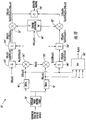
- a cellular communications system 20 in accordance with the present invention illustratively includes one or more cellular base stations 21 and a plurality of mobile cellular communications devices 22a-22n for communicating therewith. More particularly, the cellular base station 21 and the mobile cellular communications devices 22 each includes respective transmission and reception circuitry, which allows the mobile cellular communications devices to send and receive cellular communications signals to and from the cellular base station, and vice-versa.
- the mobile wireless communications devices 22 may be cellular telephones or multi-function devices which provide personal digital assistant (PDA) features (e.g., calendar, contacts, etc.) as well as electronic mail (email), Internet, image, and other features in addition to cellular voice functionality, as will be appreciated by those skilled in the art.
- PDA personal digital assistant
- email electronic mail
- Internet image, and other features in addition to cellular voice functionality, as will be appreciated by those skilled in the art.
- cellular telephone channels tend to be subject to Rayleigh fading.
- Rayleigh fading causes very rapid fluctuations in signal amplitude and phase.
- coherent modulation techniques are typically avoided in environments where this type of fading is prevalent, and differential modulation is instead used.
- FEC forward error correction
- the present invention extends the benefits of the above-noted modulation approach of Cobb et al. to cellular communications systems.
- the present invention is particularly well suited for GSM/GPRS/EDGE applications. That is, the present invention may be used to enhance the performance of existing GSM systems so that GPRS and/or EDGE services may be more readily implemented without significant network changes.
- the present invention will be described herein with reference to such an implementation, although it may be used with other cellular standards or systems as well.
- the present invention may allow cellular service providers to more readily implement GPRS and/or EDGE services.
- service providers may advantageously be able defer 3G rollouts, which will likely require significant replacements of base station infrastructure as well as obtaining new communications licenses, both of which may be extremely costly.
- the base station 21 and the mobile cellular communications devices 22 each includes respective transmission and reception circuitry which allow the base station to communicate with the mobile cellular communications devices, and vice-versa.
- the transmission circuitry is shown in the mobile cellular communications device 22a, and the reception circuitry is shown in the base station 21, to illustrate a transmission from the former to the latter.
- the respective transmission and reception circuitry of each of the mobile cellular communications devices 22 and the base station 21 are not show.
- the transmission circuitry illustratively includes an encoder 23 for generating an information signal from information such as voice and/or data (e.g., text, image, etc.) signals, for example.
- the encoder 23 may perform FEC encoding followed by interleaving operation to produce the information signal. While typical GSM systems may not provide for enhanced FEC schemes such as turbo codes, they may be used in accordance with the present invention for EDGE implementations, for example, as will be discussed further below.
- a standard transmission burst will include two guard band portions (GB) each including three guard band symbols 31 at the beginning and end of the burst ( FIG. 4 ). Furthermore, a training symbol section is included in the middle of the burst which has twenty-six training symbols 32, and the training symbol portion is immediately preceded and followed by a signaling symbol 33. Furthermore, a standard GSM burst also includes two information or data symbol portions, each of which includes fifty-seven data symbols 34. One of the data symbol portions precedes the training symbol portion, while the other follows it, as shown. It should be noted that in FIG. 4-6 spaces are shown between the guard band portions, data symbol portions, and training/signaling symbol portion for clarity of illustration only. In an actual transmission there would typically not be a transmission delay between the different symbol portions.
- the transmission circuitry also illustratively includes a modulator 25 for generating a modulated waveform based upon the information signal from the encoder 23, a carrier signal, and one or more phase reference symbols, as will be discussed further below.
- the modulator 25 illustratively includes an offset circuit 24 so that the modulated waveform includes a carrier frequency indicator, as will also be described further below.
- the modulator 25 is a Gaussian-filtered minimum shift keying (GMSK) modulator.
- GMSK Gaussian-filtered minimum shift keying
- the GPSK modulator 25 illustratively includes a Gaussian phase shaping filter 29 downstream from the offset circuit 24, which integrates the output of the offset circuit and applies Gaussian frequency pulse shaping thereto.
- Cosine (COS) and sine (SIN) function blocks 90, 91 are downstream from the Gaussian phase shaping filter 29 and generate in-phase (I) and quadrature (Q) components d I and d Q of the filtered information signal, respectively.
- the I and Q outputs from the cosine and sine function blocks 90, 91 are respectively combined with a carrier signal by mixers 26, 27, the outputs of which are summed by a summer 28 and provided to a transmitter 40 which cooperates with an associated antenna 41 to send the modulated waveform to the receive circuitry.
- the offset circuit 24 biases the information signal by creating an imbalance in the ratio of logic ones to zeros in the information sequence.
- This imbalance causes a predetermined amount of carrier energy to be "injected” into the spectral waveform, which appears as a spike at the desired carrier frequency.
- the carrier frequency indicator is a predetermined amount of unmodulated carrier energy (i.e., carrier "leakage") that is intentionally injected into the modulated waveform by the offset circuit 24.
- the injected frequency resulting from the imbalance facilitates detection and recovery of the carrier at the receiver without the need for a non-linear based carrier regeneration circuit in the carrier recovery path of the receiver, as is typical of prior art devices.
- the receive circuitry can detect and recover the carrier at a lower level of signal-to-noise ratio.
- the information signal generated by the FEC encoder 23 is a binary digital information signal.
- the offset circuit 24 changes values of the information signal (i.e., from logic 1 to logic 0, or vice-versa) to create the imbalance. That is, the offset circuit 24 determines if the information sequence has more logic ones than zeros, or vice-versa, or if it is substantially balanced in ones and zeros. If it is substantially balanced, the offset circuit 24 overwrites zeros with ones (or vice-versa) so that the ratio of ones to zeros is no longer one-to-one.
- the amount by which the ratio of ones to zeroes is to be changed will vary based upon the given application. For example, overwriting the ones and zeros introduces error in the information signal. The amount of error that can be tolerated will depend upon the type of error correction being used. Moreover, changing the ratio too much may result in an unacceptable amount of signal loss, as well as a violation of the applicable cellular standard.
- the imbalance be as small as possible to provide suitable detection on the receiving end.
- the ratio of logic ones to zeros may only need to be a few bits unbalanced (or less) to provide a suitably detectable carrier reference indicator.
- the ratio of logic ones and zeros in the information signal is carefully balanced (i.e., a one-to-one ratio) so that the carrier is suppressed.
- the offset circuit 24 may also format the modulated waveform into a plurality of symbols suitable for the particular type of transmission being used in a given implementation, as will be appreciated by those skilled in the art.
- the offset circuit 24 may insert a training symbol portion or sequence in accordance with an established cellular standard (e.g., GSM).
- GSM Global System for Mobile communications
- the offset circuit 24 also preferably inserts one or more phase reference symbols 35 (shown in solid black in FIGS. 4-6 for ease of reference) in the modulated waveform based upon the phase of the carrier signal. That is, the phase reference symbols indicate to the reception circuitry the original phase of the carrier signal so that discrepancies in phase which occur because of fading during transmission can be corrected, as will be discussed further below.
- phase symbols 35 are included in the training symbol portion of the waveform. Since the training symbols are predefined, the receive circuitry will have a priori knowledge of the phase corresponding to the received phase reference symbols 35. However, in other embodiments the phase reference symbols 35 may be located elsewhere. For example, phase reference symbols 35' may be located in the guard band portions ( FIG. 5 ). Further, phase reference symbols 35" may be located in the data symbol portions, as shown in FIG. 6 .
- phase reference symbols 35 may be located in more than one of the above noted symbol portions.
- phase reference symbols 35 are preferably in a form that is compliant with the particular cellular standard being used, and thus can be read by a typical cellular receiver designed for that standard, as will be appreciated by those skilled in the art. Additionally, a plurality of phase reference symbols 35 may be positioned in succession one after the next, and various spacings (including asymmetrical spacing) of the phase reference symbols may also be used, as will also be appreciated by those skilled in the art.
- the offset circuit 24 may overwrite logic ones or zeros to provide the carrier frequency indicator in the same manner just described for the phase reference symbols. That is, in one embodiment, .the offset circuit 24 overwrites one or more bits at randomly selected or predetermined locations in the data symbol portions, but not in the training symbol portion, to create the desired ratio of ones to zeros. In another embodiment, the offset circuit 24 overwrites one or more bits in the training symbol portion. In a still further embodiment, the offset circuit 24 instead of overwriting data or training bits may overwrite the symbols in the guard band portion(s) to unbalance the number of ones and zeros. Of course, symbols may be overwritten in more than one of the various GSM waveform portions.
- the offset circuit 24' includes a summer 95' for adding phase reference symbols 35 to the information signal, as discussed above. Yet, rather than using the cosine and sine function blocks 90, 91 to generate the I and Q components d I and d Q , this may instead be done by a demultiplexer (DEMUX) 96' in the offset circuit 24'.
- DEMUX demultiplexer
- the offset circuit 24' instead includes a DC offset circuit 97' for biasing one (or both) of the components d I , d Q so that the absolute value of the amplitude excursion that represents a data "one" is different from the absolute value of the amplitude excursion that represents a data "zero".
- the d I component is biased by a constant DC value k. This approach will similarly introduce unmodulated carrier energy (i.e., leakage) into the modulated waveform to provide a carrier frequency indicator, as will be appreciated by those skilled in the art.
- DC offset k may take various forms, i.e., this could be done using a chopped DC offset, etc. Further details on implementing the imbalance to cause carrier injection through carrier leakage and the advantages thereof may be found in the above-noted patent to Cobb et al.
- Another related approach to providing the carrier frequency indicator is to separate the information signal into I and Q components using the cosine and sine function blocks 90, 91, as illustrated in FIG. 2 , but to position the DC offset circuit 97' between the cosine processor 90 and mixer 26 (and/or between the sine processor 91 and the mixer 27 ).
- the end result from either case will be the injection of unmodulated carrier energy into the modulated waveform to provide the carrier frequency indicator, as with the other approaches described above.
- other suitable offset circuit 24 arrangements in addition to those described herein may also be used to provide the carrier frequency indicator.
- the base station 21 also includes one or more antennas 42 (illustratively shown as an antenna tower) and a front end 43 for receiving the modulated waveform. More particularly, the front end 23 illustratively includes ( FIG. 3 ) a matched filter 44 for filtering the received waveform, although other suitable filters may also be used, as will be appreciated by those skilled in the art.
- the front end 43 also illustratively includes an initial acquisition block 45 downstream from the RRC filter 44 for acquiring the received signal and communicating the acquisition to the remaining components.
- a bit/frame timing block 46 also downstream from the RRC filter is for generating a system timing signal based upon the received signal.
- a phase de-rotator 47 receives the system timing signal from the bit/frame timing block 46, and an output of the phase de-rotator is provided as an input to a mixer 48 along with the output of the RRC filter 44. The output of the mixer 48 is de-multiplexed by a de-multiplexer 49 based upon the system timing signal.
- the outputs of the de-multiplexer 49 are respectively connected to a carrier reconstructor 50 and a demodulator 51.
- the carrier reconstructor 50 derives a local estimate of the carrier without recourse to a non-linear operation such as raising the signal (plus noise) to a power, which would normally be necessary in prior art receivers.
- the carrier reconstructor 50 exploits the carrier frequency indicator and phase reference symbols injected by the transmission circuitry to reconstruct the carrier using linear operations. This has the advantage of avoiding the noise enhancement affect of non-linear operations and allows the receiver to reconstruct the carrier at lower signal-to-noise ratios than would be possible if a non-linear operation was required. See the above-noted Cobb et al. patent for further details on this effect.
- the carrier reconstructor 50 illustratively includes a phase symbol correlator 52 connected to a first output of the de-multiplexer 49, and a phase/frequency estimator 53 downstream from the phase symbol correlator.
- ⁇ tan ⁇ 1 Im r Re r
- the phase/frequency estimator 53 determines (i.e., estimates) the original phase and frequency of the carrier signal, as will be appreciated by those skilled in the art.
- the phase/frequency estimator 53 may include a phase-lock loop, as discussed further in the Cobb et al. patent noted above.
- phase reference symbols 35 may be used to estimate the phase based upon the phase reference symbols 35.
- One approach is to use a mean estimation, i.e., to measure the average phase of phase reference symbols 35 present in a given GSM burst. Generally speaking, this may be done by summing the real and imaginary parts, respectively, of the correlated phase reference symbols 35 and inverting the sign of the imaginary sum, as will be appreciated by those skilled in the art.
- phase is represented by a line where the first and last reference symbols define the endpoints of the line. More particularly, using this approach the first and last phase reference symbols in each frame are sampled, and the real and imaginary parts of each phase reference symbol are summed and a phase of the resulting sums is determined. The change in phase across the frame is calculated and converted to a change in phase per symbol. Based upon the initial phase and the phase change per symbol, the phase of each symbol is calculated. The negative of the respective phase for each symbol and its real portion provide the carrier reference for demodulating that symbol, as will be appreciated by those skilled in the art.
- the phase may be represented by a line whose slope fits a minimum mean square error of the phase reference symbol. To do so, all of the phase reference symbols 35 in a burst are sampled and the phase of each is determined. Using a minimum mean squared algorithm, the offset and slope of the best fitting straight line through these points is derived. Using the equation of this line, a phase estimate is calculated for each symbol. Again, the negative of this phase and its real counterpart for each symbol provide the carrier reference for decoding that symbol.
- phase estimation approaches may also be used, as will be appreciated by those skilled in the art.
- the particular approach to be used will depend upon factors such as the number and placement of the phase reference symbols 35 in the burst, the amount of bit error rate (BER) than can be tolerated, phase accuracy required, etc., for a given implementation, as will be appreciated by those skilled in the art.
- BER bit error rate
- the demodulator 51 demodulates the I and Q components of the information signal based upon the phase and frequency of the carrier signal determined by the phase/frequency estimator 53 to create "soft decision" estimates of the bits in the data portions of the received waveform.
- a soft decision includes a preliminary estimate of a data bit coupled with a measure of the confidence of that bit decision.
- the demodulator 51 may include an equalizer (not shown) to compensate for the effects of the radio channel, as will also be appreciated by those skilled in the art.
- GMSK modulator in this embodiment is determined by the waveform standard for the cellular system, GPS and GPRS in this case, in which the receiver is intended to operate and that demodulator 51 may take other forms for other modulation formats (e.g., QPSK, 8PSK, QAM) as provided in the applicable cellular system standard.
- demodulator 51 may take other forms for other modulation formats (e.g., QPSK, 8PSK, QAM) as provided in the applicable cellular system standard.
- a decoder 54 (e.g., an FEC decoder) is downstream from the demodulator 51 and reproduces the information based upon the demodulated I and Q components d I , d Q , as will be appreciated by those skilled in the art.
- the decoder 54 may perform a de-interleaving operation in series with error correction decoding, as will also be appreciated by those skilled in the art.
- components may be implemented in various forms.
- components may be implemented as electronic circuits, while in others they may be implemented using processors (e.g., a digital signal processor (DSP)) and software, as will be appreciated by those skilled in the art.
- DSP digital signal processor
- an information signal is generated, at Block 71, and a modulated waveform is generated based upon the information signal, a carrier signal, and at least one phase reference symbol so that it includes a carrier frequency indicator, at Block 72, as discussed previously above.
- the method further includes transmitting the modulated waveform to the cellular base station 21, at Block 73 , thus concluding the illustrated method (Block 74 ).
- a mobile cellular communications device 22 or the base station 21 receives a modulated waveform, at Block 81, determines the phase of the carrier signal based upon the phase reference symbol(s) 35 therein, and determines the frequency of the carrier signal based upon the carrier frequency indicator (Block 82 ), as discussed above.
- the information signal is demodulated (Block 83 ) based upon the determined phase and frequency of the carrier signal, thus concluding the illustrated method (Block 84 ).
- the present invention provides numerous advantages.
- the lock range of the demodulator 51 may be extended to provide improved link acquisition at very low signal-to-noise ratios.
- the present invention allows the cellular system 20 to exploit the benefit of error correction at these low signal-to-noise ratios.
- the present invention allows services such as EDGE to more fully realize the benefits of the improved coding gain associated with more powerful error correction codes, such as turbo codes.
- it allows the waveform to conform with the established cellular standards so that legacy base stations and mobile devices that do not incorporate the present invention may interoperate with base stations and mobile devices that do incorporate it, albeit without obtaining the benefits of the present invention.
- This example is directed to an MSK modulation arrangement.
- This design is particularly applicable to a GSM/GPRS system, which uses GMSK modulation, and may also be useful in EDGE systems that use GMSK and 8PSK.
- the modulator described in this example has the added benefit of maintaining the constant envelope property of the signal, which provides opportunities for improved power efficiencies. This is particularly important in battery operated mobile communications devices such as those used in cellular communications systems.
- a predetermined amount of unmodulated carrier energy is added to the standard modulated waveform to provide the carrier frequency indicator. More particularly, a small amount of carrier leakage (hereafter “carrier injection”) is created by manipulation of the baseband signal.
- carrier injection a small amount of carrier leakage
- This provides opportunities for design efficiencies and for tailoring the signal to maintain desirable characteristics such as a constant envelope or low out-of-band emissions. However, as noted above, this could also be accomplished during the modulation process, if desired.
- x t Acos ⁇ t + ⁇ t
- A is a constant
- ⁇ (t) is the phase modulation that carries the information.
- compensation functions f 1 ( ⁇ (t)) and f 2 ( ⁇ (t)) are selected to insure constant envelope, and offset constant c provides the carrier injection. It will be appreciated by those skilled in the art that there are many possibly choices for these functions and constants.
- FIG. 10 An embodiment of the modulator 25" for implementing the foregoing is shown in FIG. 10 .
- the information signal with phase reference symbols is input to the Gaussian phase shaping filter 29", which is followed by the cosine and sine function blocks 90", 91".
- the output of the cosine function block 90" (cos( ⁇ (t))) is connected to a function generator 100" and a mixer (i.e., multiplier) 101".
- the output of the sine function block 91" sin( ⁇ (t))
- the function generator 100" also receives as inputs the constant K and carrier injection value c , and it outputs f( ⁇ (t)) in accordance with equation (8), above.
- the output of the function generator 100" is connected to both of the mixers 101", 102", which respectively provide outputs f( ⁇ (t))cos( ⁇ (t)) and f( ⁇ (t))sin( ⁇ (t)).
- the output of the mixer 101" is connected to a subtractor 103", which also receives sin( ⁇ (t)) as a second input and thus provides as its output sin( ⁇ (t))-f( ⁇ (t))cos( ⁇ (t)).
- the output of the mixer 102" is connected to a summer 104", which also receives cos( ⁇ (t)) as an input and thus provides as its output cos( ⁇ (t))+f( ⁇ (t))sin( ⁇ (t)).
- the carrier injection value c is added to the outputs of the subtractor 103" and summer 104" via summers 105" and 106" to provide the values sin( ⁇ (t))-f( ⁇ (t))cos( ⁇ (t))+c and cos( ⁇ (t))+f( ⁇ (t))sin( ⁇ (t))+c, respectively.
- a carrier generator 107 which receives as its input cos( ⁇ t), via the mixers 26", 27” to provide the values cos( ⁇ (t))+f( ⁇ (t))sin( ⁇ (t))+c]cos( ⁇ t) and [sin( ⁇ )(t))-f( ⁇ (t))cos( ⁇ (t))+c]sin( ⁇ t).
- a subtractor 108 which provides the value s(t) as set forth in equation (6) above as the modulated waveform.
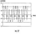
- FIG. 11 shows a typical prior art QPSK waveform similar to that represented by equations (1) and (3).
- QPSK was selected for this illustrative example for clarity of explanation because it is a constant envelope modulation that uses a relatively simple phase modulation function ⁇ (t).
- Desired demodulation of the modulated waveform may be accomplished using the receiver structure shown in FIG. 3 , where the demodulator 51 is implemented as a conventional correlation demodulator, in which the local correlation reference signals have the form defined in equations (6) and (8).
- the carrier recovery circuitry in such a demodulator would take advantage of the carrier component in the waveform and the phase reference symbols to enable it to operate at very low signal-to-noise ratios.
- the additional terms in equation (6) will appear as small distortion terms to a demodulator, which is designed for the waveform of equation (1), which will be the case for prior art cellular receivers that do not include this invention.
- the combined addition of the compensation functions and the offset constant in the modulated signal provides superior performance when the receiver is designed to exploit them, while a standard, prior art demodulator that is not designed to exploit these features may still demodulate the data.
Description
- Cellular communications systems continue to grow in popularity and have become an integral part of both personal and business communications. Cellular phones allow users to place and receive voice calls most anywhere they travel. Moreover, as cellular telephone technology has increased, so too has the functionality of cellular devices. For example, many cellular devices now incorporate personal digital assistant (PDA) features such as calendars, address books, task lists, etc. Moreover, such multi-function devices may also allow users to wirelessly access electronic mail (email) messages and the Internet via a cellular network.
- Various cellular communications standards have been developed for cellular communications systems. One of the more prominent standards is the Global System for Mobile Communications (GSM) for digital cellular systems. To more readily accommodate new services such as email, Internet, video, etc., GSM cellular systems are gradually moving toward third generation (3G) technology. General Packet Radio Service (GPRS) is one important advancement in the migration to 3G. GPRS allows a permanent data connection and free information flow for the end user's mobile cellular communications device. GPRS also provides for a more advanced billing and charging system. That is, it allows charging based on the services that a user will access, not simply the duration of the connection.
- Another advancement in the migration to 3G is the Enhanced Data Rates for Global Evolution (EDGE). EDGE will allow data speeds up to 384 kbit/s so that the advantages of GPRS may be fully utilized with fast connection set-up and higher bandwidth than traditional GSM technology.
- One potential difficulty in the evolution to GPRS and EDGE is that some GSM systems may not be set up to provide the low bit error rate (BER) performance necessary for these services. Achieving high data rates at a low BER may in some cases require large scale additions of base stations, which would result in a substantial cost to a cellular service provider.
- In addition, cellular communications often occur in environments where severe fading (i.e., Rayleigh fading) is encountered, which tends to cause burst bit errors. Many of the current GSM/GPRS implementations are designed for voice services, which may be more forgiving with respect to fading and burst bit errors than other services. That is, data services generally require improved error performance, which may result in lower data rates and/or increased numbers of retransmissions. As a result, throughput is decreased, which results in higher costs for the cellular service provider.
- One approach for addressing the effects of Rayleigh fading is generally discussed in an article entitled "An analysis of Pilot Symbol Assisted Modulation for Rayleigh Fading Channels" by Carvers, IEEE Transaction on Vehicular Technology, vol. 40, no. 4, Nov. 1991. Carvers discusses the use of pilot symbol assisted modulation (PSAM) to mitigate the effects of rapid fading in mobile communications applications. For PSAM, the transmitter periodically inserts known symbols, from which the receiver derives its amplitude and phase reference. While PSAM reduces the effective bit rate and introduces delay (requiring additional buffer space) at the receiver, Carvers notes that it also advantageously suppresses the error floor and enables multilevel modulation without changing the transmitted pulse shape or peak-to-average power ratio.
- Document
US 66 06 357 B1 discloses a satellite communications system using QPSK modulation scheme that uses a data spreading mechanism to rob a relatively limited portion of available transmitter power, and inject into the QPSK waveform a prescribed amount of carrier signal power, through which detection and non-regenerative extraction of the carrier at the receiver may be achieved without incurring a signal-to-noise degradation penalty. An in-phase (I) channel and quadrature-phase (Q) channel data symbols di and dq, disclosed therein, are encoded in an encoder with a prescribed forward error correction code, and coupled to associated mixers to which a carrier signal fc is also applied. The encoded data symbol streams are defined as excursions between prescribed voltage levels. In addition, the data signal path of one of the channels is summed with a prescribed D.C. voltage level, so as to provide an offset from the ideal normalized value. The insertion of this DC onset voltage shifts or biases the reference levels for the encoded in-phase data symbol stream to values of 1.k volts and (-1.0+0.k volts). The resultant phase quadrature modulated signals produced by mixers are then summed in a summing unit to produce a composite QPSK signal, that is transmitted via amplifier-feed circuitry coupled to an antenna. The signals received by an antenna are coupled to a single demodulator loop. To demodulate the data, the received signal is coupled to a carrier recovery path and a data recovery path. - Document
US 6 430 212 B1 discloses a communication device including a transmitter and receiver. The transmitter includes an M-ary encoder configured to generate an M-1 number of distinctive symbols each comprising k bits. M is equal to 2 and k is a positive integer. The transmitter also includes a code generator configured to produce spread spectrum codeword sequences based on the symbols generated by the M-ary encoder and based on a first and a second Gold code polynomials. The transmitter sends a radio signal based on the spread spectrum codeword sequences. The receiver is configured to receive the radio signal. The receiver includes a first shift register configured to receive an input signal generated based on the received radio signal and a second shift register configured to receive and circularly shift a locally generated codeword sequence that is identical to the codeword sequence used to encode the symbols. The receiver also includes an accumulator coupled to the first and second shift registers and configured to multiply and accumulate stored values in the first and second shift registers each time the second shift register is circularly shifted and a selecting device coupled to the accumulator and configured to identify one symbol from the plurality of symbols based on outputs from the accumulator. -
Document EP 0 113 246 A2 discloses a radio communication system comprised of a transmitter unit, a transmission line, and a receiver unit. The transmitter unit modulates an in-phase-channel (I-ch) data signal and quadrature-channel (Q-ch) data signal with two carriers having n/2 phase difference with each other. A DC offset is added to either one of the I-ch and Q-ch data signals before the modulation. In the receiver unit, a demodulation operation is performed for the received transmission signal through a synchronous detection with the use of a leakage carrier created due to the DC offset and included in the transmission signal. - Despite such prior art approaches, further improvements may be desirable when implementing new services and functionality with existing GSM or other cellular systems.
- In view of the foregoing background, it is therefore an object of the present invention to provide improved error performance signal characteristic tracking in cellular communications systems and related methods according to the independent claims. Another object of the present invention is to maintain compatibility and interoperability with existing cellular standard base stations and mobile communications equipment.
- These and other objects, features, and advantages in accordance with the present invention are provided by a cellular communications system which may include at least one cellular base station and a plurality of mobile cellular communications devices for communicating therewith. More particularly, the at least one cellular base station and the mobile cellular communications devices may each include an encoder for generating an information signal. A modulator may also be included for generating a modulated waveform based upon the information signal, a carrier signal having a frequency and phase associated therewith, and at least one carrier phase reference symbol. The modulator may include an offset circuit so that the modulated waveform includes a carrier frequency indicator. In addition, a transmitter may also be included for transmitting the modulated waveform.
- By way of example, the offset circuit may bias the information signal, and the carrier frequency indicator may be based upon the bias of the information signal. The carrier frequency indicator may be a predetermined amount of unmodulated carrier energy (i.e., carrier "leakage"). More specifically, the information signal may be a binary digital information signal, and the offset circuit may bias the binary digital information signal by changing values thereof (i.e., from
logic 1 tologic 0, or vice-versa). That is, the offset circuit preferably creates an imbalance between ones and zeros in the binary information sequence for biasing the information signal to create carrier leakage in the transmitted signal, which provides the carrier frequency indicator for a receiver. - Moreover, the offset circuit may change the values of the binary digital information signal based upon a ratio of first to second logic values in the binary digital information signal. For example, the offset circuit may determine if the information sequence has more logic ones than zeros, or vice-versa, or if it is substantially balanced in ones and zeros. If it is substantially balanced, the offset circuit overwrites zeros with ones (or vice-versa) so that the ratio of ones to zeros is no longer one-to-one.
- By contrast, in common prior art modulators for cellular systems, the ratio of
logic 1's and 0's in the information is carefully balanced (i.e., a one-to-one ratio) so that the carrier is suppressed. In such prior art modulators, carrier leakage is considered detrimental to the system operation. However, in accordance with the present invention, carrier leakage is deliberately induced by the "imbalance" in logic values imposed by the offset circuit to inject a small amount of unmodulated carrier energy into the modulated waveform as the carrier frequency indicator, yet without violating the applicable cellular standard. This advantageously allows a receiver to more readily recover the carrier frequency at a lower signal to noise ratio or by using less complicated circuitry, for example. - The offset circuit may also separate the information signal into in-phase (I) and quadrature (Q) components. As such, an alternate approach for the offset circuit to bias the information signal is to bias one or both of the I and Q components with a direct current (DC) offset.
- Each of the mobile cellular communications devices and the at least one base station may further include a front end for receiving a modulated waveform, and a carrier reconstructor for determining the phase of the carrier signal associated with the received modulated waveform based upon the at least one phase reference symbol, and for determining the frequency of the carrier signal based upon the carrier frequency indicator. A demodulator may also be included for demodulating the information signal based upon the determined phase and frequency of the carrier signal, as well as a decoder for decoding the demodulated information signal.
- Furthermore, the at least one phase reference symbol may be a plurality thereof. As such, the carrier reconstructor may include a phase symbol correlator for correlating the plurality of phase reference symbols. By way of example, the modulated waveform may include a training symbol portion, and the offset circuit may insert the at least one phase reference symbol in the training symbol portion. Similarly, the modulated waveform may include one or more guard band portions and/or data symbol portions, and the offset circuit may insert the at least one phase reference symbol in the guard band and/or data symbol portions. The offset circuit may similarly change the values of the binary digital information signal in the training symbol portion, the guard band portion(s), and/or the data symbol portion(s) to provide the carrier frequency indicator, as noted above.
- The modulator may be a Gaussian-filtered minimum shift keying (GMSK) modulator, for example. Also, the at least one cellular base station and the mobile cellular communications devices may operate in accordance with one or more of the Global System for Mobile Communications (GSM) standard, the General Packet Radio Service (GPRS) standard, and the Enhanced Data Rates for Global Evolution (EDGE) standard. Further, the encoder may be a forward error correction (FEC) encoder, for example.
- A method aspect of the invention is for communicating between a mobile cellular communications device and a cellular base station. The method may include generating an information signal, and generating a modulated waveform based upon the information signal, a carrier signal having a frequency and phase associated therewith, and at least one carrier phase reference symbol. The modulated waveform may be generated using a modulator including an offset circuit so that the modulated waveform includes a carrier frequency indicator. The method may further include transmitting the modulated waveform.
- Yet another method aspect of the invention is for communicating between a mobile cellular communications device and a cellular base station. The method may include receiving a modulated waveform generated based upon an information signal, a carrier signal having a frequency and phase associated therewith, and at least one carrier phase reference symbol, where the modulated waveform has a carrier frequency indicator associated therewith. The method may further include determining the phase of the carrier signal based upon the at least one phase reference symbol, determining the frequency of the carrier signal based upon the carrier frequency indicator, and demodulating the information signal based upon the determined phase and frequency of the carrier signal.
-
-
FIG. 1 is a schematic block diagram of a cellular communications system in accordance with the present invention. -
FIG. 2 is schematic block diagram further illustrating the transmission circuitry of the cellular communications system ofFIG. 1 . -
FIG. 3 is schematic block diagram further illustrating the reception circuitry of the cellular communications system ofFIG. 1 . -
FIGS. 4-6 are waveform diagrams illustrating symbols of a waveform for a GSM implementation of the cellular communications system ofFIG. 1 including phase reference symbols. -
FIGS. 7-8 are flow diagrams illustrating cellular communications methods in accordance with the present invention. -
FIG. 9 is a schematic block diagram illustrating an alternate embodiment of the offset circuit ofFIG. 1 . -
FIG. 10 is a schematic block diagram of an alternate embodiment of the modulator ofFIG. 2 . -
FIG. 11 is a graph illustrating a QPSK waveform in accordance with the prior art. -
FIG. 12 is a graph illustrating a QPSK waveform offset to provide a carrier frequency indicator in accordance with the present invention. -
FIG. 13 is a graph illustrating a constant envelope waveform in accordance with the present invention. - The present invention will now be described more fully hereinafter with reference to the accompanying drawings, in which preferred embodiments of the invention are shown. This invention may, however, be embodied in many different forms and should not be construed as limited to the embodiments set forth herein. Rather, these embodiments are provided so that this disclosure will be thorough and complete, and will fully convey the scope of the invention to those skilled in the art. Like numbers refer to like elements throughout, and prime and multiple notation are used to indicate similar elements in alternate embodiments.
- Referring initially to
FIGS. 1-6 , acellular communications system 20 in accordance with the present invention illustratively includes one or morecellular base stations 21 and a plurality of mobilecellular communications devices 22a-22n for communicating therewith. More particularly, thecellular base station 21 and the mobile cellular communications devices 22 each includes respective transmission and reception circuitry, which allows the mobile cellular communications devices to send and receive cellular communications signals to and from the cellular base station, and vice-versa. By way of example, the mobile wireless communications devices 22 may be cellular telephones or multi-function devices which provide personal digital assistant (PDA) features (e.g., calendar, contacts, etc.) as well as electronic mail (email), Internet, image, and other features in addition to cellular voice functionality, as will be appreciated by those skilled in the art. - As noted above, cellular telephone channels tend to be subject to Rayleigh fading. Rayleigh fading causes very rapid fluctuations in signal amplitude and phase. As a result, coherent modulation techniques are typically avoided in environments where this type of fading is prevalent, and differential modulation is instead used. However, the inability to use coherent demodulation techniques reduces the performance that can be achieved, even when fairly powerful forward error correction (FEC) techniques, such as turbo codes, are used in the communications link.
- In cellular applications, fading typically results from multi-path transmissions and blockage, as will be appreciated by those skilled in the art. Of course, fading is not unique to cellular communications, and it can be problematic in other applications such as satellite-based communications as well. One particularly advantageous approach for addressing problems caused by fading in satellite communications is disclosed in
U.S. Patent No. 6,606,357 to Cobb et al. , which is assigned to the Assignee of the present application, and which is hereby incorporated herein in its entirety by reference. Generally speaking, Cobb et al. discloses a carrier injection waveform-based modulation approach that may be used to facilitate detection and recovery of the carrier at the receiver. - The present invention extends the benefits of the above-noted modulation approach of Cobb et al. to cellular communications systems. In particular, the present invention is particularly well suited for GSM/GPRS/EDGE applications. That is, the present invention may be used to enhance the performance of existing GSM systems so that GPRS and/or EDGE services may be more readily implemented without significant network changes. Thus, for convenience of explanation, the present invention will be described herein with reference to such an implementation, although it may be used with other cellular standards or systems as well.
- As will be further understood from the following description, the present invention may allow cellular service providers to more readily implement GPRS and/or EDGE services. Thus, service providers may advantageously be able defer 3G rollouts, which will likely require significant replacements of base station infrastructure as well as obtaining new communications licenses, both of which may be extremely costly.
- The
base station 21 and the mobile cellular communications devices 22 each includes respective transmission and reception circuitry which allow the base station to communicate with the mobile cellular communications devices, and vice-versa. The transmission circuitry is shown in the mobilecellular communications device 22a, and the reception circuitry is shown in thebase station 21, to illustrate a transmission from the former to the latter. However, for clarity of illustration, the respective transmission and reception circuitry of each of the mobile cellular communications devices 22 and thebase station 21 are not show. - More particularly, the transmission circuitry illustratively includes an
encoder 23 for generating an information signal from information such as voice and/or data (e.g., text, image, etc.) signals, for example. By way of example, theencoder 23 may perform FEC encoding followed by interleaving operation to produce the information signal. While typical GSM systems may not provide for enhanced FEC schemes such as turbo codes, they may be used in accordance with the present invention for EDGE implementations, for example, as will be discussed further below. - In the case of a GSM implementation, a standard transmission burst will include two guard band portions (GB) each including three
guard band symbols 31 at the beginning and end of the burst (FIG. 4 ). Furthermore, a training symbol section is included in the middle of the burst which has twenty-sixtraining symbols 32, and the training symbol portion is immediately preceded and followed by asignaling symbol 33. Furthermore, a standard GSM burst also includes two information or data symbol portions, each of which includes fifty-sevendata symbols 34. One of the data symbol portions precedes the training symbol portion, while the other follows it, as shown. It should be noted that inFIG. 4-6 spaces are shown between the guard band portions, data symbol portions, and training/signaling symbol portion for clarity of illustration only. In an actual transmission there would typically not be a transmission delay between the different symbol portions. - The transmission circuitry also illustratively includes a
modulator 25 for generating a modulated waveform based upon the information signal from theencoder 23, a carrier signal, and one or more phase reference symbols, as will be discussed further below. In accordance with the invention, themodulator 25 illustratively includes an offsetcircuit 24 so that the modulated waveform includes a carrier frequency indicator, as will also be described further below. - In the exemplary embodiment illustrated in
FIG. 2 for a GSM implementation, themodulator 25 is a Gaussian-filtered minimum shift keying (GMSK) modulator. However, it will be appreciated by those skilled in the art that other modulators may be used in accordance with the present invention for other cellular standards, such as an 8PSK modulator in the case of EDGE, for example. TheGPSK modulator 25 illustratively includes a Gaussianphase shaping filter 29 downstream from the offsetcircuit 24, which integrates the output of the offset circuit and applies Gaussian frequency pulse shaping thereto. - Cosine (COS) and sine (SIN) function blocks 90, 91 are downstream from the Gaussian
phase shaping filter 29 and generate in-phase (I) and quadrature (Q) components dI and dQ of the filtered information signal, respectively. The I and Q outputs from the cosine and sine function blocks 90, 91 are respectively combined with a carrier signal bymixers summer 28 and provided to atransmitter 40 which cooperates with an associatedantenna 41 to send the modulated waveform to the receive circuitry. - Generally speaking, the offset
circuit 24 biases the information signal by creating an imbalance in the ratio of logic ones to zeros in the information sequence. This imbalance causes a predetermined amount of carrier energy to be "injected" into the spectral waveform, which appears as a spike at the desired carrier frequency. Stated alternately, the carrier frequency indicator is a predetermined amount of unmodulated carrier energy (i.e., carrier "leakage") that is intentionally injected into the modulated waveform by the offsetcircuit 24. Thus, the injected frequency resulting from the imbalance facilitates detection and recovery of the carrier at the receiver without the need for a non-linear based carrier regeneration circuit in the carrier recovery path of the receiver, as is typical of prior art devices. As such, the receive circuitry can detect and recover the carrier at a lower level of signal-to-noise ratio. - As noted above, the information signal generated by the
FEC encoder 23 is a binary digital information signal. The offsetcircuit 24 changes values of the information signal (i.e., fromlogic 1 tologic 0, or vice-versa) to create the imbalance. That is, the offsetcircuit 24 determines if the information sequence has more logic ones than zeros, or vice-versa, or if it is substantially balanced in ones and zeros. If it is substantially balanced, the offsetcircuit 24 overwrites zeros with ones (or vice-versa) so that the ratio of ones to zeros is no longer one-to-one. - Generally speaking, the greater the imbalance in the ratio of logic ones to zeros, the greater the amount of unmodulated carrier energy that will be injected into the modulated waveform. Of course, the amount by which the ratio of ones to zeroes is to be changed will vary based upon the given application. For example, overwriting the ones and zeros introduces error in the information signal. The amount of error that can be tolerated will depend upon the type of error correction being used. Moreover, changing the ratio too much may result in an unacceptable amount of signal loss, as well as a violation of the applicable cellular standard.
- Accordingly, it is preferable that the imbalance be as small as possible to provide suitable detection on the receiving end. For a GSM waveform, the ratio of logic ones to zeros may only need to be a few bits unbalanced (or less) to provide a suitably detectable carrier reference indicator. By contrast, in common prior art modulators for cellular systems, the ratio of logic ones and zeros in the information signal is carefully balanced (i.e., a one-to-one ratio) so that the carrier is suppressed.
- The offset
circuit 24 may also format the modulated waveform into a plurality of symbols suitable for the particular type of transmission being used in a given implementation, as will be appreciated by those skilled in the art. For example, the offsetcircuit 24 may insert a training symbol portion or sequence in accordance with an established cellular standard (e.g., GSM). The result is an input sequence signal that includes the biased information signal along with any applicable reference symbols and/or training symbols formatted in accordance with the standard for a particular cellular system application. - In addition, the offset
circuit 24 also preferably inserts one or more phase reference symbols 35 (shown in solid black inFIGS. 4-6 for ease of reference) in the modulated waveform based upon the phase of the carrier signal. That is, the phase reference symbols indicate to the reception circuitry the original phase of the carrier signal so that discrepancies in phase which occur because of fading during transmission can be corrected, as will be discussed further below. - In the example illustrated in
FIG. 4 , thephase symbols 35 are included in the training symbol portion of the waveform. Since the training symbols are predefined, the receive circuitry will have a priori knowledge of the phase corresponding to the receivedphase reference symbols 35. However, in other embodiments thephase reference symbols 35 may be located elsewhere. For example, phase reference symbols 35' may be located in the guard band portions (FIG. 5 ). Further,phase reference symbols 35" may be located in the data symbol portions, as shown inFIG. 6 . - Distributing the phase reference symbols advantageously provides enhanced phase tracking. Again, while this introduces a deliberate error in the information transmitted within the waveform, it may also provide enhanced phase tracking, and a certain amount of error may be tolerable because of the FEC. In other embodiments,
phase reference symbols 35 may be located in more than one of the above noted symbol portions. - It should be noted that the
phase reference symbols 35 are preferably in a form that is compliant with the particular cellular standard being used, and thus can be read by a typical cellular receiver designed for that standard, as will be appreciated by those skilled in the art. Additionally, a plurality ofphase reference symbols 35 may be positioned in succession one after the next, and various spacings (including asymmetrical spacing) of the phase reference symbols may also be used, as will also be appreciated by those skilled in the art. - The offset
circuit 24 may overwrite logic ones or zeros to provide the carrier frequency indicator in the same manner just described for the phase reference symbols. That is, in one embodiment, .the offsetcircuit 24 overwrites one or more bits at randomly selected or predetermined locations in the data symbol portions, but not in the training symbol portion, to create the desired ratio of ones to zeros. In another embodiment, the offsetcircuit 24 overwrites one or more bits in the training symbol portion. In a still further embodiment, the offsetcircuit 24 instead of overwriting data or training bits may overwrite the symbols in the guard band portion(s) to unbalance the number of ones and zeros. Of course, symbols may be overwritten in more than one of the various GSM waveform portions. - Yet another embodiment for providing the carrier frequency indicator is now described with reference to
FIG. 9 . In this embodiment, the offset circuit 24' includes a summer 95' for addingphase reference symbols 35 to the information signal, as discussed above. Yet, rather than using the cosine and sine function blocks 90, 91 to generate the I and Q components dI and dQ , this may instead be done by a demultiplexer (DEMUX) 96' in the offset circuit 24'. - Further, rather than unbalancing the ratio of logic ones to zeros in the information sequence as discussed above, the offset circuit 24' instead includes a DC offset circuit 97' for biasing one (or both) of the components dI, dQ so that the absolute value of the amplitude excursion that represents a data "one" is different from the absolute value of the amplitude excursion that represents a data "zero". In the illustrated embodiment, the dI component is biased by a constant DC value k. This approach will similarly introduce unmodulated carrier energy (i.e., leakage) into the modulated waveform to provide a carrier frequency indicator, as will be appreciated by those skilled in the art. It should be noted that the DC offset k may take various forms, i.e., this could be done using a chopped DC offset, etc. Further details on implementing the imbalance to cause carrier injection through carrier leakage and the advantages thereof may be found in the above-noted patent to Cobb et al.
- Another related approach to providing the carrier frequency indicator is to separate the information signal into I and Q components using the cosine and sine function blocks 90, 91, as illustrated in
FIG. 2 , but to position the DC offset circuit 97' between thecosine processor 90 and mixer 26 (and/or between thesine processor 91 and the mixer 27). As will be appreciated by those skilled in the art, the end result from either case will be the injection of unmodulated carrier energy into the modulated waveform to provide the carrier frequency indicator, as with the other approaches described above. Of course, other suitable offsetcircuit 24 arrangements in addition to those described herein may also be used to provide the carrier frequency indicator. - Turning now to the receive circuitry, the
base station 21 also includes one or more antennas 42 (illustratively shown as an antenna tower) and afront end 43 for receiving the modulated waveform. More particularly, thefront end 23 illustratively includes (FIG. 3 ) a matchedfilter 44 for filtering the received waveform, although other suitable filters may also be used, as will be appreciated by those skilled in the art. - The
front end 43 also illustratively includes aninitial acquisition block 45 downstream from theRRC filter 44 for acquiring the received signal and communicating the acquisition to the remaining components. A bit/frame timing block 46 also downstream from the RRC filter is for generating a system timing signal based upon the received signal. Aphase de-rotator 47 receives the system timing signal from the bit/frame timing block 46, and an output of the phase de-rotator is provided as an input to amixer 48 along with the output of theRRC filter 44. The output of themixer 48 is de-multiplexed by a de-multiplexer 49 based upon the system timing signal. - The outputs of the de-multiplexer 49 are respectively connected to a
carrier reconstructor 50 and ademodulator 51. Thecarrier reconstructor 50 derives a local estimate of the carrier without recourse to a non-linear operation such as raising the signal (plus noise) to a power, which would normally be necessary in prior art receivers. In this case, thecarrier reconstructor 50 exploits the carrier frequency indicator and phase reference symbols injected by the transmission circuitry to reconstruct the carrier using linear operations. This has the advantage of avoiding the noise enhancement affect of non-linear operations and allows the receiver to reconstruct the carrier at lower signal-to-noise ratios than would be possible if a non-linear operation was required. See the above-noted Cobb et al. patent for further details on this effect. - More particularly, the
carrier reconstructor 50 illustratively includes aphase symbol correlator 52 connected to a first output of the de-multiplexer 49, and a phase/frequency estimator 53 downstream from the phase symbol correlator. Thephase symbol correlator 52 performs a complex multiplication of the receivedphase reference symbols 35 plus noise with local phase symbols. This multiplication produces a complex product, r(t), including noise, whose phase, ϕ, can be measured as
- From the output of the
phase symbol correlator 52 and the carrier frequency indicator (i.e., the predetermined amount of unmodulated carrier energy) present in the I and Q components of the received waveform, the phase/frequency estimator 53 determines (i.e., estimates) the original phase and frequency of the carrier signal, as will be appreciated by those skilled in the art. By way of example, the phase/frequency estimator 53 may include a phase-lock loop, as discussed further in the Cobb et al. patent noted above. - Various approaches may be used to estimate the phase based upon the
phase reference symbols 35. One approach is to use a mean estimation, i.e., to measure the average phase ofphase reference symbols 35 present in a given GSM burst. Generally speaking, this may be done by summing the real and imaginary parts, respectively, of the correlatedphase reference symbols 35 and inverting the sign of the imaginary sum, as will be appreciated by those skilled in the art. - Another approach is to use an end-to-end approach, in which the phase is represented by a line where the first and last reference symbols define the endpoints of the line. More particularly, using this approach the first and last phase reference symbols in each frame are sampled, and the real and imaginary parts of each phase reference symbol are summed and a phase of the resulting sums is determined. The change in phase across the frame is calculated and converted to a change in phase per symbol. Based upon the initial phase and the phase change per symbol, the phase of each symbol is calculated. The negative of the respective phase for each symbol and its real portion provide the carrier reference for demodulating that symbol, as will be appreciated by those skilled in the art.
- Similarly, the phase may be represented by a line whose slope fits a minimum mean square error of the phase reference symbol. To do so, all of the
phase reference symbols 35 in a burst are sampled and the phase of each is determined. Using a minimum mean squared algorithm, the offset and slope of the best fitting straight line through these points is derived. Using the equation of this line, a phase estimate is calculated for each symbol. Again, the negative of this phase and its real counterpart for each symbol provide the carrier reference for decoding that symbol. - Other suitable phase estimation approaches may also be used, as will be appreciated by those skilled in the art. The particular approach to be used will depend upon factors such as the number and placement of the
phase reference symbols 35 in the burst, the amount of bit error rate (BER) than can be tolerated, phase accuracy required, etc., for a given implementation, as will be appreciated by those skilled in the art. - The demodulator 51 (e.g., a GMSK demodulator) demodulates the I and Q components of the information signal based upon the phase and frequency of the carrier signal determined by the phase/
frequency estimator 53 to create "soft decision" estimates of the bits in the data portions of the received waveform. Those skilled in the art will appreciate that a soft decision includes a preliminary estimate of a data bit coupled with a measure of the confidence of that bit decision. In addition, thedemodulator 51 may include an equalizer (not shown) to compensate for the effects of the radio channel, as will also be appreciated by those skilled in the art. Those skilled in the art will also appreciate that the use of a GMSK modulator in this embodiment is determined by the waveform standard for the cellular system, GPS and GPRS in this case, in which the receiver is intended to operate and thatdemodulator 51 may take other forms for other modulation formats (e.g., QPSK, 8PSK, QAM) as provided in the applicable cellular system standard. - A decoder 54 (e.g., an FEC decoder) is downstream from the
demodulator 51 and reproduces the information based upon the demodulated I and Q components dI, dQ, as will be appreciated by those skilled in the art. Thedecoder 54 may perform a de-interleaving operation in series with error correction decoding, as will also be appreciated by those skilled in the art. - It should be noted that the above-described components may be implemented in various forms. For example, in certain embodiments components may be implemented as electronic circuits, while in others they may be implemented using processors (e.g., a digital signal processor (DSP)) and software, as will be appreciated by those skilled in the art.
- Referring to
FIGS. 7 and 8 , method aspects of the invention for communicating between a mobilecellular communications device 22a and acellular base station 21 are now described. Beginning atBlock 70, an information signal is generated, atBlock 71, and a modulated waveform is generated based upon the information signal, a carrier signal, and at least one phase reference symbol so that it includes a carrier frequency indicator, atBlock 72, as discussed previously above. The method further includes transmitting the modulated waveform to thecellular base station 21, atBlock 73, thus concluding the illustrated method (Block 74). - Beginning at
Block 80, a mobile cellular communications device 22 or thebase station 21 receives a modulated waveform, atBlock 81, determines the phase of the carrier signal based upon the phase reference symbol(s) 35 therein, and determines the frequency of the carrier signal based upon the carrier frequency indicator (Block 82), as discussed above. In addition, the information signal is demodulated (Block 83) based upon the determined phase and frequency of the carrier signal, thus concluding the illustrated method (Block 84). - It will therefore be appreciated based upon the foregoing description that the present invention provides numerous advantages. For example, the lock range of the
demodulator 51 may be extended to provide improved link acquisition at very low signal-to-noise ratios. Moreover, the present invention allows thecellular system 20 to exploit the benefit of error correction at these low signal-to-noise ratios. In addition, the present invention allows services such as EDGE to more fully realize the benefits of the improved coding gain associated with more powerful error correction codes, such as turbo codes. Finally, it allows the waveform to conform with the established cellular standards so that legacy base stations and mobile devices that do not incorporate the present invention may interoperate with base stations and mobile devices that do incorporate it, albeit without obtaining the benefits of the present invention. - The foregoing will be further understood with reference to an example thereof, which will now be described with reference to
FIGS. 10-13 . This example is directed to an MSK modulation arrangement. This design is particularly applicable to a GSM/GPRS system, which uses GMSK modulation, and may also be useful in EDGE systems that use GMSK and 8PSK. The modulator described in this example has the added benefit of maintaining the constant envelope property of the signal, which provides opportunities for improved power efficiencies. This is particularly important in battery operated mobile communications devices such as those used in cellular communications systems. - As noted above, in accordance with the present invention a predetermined amount of unmodulated carrier energy is added to the standard modulated waveform to provide the carrier frequency indicator. More particularly, a small amount of carrier leakage (hereafter "carrier injection") is created by manipulation of the baseband signal. This provides opportunities for design efficiencies and for tailoring the signal to maintain desirable characteristics such as a constant envelope or low out-of-band emissions. However, as noted above, this could also be accomplished during the modulation process, if desired.
- The general form of a constant envelope phase modulated signal is:


- However, this signal does not maintain a constant envelope. It is preferable to find an alternate formulation that has both the carrier term and a constant envelope. To accomplish this, it is convenient to rewrite equation (1) in the bandpass form as follows:


- As mentioned previously, equation (4) does not exhibit a constant envelope. However, it suggests the following basic form:


- To determine the function f(φ(t)), the envelope squared of equation (5) is determined as follows:


- An embodiment of the
modulator 25" for implementing the foregoing is shown inFIG. 10 . As previously described above, the information signal with phase reference symbols is input to the Gaussianphase shaping filter 29", which is followed by the cosine and sine function blocks 90", 91". The output of thecosine function block 90" (cos(φ(t))) is connected to afunction generator 100" and a mixer (i.e., multiplier) 101". Similarly, the output of thesine function block 91" (sin(φ(t))) is connected to thefunction generator 100" and anothermixer 102". Thefunction generator 100" also receives as inputs the constant K and carrier injection value c, and it outputs f(φ(t)) in accordance with equation (8), above. - The output of the
function generator 100" is connected to both of themixers 101", 102", which respectively provide outputs f(φ(t))cos(φ(t)) and f(φ(t))sin(φ(t)). The output of themixer 101" is connected to asubtractor 103", which also receives sin(φ(t)) as a second input and thus provides as its output sin(φ(t))-f(φ(t))cos(φ(t)). Similarly, the output of themixer 102" is connected to asummer 104", which also receives cos(φ(t)) as an input and thus provides as its output
cos(φ(t))+f(φ(t))sin(φ(t)). - The carrier injection value c is added to the outputs of the
subtractor 103" andsummer 104" viasummers 105" and 106" to provide the values sin(φ(t))-f(φ(t))cos(φ(t))+c and cos(φ(t))+f(φ(t))sin(φ(t))+c, respectively. These values are then combined with respective carrier components generated by acarrier generator 107", which receives as its input cos(ωt), via themixers 26", 27" to provide the values cos(φ(t))+f(φ(t))sin(φ(t))+c]cos(ωt) and [sin(φ)(t))-f(φ(t))cos(φ(t))+c]sin(ωt). These values are then input to asubtractor 108" which provides the value s(t) as set forth in equation (6) above as the modulated waveform. - The effectiveness of the foregoing approach can be seen in the graphs of
FIGS 11-13 . More particularly,FIG. 11 shows a typical prior art QPSK waveform similar to that represented by equations (1) and (3). It should be noted that QPSK was selected for this illustrative example for clarity of explanation because it is a constant envelope modulation that uses a relatively simple phase modulation function φ(t). However, those skilled in the art will appreciate that this choice does not affect the general applicability of the example to other modulation types. By contrast,FIG. 12 illustrates a waveform with an offset (constant) added as in equations (2) and (4). It should be noted that in these figures A=1 and b=0.1. It can be seen in the figure that the addition of the offset, b, has resulted in the loss of the constant envelope property of the modulated signal. Additionally,FIG. 13 shows the waveform corresponding to equation (6) with the function derived in equation (8), where K=2 and c= 0.1. It may be seen that the constant envelope is recovered by eliminating the "dc offset." - Desired demodulation of the modulated waveform may be accomplished using the receiver structure shown in
FIG. 3 , where thedemodulator 51 is implemented as a conventional correlation demodulator, in which the local correlation reference signals have the form defined in equations (6) and (8). The carrier recovery circuitry in such a demodulator would take advantage of the carrier component in the waveform and the phase reference symbols to enable it to operate at very low signal-to-noise ratios. However, it can be seen by comparing the waveforms inFIG. 11 andFIG. 13 that the additional terms in equation (6) will appear as small distortion terms to a demodulator, which is designed for the waveform of equation (1), which will be the case for prior art cellular receivers that do not include this invention. Thus, the combined addition of the compensation functions and the offset constant in the modulated signal provides superior performance when the receiver is designed to exploit them, while a standard, prior art demodulator that is not designed to exploit these features may still demodulate the data.
Claims (5)
- A cellular communications system (20) comprising:at least one cellular base station (21) and a plurality of mobile cellular communications devices (22a-22n) for communicating therewith;said at least one cellular base station (21) and said mobile cellular communications devices (22a-22n) each comprisingan encoder (23) for generating a binary digital information signal,a modulator (25) for generating a modulated waveform based upon the binary digital information signal, a carrier signal having a frequency and phase associated therewith, and a plurality of carrier phase reference symbols, said modulator (25) comprising an offset circuit (24) so that the modulated waveform comprises a carrier frequency indicator, and said offset circuit biasing the binary digital information signal by changing values thereof, wherein the carrier frequency indicator is based upon the bias of the information signal, anda transmitter (40) for transmitting the modulated waveform;wherein each of said mobile cellular communications devices (22a-22n) and said at least one cellular base station (21) further comprises:a front end (43) for receiving a modulated waveform;a carrier reconstructor (50) for determining the phase of the carrier signal associated with the received modulated waveform based upon the phase reference symbols, and for determining the frequency of the carrier signal based upon the carrier frequency indicator; said carrier reconstructor (50) comprisesa phase symbol correlator (52) adapted to correlate the phase reference symbols (35) by performing a complex multiplication of the phase reference symbols plus noise with local phase symbols; anda phase/frequency estimator (53) adapted to determine the phase and frequency of the carrier signal based upon output of the phase symbol correlator (52) and the carrier frequency indicator.
- The cellular communications system (20) of Claim 1 wherein the carrier frequency indicator comprises a predetermined amount of unmodulated carrier energy.
- The cellular communications system (20) of Claim 1 wherein said offset circuit changes values based upon a ratio of first to second logic values in the digital information signal.
- A method for communicating between a mobile cellular communications device (22a-22n) and a cellular base station (21) comprising:generating a binary digital information signal;generating a modulated waveform based upon the binary digital information signal, a carrier signal having a frequency and phase associated therewith, and a plurality of carrier phase reference symbols using a modulator (25) comprising an offset circuit (24) so that the modulated waveform comprises a carrier frequency indicator and the offset circuit biasing the binary digital information signal by changing values thereof, wherein the carrier frequency indicator is based upon the bias of the information signal;transmitting the modulated waveform;receiving the modulated waveform;correlating the phase reference symbols (35) by performing a complex multiplication of the phase reference symbols plus noise with local phase symbols; anddetermining the phase of the carrier signal based upon the result of said correlation and determining the frequency of the carrier signal based upon the carrier frequency indicator.
- The method of Claim 4 wherein the carrier frequency indicator comprises a predetermined amount of unmodulated carrier energy.
Applications Claiming Priority (2)
| Application Number | Priority Date | Filing Date | Title |
|---|---|---|---|
| US10/842,742 US7062228B2 (en) | 2004-05-10 | 2004-05-10 | Cellular communications system using baseband carrier injection and related methods |
| PCT/US2005/015810 WO2005112291A1 (en) | 2004-05-10 | 2005-05-06 | Cellular communications system using baseband carrier injection and related methods |
Publications (3)
| Publication Number | Publication Date |
|---|---|
| EP1751880A1 EP1751880A1 (en) | 2007-02-14 |
| EP1751880A4 EP1751880A4 (en) | 2012-08-29 |
| EP1751880B1 true EP1751880B1 (en) | 2017-11-29 |
Family
ID=35240043
Family Applications (1)
| Application Number | Title | Priority Date | Filing Date |
|---|---|---|---|
| EP05746535.3A Active EP1751880B1 (en) | 2004-05-10 | 2005-05-06 | Cellular communications system using baseband carrier injection and related methods |
Country Status (8)
| Country | Link |
|---|---|
| US (1) | US7062228B2 (en) |
| EP (1) | EP1751880B1 (en) |
| JP (1) | JP4592750B2 (en) |
| KR (1) | KR100914102B1 (en) |
| CN (1) | CN1951025A (en) |
| CA (1) | CA2565990C (en) |
| TW (1) | TWI261425B (en) |
| WO (1) | WO2005112291A1 (en) |
Families Citing this family (8)
| Publication number | Priority date | Publication date | Assignee | Title |
|---|---|---|---|---|
| US20040165678A1 (en) * | 2002-08-27 | 2004-08-26 | Zivi Nadiri | Method for measuring and compensating gain and phase imbalances in quadrature modulators |
| US7508884B2 (en) * | 2005-03-24 | 2009-03-24 | Harris Corporation | System and method for communicating data using constant amplitude equalized waveform |
| US7539251B2 (en) * | 2006-03-13 | 2009-05-26 | Harris Corporation | Communications system with selective baseband pilot injected carrier (BPIC) and input data modulation and related methods |
| US7539252B2 (en) * | 2006-03-13 | 2009-05-26 | Harris Corporation | Communications system with baseband pilot injected carrier (BPIC) modulation/demodulation and frame recovery and related methods |
| US7756214B2 (en) * | 2007-01-08 | 2010-07-13 | Motorola, Inc. | System and method for inserting pilot symbols in continuous phase modulation systems |
| US7738591B2 (en) * | 2007-01-08 | 2010-06-15 | Motorola, Inc. | System and method for setting phase reference points in continuous phase modulation systems by providing pilot symbols at a location other than the location of the phase reference point |
| WO2010120135A2 (en) * | 2009-04-15 | 2010-10-21 | 엘지전자 주식회사 | Center frequency control method in wireless access system |
| NO2997768T3 (en) * | 2014-02-10 | 2018-08-11 |
Family Cites Families (19)
| Publication number | Priority date | Publication date | Assignee | Title |
|---|---|---|---|---|
| US4216542A (en) | 1979-03-06 | 1980-08-05 | Nasa | Method and apparatus for quadriphase-shift-key and linear phase modulation |
| CA1217233A (en) * | 1982-12-29 | 1987-01-27 | Susumu Sasaki | Qam with dc bias in one channel |
| JPS59123346A (en) * | 1982-12-29 | 1984-07-17 | Fujitsu Ltd | Radio communication system |
| JPS60117945A (en) * | 1983-11-30 | 1985-06-25 | Fujitsu Ltd | Radio communication system |
| JP2540377B2 (en) | 1990-07-04 | 1996-10-02 | 三菱電機株式会社 | Automatic output power controller |
| CA2148366C (en) | 1993-09-03 | 1999-06-15 | Mamoru Sawahashi | Code division multiple access transmitter and receiver |
| JP3175580B2 (en) * | 1996-03-14 | 2001-06-11 | 日本電気株式会社 | Adjustment device for quadrature modulator |
| US5805640A (en) * | 1996-04-04 | 1998-09-08 | Motorola, Inc. | Method and apparatus for conditioning modulated signals for digital communications |
| US5914950A (en) | 1997-04-08 | 1999-06-22 | Qualcomm Incorporated | Method and apparatus for reverse link rate scheduling |
| US6094450A (en) | 1997-06-20 | 2000-07-25 | Cincinnati Electronics Corporation | Spread spectrum chip shift keying modulation/demodulation system and method |
| US5991336A (en) * | 1997-07-25 | 1999-11-23 | Globespan Technologies, Inc. | System and method for optimizing high speed data transmission |
| US6025758A (en) * | 1997-10-30 | 2000-02-15 | Uniden San Diego Research & Development Center, Inc. | Method and apparatus for performing digital data signal modulation |
| US6396880B1 (en) | 1998-04-17 | 2002-05-28 | Analog Devices Inc | π/4 DQPSK encoder and modulator |
| US6430212B1 (en) * | 1999-05-06 | 2002-08-06 | Navcom Technology, Inc. | Spread-spectrum GMSK/M-ary radio |
| US6606357B1 (en) * | 1999-09-10 | 2003-08-12 | Harris Corporation | Carrier injecting waveform-based modulation scheme for reducing satellite transponder power requirements and earth terminal antenna size |
| US6222878B1 (en) * | 1999-09-27 | 2001-04-24 | Sicom, Inc. | Communication system with end-to-end quadrature balance control |
| KR100754721B1 (en) * | 2002-04-26 | 2007-09-03 | 삼성전자주식회사 | Apparatus and method for transmitting and receiving multiplexed data in an orthogonal frequency division multiplexing communication system |
| US7187916B2 (en) * | 2003-02-07 | 2007-03-06 | Broadcom Corporation | Method and system for measuring receiver mixer IQ mismatch |
| US7133644B2 (en) * | 2003-06-06 | 2006-11-07 | Interdigital Technology Corporation | Digital baseband system and process for compensating for analog radio transmitter impairments |
-
2004
- 2004-05-10 US US10/842,742 patent/US7062228B2/en active Active
-
2005
- 2005-05-06 EP EP05746535.3A patent/EP1751880B1/en active Active
- 2005-05-06 KR KR1020067023415A patent/KR100914102B1/en active IP Right Grant
- 2005-05-06 WO PCT/US2005/015810 patent/WO2005112291A1/en active Application Filing
- 2005-05-06 CA CA002565990A patent/CA2565990C/en not_active Expired - Fee Related
- 2005-05-06 CN CNA2005800148883A patent/CN1951025A/en active Pending
- 2005-05-06 JP JP2007513225A patent/JP4592750B2/en not_active Expired - Fee Related
- 2005-05-10 TW TW094115122A patent/TWI261425B/en not_active IP Right Cessation
Non-Patent Citations (1)
| Title |
|---|
| None * |
Also Published As
| Publication number | Publication date |
|---|---|
| JP2007536879A (en) | 2007-12-13 |
| TW200614699A (en) | 2006-05-01 |
| KR20070008691A (en) | 2007-01-17 |
| CN1951025A (en) | 2007-04-18 |
| KR100914102B1 (en) | 2009-08-27 |
| WO2005112291A1 (en) | 2005-11-24 |
| TWI261425B (en) | 2006-09-01 |
| CA2565990A1 (en) | 2005-11-24 |
| EP1751880A1 (en) | 2007-02-14 |
| CA2565990C (en) | 2009-12-22 |
| US7062228B2 (en) | 2006-06-13 |
| US20050250450A1 (en) | 2005-11-10 |
| EP1751880A4 (en) | 2012-08-29 |
| JP4592750B2 (en) | 2010-12-08 |
Similar Documents
| Publication | Publication Date | Title |
|---|---|---|
| CN108234376B (en) | Wireless data communication method and device | |
| EP1751880B1 (en) | Cellular communications system using baseband carrier injection and related methods | |
| US8687677B2 (en) | Method for digital wireless communications | |
| US6535549B1 (en) | Method and apparatus for carrier phase tracking | |
| USRE43224E1 (en) | Data aided symbol timing system for precoded continuous phase modulated signals | |
| EP1453261B1 (en) | Channel estimation method for a mobile communication system | |
| KR20020084263A (en) | Cdma system which uses pre-rotation before transmission | |
| JP3166705B2 (en) | Wireless device and transmission method | |
| CA2631260C (en) | Spread baseband injected pilot carrier | |
| US11245434B2 (en) | Low power long-range radio | |
| GB2513839A (en) | Transmitter and method of transmitting | |
| CN100396063C (en) | Method for global digital broadcasting based on differential amplitude and phase combining modulation | |
| JP3489574B2 (en) | Receiver | |
| JPH11243434A (en) | Modulation system and radio communication system using the same | |
| KR970000163B1 (en) | Modulator and demodulator in tdma | |
| WO2001086903A2 (en) | Tetrahedron modem | |
| JP2004007786A (en) | Receiver |
Legal Events
| Date | Code | Title | Description |
|---|---|---|---|
| PUAI | Public reference made under article 153(3) epc to a published international application that has entered the european phase |
Free format text: ORIGINAL CODE: 0009012 |
|
| 17P | Request for examination filed |
Effective date: 20061207 |
|
| AK | Designated contracting states |
Kind code of ref document: A1 Designated state(s): DE FI FR GB SE |
|
| RBV | Designated contracting states (corrected) |
Designated state(s): DE FI FR GB SE |
|
| DAX | Request for extension of the european patent (deleted) | ||
| REG | Reference to a national code |
Ref country code: DE Ref legal event code: R079 Ref document number: 602005053151 Country of ref document: DE Free format text: PREVIOUS MAIN CLASS: H04B0001707000 Ipc: H04L0027340000 |
|
| A4 | Supplementary search report drawn up and despatched |
Effective date: 20120727 |
|
| RIC1 | Information provided on ipc code assigned before grant |
Ipc: H04L 27/34 20060101AFI20120723BHEP |
|
| 17Q | First examination report despatched |
Effective date: 20121114 |
|
| GRAP | Despatch of communication of intention to grant a patent |
Free format text: ORIGINAL CODE: EPIDOSNIGR1 |
|
| STAA | Information on the status of an ep patent application or granted ep patent |
Free format text: STATUS: GRANT OF PATENT IS INTENDED |
|
| INTG | Intention to grant announced |
Effective date: 20170608 |
|
| GRAS | Grant fee paid |
Free format text: ORIGINAL CODE: EPIDOSNIGR3 |
|
| GRAJ | Information related to disapproval of communication of intention to grant by the applicant or resumption of examination proceedings by the epo deleted |
Free format text: ORIGINAL CODE: EPIDOSDIGR1 |
|
| GRAL | Information related to payment of fee for publishing/printing deleted |
Free format text: ORIGINAL CODE: EPIDOSDIGR3 |
|
| STAA | Information on the status of an ep patent application or granted ep patent |
Free format text: STATUS: EXAMINATION IS IN PROGRESS |
|
| GRAR | Information related to intention to grant a patent recorded |
Free format text: ORIGINAL CODE: EPIDOSNIGR71 |
|
| STAA | Information on the status of an ep patent application or granted ep patent |
Free format text: STATUS: GRANT OF PATENT IS INTENDED |
|
| GRAA | (expected) grant |
Free format text: ORIGINAL CODE: 0009210 |
|
| STAA | Information on the status of an ep patent application or granted ep patent |
Free format text: STATUS: THE PATENT HAS BEEN GRANTED |
|
| INTC | Intention to grant announced (deleted) | ||
| AK | Designated contracting states |
Kind code of ref document: B1 Designated state(s): DE FI FR GB SE |
|
| INTG | Intention to grant announced |
Effective date: 20171024 |
|
| REG | Reference to a national code |
Ref country code: GB Ref legal event code: FG4D |
|
| REG | Reference to a national code |
Ref country code: DE Ref legal event code: R096 Ref document number: 602005053151 Country of ref document: DE |
|
| PG25 | Lapsed in a contracting state [announced via postgrant information from national office to epo] |
Ref country code: SE Free format text: LAPSE BECAUSE OF FAILURE TO SUBMIT A TRANSLATION OF THE DESCRIPTION OR TO PAY THE FEE WITHIN THE PRESCRIBED TIME-LIMIT Effective date: 20171129 Ref country code: FI Free format text: LAPSE BECAUSE OF FAILURE TO SUBMIT A TRANSLATION OF THE DESCRIPTION OR TO PAY THE FEE WITHIN THE PRESCRIBED TIME-LIMIT Effective date: 20171129 |
|
| REG | Reference to a national code |
Ref country code: FR Ref legal event code: PLFP Year of fee payment: 14 |
|
| REG | Reference to a national code |
Ref country code: DE Ref legal event code: R097 Ref document number: 602005053151 Country of ref document: DE |
|
| PLBE | No opposition filed within time limit |
Free format text: ORIGINAL CODE: 0009261 |
|
| STAA | Information on the status of an ep patent application or granted ep patent |
Free format text: STATUS: NO OPPOSITION FILED WITHIN TIME LIMIT |
|
| 26N | No opposition filed |
Effective date: 20180830 |
|
| P01 | Opt-out of the competence of the unified patent court (upc) registered |
Effective date: 20230524 |
|
| REG | Reference to a national code |
Ref country code: DE Ref legal event code: R082 Ref document number: 602005053151 Country of ref document: DE Representative=s name: BARDEHLE PAGENBERG PARTNERSCHAFT MBB PATENTANW, DE |
|
| PGFP | Annual fee paid to national office [announced via postgrant information from national office to epo] |
Ref country code: GB Payment date: 20230720 Year of fee payment: 19 |
|
| REG | Reference to a national code |
Ref country code: DE Ref legal event code: R081 Ref document number: 602005053151 Country of ref document: DE Owner name: RESMED INC., SAN DIEGO, US Free format text: FORMER OWNER: HARRIS CORPORATION, MELBOURNE, FL, US |
|
| PGFP | Annual fee paid to national office [announced via postgrant information from national office to epo] |
Ref country code: FR Payment date: 20230719 Year of fee payment: 19 Ref country code: DE Payment date: 20230720 Year of fee payment: 19 |
|
| REG | Reference to a national code |
Ref country code: GB Ref legal event code: 732E Free format text: REGISTERED BETWEEN 20240104 AND 20240110 |