EP1751764B1 - Spin barrier enhanced dual magnetoresistance effect element and magnetic memory using the same - Google Patents
Spin barrier enhanced dual magnetoresistance effect element and magnetic memory using the same Download PDFInfo
- Publication number
- EP1751764B1 EP1751764B1 EP05751070A EP05751070A EP1751764B1 EP 1751764 B1 EP1751764 B1 EP 1751764B1 EP 05751070 A EP05751070 A EP 05751070A EP 05751070 A EP05751070 A EP 05751070A EP 1751764 B1 EP1751764 B1 EP 1751764B1
- Authority
- EP
- European Patent Office
- Prior art keywords
- layer
- spin
- magnetic element
- barrier layer
- spin barrier
- Prior art date
- Legal status (The legal status is an assumption and is not a legal conclusion. Google has not performed a legal analysis and makes no representation as to the accuracy of the status listed.)
- Expired - Lifetime
Links
- 230000005291 magnetic effect Effects 0.000 title claims description 198
- 230000004888 barrier function Effects 0.000 title claims description 159
- 230000015654 memory Effects 0.000 title description 23
- 230000000694 effects Effects 0.000 title description 15
- 230000009977 dual effect Effects 0.000 title description 10
- 230000005415 magnetization Effects 0.000 claims description 71
- 125000006850 spacer group Chemical group 0.000 claims description 69
- 238000012546 transfer Methods 0.000 claims description 54
- 238000013016 damping Methods 0.000 claims description 45
- 230000005294 ferromagnetic effect Effects 0.000 claims description 35
- 238000009825 accumulation Methods 0.000 claims description 33
- IJGRMHOSHXDMSA-UHFFFAOYSA-N Atomic nitrogen Chemical compound N#N IJGRMHOSHXDMSA-UHFFFAOYSA-N 0.000 claims description 30
- 230000005641 tunneling Effects 0.000 claims description 23
- 239000011159 matrix material Substances 0.000 claims description 21
- 229910052782 aluminium Inorganic materials 0.000 claims description 15
- 229910052732 germanium Inorganic materials 0.000 claims description 15
- 239000000463 material Substances 0.000 claims description 15
- 229910052710 silicon Inorganic materials 0.000 claims description 15
- QVGXLLKOCUKJST-UHFFFAOYSA-N atomic oxygen Chemical compound [O] QVGXLLKOCUKJST-UHFFFAOYSA-N 0.000 claims description 14
- 229910052757 nitrogen Inorganic materials 0.000 claims description 14
- 238000005086 pumping Methods 0.000 claims description 14
- 229910052796 boron Inorganic materials 0.000 claims description 12
- 239000001301 oxygen Substances 0.000 claims description 12
- 229910052760 oxygen Inorganic materials 0.000 claims description 12
- 229910052719 titanium Inorganic materials 0.000 claims description 12
- 229910052802 copper Inorganic materials 0.000 claims description 8
- 238000009792 diffusion process Methods 0.000 claims description 8
- 150000004767 nitrides Chemical class 0.000 claims description 7
- 229910052804 chromium Inorganic materials 0.000 claims description 6
- 229910052737 gold Inorganic materials 0.000 claims description 6
- 229910052741 iridium Inorganic materials 0.000 claims description 6
- 229910052742 iron Inorganic materials 0.000 claims description 6
- 229910052750 molybdenum Inorganic materials 0.000 claims description 6
- 229910052758 niobium Inorganic materials 0.000 claims description 6
- 229910052763 palladium Inorganic materials 0.000 claims description 6
- 229910052697 platinum Inorganic materials 0.000 claims description 6
- 229910052709 silver Inorganic materials 0.000 claims description 6
- 229910052715 tantalum Inorganic materials 0.000 claims description 6
- 229910052721 tungsten Inorganic materials 0.000 claims description 6
- 229910052720 vanadium Inorganic materials 0.000 claims description 6
- 229910052785 arsenic Inorganic materials 0.000 claims description 3
- 229910052799 carbon Inorganic materials 0.000 claims description 3
- 229910052738 indium Inorganic materials 0.000 claims description 3
- 229910052753 mercury Inorganic materials 0.000 claims description 3
- 229910052759 nickel Inorganic materials 0.000 claims description 3
- 230000005290 antiferromagnetic effect Effects 0.000 description 18
- 238000000034 method Methods 0.000 description 13
- 230000006870 function Effects 0.000 description 11
- 229910052751 metal Inorganic materials 0.000 description 11
- 230000009467 reduction Effects 0.000 description 9
- 238000004544 sputter deposition Methods 0.000 description 9
- 239000000203 mixture Substances 0.000 description 8
- 239000002184 metal Substances 0.000 description 7
- 239000003795 chemical substances by application Substances 0.000 description 6
- 238000005204 segregation Methods 0.000 description 6
- 239000010409 thin film Substances 0.000 description 6
- 238000001771 vacuum deposition Methods 0.000 description 6
- 230000008878 coupling Effects 0.000 description 5
- 238000010168 coupling process Methods 0.000 description 5
- 238000005859 coupling reaction Methods 0.000 description 5
- 230000007246 mechanism Effects 0.000 description 5
- 239000004065 semiconductor Substances 0.000 description 5
- XKRFYHLGVUSROY-UHFFFAOYSA-N Argon Chemical compound [Ar] XKRFYHLGVUSROY-UHFFFAOYSA-N 0.000 description 4
- 238000010586 diagram Methods 0.000 description 4
- 229910052762 osmium Inorganic materials 0.000 description 4
- 239000002772 conduction electron Substances 0.000 description 3
- 239000012212 insulator Substances 0.000 description 3
- 239000000758 substrate Substances 0.000 description 3
- 230000036962 time dependent Effects 0.000 description 3
- 230000002411 adverse Effects 0.000 description 2
- PNEYBMLMFCGWSK-UHFFFAOYSA-N aluminium oxide Inorganic materials [O-2].[O-2].[O-2].[Al+3].[Al+3] PNEYBMLMFCGWSK-UHFFFAOYSA-N 0.000 description 2
- 229910052786 argon Inorganic materials 0.000 description 2
- 230000009286 beneficial effect Effects 0.000 description 2
- 230000008901 benefit Effects 0.000 description 2
- 239000002800 charge carrier Substances 0.000 description 2
- 238000013461 design Methods 0.000 description 2
- 230000001627 detrimental effect Effects 0.000 description 2
- 230000005284 excitation Effects 0.000 description 2
- 239000010408 film Substances 0.000 description 2
- 239000007789 gas Substances 0.000 description 2
- 238000002955 isolation Methods 0.000 description 2
- 239000000696 magnetic material Substances 0.000 description 2
- 230000005389 magnetism Effects 0.000 description 2
- 238000012986 modification Methods 0.000 description 2
- 230000004048 modification Effects 0.000 description 2
- 230000003647 oxidation Effects 0.000 description 2
- 238000007254 oxidation reaction Methods 0.000 description 2
- 230000008569 process Effects 0.000 description 2
- 230000004044 response Effects 0.000 description 2
- MYMOFIZGZYHOMD-UHFFFAOYSA-N Dioxygen Chemical compound O=O MYMOFIZGZYHOMD-UHFFFAOYSA-N 0.000 description 1
- 239000012298 atmosphere Substances 0.000 description 1
- 230000006399 behavior Effects 0.000 description 1
- 239000004020 conductor Substances 0.000 description 1
- 230000001419 dependent effect Effects 0.000 description 1
- 238000000151 deposition Methods 0.000 description 1
- 230000008021 deposition Effects 0.000 description 1
- 238000011161 development Methods 0.000 description 1
- 230000018109 developmental process Effects 0.000 description 1
- 230000005293 ferrimagnetic effect Effects 0.000 description 1
- 239000003574 free electron Substances 0.000 description 1
- 238000010438 heat treatment Methods 0.000 description 1
- 230000006872 improvement Effects 0.000 description 1
- 238000004519 manufacturing process Methods 0.000 description 1
- 238000005121 nitriding Methods 0.000 description 1
- 238000005546 reactive sputtering Methods 0.000 description 1
- 238000012552 review Methods 0.000 description 1
- 230000005418 spin wave Effects 0.000 description 1
Images




Classifications
-
- G—PHYSICS
- G11—INFORMATION STORAGE
- G11C—STATIC STORES
- G11C11/00—Digital stores characterised by the use of particular electric or magnetic storage elements; Storage elements therefor
- G11C11/02—Digital stores characterised by the use of particular electric or magnetic storage elements; Storage elements therefor using magnetic elements
- G11C11/16—Digital stores characterised by the use of particular electric or magnetic storage elements; Storage elements therefor using magnetic elements using elements in which the storage effect is based on magnetic spin effect
- G11C11/161—Digital stores characterised by the use of particular electric or magnetic storage elements; Storage elements therefor using magnetic elements using elements in which the storage effect is based on magnetic spin effect details concerning the memory cell structure, e.g. the layers of the ferromagnetic memory cell
-
- B—PERFORMING OPERATIONS; TRANSPORTING
- B82—NANOTECHNOLOGY
- B82Y—SPECIFIC USES OR APPLICATIONS OF NANOSTRUCTURES; MEASUREMENT OR ANALYSIS OF NANOSTRUCTURES; MANUFACTURE OR TREATMENT OF NANOSTRUCTURES
- B82Y25/00—Nanomagnetism, e.g. magnetoimpedance, anisotropic magnetoresistance, giant magnetoresistance or tunneling magnetoresistance
-
- G—PHYSICS
- G11—INFORMATION STORAGE
- G11C—STATIC STORES
- G11C11/00—Digital stores characterised by the use of particular electric or magnetic storage elements; Storage elements therefor
- G11C11/02—Digital stores characterised by the use of particular electric or magnetic storage elements; Storage elements therefor using magnetic elements
- G11C11/14—Digital stores characterised by the use of particular electric or magnetic storage elements; Storage elements therefor using magnetic elements using thin-film elements
- G11C11/15—Digital stores characterised by the use of particular electric or magnetic storage elements; Storage elements therefor using magnetic elements using thin-film elements using multiple magnetic layers
-
- G—PHYSICS
- G11—INFORMATION STORAGE
- G11C—STATIC STORES
- G11C11/00—Digital stores characterised by the use of particular electric or magnetic storage elements; Storage elements therefor
- G11C11/02—Digital stores characterised by the use of particular electric or magnetic storage elements; Storage elements therefor using magnetic elements
- G11C11/16—Digital stores characterised by the use of particular electric or magnetic storage elements; Storage elements therefor using magnetic elements using elements in which the storage effect is based on magnetic spin effect
-
- H—ELECTRICITY
- H10—SEMICONDUCTOR DEVICES; ELECTRIC SOLID-STATE DEVICES NOT OTHERWISE PROVIDED FOR
- H10B—ELECTRONIC MEMORY DEVICES
- H10B61/00—Magnetic memory devices, e.g. magnetoresistive RAM [MRAM] devices
-
- H—ELECTRICITY
- H10—SEMICONDUCTOR DEVICES; ELECTRIC SOLID-STATE DEVICES NOT OTHERWISE PROVIDED FOR
- H10N—ELECTRIC SOLID-STATE DEVICES NOT OTHERWISE PROVIDED FOR
- H10N50/00—Galvanomagnetic devices
- H10N50/10—Magnetoresistive devices
-
- H—ELECTRICITY
- H10—SEMICONDUCTOR DEVICES; ELECTRIC SOLID-STATE DEVICES NOT OTHERWISE PROVIDED FOR
- H10N—ELECTRIC SOLID-STATE DEVICES NOT OTHERWISE PROVIDED FOR
- H10N50/00—Galvanomagnetic devices
- H10N50/80—Constructional details
- H10N50/85—Materials of the active region
Definitions
- the present invention relates to a magnetic element that employs a spin transfer effect in switching and that can be switched using a lower switching current density.
- FIGS 1A, 1B , and 1C depict conventional magnetic elements 10, 10', and 10" that can be used in magnetic memories. Note that recent reviews of developments in the field of magnetic memories can be found for example in: " Memories of Tomorrow", by William Reohr et al., IEEE Circuits and Devices Magazine, pp. 17-27, September 2002 ; and " Magnetoresistive Random Access Memory Using Magnetic Tunnel Junctions", by Saied Tehrani et al., Proceedings of the IEEE, vol. 91, no. 5, pp. 703-714, May 2003 .
- the conventional magnetic element 10 is a spin valve and includes a conventional antiferromagnetic (AFM) layer 12, a conventional pinned layer 14, a conventional spacer layer 16 that is conductive and a conventional free layer 18.
- AFM antiferromagnetic
- the conventional pinned layer 14 and the conventional free layer 18 are ferromagnetic.
- the conventional free layer 18 is depicted as having a changeable magnetization 19.
- the conventional spacer layer 16 is nonmagnetic.
- the AFM layer 12 is used to fix, or pin, the magnetization of the pinned layer 14 in a particular direction.
- the magnetization of the free layer 18 is free to rotate, typically in response to an external magnetic field.
- top contact 20 and bottom contact 22 that can be used to drive current through the conventional magnetic element 10.
- the conventional magnetic element 10' depicted in Figure 1B is a spin tunneling junction. Portions of the conventional spin tunneling junction 10' are analogous to the conventional spin valve 10. Thus, the conventional magnetic element 10' includes an AFM layer 12', a conventional pinned layer 14', a conventional space layer that is an insulating barrier layer 16' and a conventional free layer 18' having a changeable magnetization 19'.
- the conventional barrier layer 16' is thin enough for electrons to tunnel through in a conventional spin tunneling junction 10'.
- the conventional magnetic element 10 includes an AFM layer 12', a conventional pinned layer 14', a conventional spacer layer that is a current confined layer 16" and a conventional free layer 18" having a changeable magnetization 19".
- the conventional current confined layer 16" is an inhomogeneous layer mixing areas of metallic conduction (hereafter termed conductive channels 15), with high resistivity regions (hereafter termed an insulating matrix 17) that may be insulators.
- the conduction between the ferromagnetic layers 14" and 18" is essentially confined to the conductive channels 15.
- the conventional magnetic element 10" is thus termed a current confined magnetoresistance effect thin film structure.
- the conventional magnetic element 10 is more fully described in the context of magnetoresistive hard disk drive read-out heads in: " The Applicability of CPP-GMR Heads for Magnetic Recording", by M. Takagishi et al., IEEE Trans. Magn. 38, 2277 (2002 ).
- the resistance of the conventional magnetic element 10/10'/10 changes.
- the resistance of the conventional magnetic element 10/10'/10 is low.
- the resistance of the conventional magnetic element 10/10'/10 is high.
- CPP current perpendicular to the plane
- 10/10'/10" up or down, in the z-direction as seen in Figure 1A, 1B , or 1C .
- current is driven between the top contact 20, 20', 20" and the bottom contact 22, 22', and 22", respectively.
- spin transfer may be utilized to switch the magnetizations 19/19'/19" of the conventional free layers 10/10'/10".
- Spin transfer is described in the context of the conventional magnetic element 10', but is equally applicable to the conventional magnetic elements 10 and 10".
- Current knowledge of spin transfer is described in detail in the following publications: J.C. Slonczewski, "Current-driven Excitation of Magnetic Multilayers," Journal of Magnetism and Magnetic Materials, vol. 159, p. L1 (1996 ); L. Berger, "Emission of Spin Waves by a Magnetic Multilayer Traversed by a Current," Phys. Rev. B, vol. 54, p. 9353 (1996 ), F.J.
- a spin-polarized current traverses a magnetic multilayer such as the spin tunneling junction 10' in a CPP configuration
- a portion of the spin angular momentum of electrons incident on a ferromagnetic layer may be transferred to the ferromagnetic layer.
- electrons incident on the conventional free layer 18' may transfer a portion of their spin angular momentum to the conventional free layer 18'. This transfer of angular momentum can be considered a spin transfer torque acting on the free layer magnetization 19'.
- a spin-polarized current can switch the magnetization 19' direction of the conventional free layer 18' if the current density is sufficiently high (approximately 10 7 -10 8 A/cm 2 ) and the lateral dimensions of the spin tunneling junction are small (approximately less than two hundred nanometers).
- the threshold current at which spin transfer induced switching can occur is termed the critical current, I c .
- the conventional free layer 18' should be sufficiently thin, for instance, preferably less than approximately ten nanometers for Co. Spin transfer based switching of magnetization dominates over other switching mechanisms and becomes observable when the lateral dimensions of the conventional magnetic element 10' are small, in the range of few hundred nanometers. Consequently, spin transfer is suitable for higher density magnetic memories having smaller magnetic elements 10'.
- the phenomenon of spin transfer can be used in the CPP configuration as an alternative to or in addition to using an external switching field to switch the direction of magnetization of the conventional free layer 18/18'/18" of the conventional magnetic element 10/10'/10".
- the magnetization 19' of the conventional free layer 18' can be switched from antiparallel to the magnetization of the conventional pinned layer 14' to parallel to the magnetization of the conventional pinned layer 14'.
- Current is driven from the conventional free layer 18' to the conventional pinned layer 14' (conduction electrons traveling from the conventional pinned layer 14' to the conventional free layer 18').
- the magnetization of the free layer 18' can be switched from a direction parallel to the magnetization of the conventional pinned layer 14' to antiparallel to the magnetization of the conventional pinned layer 14' when current is driven from the conventional pinned layer 14' to the conventional free layer 18' (conduction electrons traveling in the opposite direction.
- the magnitude of the critical current, I c can be determined using the prevalent spin transfer spin-torque model described in J.C. Slonczewski, "Current-driven Excitation of Magnetic Multilayers," Journal of Magnetism and Magnetic Materials, vol. 159, p. L1-L5 (1996 ), and further expanded in particular in: “ Field dependence of magnetization reversal by spin transfer", by J. Grollier et al., Phys. Rev. B 67, 174402 (2003 ).
- the switching current density I c for the free layer of a spin transfer stack is proportional to: ⁇ tM s ⁇ H eff - 2 ⁇ ⁇ M s / g ⁇ where:
- the critical current I c is proportional to the Gilbert damping parameter ⁇ of the conventional free layer 18'.
- the Gilbert damping parameter ⁇ is a dimensionless parameter, which quantifies the level of dynamic damping experienced by the conventional free layer magnetization 18'. Assuming the remaining factors remain the same, a reduction in ⁇ results in a proportional reduction of I c , while an increase in ⁇ results in a proportional increase of I c .
- ⁇ ⁇ 0 + ⁇ ⁇ ⁇ out + ⁇ ⁇ ⁇ in ⁇ t 0 / t f
- the inner surface contribution to the damping parameter, ⁇ in depends on the detail of the structure and composition of the interface between the conventional free layer 18' and conventional barrier layer 16', the conventional barrier layer 16' itself, possibly the interface between the conventional barrier layer 16' and the conventional pinned layer 14', and the conventional pinned layer 14'.
- the magnetic element 10' may experience a significant and detrimental contribution of ⁇ out that can be traced back to "spin pumping" taking place at the top (outer) interface of the free layer 10'.
- Spin pumping damping is generated by losses of angular momentum from the time dependent magnetization of the conventional free layer 18' by exchange coupling with the free electrons able to leave the free layer into the top contact 20'.
- spin transfer functions as a mechanism for switching the conventional magnetic elements 10/10'/10
- a high current density is typically required to induce switching for the conventional magnetic elements 10/10'/10".
- the switching current density is on the order of a few 10 7 A/cm 2 or greater.
- a high write current is used to obtain the high switching current density.
- the high operating current leads to design problems for high density MRAM, such as heating, high power consumption, large transistor size, as well as other issues.
- FIG. 2 depicts a conventional dual magnetoresistance element 50.
- the dual magnetoresistance element 50 includes an AFM layer 52, a first conventional pinned layer 54, a first conventional spacer layer 56, a conventional free layer 58, a second conventional spacer layer 60, a second conventional pinned layer 62, and a second AFM layer 64.
- Other layers (not shown), such as seed or capping layer may also be used.
- a bottom contact 66 and a top contact 68 are also shown.
- the conventional pinned layers 54 and 62 and the conventional free layer 58 are ferromagnetic.
- the conventional free layer 58 is depicted as having a changeable magnetization 59.
- the conventional spacer layers 56 and 60 are nonmagnetic.
- the conventional spacer layer 56 and 60 could be conductive, tunneling barrier layers, or current confined layers.
- the conventional spacer layers 56 and 60 correspond to the layers 16, 16', and/or 16" depicted in Figures 1A-1C .
- the AFM layers 52 and 64 are used to fix, or pin, the magnetization of the pinned layer 54 in a particular direction.
- the magnetization of the free layer 58 is free to rotate, typically in response to an external magnetic field.
- the magnetization 59 of the free layer 58 can be switched using spin transfer.
- Angular momentum is carried by the electrical current between the first conventional pinned layer 54 and the conventional free layer 58. This current generates a first spin transfer torque, T1, that acts on the conventional free layer 58.
- Angular momentum is also carried by the electric current between the second conventional pinned layer 62 and the conventional free layer 58. This current generates a second spin transfer torque, T2, that also acts on the conventional free layer 58.
- the critical current I c is proportional to the Gilbert damping parameter ⁇ of the conventional free layer 58.
- ⁇ can be broken into ⁇ 0 , ⁇ out , and ⁇ in .
- a conventional magnetic element 50 utilizing a second conventional spacer layer 60 that is metallic experiences a significant and detrimental additional contribution from ⁇ out that can be traced back to "spin pumping" taking place at the top interface of the free layer 58 in conjunction with the second magnetic pinned layer 62.
- spin pumping is analogous to the spin pumping described above.
- the second conventional spacer layer 60 is a tunnel barrier, "spin pumping" at the interface between the free layer 58 and the second non conventional spacer layer 60 does not adversely affect the critical current.
- the first conventional spacer layer 56 is also a tunnel barrier and that the areal resistance of the second spacer layer 60 is significantly smaller than the areal resistance of the first tunnel barrier 56.
- the areal resistance of the second conventional spacer layer 60 is typically ten times smaller than the areal resistance of the first conventional spacer layer 56.
- the conventional magnetic element 50 to be capable of being written to using spin transfer, even the first conventional spacer layer 56 has a relatively small areal resistance, typically below twenty ⁇ . ⁇ m 2 .
- To manufacture such a conventional magnetic element 50 including two tunneling barriers 56 and 60 with such low areal resistances is very difficult. Consequently, would be highly desirable to identify an alternate design for dual magnetoresistance effect thin film structures, allowing to suppress the spin pumping contribution to ⁇ out without requiring the stacking of two low areal resistance magnetic tunnel junctions.
- the second conventional spacer layer 60 is a current confined layer and if the areal resistance of the interface between the conventional free layer 58 and the second conventional spacer layer 60 is larger than 0.1 ⁇ m 2 , then it can be shown that the spin pumping contribution to the dynamic damping for the conventional free layer 58 is effectively suppressed.
- US2004/0061154 discloses a method and system for providing a magnetic element capable of being written using spin-transfer effect while being thermally stable and a magnetic memory using the magnetic element.
- the present invention is defined according to claim 1.
- the present invention provides a magnetic element that can be switched due to spin transfer using a lower current density and the attendant advantages of a lower switching current density.
- the present invention relates to an improvement in magnetic elements and magnetic memories, such as MRAM.
- MRAM magnetic elements and magnetic memories
- the following description is presented to enable one of ordinary skill in the art to make and use the invention and is provided in the context of a patent application and its requirements.
- Various modifications to the preferred embodiments will be readily apparent to those skilled in the art and the generic principles herein may be applied to other embodiments.
- the present invention is not intended to be limited to the embodiments shown, but is to be accorded the widest scope consistent with the principles and features described herein.
- the present invention provides a system for providing a magnetic element that can be used in a magnetic memory.
- the magnetic element includes first pinned, spacer, free, spin barrier, and second pinned layers.
- the spacer layer is nonmagnetic and resides between the pinned and free layers.
- the free layer can be switched using spin transfer when a write current is passed through the magnetic element.
- the free layer resides between the spacer layer and the spin barrier layer.
- the spin barrier layer is between the free layer and the second pinned layer.
- the spin barrier layer is configured to reduce an outer surface contribution to a damping constant of the free layer.
- the spin barrier layer has a high areal resistance and may substantially eliminate spin pumping induced damping.
- the magnetic element also includes a spin accumulation layer between the spin barrier and free layers.
- the spin accumulation layer is metallic (e.g. has a high conductivity), and may have a long spin diffusion length.
- the present invention will be described in terms of a particular magnetic memory and a particular magnetic element having certain components. However, one of ordinary skill in the art will readily recognize that this system will operate effectively for other magnetic memory elements having different and/or additional components and/or other magnetic memories having different and/or other features not inconsistent with the present invention.
- the present invention is also described in the context of current understanding of the spin transfer phenomenon. Consequently, one of ordinary skill in the art will readily recognize that theoretical explanations of the behavior of the method and system are made based upon this current understanding of spin transfer.
- the method and system are described in the context of a structure having a particular relationship to the substrate.
- the bottoms of the structures are typically closer to an underlying substrate than the tops of the structures.
- the method and system are consistent with other structures having different relationships to the substrate.
- the method and system are described in the context of certain layers being synthetic and/or simple.
- the layers could have another structure.
- the present invention is described in the context of magnetic elements having particular layers.
- magnetic elements having additional and/or different layers not inconsistent with the present invention could also be used.
- ferromagnetic could include ferrimagnetic or like structures.
- ferrimagnetic includes, but is not limited to ferromagnets and ferrimagnets.
- the present invention is also described in the context of single elements. However, one of ordinary skill in the art will readily recognize that the present invention is consistent with the use of magnetic memories having multiple elements, bit lines, and word lines. The present invention is also described in the context of a particular mechanism, a reduced damping constant for the free layer, for providing a lower switching current density. However, one of ordinary skill in the art will readily recognize that the method and system described herein can be combined with other mechanisms for reducing the switching current density, such as a low saturation magnetization free layer.
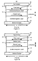
- FIG. 3A depicting a first embodiment of a portion of a magnetic element 100 in accordance with the present invention having a reduced write current density for spin transfer switching.
- the magnetic element 100 is preferably used in a magnetic memory, such as a MRAM, in a CPP configuration.
- the magnetic element 100 may be used in a memory cell including an isolation transistor (not shown), as well as other configurations of magnetic memories.
- the magnetic element 100 preferably utilizes the two terminals 102 and 104 near the top and bottom, respectively, of the magnetic element 100. However, nothing prevents the use of another number of terminals, for example a third terminal near the center of the magnetic element.
- the magnetic element 100 includes a first pinned layer 120, a spacer layer 130, a free layer 140, and a second pinned layer 160.
- the magnetic element 100 generally also includes a first pinning layer 110 and a second pinning layer 170 used to pin the magnetization 122 and 162, respectively, of the pinned layers 120 and 160, respectively, as well as seed layers (not shown) and capping layers (not shown).
- the magnetic element 100 is configured such that the free layer 140 can be written using spin transfer.
- the lateral dimensions, such as the width w, of the free layer 140 are thus small and preferably less than two hundred nanometers.
- some difference is preferably provided between the lateral dimensions to ensure that the free layer 140 has a particular easy axis in the plane of the free layer 140.
- the pinning layers 110 and 170 are preferably AFM layers 110 and 170, respectively, that pin the magnetizations 122 and 162, respectively, of the pinned layers 120 and 160, respectively, through an exchange coupling. Note that although the pinned layer magnetizations 122 and 162 are depicted as being antiparallel, nothing prevents the magnetizations 122 and 162, respectively, from having other orientations. For example, the AFM layer 170 may pin the magnetization 162 of the pinned layer 160 parallel, antiparallel, or perpendicular to the magnetization 122 of the pinned layer 120.
- the pinned layers 120 and 160 are ferromagnetic. In one embodiment the pinned layer 120 and/or the pinned layer 160 are synthetic.
- the pinned layer 120 and/or the pinned layer 160 includes ferromagnetic layers separated by nonmagnetic layers and is configured such that the ferromagnetic layers are aligned antiparallel.
- the pinned layers 120 and/or 160 may have other features used to improve the performance of the magnetic element 100.
- the spacer layer 130 is nonmagnetic.
- the spacer layer 130 may be conductive, for example including Cu.
- the spacer layer 130 is a barrier layer including an insulator such as alumina.
- the barrier layer 130 is configured such that charge carriers can tunnel between the free layer 140 and the pinned layer 120.
- the spacer layer 130 is a current confined layer.
- the spacer layer 130 may correspond to the spacer layers 16, 16', or 16" depicted in Figures 1A, 1B , or 1C , respectively.
- the magnetic element 100 can thus be a current confined magnetoresistance structure.
- the free layer 140 is ferromagnetic. As described above, the free layer 140 preferably has some shape anisotropy such that the magnetization 142 of the free layer 140 is stable when either parallel or antiparallel to the magnetization 122 of the pinned layer 120. Furthermore, the free layer 140 may be simple, as depicted in Figure 3A , or synthetic.
- the magnetic element 100 also includes the spin barrier layer 150 between the free layer 140 and the second pinned layer 160.
- the spin barrier layer 150 can thus also be viewed as acting as a second spacer layer.
- the spin barrier layer 150 is configured to reduce an outer surface contribution to the damping constant, ⁇ , of the free layer.
- the spin barrier layer 150 preferably has a large areal resistance, r b .
- the large areal resistance is at least 0.1 ⁇ . ⁇ m 2 .
- the spin barrier layer 150 is essentially a current confined layer including conductive channels 152 in an insulating matrix 154. Because of the presence of the spin barrier layer 150 that reduces the outer surface contribution to the damping constant, the critical current at which the magnetization 142 of the free layer 140 switches is reduced.
- the effect of the spin barrier layer 150 can be understood using the prevalent spin transfer spin-torque model described above.
- the spin barrier layer 150 is used to alter the outer interface of the free layer 140 and thus reduce the contribution of the outer surface contribution to the damping parameter, ⁇ out , to the total damping parameter. Consequently, the critical current is reduced.
- the critical current I c for the free layer of a spin transfer stack is proportional to ⁇ , the phenomenological Gilbert damping parameter of the free layer 140.
- ⁇ the total damping coefficient
- the intrinsic damping parameter, ⁇ 0 depends upon the material(s) used for the free layer 140, the intrinsic damping parameter is generally unavailable for engineering to reduce the critical current.
- the surface contribution to the damping parameter, ⁇ in depends on the detail of the structure and composition of the interface between the free layer 140 and first spacer layer 130, the first spacer layer 130 itself, possibly the interface between the first spacer layer 130 and the first pinned layer 120, and the first pinned layer 120.
- the composition and structure of these various elements 120, 130, and 140 are generally optimized in regards with various other constraints.
- the free layer 140, first spacer layer 130, and first pinned layer 120 are generally configured to optimize the resistance of that portion of the magnetic element 100 and to adjust the areal resistance of the magnetic element 100 in a desired proper range, as well as other constraints. Consequently, the resulting ⁇ in is generally taken as is.
- the spin barrier layer 150 is used to alter the outer interface of the free layer 140 and thus reduce the contribution of the outer surface contribution to the damping parameter, ⁇ out , to the total damping parameter.
- a reduction in the outer surface contribution to the damping parameter ensures that this contribution, ⁇ out , is less than for the free layer 140 alone.
- the spin barrier layer 150 has a large areal resistance, r b , at least 0.1 ⁇ . ⁇ m 2 .
- r b a large areal resistance
- Such a high areal resistance reduces the coupling between the time dependent magnetization of the free layer 140 and the conduction electrons in the outer electrode 104, across the spin barrier layer 150. Consequently, this coupling may no longer contribute significantly to the damping of the magnetization of the free layer 150.
- the high areal resistance of the spin barrier layer 150 results in an effective cancellation of the spin pumping induced additional damping and, therefore, a reduction in the surface contribution to the damping parameter, ⁇ out . Consequently, a beneficial reduction in the critical current magnitude I o required to switch the free layer magnetization 142 is achieved.
- the dual magnetoresistance element 100 has a further reduced critical current.
- the spin barrier layer 150 is a current confined spin barrier layer.
- the spin barrier layer 150 is a thin layer inhomogeneous across the plane of the layer 150.
- the spin barrier layer 150 thus has areas of metallic (ohmic) conduction, termed conductive channels 152, and areas of high resistivity, termed an insulating matrix 154.
- the insulating matrix 154 may actually be insulating areas or may simply have a resistivity that is high in comparison to the conductive channels 152 As a result, conduction of current through the spin barrier layer 150 is primarily confined to the conductive channels 152 In a magnetic element 100, the areal resistance of the spin barrier layer 150 can be adjusted by varying the size and density of the conductive channels 152 allowing the targeted specification for r b to be met relatively easily.
- the current confined spin barrier layer 150 has a thickness that is preferably between 0.2 and 5 nm.
- the spin barrier layer 150 is made in large part from an oxide of one of more materials selected from a group consisting of Al, B, Si, Ge, W, Nb, Mo, Ta, V, Ti, Cr, Fe, Co, and Ni.
- the conductive channels 152 may correspond to areas of lower atomic concentration in oxygen. In a preferred embodiment to areas of oxygen atomic concentration below thirty percent are considered to be the conductive channels 152.
- the areas of high resistivity, the insulating matrix 154 may correspond to areas of higher atomic concentration in oxygen.
- the insulating matrix 154 corresponds to areas of atomic oxygen concentration above forty percent.
- the lateral fluctuation in oxygen atomic concentration across the spin barrier layer 150 are preferably induced by addition to the spin barrier layer 150 of metallic element(s), or oxygen segregation agent, that does not oxidize easily.
- the conductive channels 152 may include element(s) selected from the group consisting of Cu, Ag, Au, Pt, Pd, Ir, and Os.
- the current confined spin barrier layer 150 preferably has a thickness comprised between 0.2 and 5 nm.
- the spin barrier layer 150 is made in large part from a nitride of elements (the matrix elements) selected from the group consisting of Al, B, Si, Ge, Ti.
- the conductive channels 152 correspond to areas of lower atomic concentration in nitrogen. In a preferred embodiment, the conductive channels 152 correspond to areas of nitrogen atomic concentration below thirty percent.
- the insulating matrix 154 corresponds to areas of high resistivity, preferably where the atomic nitrogen concentration is above forty percent.
- the lateral fluctuations in nitrogen atomic concentration across the spin barrier layer 150 are preferably induced by addition to the spin barrier layer 150 of a metallic element, or the nitrogen segregation agent, that does not react easily with nitrogen.
- a metallic element or the nitrogen segregation agent, that does not react easily with nitrogen.
- element(s) selected from the group consisting of Cu, Ag, Au, Pt, Pd, Ir, and Os.
- a current of between one and five hundred microamperes may be used as the read current.
- I c critical current
- a write current that is at least equal to the critical current, I c is applied in the appropriate direction (i.e. up or down in Figure 3A ) to write to the magnetic element 100.
- the magnetization 142 of the free layer 140 can be switched to be parallel or antiparallel to the magnetization 122 of the pinned layer 120.
- Such a write current may be between ten and two thousand microamperes.
- the spin barrier layer 150 reduces an outer surface contribution to the damping constant, ⁇ , of the free layer.
- the critical current at which the magnetization 142 of the free layer 140 switches is reduced. Consequently, performance of the magnetic element 100 can be improved.
- Figure 3B depicts another version of the first embodiment of a portion of a magnetic element 100' in accordance with the present invention having a reduced write current density for spin transfer switching.
- Components of the magnetic element 100' are analogous to the magnetic element 100. Consequently, portions of the magnetic element 100' are labeled similarly to the magnetic element 100.
- the magnetic element 100' includes a first pinning layer 110' that is preferably an AFM layer, pinned layer 120', a spacer layer 130', a free layer 140', a spin barrier layer 150', a second pinned layer 160', and a second pinning layer 170' that is preferably an AFM layer.
- Current is preferably driven in a CPP configuration using electrodes 102' and 104'.
- the spacer layer 130' may take on various forms, including a conductive layer, a tunneling barrier layer, or a current confined layer.
- the layers of the magnetic element 100' are substantially the same as and function in an analogous manner to the layers of the magnetic element 100.
- the spin barrier layer 150' functions in an analogous manner to the spin barrier layer 150, the structure of the spin barrier layer 150 is different.
- the spin barrier layer 150' is a tunneling barrier that includes a thin insulating, a semiconducting layer, or other analogous layer. Conduction of current through the spin barrier layer 150' is thus allowed by electronic tunneling, electron hoping and/or thermally activated conduction.
- the areal resistance of the spin barrier layer 150' may be adjusted by varying the thickness and composition of the spin barrier layer 150'.
- the targeted specification for r b may be met.
- the spin barrier layer 150' has a thickness between 0.2 and 5 nm. Also in a preferred embodiment, the spin barrier layer is in large part comprised of an oxide of elements selected from the group consisting of Al, B, Si, Ge, W, Nb, Mo, Ta, V, Ti, Cr, Fe, Co, or Ni. In an alternate embodiment of the magnetic element 100', the spin barrier layer 150' has a thickness comprised between 0.2 and 5 nm, and is made in large part from a nitride of element(s) selected from the group consisting of A, B, Si, Ge, Ti. In yet another embodiment, the spin barrier layer 150' is made in large part from a semiconductor material.
- the spin barrier layer 150' preferably has a thickness of between 0.2 and 5 nm.
- the semiconductor material used in such an embodiment is preferably made out of element(s) selected from the group constituted Si, Ge, Ga, Cd, Te, Sb, In, Al, As, Hg, and C.
- the spin barrier layer 150' reduces an outer surface contribution to the damping constant, ⁇ , of the free layer. Because the spin barrier layer 150' reduces the outer surface contribution to the damping constant in a manner analogous to that described above, the critical current at which the magnetization 142' of the free layer 140' switches is reduced. Consequently, performance of the magnetic element 100' can be improved.
- Figure 3C depicts a third version of the first embodiment of a portion of a magnetic element 100" in accordance with the present invention having a reduced write current density for spin transfer switching.
- Components of the magnetic element 100" are analogous to the magnetic element 100. Consequently, portions of the magnetic element 100" are labeled similarly to the magnetic elements 100 and 100'.
- the magnetic element 100" includes a first pinning layer 110" that is preferably an AFM layer, a first pinned layer 120", a spacer layer 130", a free layer 140", a spin barrier layer 150", a second pinned layer 160", and a second pinning layer 170” that is preferably an AFM layer.
- Current is preferably driven in a CPP configuration using electrodes 102" and 104".
- the spacer layer 130" may take on various forms, including a conductive layer, a tunneling barrier layer, or a current confined layer.
- the layers of the magnetic element 100" are substantially the same as and function in an analogous manner to the layers of the magnetic element 100 and 100'.
- the spin barrier layer 150" may be a current confined spin barrier layer, such as the spin barrier layer 150, or a tunneling spin barrier layer, such as the spin barrier layer 150'.
- the spin barrier layer 150 functions in a similar manner to the spin barrier layers 150 and 150'.
- the pinned layers 120" and 160" and the free layer 140" are synthetic. Consequently, the first pinned layer 120" includes ferromagnetic layers 124 and 128 separated by a nonmagnetic spacer layer 126 that is preferably Ru.
- the nonmagnetic spacer layer 126 is configured so that the magnetizations 125 and 127 of the ferromagnetic layers 124 and 128, respectively, are antiferromagnetically coupled.
- the second pinned layer 160" includes ferromagnetic layers 164 and 168 separated by a nonmagnetic spacer layer 166 that is preferably Ru.
- the nonmagnetic spacer layer 166 is configured so that the magnetizations 165 and 167 of the ferromagnetic layers 164 and 168, respectively, are antiferromagnetically coupled.
- the free layer 140" includes ferromagnetic layers 144 and 148 separated by a nonmagnetic spacer layer 146 that is preferably Ru.
- the nonmagnetic spacer layer 146 is configured so that magnetizations 145 and 147 of the ferromagnetic layers 144 and 148, respectively, are antiferromagnetically coupled.
- the spin barrier layer 150' reduces an outer surface contribution to the damping constant, ⁇ , of the free layer.
- the critical current at which the magnetization 142" of the free layer 140" switches is reduced. Consequently, performance of the magnetic element 100" can be improved.
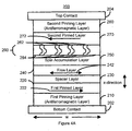
- Figure 4A depicts a second embodiment of a portion of a magnetic element 200 in accordance with the present invention having a reduced write current density for spin transfer.
- the magnetic element 200 is preferably used in a magnetic memory, such as a MRAM, in a CPP configuration.
- the magnetic element 200 may be used in a memory cell including an isolation transistor (not shown), as well as other configurations of magnetic memories.
- the magnetic element 200 preferably utilizes the two terminals 202 and 204 near the top and bottom, respectively, of the magnetic element 200. However, nothing prevents the use of another number of terminals, for example a third terminal near the center of the magnetic element.
- the magnetic element 200 includes a first pinned layer 220, a spacer layer 230, a free layer 240, a spin accumulation layer 250, a spin barrier layer 260, and a second pinned layer 270.
- the magnetic element 200 generally also includes a first pinning layer 210 used to pin the magnetization 222 of the first pinned layer 220, a second pinning layer 280 used to pin the magnetization 272 of the second pinned layer 270, as well as seed layers (not shown) and capping layers (not shown).
- the magnetic element 200 is configured such that the free layer 240 can be written using spin transfer.
- the lateral dimensions, such as the width w, of the free layer 240 are thus small and preferably less than two hundred nanometers.
- some difference is preferably provided between the lateral dimensions to ensure that the free layer 240 has a particular easy axis in the plane of the free layer 240.
- the pinned layers 220 and 280 are ferromagnetic.
- the first pinned layer 220 and/or the second pinned layer 280 are synthetic.
- the first pinned layer 220 and/or the second pinned layer 280 may include ferromagnetic layers separated by nonmagnetic layers and is configured such that the ferromagnetic layers are aligned antiparallel.
- the first pinned layer 220 and/or the second pinned layer 280 may have other features used to improve the performance of the magnetic element 200.
- the spacer layer 230 is nonmagnetic.
- the spacer layer 230 may be conductive, for example including Cu.
- the spacer layer 230 is a barrier layer including an insulator such as alumina.
- the barrier layer 230 is configured such that charge carriers can tunnel between the free layer 240 and the pinned layer 220.
- the spacer layer 230 is a current confined layer.
- the spacer layer 230 may correspond to the spacer layers 16, 16', or 16" depicted in Figures 1A, 1B , or 1C , respectively.
- the magnetic element 200 can thus be a current confined magnetoresistance structure.
- the free layer 240 is ferromagnetic. As described above, the free layer 240 preferably has some shape anisotropy such that the magnetization 242 of the free layer 240 is stable when either parallel or antiparallel to the magnetization 222 of the pinned layer 220. Furthermore, the free layer 240 may be simple, as depicted in Figure 4A , or synthetic.
- the magnetic element 200 also includes the spin accumulation layer 250 and the spin barrier layer 260.
- the combination of the spin accumulation layer 250 and the spin barrier layer 260 is used to alter the outer interface of the free layer 240 and thus reduce the contribution of the outer surface contribution to the damping parameter, ⁇ out , to the total damping parameter.
- the spin accumulation layer 250 in combination with the spin barrier layer 260 reduce an outer surface contribution to the damping constant, ⁇ , of the free layer.
- the critical current at which the magnetization 242" of the free layer 240" switches is reduced. Consequently, performance of the magnetic element 200" can be improved.
- the function of the spin accumulation layer 250 and the spin barrier layer 260 may be explained as follows.
- the spin accumulation layer 250 is metallic (e.g. has a high conductivity). Also in a preferred embodiment, the spin accumulation layer 250 has a very long spin flip scattering time, or equivalently a long spin diffusion length. In a preferred embodiment of the invention, the spin accumulation layer 250 is thus made of a very pure, of relatively small atomic weight, and highly conductive metal, such as Al, Cu, or Ag known to exhibit very long spin diffusion length. A typical value for the "long" spin diffusion length in such metal layer at room temperature is above forty nanometers.
- the spin accumulation layer has a thickness between 0.5 nm and 5 nm, which is much smaller than the spin diffusion length in the spin accumulation layer. Because of the very long spin diffusion length of the spin accumulation layer 250, the angular momentum transferred into the spin accumulation layer 250 by spin pumping from the time dependent magnetization of the free layer 240 is long lived, and can accumulate. As a result, there is some nonzero probability for this accumulated angular momentum to be transported outward toward the spin barrier layer 260. Similarly, there is some nonzero probability that this accumulated angular momentum to be transported inward back into the free layer 240.
- the spin barrier layer 260 is analogous to the spin barrier layers 150, 150', and 150" and thus functions similarly.
- the spin barrier layer 260 preferably has a large areal resistance, r b .
- the areal resistance of the spin barrier layer 260 expressed in ⁇ . ⁇ m 2 , is sufficiently large that the dimensionless product g r ⁇ r b is larger than ten.
- the quantity g r ⁇ is the spin mixing conductance of the interface between the free layer 240 and the spin accumulation layer 250, expressed in ⁇ -1 . ⁇ m -2 .
- the spin mixing conductance has been defined in the context of the magneto-electronic theory of magnetoresistance effect film structures, as explained in details in: " Spin torques in ferromagnetic/metal structures", by K. Xia et al., Phys. Rev. B 65, 220401(R) (2002 ). Typical values of the spin mixing conductance for metal/metal interface in the range of one hundred to one thousand ⁇ -1 . ⁇ m -2 . Consequently, in a preferred embodiment of the invention, the spin barrier layer 260 has an areal resistance larger than 0.01 ⁇ . ⁇ m 2 , and possibly larger than 0.1 ⁇ . ⁇ m 2 , to achieve the dimensionless product of approximately ten.
- the probability for the angular momentum accumulated in the spin accumulation layer 250 to be transported inward back into the magnetic free layer 240 becomes much larger than the probability to be transferred outward through the spin barrier layer 260. Stated differently, it becomes significantly more likely that angular momentum accumulated in the spin accumulation layer 250 will be returned to the free layer 240. This results in an effective cancellation of the spin pumping induced additional damping and, therefore, a reduction in the outer surface contribution to the damping parameter, ⁇ out . Consequently, in a beneficial reduction in the critical current magnitude I c to switch the free layer 240 magnetization is achieved.
- the spin barrier layer 260 is essentially a current confined layer.
- the spin barrier layer 260 is analogous to the spin barrier layer 150 depicted in Figure 3A .
- the spin barrier layer 260 is a thin layer inhomogeneous across the plane of the layer 260.
- the spin barrier layer 260 thus has areas of metallic (ohmic) conduction, termed conductive channels 262, and areas of high resistivity, termed an insulating matrix 264.
- the insulating matrix 264 may actually be insulating areas or may simply have a resistivity that is high in comparison to the conductive channels 264.
- conduction of current through the spin barrier layer 260 is primarily confined to the conductive channels 264.
- the areal resistance of the spin barrier layer 260 can be adjusted by varying the size and density of the conductive channels 264, allowing the targeted specification for r b to be met relatively easily.
- the current confined spin barrier layer 260 has a thickness that is preferably between 0.2 and 5 nm.
- the spin barrier layer 260 is made in large part from an oxide of one of more materials selected from a group consisting of Al, B, Si, Ge, W, Nb, Mo, Ta, V, Ti, Cr, Fe, Co, and Ni.
- the conductive channels 262 may correspond to areas of lower atomic concentration in oxygen. In a preferred embodiment to areas of oxygen atomic concentration below thirty percent are considered to be the conductive channels 262.
- the areas of high resistivity, the insulating matrix 264 may correspond to areas of higher atomic concentration in oxygen.
- the insulating matrix 264 corresponds to areas of atomic oxygen concentration above forty percent.
- the lateral fluctuation in oxygen atomic concentration across the spin barrier layer 260 are preferably induced by addition to the spin barrier layer 260 of metallic element(s), or oxygen segregation agent, that does not oxidize easily.
- the conductive channels 262 may include element(s) selected from the group consisting of Cu, Ag, Au, Pt, Pd, Ir, and Os.
- the current confined spin barrier layer 260 preferably has a thickness comprised between 0.2 and 5 nm.
- the spin barrier layer 260 is made in large part from a nitride of elements (the matrix elements) selected from the group consisting of Al, B, Si, Ge, Ti.
- the conductive channels 262 correspond to areas of lower atomic concentration in nitrogen. In a preferred embodiment, the conductive channels 262 correspond to areas of nitrogen atomic concentration below thirty percent.
- the insulating matrix 264 corresponds to areas of high resistivity, preferably where the atomic nitrogen concentration is above forty percent.
- the lateral fluctuations in nitrogen atomic concentration across the spin barrier layer 260 are preferably induced by addition to the spin barrier layer 260 of a metallic element, or the nitrogen segregation agent, that does not react easily with nitrogen.
- a metallic element or the nitrogen segregation agent, that does not react easily with nitrogen.
- element(s) selected from the group consisting of Cu, Ag, Au, Pt, Pd, Ir, and Os.
- a current of between one and five hundred microamperes may be used as the read current.
- a read current allows the state of the magnetic element 200 to be determined yet does not result in spin transfer induced switching of the free layer 240.
- a write current that is at least equal to the critical current, I c is applied in the appropriate direction (i.e. up or down in Figure 4A ) to write to the magnetic element 200.
- the magnetization 242 of the free layer 240 can be switched to be parallel or antiparallel to the magnetization 222 of the pinned layer 220.
- Such a write current may be between ten and two thousand microamperes.
- the combination of the spin accumulation layer 250 that accumulates spin angular momentum, and spin barrier layer 260 that allows the accumulated spin angular momentum to have a higher probability of returning to the free layer 240 helps reduce an outer surface contribution to the damping constant, ⁇ , of the free layer. As a result, the critical current at which the magnetization 242 of the free layer 240 switches is reduced. Consequently, performance of the magnetic element 200 can be improved.
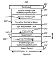
- Figure 4B depicts another version of the second embodiment of a portion of a magnetic element 200' in accordance with the present invention having a reduced write current density for spin transfer switching.
- Components of the magnetic element 200' are analogous to the magnetic element 200. Consequently, portions of the magnetic element 200' are labeled similarly to the magnetic element 200.
- the magnetic element 200' includes a first pinning layer 210' that is preferably an AFM layer, a first pinned layer 220', a spacer layer 230', a free layer 240', a spin accumulation layer 250', a spin barrier layer 260', a second pinned layer 270', and a second pinning layer 280' that is preferably an AFM layer.
- the spacer layer 230' may take on various forms, including a conductive layer, a tunneling barrier layer, or a current confined layer.
- the layers of the magnetic element 200' are substantially the same as and function in an analogous manner to the layers of the magnetic element 200.
- the spin barrier layer 260' is a tunneling barrier that includes a thin insulating, a semiconducting layer, or other analogous layer. Conduction of current through the spin barrier layer 260' is thus allowed by electronic tunneling, electron hoping and/or thermally activated conduction. In such a magnetic element 200', the areal resistance of the spin barrier layer 260' may be adjusted by varying the thickness and composition of the spin barrier layer 260'. Thus, the targeted specification for r b may be met.
- the spin barrier layer 260' has a thickness between 0.2 and 5 nm.
- the spin barrier layer is in large part comprised of an oxide of elements selected from the group consisting of Al, B, Si, Ge, W, Nb, Mo, Ta, V, Ti, Cr, Fe, Co, or Ni.
- the spin barrier layer 260' has a thickness between 0.2 and 5 nm, and is made in large part from a nitride of element(s) selected from the group consisting of A, B, Si, Ge, Ti.
- the spin barrier layer 260' is made in large part from a semiconductor material.
- the spin barrier layer 260' preferably has a thickness of between 0.2 and 5 nm.
- the semiconductor material used in such an embodiment is preferably made out of element(s) selected from the group constituted Si, Ge, Ga, Cd, Te, Sb, In, Al, As, Hg, and C.
- the combination of the spin accumulation layer 250' and the spin barrier layer 260' reduces an outer surface contribution to the damping constant, ⁇ , of the free layer 240' in a manner similar to that described above with respect to Figure 4A . Because the spin accumulation layer 250' with the spin barrier layer 260' reduces the outer surface contribution to the damping constant in a manner analogous to that described above, the critical current at which the magnetization 242' of the free layer 240' switches is reduced. Consequently, performance of the magnetic element 200' can be improved.
- Figure 4C depicts a third version of the second embodiment of a portion of a magnetic element 200" in accordance with the present invention having a reduced write current density for spin transfer switching.
- Components of the magnetic element 200" are analogous to the magnetic element 200. Consequently, portions of the magnetic element 200" are labeled similarly to the magnetic elements 300 and 200'.
- the magnetic element 200" includes a first pinning layer 210" that is preferably an AFM layer, a first pinned layer 220", a spacer layer 230", a free layer 240", a spin accumulation layer 250', a spin barrier layer 260", a second pinned layer 270", and a second pinning layer 280" that is preferably an AFM layer.
- the spacer layer 230" may take on various forms, including a conductive layer, a tunneling barrier layer, or a current confined layer.
- the layers of the magnetic element 200" are substantially the same as and function in an analogous manner to the layers of the magnetic element 200 and 200'.
- the spin barrier layer 260" may be a current confined spin barrier layer, such as the spin barrier layer 250, or a tunneling spin barrier layer, such as the spin barrier layer 250'.
- the spin barrier layer 260" in combination with the spin accumulation layer 250” functions in a similar manner to the spin barrier layers 250 and 250'.
- the first pinned layer 220", the free layer 240", and the second pinned layer 270" are synthetic. Consequently, the pinned layer 220" includes ferromagnetic layers 224 and 228 separated by a nonmagnetic spacer layer 226 that is preferably Ru.
- the nonmagnetic spacer layer 226 is configured so that the magnetizations 225 and 227 of the ferromagnetic layers 224 and 228, respectively, are antiferromagnetically coupled.
- the pinned layer 270" includes ferromagnetic layers 274 and 278 separated by a nonmagnetic spacer layer 276 that is preferably Ru.
- the nonmagnetic spacer layer 276 is configured so that the magnetizations 275 and 277 of the ferromagnetic layers 274 and 278, respectively, are antiferromagnetically coupled.
- the free layer 240" includes ferromagnetic layers 244 and 248 separated by a nonmagnetic spacer layer 246 that is preferably Ru.
- the nonmagnetic spacer layer 246 is configured so that magnetizations 245 and 247 of the ferromagnetic layers 244 and 248, respectively, are antiferromagnetically coupled.
- the spin barrier layer 260"-spin accumulation layer 250" combination reduces an outer surface contribution to the damping constant, ⁇ , of the free layer 240.
- the critical current at which the magnetization 242" of the free layer 240" switches is reduced. Consequently, performance of the magnetic element 200" can be improved.
- the critical current to switch the magnetization direction for the corresponding free layer 130, 130', 130", 230, 230', and 230" is reduced. Consequently, improved power consumption as well as the remaining benefits of lower I c can be achieved.
- Figure 5 depicts a flow chart of an example of a method in accordance with the present invention for providing one embodiment of a magnetic element in accordance with the present invention.
- the method 600 is described in the context of the magnetic elements 100, 100', 100", 200, 200', and 200".
- a first pinned layer such as the pinned layer 120, 120', 120", 220, 220', and/or 220" is provided, via step 302.
- step 302 includes providing a synthetic pinned layer.
- the spacer layer 130, 130', 130", 230, 230', and/or 230" is provided, via step 304.
- Step 304 can include providing a barrier layer, a conducting layer, or a current confined layer.
- step 306 The free layer 140, 140', 140", 240,240', and/or 240" is provided, via step 306.
- the spin accumulation layer 240, 240', or 240" is optionally provided, depending upon the embodiment being fabricated, via step 308.
- step 308 includes sputtering the spin accumulation layer 250,250, or 250" in a high vacuum deposition chamber from a high purity metal target.
- the spin barrier layer 150, 150', 150", 260, 260', and/or 260" is provided, via step 310.
- step 310 can be used to form the spin diffusion layers 150 or 250.
- step 310 includes alternate co-sputtering the selected matrix element(s) in a high vacuum deposition chamber of sub-monolayers from a high purity target of the selected matrix element(s) with a high purity target of the selected oxygen segregation agent.
- the co-sputtering is tuned such that the selected proportions and the selected total thickness can be achieved. In such an embodiment, deposition would be followed by natural oxidation.
- step 310 includes alternate reactive co-sputtering in a high vacuum deposition chamber sub-monolayers from a high purity target of the selected matrix element(s) and from a high purity target of the selected nitrogen segregation agent. The co-sputtering is tuned so that the selected proportions and the selected total thickness can be achieved.
- step 310 provides a tunneling layer 150' or 260' by sputtering in a high vacuum deposition chamber from a high purity target of the selected matrix element(s), followed by natural oxidation in a rarefied atmosphere of pure oxygen.
- reactive sputtering in a high vacuum deposition chamber from a high purity target of the selected matrix element(s), using a mixture of argon and nitrogen as a sputtering gas can be used.
- Yet another tunnel spin barrier layer 150' or 160' can be provided by sputtering in a high vacuum deposition chamber from a high purity target of the selected semiconductor material.
- the second pinned layer such as the pinned layer 160, 160', 160", 270, 270', and/or 270" is provided, via step 312.
- the remaining portion(s) of the magnetic element and corresponding magnetic memory (not explicitly shown).
- the magnetic elements 100. 100', 100", 200, 200', 200" may be provided.
Landscapes
- Engineering & Computer Science (AREA)
- Computer Hardware Design (AREA)
- Chemical & Material Sciences (AREA)
- Nanotechnology (AREA)
- Crystallography & Structural Chemistry (AREA)
- Hall/Mr Elements (AREA)
- Mram Or Spin Memory Techniques (AREA)
Description
- The present invention relates to a magnetic element that employs a spin transfer effect in switching and that can be switched using a lower switching current density.
-
Figures 1A, 1B , and1C depict conventionalmagnetic elements magnetic element 10 is a spin valve and includes a conventional antiferromagnetic (AFM)layer 12, a conventional pinnedlayer 14, aconventional spacer layer 16 that is conductive and a conventionalfree layer 18. Other layers (not shown), such as seed or capping layer may also be used. The conventional pinnedlayer 14 and the conventionalfree layer 18 are ferromagnetic. Thus, the conventionalfree layer 18 is depicted as having achangeable magnetization 19. Theconventional spacer layer 16 is nonmagnetic. TheAFM layer 12 is used to fix, or pin, the magnetization of thepinned layer 14 in a particular direction. The magnetization of thefree layer 18 is free to rotate, typically in response to an external magnetic field. Also depicted aretop contact 20 andbottom contact 22 that can be used to drive current through the conventionalmagnetic element 10. - The conventional magnetic element 10' depicted in
Figure 1B is a spin tunneling junction. Portions of the conventional spin tunneling junction 10' are analogous to theconventional spin valve 10. Thus, the conventional magnetic element 10' includes an AFM layer 12', a conventional pinned layer 14', a conventional space layer that is an insulating barrier layer 16' and a conventional free layer 18' having a changeable magnetization 19'. The conventional barrier layer 16' is thin enough for electrons to tunnel through in a conventional spin tunneling junction 10'. - The conventional
magnetic element 10" includes an AFM layer 12', a conventional pinned layer 14', a conventional spacer layer that is a current confinedlayer 16" and a conventionalfree layer 18" having achangeable magnetization 19". The conventional current confinedlayer 16" is an inhomogeneous layer mixing areas of metallic conduction (hereafter termed conductive channels 15), with high resistivity regions (hereafter termed an insulating matrix 17) that may be insulators. The conduction between theferromagnetic layers 14" and 18" is essentially confined to theconductive channels 15. The conventionalmagnetic element 10" is thus termed a current confined magnetoresistance effect thin film structure. The conventionalmagnetic element 10" is more fully described in the context of magnetoresistive hard disk drive read-out heads in: "The Applicability of CPP-GMR Heads for Magnetic Recording", by M. Takagishi et al., IEEE Trans. Magn. 38, 2277 (2002). - Depending upon the orientations of the
magnetization 19/19'/19" of the conventionalfree layer 18/18'/18" and the conventionalpinned layer 14/14'/14", respectively, the resistance of the conventionalmagnetic element 10/10'/10", respectively, changes. When themagnetization 19/19'/19" of the conventionalfree layer 18/18'/18" is parallel to the magnetization of the conventionalpinned layer 14/14'/14", the resistance of the conventionalmagnetic element 10/10'/10" is low. When themagnetization 19/19'/19" of the conventionalfree layer 18/18'/18" is antiparallel to the magnetization of the conventionalpinned layer 14/14'/14", the resistance of the conventionalmagnetic element 10/10'/10" is high. To sense the resistance of the conventionalmagnetic element 10/10'/10", current is driven through the conventionalmagnetic element 10/10'/10". Typically in memory applications, current is driven in a CPP (current perpendicular to the plane) configuration, perpendicular to the layers of conventionalmagnetic element 10/10'/10" (up or down, in the z-direction as seen inFigure 1A, 1B , or1C ). In this configuration, current is driven between thetop contact bottom contact - In order to overcome certain issues associated with magnetic memories having a higher density of memory cells, spin transfer may be utilized to switch the
magnetizations 19/19'/19" of the conventionalfree layers 10/10'/10". Spin transfer is described in the context of the conventional magnetic element 10', but is equally applicable to the conventionalmagnetic elements - When a spin-polarized current traverses a magnetic multilayer such as the spin tunneling junction 10' in a CPP configuration, a portion of the spin angular momentum of electrons incident on a ferromagnetic layer may be transferred to the ferromagnetic layer. In particular, electrons incident on the conventional free layer 18' may transfer a portion of their spin angular momentum to the conventional free layer 18'. This transfer of angular momentum can be considered a spin transfer torque acting on the free layer magnetization 19'. As a result, a spin-polarized current can switch the magnetization 19' direction of the conventional free layer 18' if the current density is sufficiently high (approximately 107-108 A/cm2) and the lateral dimensions of the spin tunneling junction are small (approximately less than two hundred nanometers). The threshold current at which spin transfer induced switching can occur is termed the critical current, Ic. In addition, for spin transfer to be able to switch the magnetization 19' direction of the conventional free layer 18', it is generally believed that the conventional free layer 18' should be sufficiently thin, for instance, preferably less than approximately ten nanometers for Co. Spin transfer based switching of magnetization dominates over other switching mechanisms and becomes observable when the lateral dimensions of the conventional magnetic element 10' are small, in the range of few hundred nanometers. Consequently, spin transfer is suitable for higher density magnetic memories having smaller magnetic elements 10'.
- The phenomenon of spin transfer can be used in the CPP configuration as an alternative to or in addition to using an external switching field to switch the direction of magnetization of the conventional
free layer 18/18'/18" of the conventionalmagnetic element 10/10'/10". For example, in the conventional magnetic element 10', the magnetization 19' of the conventional free layer 18' can be switched from antiparallel to the magnetization of the conventional pinned layer 14' to parallel to the magnetization of the conventional pinned layer 14'. Current is driven from the conventional free layer 18' to the conventional pinned layer 14' (conduction electrons traveling from the conventional pinned layer 14' to the conventional free layer 18'). Alternatively, the magnetization of the free layer 18' can be switched from a direction parallel to the magnetization of the conventional pinned layer 14' to antiparallel to the magnetization of the conventional pinned layer 14' when current is driven from the conventional pinned layer 14' to the conventional free layer 18' (conduction electrons traveling in the opposite direction. - The magnitude of the critical current, Ic, can be determined using the prevalent spin transfer spin-torque model described in J.C. Slonczewski, "Current-driven Excitation of Magnetic Multilayers," Journal of Magnetism and Magnetic Materials, vol. 159, p. L1-L5 (1996), and further expanded in particular in: "Field dependence of magnetization reversal by spin transfer", by J. Grollier et al., Phys. Rev. B 67, 174402 (2003). According to Slonczewski's model, the switching current density Ic for the free layer of a spin transfer stack is proportional to:

where: - α =
- the phenomenological Gilbert damping parameter;
- t =
- the thickness of the free layer;
- Ms =
- saturation magnetization of the free layer;
- Heff =
- effective field for the free layer;
- g(θ)
- reflects the spin-transfer efficiency
- Thus, the critical current Ic is proportional to the Gilbert damping parameter α of the conventional free layer 18'. This is believed to be equally applicable to spin transfer in conventional spin valve magnetoresistance effect element such as 10 and conventional current confined
magnetoresistance effect element 10". The Gilbert damping parameter α is a dimensionless parameter, which quantifies the level of dynamic damping experienced by the conventional free layer magnetization 18'. Assuming the remaining factors remain the same, a reduction in α results in a proportional reduction of Ic, while an increase in α results in a proportional increase of Ic. For a thin conventional magnetic free layer 18' embedded in a multilayer structure, it has been shown that the total damping coefficient, α, can be in general broken into three contributions:
where: - α0 =
- the intrinsic damping parameter;
- δαout =
- surface contribution originating from processes taking place at the outer interface of the free layer, for example between the conventional free layer 18' and the top contact 20';
- δαin =
- surface contribution originating from processes taking place at the inner interface of the free layer, for example between the conventional free layer 18' and the barrier layer 16';
- t0 =
- arbitrary scaling length;
- tf =
- thickness of the free layer expressed in nanometers
- The inner surface contribution to the damping parameter, δαin, depends on the detail of the structure and composition of the interface between the conventional free layer 18' and conventional barrier layer 16', the conventional barrier layer 16' itself, possibly the interface between the conventional barrier layer 16' and the conventional pinned layer 14', and the conventional pinned layer 14'. In particular, the magnetic element 10' may experience a significant and detrimental contribution of δαout that can be traced back to "spin pumping" taking place at the top (outer) interface of the free layer 10'. Spin pumping damping is generated by losses of angular momentum from the time dependent magnetization of the conventional free layer 18' by exchange coupling with the free electrons able to leave the free layer into the top contact 20'. Such effects are described in details for example in: "Dynamic stiffness of spin valves" Y. Tserkovnyak et al., Phys. Rev. B 67, 140404(R) (2003). Such spin pumping induced damping is a limiting factor in the ability to decrease Ic to desirable levels for magnetoresistance effect thin film structures as known in the prior art, with free layer thickness typically ranging from one to five nanometers.
- Thus, although spin transfer functions as a mechanism for switching the conventional
magnetic elements 10/10'/10", one of ordinary skill in the art will readily recognize that a high current density is typically required to induce switching for the conventionalmagnetic elements 10/10'/10". In particular, the switching current density is on the order of a few 107 A/cm2 or greater. Thus, a high write current is used to obtain the high switching current density. The high operating current leads to design problems for high density MRAM, such as heating, high power consumption, large transistor size, as well as other issues. - One of ordinary skill in the art will readily recognize that one mechanism for reducing the switching current is to employ a dual magnetoresistive element.
Figure 2 depicts a conventionaldual magnetoresistance element 50. Thedual magnetoresistance element 50 includes anAFM layer 52, a first conventional pinnedlayer 54, a firstconventional spacer layer 56, a conventionalfree layer 58, a secondconventional spacer layer 60, a second conventional pinnedlayer 62, and asecond AFM layer 64. Other layers (not shown), such as seed or capping layer may also be used. Abottom contact 66 and atop contact 68 are also shown. The conventional pinnedlayers free layer 58 are ferromagnetic. Thus, the conventionalfree layer 58 is depicted as having achangeable magnetization 59. The conventional spacer layers 56 and 60 are nonmagnetic. Theconventional spacer layer layers 16, 16', and/or 16" depicted inFigures 1A-1C . Referring back toFigure 2 , the AFM layers 52 and 64 are used to fix, or pin, the magnetization of the pinnedlayer 54 in a particular direction. The magnetization of thefree layer 58 is free to rotate, typically in response to an external magnetic field. - When a spin-polarized current traverses the conventional
magnetic element 50, themagnetization 59 of thefree layer 58 can be switched using spin transfer. Angular momentum is carried by the electrical current between the first conventional pinnedlayer 54 and the conventionalfree layer 58. This current generates a first spin transfer torque, T1, that acts on the conventionalfree layer 58. Angular momentum is also carried by the electric current between the second conventional pinnedlayer 62 and the conventionalfree layer 58. This current generates a second spin transfer torque, T2, that also acts on the conventionalfree layer 58. With proper choices of the layer thicknesses, composition, and magnetization orientation of the pinned layers 54 and 62, it is possible to create a conventionalmagnetic element 50 in which the two torques T1 and T2 add in the desired fashion. As a result, a significant reduction in the critical current Ic might be obtained. - Although the critical current, Ic, can be reduced, one of ordinary skill in the art will readily recognize that such conventional
magnetic elements 50 can suffer from drawbacks that adversely affect the performances of the conventionalmagnetic element 50 and magnetic memory that can eventually be built out of it. - First, presume that the second
conventional spacer layer 60 is a conductor. As discussed above, the critical current Ic is proportional to the Gilbert damping parameter α of the conventionalfree layer 58. As indicated above, α can be broken into α0, δαout, and δαin. A conventionalmagnetic element 50 utilizing a secondconventional spacer layer 60 that is metallic experiences a significant and detrimental additional contribution from δαout that can be traced back to "spin pumping" taking place at the top interface of thefree layer 58 in conjunction with the second magnetic pinnedlayer 62. Such "spin pumping" is analogous to the spin pumping described above. - If the second
conventional spacer layer 60 is a tunnel barrier, "spin pumping" at the interface between thefree layer 58 and the second nonconventional spacer layer 60 does not adversely affect the critical current. However, one of ordinary skill in the art will readily recognize that in order for the sub-structure composed of thefree layer 58, the firstconventional spacer layer 56, and the first conventional pinnedlayer 54 to maximize the magnetoresistance effect of the conventionalmagnetic element 50, the firstconventional spacer layer 56 is also a tunnel barrier and that the areal resistance of thesecond spacer layer 60 is significantly smaller than the areal resistance of thefirst tunnel barrier 56. In such a conventional dualspin tunneling junction 50, the areal resistance of the secondconventional spacer layer 60 is typically ten times smaller than the areal resistance of the firstconventional spacer layer 56. Furthermore, for the conventionalmagnetic element 50 to be capable of being written to using spin transfer, even the firstconventional spacer layer 56 has a relatively small areal resistance, typically below twenty Ω.µm2. To manufacture such a conventionalmagnetic element 50 including twotunneling barriers - Finally, if the second
conventional spacer layer 60 is a current confined layer and if the areal resistance of the interface between the conventionalfree layer 58 and the secondconventional spacer layer 60 is larger than 0.1 µm2 , then it can be shown that the spin pumping contribution to the dynamic damping for the conventionalfree layer 58 is effectively suppressed. However, for conventional values of the various material and geometrical parameters defining such a conventionalmagnetic element 50, it can be determined using the magneto-electronic circuit theory that the overall spin transfer torque created on the conventionalfree layer 58 for a given current I flowing between the twocontact electrodes Figures 1A-1C . One can find a detailed description of the magneto-electronic circuit theory, and some of it's applications to spin transfer in the following publication: A. Brataas, Y. V. Nazarov, and G. E. W. Bauer, "Finite-Element Theory of Transport in Ferromagnet- Normal Metal Systems", in Phys. Rev. Lett. 84, 2481 (2000). It is thus desirable to create improved dual magnetoresistance effect thin film structures that exhibits even larger spin transfer torque on the conventionalfree layer 58 for the same current. -
US2004/0061154 discloses a method and system for providing a magnetic element capable of being written using spin-transfer effect while being thermally stable and a magnetic memory using the magnetic element. - Accordingly, what is needed is a system and method for providing a dual magnetoresistance element that can be switched using spin transfer at a lower current and that consumes less power. The present invention addresses such a need.
- The present invention is defined according to claim 1.
- The present invention provides a magnetic element that can be switched due to spin transfer using a lower current density and the attendant advantages of a lower switching current density.
-
-
Figure 1A is a diagram of a conventional magnetic element, a conventional spin valve. -
Figure 1B is a diagram of another conventional magnetic element, a conventional spin tunneling junction. -
Figure 1C is a diagram of a third conventional magnetic element, a conventional current confined magnetoresistance effect thin film structure. -
Figure 2 is a diagram of a conventional dual magnetoresistance magnetic element. -
Figure 3A depicts a first embodiment of a portion of a magnetic element in accordance with the present invention having a reduced write current density for spin transfer switching. -
Figure 3B depicts another version of the first embodiment of a portion of a magnetic element in accordance with the present invention having a reduced write current density for spin transfer switching. -
Figure 3C depicts a third version of the first embodiment of a portion of a magnetic element in accordance with the present invention having a reduced write current density for spin transfer switching. -
Figure 4A depicts a second embodiment of a portion of a magnetic element in accordance with the present invention having a reduced write current density for spin transfer switching. -
Figure 4B depicts another version of the second embodiment of a portion of a magnetic element in accordance with the present invention having a reduced write current density for spin transfer switching. -
Figure 4C depicts a third version of the second embodiment of a portion of a magnetic element in accordance with the present invention having a reduced write current density for spin transfer switching. -
Figure 5 depicts a flow chart of an example of a method in accordance with the present invention for providing one embodiment of a magnetic element in accordance with the present invention having a reduced write current density for spin transfer switching. - The present invention relates to an improvement in magnetic elements and magnetic memories, such as MRAM. The following description is presented to enable one of ordinary skill in the art to make and use the invention and is provided in the context of a patent application and its requirements. Various modifications to the preferred embodiments will be readily apparent to those skilled in the art and the generic principles herein may be applied to other embodiments. Thus, the present invention is not intended to be limited to the embodiments shown, but is to be accorded the widest scope consistent with the principles and features described herein.
- The present invention provides a system for providing a magnetic element that can be used in a magnetic memory. The magnetic element includes first pinned, spacer, free, spin barrier, and second pinned layers. The spacer layer is nonmagnetic and resides between the pinned and free layers. The free layer can be switched using spin transfer when a write current is passed through the magnetic element. The free layer resides between the spacer layer and the spin barrier layer. The spin barrier layer is between the free layer and the second pinned layer. The spin barrier layer is configured to reduce an outer surface contribution to a damping constant of the free layer. In one aspect, the spin barrier layer has a high areal resistance and may substantially eliminate spin pumping induced damping. In another aspect, the magnetic element also includes a spin accumulation layer between the spin barrier and free layers. The spin accumulation layer is metallic (e.g. has a high conductivity), and may have a long spin diffusion length.
- The present invention will be described in terms of a particular magnetic memory and a particular magnetic element having certain components. However, one of ordinary skill in the art will readily recognize that this system will operate effectively for other magnetic memory elements having different and/or additional components and/or other magnetic memories having different and/or other features not inconsistent with the present invention. The present invention is also described in the context of current understanding of the spin transfer phenomenon. Consequently, one of ordinary skill in the art will readily recognize that theoretical explanations of the behavior of the method and system are made based upon this current understanding of spin transfer. One of ordinary skill in the art will also readily recognize that the method and system are described in the context of a structure having a particular relationship to the substrate. For example, as depicted in the drawings, the bottoms of the structures are typically closer to an underlying substrate than the tops of the structures. However, one of ordinary skill in the art will readily recognize that the method and system are consistent with other structures having different relationships to the substrate. In addition, the method and system are described in the context of certain layers being synthetic and/or simple. However, one of ordinary skill in the art will readily recognize that the layers could have another structure. For example, although the system are described in the context of simple free layers, nothing prevents the present invention from being used with synthetic free layers. Furthermore, the present invention is described in the context of magnetic elements having particular layers. However, one of ordinary skill in the art will readily recognize that magnetic elements having additional and/or different layers not inconsistent with the present invention could also be used. Moreover, certain components are described as being ferromagnetic. However, as used herein, the term ferromagnetic could include ferrimagnetic or like structures. Thus, as used herein, the term "ferromagnetic" includes, but is not limited to ferromagnets and ferrimagnets. The present invention is also described in the context of single elements. However, one of ordinary skill in the art will readily recognize that the present invention is consistent with the use of magnetic memories having multiple elements, bit lines, and word lines. The present invention is also described in the context of a particular mechanism, a reduced damping constant for the free layer, for providing a lower switching current density. However, one of ordinary skill in the art will readily recognize that the method and system described herein can be combined with other mechanisms for reducing the switching current density, such as a low saturation magnetization free layer.
- To more particularly illustrate the system in accordance with the present invention, refer now to
Figure 3A , depicting a first embodiment of a portion of amagnetic element 100 in accordance with the present invention having a reduced write current density for spin transfer switching. Themagnetic element 100 is preferably used in a magnetic memory, such as a MRAM, in a CPP configuration. Thus, themagnetic element 100 may be used in a memory cell including an isolation transistor (not shown), as well as other configurations of magnetic memories. Moreover, themagnetic element 100 preferably utilizes the twoterminals magnetic element 100. However, nothing prevents the use of another number of terminals, for example a third terminal near the center of the magnetic element. Themagnetic element 100 includes a first pinnedlayer 120, aspacer layer 130, afree layer 140, and a second pinnedlayer 160. Themagnetic element 100 generally also includes a first pinninglayer 110 and a second pinninglayer 170 used to pin themagnetization layers magnetic element 100 is configured such that thefree layer 140 can be written using spin transfer. In a preferred embodiment, the lateral dimensions, such as the width w, of thefree layer 140 are thus small and preferably less than two hundred nanometers. In addition, some difference is preferably provided between the lateral dimensions to ensure that thefree layer 140 has a particular easy axis in the plane of thefree layer 140. - The pinning
layers magnetizations layers magnetizations AFM layer 170 may pin themagnetization 162 of the pinnedlayer 160 parallel, antiparallel, or perpendicular to themagnetization 122 of the pinnedlayer 120. The pinned layers 120 and 160 are ferromagnetic. In one embodiment the pinnedlayer 120 and/or the pinnedlayer 160 are synthetic. In such an embodiment, the pinnedlayer 120 and/or the pinnedlayer 160 includes ferromagnetic layers separated by nonmagnetic layers and is configured such that the ferromagnetic layers are aligned antiparallel. The pinned layers 120 and/or 160 may have other features used to improve the performance of themagnetic element 100. Thespacer layer 130 is nonmagnetic. In one embodiment, thespacer layer 130 may be conductive, for example including Cu. In another embodiment, thespacer layer 130 is a barrier layer including an insulator such as alumina. In such an embodiment, thebarrier layer 130 is configured such that charge carriers can tunnel between thefree layer 140 and the pinnedlayer 120. In another embodiment thespacer layer 130 is a current confined layer. Thus, thespacer layer 130 may correspond to the spacer layers 16, 16', or 16" depicted inFigures 1A, 1B , or1C , respectively. Referring back toFigure 3A , themagnetic element 100 can thus be a current confined magnetoresistance structure. - The
free layer 140 is ferromagnetic. As described above, thefree layer 140 preferably has some shape anisotropy such that themagnetization 142 of thefree layer 140 is stable when either parallel or antiparallel to themagnetization 122 of the pinnedlayer 120. Furthermore, thefree layer 140 may be simple, as depicted inFigure 3A , or synthetic. - The
magnetic element 100 also includes thespin barrier layer 150 between thefree layer 140 and the second pinnedlayer 160. Thespin barrier layer 150 can thus also be viewed as acting as a second spacer layer. Thespin barrier layer 150 is configured to reduce an outer surface contribution to the damping constant, α, of the free layer. Thespin barrier layer 150 preferably has a large areal resistance, rb. In a preferred embodiment, the large areal resistance is at least 0.1 Ω. µm2. In the embodiment shown, thespin barrier layer 150 is essentially a current confined layer includingconductive channels 152 in an insulatingmatrix 154. Because of the presence of thespin barrier layer 150 that reduces the outer surface contribution to the damping constant, the critical current at which themagnetization 142 of thefree layer 140 switches is reduced. - The effect of the
spin barrier layer 150 can be understood using the prevalent spin transfer spin-torque model described above. In particular, thespin barrier layer 150 is used to alter the outer interface of thefree layer 140 and thus reduce the contribution of the outer surface contribution to the damping parameter, δαout, to the total damping parameter. Consequently, the critical current is reduced. - To more particularly describe the reduction in critical current due to the
spin barrier layer 150, reference is made to Slonczewski's model. According to this model, the critical current Ic for the free layer of a spin transfer stack is proportional to α, the phenomenological Gilbert damping parameter of thefree layer 140. As discussed above, for a thin magneticfree layer 140 embedded in a multilayer structure, it has been shown that the total damping coefficient, α, can be in general broken into three contributions: α = α0 + (δαout + δαin)t0/tf. - Because the intrinsic damping parameter, α0, depends upon the material(s) used for the
free layer 140, the intrinsic damping parameter is generally unavailable for engineering to reduce the critical current. The surface contribution to the damping parameter, δαin, depends on the detail of the structure and composition of the interface between thefree layer 140 andfirst spacer layer 130, thefirst spacer layer 130 itself, possibly the interface between thefirst spacer layer 130 and the first pinnedlayer 120, and the first pinnedlayer 120. The composition and structure of thesevarious elements free layer 140,first spacer layer 130, and first pinnedlayer 120 are generally configured to optimize the resistance of that portion of themagnetic element 100 and to adjust the areal resistance of themagnetic element 100 in a desired proper range, as well as other constraints. Consequently, the resulting δαin is generally taken as is. - On the other hand, it is possible to alter the outer interface of the
free layer 140. In particular, thespin barrier layer 150 is used to alter the outer interface of thefree layer 140 and thus reduce the contribution of the outer surface contribution to the damping parameter, δαout, to the total damping parameter. In the context of the present application, a reduction in the outer surface contribution to the damping parameter ensures that this contribution, δαout, is less than for thefree layer 140 alone. - In a preferred embodiment of the invention, the
spin barrier layer 150 has a large areal resistance, rb, at least 0.1 Ω. µm2. Such a high areal resistance reduces the coupling between the time dependent magnetization of thefree layer 140 and the conduction electrons in theouter electrode 104, across thespin barrier layer 150. Consequently, this coupling may no longer contribute significantly to the damping of the magnetization of thefree layer 150. Stated differently, the high areal resistance of thespin barrier layer 150 results in an effective cancellation of the spin pumping induced additional damping and, therefore, a reduction in the surface contribution to the damping parameter, δαout. Consequently, a beneficial reduction in the critical current magnitude Io required to switch thefree layer magnetization 142 is achieved. Thus, thedual magnetoresistance element 100 has a further reduced critical current. - In the
magnetic element 100 depicted inFigure 3A , thespin barrier layer 150 is a current confined spin barrier layer. Thespin barrier layer 150 is a thin layer inhomogeneous across the plane of thelayer 150. Thespin barrier layer 150 thus has areas of metallic (ohmic) conduction, termedconductive channels 152, and areas of high resistivity, termed an insulatingmatrix 154. The insulatingmatrix 154 may actually be insulating areas or may simply have a resistivity that is high in comparison to theconductive channels 152 As a result, conduction of current through thespin barrier layer 150 is primarily confined to theconductive channels 152 In amagnetic element 100, the areal resistance of thespin barrier layer 150 can be adjusted by varying the size and density of theconductive channels 152 allowing the targeted specification for rb to be met relatively easily. - In a preferred embodiment of the
magnetic element 100, the current confinedspin barrier layer 150 has a thickness that is preferably between 0.2 and 5 nm. Also in a preferred embodiment, thespin barrier layer 150 is made in large part from an oxide of one of more materials selected from a group consisting of Al, B, Si, Ge, W, Nb, Mo, Ta, V, Ti, Cr, Fe, Co, and Ni. Theconductive channels 152 may correspond to areas of lower atomic concentration in oxygen. In a preferred embodiment to areas of oxygen atomic concentration below thirty percent are considered to be theconductive channels 152. The areas of high resistivity, the insulatingmatrix 154, may correspond to areas of higher atomic concentration in oxygen. In a preferred embodiment, the insulatingmatrix 154 corresponds to areas of atomic oxygen concentration above forty percent. Moreover, the lateral fluctuation in oxygen atomic concentration across thespin barrier layer 150 are preferably induced by addition to thespin barrier layer 150 of metallic element(s), or oxygen segregation agent, that does not oxidize easily. For example, theconductive channels 152 may include element(s) selected from the group consisting of Cu, Ag, Au, Pt, Pd, Ir, and Os. - In an alternate embodiment of the current confined
spin barrier layer 150, the current confinedspin barrier layer 150 preferably has a thickness comprised between 0.2 and 5 nm. Also in such an embodiment, thespin barrier layer 150 is made in large part from a nitride of elements (the matrix elements) selected from the group consisting of Al, B, Si, Ge, Ti. Theconductive channels 152 correspond to areas of lower atomic concentration in nitrogen. In a preferred embodiment, theconductive channels 152 correspond to areas of nitrogen atomic concentration below thirty percent. The insulatingmatrix 154 corresponds to areas of high resistivity, preferably where the atomic nitrogen concentration is above forty percent. Moreover, the lateral fluctuations in nitrogen atomic concentration across thespin barrier layer 150 are preferably induced by addition to thespin barrier layer 150 of a metallic element, or the nitrogen segregation agent, that does not react easily with nitrogen. For example, element(s) selected from the group consisting of Cu, Ag, Au, Pt, Pd, Ir, and Os. - In operation, different currents for reading and writing are used. During reading, the lower read current is utilized. For example, a current of between one and five hundred microamperes may be used as the read current. Such a read current allows the state of the
magnetic element 100 to be determined yet does not result in spin transfer induced switching of thefree layer 140. During writing, a write current that is at least equal to the critical current, Ic, is applied in the appropriate direction (i.e. up or down inFigure 3A ) to write to themagnetic element 100. Thus, themagnetization 142 of thefree layer 140 can be switched to be parallel or antiparallel to themagnetization 122 of the pinnedlayer 120. Such a write current may be between ten and two thousand microamperes. - Thus, the
spin barrier layer 150 reduces an outer surface contribution to the damping constant, α, of the free layer. As a result, the critical current at which themagnetization 142 of thefree layer 140 switches is reduced. Consequently, performance of themagnetic element 100 can be improved. -
Figure 3B depicts another version of the first embodiment of a portion of a magnetic element 100' in accordance with the present invention having a reduced write current density for spin transfer switching. Components of the magnetic element 100' are analogous to themagnetic element 100. Consequently, portions of the magnetic element 100' are labeled similarly to themagnetic element 100. Thus, the magnetic element 100' includes a first pinning layer 110' that is preferably an AFM layer, pinned layer 120', a spacer layer 130', a free layer 140', a spin barrier layer 150', a second pinned layer 160', and a second pinning layer 170' that is preferably an AFM layer. Current is preferably driven in a CPP configuration using electrodes 102' and 104'. The spacer layer 130' may take on various forms, including a conductive layer, a tunneling barrier layer, or a current confined layer. Thus, the layers of the magnetic element 100' are substantially the same as and function in an analogous manner to the layers of themagnetic element 100. - Although the spin barrier layer 150' functions in an analogous manner to the
spin barrier layer 150, the structure of thespin barrier layer 150 is different. In particular, the spin barrier layer 150' is a tunneling barrier that includes a thin insulating, a semiconducting layer, or other analogous layer. Conduction of current through the spin barrier layer 150' is thus allowed by electronic tunneling, electron hoping and/or thermally activated conduction. In such a magnetic element 100', the areal resistance of the spin barrier layer 150' may be adjusted by varying the thickness and composition of the spin barrier layer 150'. Thus, the targeted specification for rb may be met. - In a preferred embodiment of the magnetic element 100', the spin barrier layer 150' has a thickness between 0.2 and 5 nm. Also in a preferred embodiment, the spin barrier layer is in large part comprised of an oxide of elements selected from the group consisting of Al, B, Si, Ge, W, Nb, Mo, Ta, V, Ti, Cr, Fe, Co, or Ni. In an alternate embodiment of the magnetic element 100', the spin barrier layer 150' has a thickness comprised between 0.2 and 5 nm, and is made in large part from a nitride of element(s) selected from the group consisting of A, B, Si, Ge, Ti. In yet another embodiment, the spin barrier layer 150' is made in large part from a semiconductor material. In such a magnetic element 100', the spin barrier layer 150' preferably has a thickness of between 0.2 and 5 nm. The semiconductor material used in such an embodiment is preferably made out of element(s) selected from the group constituted Si, Ge, Ga, Cd, Te, Sb, In, Al, As, Hg, and C.
- The spin barrier layer 150' reduces an outer surface contribution to the damping constant, α, of the free layer. Because the spin barrier layer 150' reduces the outer surface contribution to the damping constant in a manner analogous to that described above, the critical current at which the magnetization 142' of the free layer 140' switches is reduced. Consequently, performance of the magnetic element 100' can be improved.
-
Figure 3C depicts a third version of the first embodiment of a portion of amagnetic element 100" in accordance with the present invention having a reduced write current density for spin transfer switching. Components of themagnetic element 100" are analogous to themagnetic element 100. Consequently, portions of themagnetic element 100" are labeled similarly to themagnetic elements 100 and 100'. Thus, themagnetic element 100" includes a first pinninglayer 110" that is preferably an AFM layer, a first pinnedlayer 120", aspacer layer 130", afree layer 140", aspin barrier layer 150", a second pinnedlayer 160", and a second pinninglayer 170" that is preferably an AFM layer. Current is preferably driven in a CPPconfiguration using electrodes 102" and 104". Thespacer layer 130" may take on various forms, including a conductive layer, a tunneling barrier layer, or a current confined layer. Thus, the layers of themagnetic element 100" are substantially the same as and function in an analogous manner to the layers of themagnetic element 100 and 100'. - The
spin barrier layer 150" may be a current confined spin barrier layer, such as thespin barrier layer 150, or a tunneling spin barrier layer, such as the spin barrier layer 150'. Thus, thespin barrier layer 150" functions in a similar manner to the spin barrier layers 150 and 150'. However, in themagnetic element 100" shown, the pinnedlayers 120" and 160" and thefree layer 140" are synthetic. Consequently, the first pinnedlayer 120" includesferromagnetic layers nonmagnetic spacer layer 126 that is preferably Ru. Thenonmagnetic spacer layer 126 is configured so that themagnetizations ferromagnetic layers layer 160" includesferromagnetic layers nonmagnetic spacer layer 166 that is preferably Ru. Thenonmagnetic spacer layer 166 is configured so that themagnetizations ferromagnetic layers free layer 140" includesferromagnetic layers nonmagnetic spacer layer 146 that is preferably Ru. Thenonmagnetic spacer layer 146 is configured so thatmagnetizations ferromagnetic layers - Thus, in a manner analogous to that described above, the spin barrier layer 150' reduces an outer surface contribution to the damping constant, α, of the free layer. As a result, the critical current at which the
magnetization 142" of thefree layer 140" switches is reduced. Consequently, performance of themagnetic element 100" can be improved. -
Figure 4A depicts a second embodiment of a portion of amagnetic element 200 in accordance with the present invention having a reduced write current density for spin transfer. Themagnetic element 200 is preferably used in a magnetic memory, such as a MRAM, in a CPP configuration. Thus, themagnetic element 200 may be used in a memory cell including an isolation transistor (not shown), as well as other configurations of magnetic memories. Moreover, themagnetic element 200 preferably utilizes the twoterminals magnetic element 200. However, nothing prevents the use of another number of terminals, for example a third terminal near the center of the magnetic element. Themagnetic element 200 includes a first pinnedlayer 220, aspacer layer 230, afree layer 240, aspin accumulation layer 250, aspin barrier layer 260, and a second pinnedlayer 270. Themagnetic element 200 generally also includes a first pinninglayer 210 used to pin themagnetization 222 of the first pinnedlayer 220, a second pinninglayer 280 used to pin themagnetization 272 of the second pinnedlayer 270, as well as seed layers (not shown) and capping layers (not shown). Furthermore, themagnetic element 200 is configured such that thefree layer 240 can be written using spin transfer. In a preferred embodiment, the lateral dimensions, such as the width w, of thefree layer 240 are thus small and preferably less than two hundred nanometers. In addition, some difference is preferably provided between the lateral dimensions to ensure that thefree layer 240 has a particular easy axis in the plane of thefree layer 240. - The pinned layers 220 and 280 are ferromagnetic. In one embodiment the first pinned
layer 220 and/or the second pinnedlayer 280 are synthetic. In such an embodiment, the first pinnedlayer 220 and/or the second pinnedlayer 280 may include ferromagnetic layers separated by nonmagnetic layers and is configured such that the ferromagnetic layers are aligned antiparallel. The first pinnedlayer 220 and/or the second pinnedlayer 280 may have other features used to improve the performance of themagnetic element 200. Thespacer layer 230 is nonmagnetic. In one embodiment, thespacer layer 230 may be conductive, for example including Cu. In another embodiment, thespacer layer 230 is a barrier layer including an insulator such as alumina. In such an embodiment, thebarrier layer 230 is configured such that charge carriers can tunnel between thefree layer 240 and the pinnedlayer 220. In another embodiment, thespacer layer 230 is a current confined layer. Thus, thespacer layer 230 may correspond to the spacer layers 16, 16', or 16" depicted inFigures 1A, 1B , or1C , respectively. Referring back toFigure 4A , themagnetic element 200 can thus be a current confined magnetoresistance structure. - The
free layer 240 is ferromagnetic. As described above, thefree layer 240 preferably has some shape anisotropy such that themagnetization 242 of thefree layer 240 is stable when either parallel or antiparallel to themagnetization 222 of the pinnedlayer 220. Furthermore, thefree layer 240 may be simple, as depicted inFigure 4A , or synthetic. - The
magnetic element 200 also includes thespin accumulation layer 250 and thespin barrier layer 260. The combination of thespin accumulation layer 250 and thespin barrier layer 260 is used to alter the outer interface of thefree layer 240 and thus reduce the contribution of the outer surface contribution to the damping parameter, δαout, to the total damping parameter. Thus, thespin accumulation layer 250 in combination with thespin barrier layer 260 reduce an outer surface contribution to the damping constant, α, of the free layer. As a result, the critical current at which themagnetization 242" of thefree layer 240" switches is reduced. Consequently, performance of themagnetic element 200" can be improved. - The function of the
spin accumulation layer 250 and thespin barrier layer 260 may be explained as follows. Thespin accumulation layer 250 is metallic (e.g. has a high conductivity). Also in a preferred embodiment, thespin accumulation layer 250 has a very long spin flip scattering time, or equivalently a long spin diffusion length. In a preferred embodiment of the invention, thespin accumulation layer 250 is thus made of a very pure, of relatively small atomic weight, and highly conductive metal, such as Al, Cu, or Ag known to exhibit very long spin diffusion length. A typical value for the "long" spin diffusion length in such metal layer at room temperature is above forty nanometers. Further, in a preferred embodiment of the invention, the spin accumulation layer has a thickness between 0.5 nm and 5 nm, which is much smaller than the spin diffusion length in the spin accumulation layer. Because of the very long spin diffusion length of thespin accumulation layer 250, the angular momentum transferred into thespin accumulation layer 250 by spin pumping from the time dependent magnetization of thefree layer 240 is long lived, and can accumulate. As a result, there is some nonzero probability for this accumulated angular momentum to be transported outward toward thespin barrier layer 260. Similarly, there is some nonzero probability that this accumulated angular momentum to be transported inward back into thefree layer 240. - The
spin barrier layer 260 is analogous to the spin barrier layers 150, 150', and 150" and thus functions similarly. In a preferred embodiment, thespin barrier layer 260 preferably has a large areal resistance, rb. In particular, the areal resistance of thespin barrier layer 260, expressed in Ω. µm2, is sufficiently large that the dimensionless product gr ↑↓ rb is larger than ten. The quantity gr ↑↓ is the spin mixing conductance of the interface between thefree layer 240 and thespin accumulation layer 250, expressed in Ω-1.µm-2. The spin mixing conductance has been defined in the context of the magneto-electronic theory of magnetoresistance effect film structures, as explained in details in: "Spin torques in ferromagnetic/metal structures", by K. Xia et al., Phys. Rev. B 65, 220401(R) (2002). Typical values of the spin mixing conductance for metal/metal interface in the range of one hundred to one thousand Ω-1.µm-2. Consequently, in a preferred embodiment of the invention, thespin barrier layer 260 has an areal resistance larger than 0.01 Ω. µm2, and possibly larger than 0.1 Ω. µm2, to achieve the dimensionless product of approximately ten. - With a
spin barrier layer 260 satisfying the large areal resistance requirement used in conjunction with thespin accumulation layer 250, the probability for the angular momentum accumulated in thespin accumulation layer 250 to be transported inward back into the magneticfree layer 240 becomes much larger than the probability to be transferred outward through thespin barrier layer 260. Stated differently, it becomes significantly more likely that angular momentum accumulated in thespin accumulation layer 250 will be returned to thefree layer 240. This results in an effective cancellation of the spin pumping induced additional damping and, therefore, a reduction in the outer surface contribution to the damping parameter, δαout. Consequently, in a beneficial reduction in the critical current magnitude Ic to switch thefree layer 240 magnetization is achieved. - In the embodiment shown, the
spin barrier layer 260 is essentially a current confined layer. Thus, thespin barrier layer 260 is analogous to thespin barrier layer 150 depicted inFigure 3A . Referring back toFigure 4A , thespin barrier layer 260 is a thin layer inhomogeneous across the plane of thelayer 260. Thespin barrier layer 260 thus has areas of metallic (ohmic) conduction, termedconductive channels 262, and areas of high resistivity, termed an insulatingmatrix 264. The insulatingmatrix 264 may actually be insulating areas or may simply have a resistivity that is high in comparison to theconductive channels 264. As a result, conduction of current through thespin barrier layer 260 is primarily confined to theconductive channels 264. In amagnetic element 200, the areal resistance of thespin barrier layer 260 can be adjusted by varying the size and density of theconductive channels 264, allowing the targeted specification for rb to be met relatively easily. - In a preferred embodiment of the
magnetic element 200, the current confinedspin barrier layer 260 has a thickness that is preferably between 0.2 and 5 nm. Also in a preferred embodiment, thespin barrier layer 260 is made in large part from an oxide of one of more materials selected from a group consisting of Al, B, Si, Ge, W, Nb, Mo, Ta, V, Ti, Cr, Fe, Co, and Ni. Theconductive channels 262 may correspond to areas of lower atomic concentration in oxygen. In a preferred embodiment to areas of oxygen atomic concentration below thirty percent are considered to be theconductive channels 262. The areas of high resistivity, the insulatingmatrix 264, may correspond to areas of higher atomic concentration in oxygen. In a preferred embodiment, the insulatingmatrix 264 corresponds to areas of atomic oxygen concentration above forty percent. Moreover, the lateral fluctuation in oxygen atomic concentration across thespin barrier layer 260 are preferably induced by addition to thespin barrier layer 260 of metallic element(s), or oxygen segregation agent, that does not oxidize easily. For example, theconductive channels 262 may include element(s) selected from the group consisting of Cu, Ag, Au, Pt, Pd, Ir, and Os. - In an alternate embodiment of the current confined
spin barrier layer 260, the current confinedspin barrier layer 260 preferably has a thickness comprised between 0.2 and 5 nm. Also in such an embodiment, thespin barrier layer 260 is made in large part from a nitride of elements (the matrix elements) selected from the group consisting of Al, B, Si, Ge, Ti. Theconductive channels 262 correspond to areas of lower atomic concentration in nitrogen. In a preferred embodiment, theconductive channels 262 correspond to areas of nitrogen atomic concentration below thirty percent. The insulatingmatrix 264 corresponds to areas of high resistivity, preferably where the atomic nitrogen concentration is above forty percent. Moreover, the lateral fluctuations in nitrogen atomic concentration across thespin barrier layer 260 are preferably induced by addition to thespin barrier layer 260 of a metallic element, or the nitrogen segregation agent, that does not react easily with nitrogen. For example, element(s) selected from the group consisting of Cu, Ag, Au, Pt, Pd, Ir, and Os. - In operation, different currents for reading and writing are used. During reading, the lower read current is utilized. For example, a current of between one and five hundred microamperes may be used as the read current. Such a read current allows the state of the
magnetic element 200 to be determined yet does not result in spin transfer induced switching of thefree layer 240. During writing, a write current that is at least equal to the critical current, Ic, is applied in the appropriate direction (i.e. up or down inFigure 4A ) to write to themagnetic element 200. Thus, themagnetization 242 of thefree layer 240 can be switched to be parallel or antiparallel to themagnetization 222 of the pinnedlayer 220. Such a write current may be between ten and two thousand microamperes. - Thus, the combination of the
spin accumulation layer 250 that accumulates spin angular momentum, andspin barrier layer 260 that allows the accumulated spin angular momentum to have a higher probability of returning to thefree layer 240 helps reduce an outer surface contribution to the damping constant, α, of the free layer. As a result, the critical current at which themagnetization 242 of thefree layer 240 switches is reduced. Consequently, performance of themagnetic element 200 can be improved. -
Figure 4B depicts another version of the second embodiment of a portion of a magnetic element 200' in accordance with the present invention having a reduced write current density for spin transfer switching. Components of the magnetic element 200' are analogous to themagnetic element 200. Consequently, portions of the magnetic element 200' are labeled similarly to themagnetic element 200. Thus, the magnetic element 200' includes a first pinning layer 210' that is preferably an AFM layer, a first pinned layer 220', a spacer layer 230', a free layer 240', a spin accumulation layer 250', a spin barrier layer 260', a second pinned layer 270', and a second pinning layer 280' that is preferably an AFM layer. Current is preferably driven in a CPP configuration using electrodes 202' and 204'. The spacer layer 230' may take on various forms, including a conductive layer, a tunneling barrier layer, or a current confined layer. Thus, the layers of the magnetic element 200' are substantially the same as and function in an analogous manner to the layers of themagnetic element 200. - Although the combination of the spin accumulation layer 250' and the spin barrier layer 260' functions in an analogous manner to spin
accumulation layer 250 and thespin barrier layer 250 combination, the structure of the spin barrier layer 260' is different. In particular, the spin barrier layer 260' is a tunneling barrier that includes a thin insulating, a semiconducting layer, or other analogous layer. Conduction of current through the spin barrier layer 260' is thus allowed by electronic tunneling, electron hoping and/or thermally activated conduction. In such a magnetic element 200', the areal resistance of the spin barrier layer 260' may be adjusted by varying the thickness and composition of the spin barrier layer 260'. Thus, the targeted specification for rb may be met. - In a preferred embodiment of the magnetic element 200', the spin barrier layer 260' has a thickness between 0.2 and 5 nm. Also in a preferred embodiment, the spin barrier layer is in large part comprised of an oxide of elements selected from the group consisting of Al, B, Si, Ge, W, Nb, Mo, Ta, V, Ti, Cr, Fe, Co, or Ni. In an alternate embodiment of the magnetic element 200', the spin barrier layer 260' has a thickness between 0.2 and 5 nm, and is made in large part from a nitride of element(s) selected from the group consisting of A, B, Si, Ge, Ti. In yet another embodiment, the spin barrier layer 260' is made in large part from a semiconductor material. In such a magnetic element 200', the spin barrier layer 260' preferably has a thickness of between 0.2 and 5 nm. The semiconductor material used in such an embodiment is preferably made out of element(s) selected from the group constituted Si, Ge, Ga, Cd, Te, Sb, In, Al, As, Hg, and C.
- The combination of the spin accumulation layer 250' and the spin barrier layer 260' reduces an outer surface contribution to the damping constant, α, of the free layer 240' in a manner similar to that described above with respect to
Figure 4A . Because the spin accumulation layer 250' with the spin barrier layer 260' reduces the outer surface contribution to the damping constant in a manner analogous to that described above, the critical current at which the magnetization 242' of the free layer 240' switches is reduced. Consequently, performance of the magnetic element 200' can be improved. -
Figure 4C depicts a third version of the second embodiment of a portion of amagnetic element 200" in accordance with the present invention having a reduced write current density for spin transfer switching. Components of themagnetic element 200" are analogous to themagnetic element 200. Consequently, portions of themagnetic element 200" are labeled similarly to themagnetic elements 300 and 200'. Thus, themagnetic element 200" includes a first pinninglayer 210" that is preferably an AFM layer, a first pinnedlayer 220", aspacer layer 230", afree layer 240", a spin accumulation layer 250', aspin barrier layer 260", a second pinnedlayer 270", and a second pinninglayer 280" that is preferably an AFM layer. Current is preferably driven in a CPPconfiguration using electrodes 202" and 204". Thespacer layer 230" may take on various forms, including a conductive layer, a tunneling barrier layer, or a current confined layer. Thus, the layers of themagnetic element 200" are substantially the same as and function in an analogous manner to the layers of themagnetic element 200 and 200'. - The
spin barrier layer 260" may be a current confined spin barrier layer, such as thespin barrier layer 250, or a tunneling spin barrier layer, such as the spin barrier layer 250'. Thus, thespin barrier layer 260" in combination with thespin accumulation layer 250" functions in a similar manner to the spin barrier layers 250 and 250'. However, in themagnetic element 200" shown, the first pinnedlayer 220", thefree layer 240", and the second pinnedlayer 270" are synthetic. Consequently, the pinnedlayer 220" includesferromagnetic layers nonmagnetic spacer layer 226 that is preferably Ru. Thenonmagnetic spacer layer 226 is configured so that themagnetizations ferromagnetic layers layer 270" includesferromagnetic layers nonmagnetic spacer layer 276 that is preferably Ru. Thenonmagnetic spacer layer 276 is configured so that themagnetizations ferromagnetic layers free layer 240" includesferromagnetic layers 244 and 248 separated by anonmagnetic spacer layer 246 that is preferably Ru. Thenonmagnetic spacer layer 246 is configured so thatmagnetizations ferromagnetic layers 244 and 248, respectively, are antiferromagnetically coupled. - Thus, in a manner analogous to described above for the
magnetic element 200, thespin barrier layer 260"-spin accumulation layer 250" combination reduces an outer surface contribution to the damping constant, α, of thefree layer 240. As a result, the critical current at which themagnetization 242" of thefree layer 240" switches is reduced. Consequently, performance of themagnetic element 200" can be improved. - Thus, using the
magnetic elements free layer -
Figure 5 depicts a flow chart of an example of a method in accordance with the present invention for providing one embodiment of a magnetic element in accordance with the present invention. The method 600 is described in the context of themagnetic elements layer step 302. In one embodiment,step 302 includes providing a synthetic pinned layer. Thespacer layer step 304. Step 304 can include providing a barrier layer, a conducting layer, or a current confined layer. Thefree layer step 306. Thespin accumulation layer step 308. In one example,step 308 includes sputtering the spin accumulation layer 250,250, or 250" in a high vacuum deposition chamber from a high purity metal target. Thespin barrier layer step 310. Thus, step 310 can be used to form the spin diffusion layers 150 or 250. In one example,step 310 includes alternate co-sputtering the selected matrix element(s) in a high vacuum deposition chamber of sub-monolayers from a high purity target of the selected matrix element(s) with a high purity target of the selected oxygen segregation agent. The co-sputtering is tuned such that the selected proportions and the selected total thickness can be achieved. In such an embodiment, deposition would be followed by natural oxidation. In another example,step 310 includes alternate reactive co-sputtering in a high vacuum deposition chamber sub-monolayers from a high purity target of the selected matrix element(s) and from a high purity target of the selected nitrogen segregation agent. The co-sputtering is tuned so that the selected proportions and the selected total thickness can be achieved. Note that using a mixture of argon and nitrogen as a sputtering gas, can be used in nitriding the matrix. Such examples result in a current confined layer as thespin barrier layer step 310 provides a tunneling layer 150' or 260' by sputtering in a high vacuum deposition chamber from a high purity target of the selected matrix element(s), followed by natural oxidation in a rarefied atmosphere of pure oxygen. To provide another tunnel spin barrier layer, reactive sputtering in a high vacuum deposition chamber from a high purity target of the selected matrix element(s), using a mixture of argon and nitrogen as a sputtering gas, can be used. Yet another tunnel spin barrier layer 150' or 160' can be provided by sputtering in a high vacuum deposition chamber from a high purity target of the selected semiconductor material. The second pinned layer, such as the pinnedlayer step 312. The remaining portion(s) of the magnetic element and corresponding magnetic memory (not explicitly shown). Thus, themagnetic elements 100. 100', 100", 200, 200', 200" may be provided. - A method and system has been disclosed for providing a magnetic element that can be written using spin transfer at a lower switching current density. Although the present invention has been described in accordance with the embodiments shown, one of ordinary skill in the art will readily recognize that there could be variations to the embodiments and those variations would be within the scope of the present invention. Accordingly, many modifications may be made by one of ordinary skill in the art without departing from the spirit and scope of the appended claims.
Claims (17)
- A magnetic element (100) comprising:a first pinned layer (120);a spacer layer (130), the spacer layer being nonmagnetic; anda free layer (140) having a free layer magnetization, the spacer layer (130) residing between the pinned layer (120) and the free layer (140);a spin barrier layer (150), the free layer (140) residing between the spin barrier layer (150) and the spacer layer (130), the spin barrier layer (150) configured to reduce an outer surface contribution to a damping constant of the free layer (140); anda second pinned layer (160), the spin barrier layer (150) residing between the free layer (140) and the second pinned layer (160);wherein the magnetic element (100) is configured to allow the free layer magnetization to be switched due to spin transfer when a write current is passed through the magnetic element (100), characterised in that the spin barrier layer (150) is a current confined layer including conductive channels (152) in an insulating matrix (154).
- The magnetic element (100) of claim 1 wherein the spin barrier layer (150) has a high areal resistance that is greater or equal to 0.1 Ω-µm2.
- The magnetic element (100) of claim 1 wherein the spin barrier layer (150) is configured such that spin pumping induced damping is substantially eliminated.
- The magnetic element (100) of claim 1 wherein the spin barrier layer (150) includes an oxide of materials from a group consisting of Al, B, Si, Ge, W, Nb, Mo, Ta, V, Ti, Cr, Fe, Co, and/or Ni.
- The magnetic element (100) of claim 4 wherein the conductive channels (152) include regions in which the oxide is less than thirty atomic percent oxygen.
- The magnetic element (100) of claim 4 wherein the spin barrier layer (150) further includes Cu, Ag, Au, Pt, Pd, Ir, and/or Os.
- The magnetic element (100) of claim 1 wherein the spin barrier layer (150) includes a nitride of materials from a group consisting of Al, B, Si, Ge, Ti.
- The magnetic element (100) of claim 7 wherein the conductive channels (152) include regions in which the nitride is less than thirty atomic percent nitrogen.
- The magnetic element (100) of claim 7 wherein the spin barrier layer (150) further includes Cu, Ag, Au, Pt, Pd, Ir, and/or Os.
- The magnetic element (100) of claim 1 wherein the spin barrier layer (150) is a tunneling barrier such that conduction through the spin barrier layer (150) can include at least one of tunneling, hopping, and thermally activated conduction.
- The magnetic element (100) of claim 10 wherein the spin barrier layer (150) includes at least one of an oxide from a group of materials including Al, B, Si, Ge, W, Nb, Mo, Ta, V, Ti, Cr, Fe, Co, Ni and a nitride of materials from a group consisting of Al, B, Si, Ge, Ti.
- The magnetic element (100) of claim 10 wherein the spin barrier layer (150) is semiconducting.
- The magnetic element (100) of claim 12 wherein the spin barrier layer (150) includes a material selected from the group of Si, Ge, Ga, Cd, Te, Sb, In, Al, As, Hg, and C.
- The magnetic element (100) of claim 1 wherein at least one of the free layer (140) and the pinned layer (120, 160) is a synthetic layer including a first ferromagnetic layer (124, 144, 164), a second ferromagnetic layer (128, 148, 168), and a nonmagnetic spacer layer (126, 146, 166) between the first ferromagnetic layer and the second ferromagnetic layer, the nonmagnetic spacer layer being configured such that the first ferromagnetic layer and the second ferromagnetic layer are antiferromagnetically coupled.
- The magnetic element (200) of claim 1 further comprising:a spin accumulation layer (250) residing between the spin barrier layer (260) and the free layer (240), the spin accumulation layer (250) having a high conductivity.
- The magnetic element (200) of claim 15 wherein the spin accumulation layer (250) has a long spin diffusion length.
- The magnetic element (200) of claim 15 wherein the spin accumulation layer (250) includes Al, Cu, or Ag.
Applications Claiming Priority (2)
| Application Number | Priority Date | Filing Date | Title |
|---|---|---|---|
| US10/842,973 US7057921B2 (en) | 2004-05-11 | 2004-05-11 | Spin barrier enhanced dual magnetoresistance effect element and magnetic memory using the same |
| PCT/US2005/017494 WO2005112033A1 (en) | 2004-05-11 | 2005-05-11 | Spin barrier enhanced dual magnetoresistance effect element and magnetic memory using the same |
Publications (3)
| Publication Number | Publication Date |
|---|---|
| EP1751764A1 EP1751764A1 (en) | 2007-02-14 |
| EP1751764A4 EP1751764A4 (en) | 2009-07-01 |
| EP1751764B1 true EP1751764B1 (en) | 2012-11-21 |
Family
ID=35309234
Family Applications (1)
| Application Number | Title | Priority Date | Filing Date |
|---|---|---|---|
| EP05751070A Expired - Lifetime EP1751764B1 (en) | 2004-05-11 | 2005-05-11 | Spin barrier enhanced dual magnetoresistance effect element and magnetic memory using the same |
Country Status (6)
| Country | Link |
|---|---|
| US (1) | US7057921B2 (en) |
| EP (1) | EP1751764B1 (en) |
| JP (1) | JP2007537607A (en) |
| KR (1) | KR100851689B1 (en) |
| CN (1) | CN101019190A (en) |
| WO (1) | WO2005112033A1 (en) |
Families Citing this family (120)
| Publication number | Priority date | Publication date | Assignee | Title |
|---|---|---|---|---|
| JP4144563B2 (en) * | 2003-07-11 | 2008-09-03 | ティアック株式会社 | Disk unit |
| US20110140217A1 (en) * | 2004-02-26 | 2011-06-16 | Grandis, Inc. | Spin transfer magnetic element with free layers having high perpendicular anisotropy and in-plane equilibrium magnetization |
| US6992359B2 (en) * | 2004-02-26 | 2006-01-31 | Grandis, Inc. | Spin transfer magnetic element with free layers having high perpendicular anisotropy and in-plane equilibrium magnetization |
| US7672086B1 (en) * | 2004-04-28 | 2010-03-02 | Western Digital (Fremont), Llc | Method and system for providing a magnetic element having a current confined layer |
| US7576956B2 (en) * | 2004-07-26 | 2009-08-18 | Grandis Inc. | Magnetic tunnel junction having diffusion stop layer |
| JP4504273B2 (en) * | 2005-07-06 | 2010-07-14 | 株式会社東芝 | Magnetoresistive element and magnetic memory |
| US7224601B2 (en) | 2005-08-25 | 2007-05-29 | Grandis Inc. | Oscillating-field assisted spin torque switching of a magnetic tunnel junction memory element |
| US7859034B2 (en) * | 2005-09-20 | 2010-12-28 | Grandis Inc. | Magnetic devices having oxide antiferromagnetic layer next to free ferromagnetic layer |
| US7777261B2 (en) * | 2005-09-20 | 2010-08-17 | Grandis Inc. | Magnetic device having stabilized free ferromagnetic layer |
| US7973349B2 (en) | 2005-09-20 | 2011-07-05 | Grandis Inc. | Magnetic device having multilayered free ferromagnetic layer |
| US8089803B2 (en) * | 2005-10-03 | 2012-01-03 | Nec Corporation | Magnetic random access memory and operating method of the same |
| US20070085068A1 (en) * | 2005-10-14 | 2007-04-19 | Dmytro Apalkov | Spin transfer based magnetic storage cells utilizing granular free layers and magnetic memories using such cells |
| US7286395B2 (en) * | 2005-10-27 | 2007-10-23 | Grandis, Inc. | Current driven switched magnetic storage cells having improved read and write margins and magnetic memories using such cells |
| US7430135B2 (en) * | 2005-12-23 | 2008-09-30 | Grandis Inc. | Current-switched spin-transfer magnetic devices with reduced spin-transfer switching current density |
| US8363457B2 (en) * | 2006-02-25 | 2013-01-29 | Avalanche Technology, Inc. | Magnetic memory sensing circuit |
| US8535952B2 (en) * | 2006-02-25 | 2013-09-17 | Avalanche Technology, Inc. | Method for manufacturing non-volatile magnetic memory |
| US8058696B2 (en) * | 2006-02-25 | 2011-11-15 | Avalanche Technology, Inc. | High capacity low cost multi-state magnetic memory |
| US8084835B2 (en) * | 2006-10-20 | 2011-12-27 | Avalanche Technology, Inc. | Non-uniform switching based non-volatile magnetic based memory |
| US20080246104A1 (en) * | 2007-02-12 | 2008-10-09 | Yadav Technology | High Capacity Low Cost Multi-State Magnetic Memory |
| US8183652B2 (en) * | 2007-02-12 | 2012-05-22 | Avalanche Technology, Inc. | Non-volatile magnetic memory with low switching current and high thermal stability |
| US7732881B2 (en) * | 2006-11-01 | 2010-06-08 | Avalanche Technology, Inc. | Current-confined effect of magnetic nano-current-channel (NCC) for magnetic random access memory (MRAM) |
| US8018011B2 (en) * | 2007-02-12 | 2011-09-13 | Avalanche Technology, Inc. | Low cost multi-state magnetic memory |
| US8508984B2 (en) * | 2006-02-25 | 2013-08-13 | Avalanche Technology, Inc. | Low resistance high-TMR magnetic tunnel junction and process for fabrication thereof |
| US8063459B2 (en) | 2007-02-12 | 2011-11-22 | Avalanche Technologies, Inc. | Non-volatile magnetic memory element with graded layer |
| US20070253245A1 (en) * | 2006-04-27 | 2007-11-01 | Yadav Technology | High Capacity Low Cost Multi-Stacked Cross-Line Magnetic Memory |
| US20070246787A1 (en) * | 2006-03-29 | 2007-10-25 | Lien-Chang Wang | On-plug magnetic tunnel junction devices based on spin torque transfer switching |
| JP4764294B2 (en) * | 2006-09-08 | 2011-08-31 | 株式会社東芝 | Magnetoresistive element and magnetic head |
| US7851840B2 (en) * | 2006-09-13 | 2010-12-14 | Grandis Inc. | Devices and circuits based on magnetic tunnel junctions utilizing a multilayer barrier |
| JP4496189B2 (en) * | 2006-09-28 | 2010-07-07 | 株式会社東芝 | Magnetoresistive element and magnetoresistive random access memory |
| JP4380693B2 (en) | 2006-12-12 | 2009-12-09 | ソニー株式会社 | Memory element, memory |
| JP2008252008A (en) | 2007-03-30 | 2008-10-16 | Toshiba Corp | Magnetoresistive element and manufacturing method thereof |
| US7957179B2 (en) | 2007-06-27 | 2011-06-07 | Grandis Inc. | Magnetic shielding in magnetic multilayer structures |
| US7982275B2 (en) * | 2007-08-22 | 2011-07-19 | Grandis Inc. | Magnetic element having low saturation magnetization |
| US8100228B2 (en) * | 2007-10-12 | 2012-01-24 | D B Industries, Inc. | Portable anchorage assembly |
| US8013406B2 (en) * | 2008-01-02 | 2011-09-06 | The Hong Kong University Of Science And Technology | Method and apparatus for generating giant spin-dependent chemical potential difference in non-magnetic materials |
| US8802451B2 (en) | 2008-02-29 | 2014-08-12 | Avalanche Technology Inc. | Method for manufacturing high density non-volatile magnetic memory |
| KR101586271B1 (en) * | 2008-04-03 | 2016-01-20 | 삼성전자주식회사 | Magnetic random access memory device and Data writing and reading method of the Same |
| US7948044B2 (en) * | 2008-04-09 | 2011-05-24 | Magic Technologies, Inc. | Low switching current MTJ element for ultra-high STT-RAM and a method for making the same |
| US8659852B2 (en) | 2008-04-21 | 2014-02-25 | Seagate Technology Llc | Write-once magentic junction memory array |
| US7999336B2 (en) | 2008-04-24 | 2011-08-16 | Seagate Technology Llc | ST-RAM magnetic element configurations to reduce switching current |
| KR101446334B1 (en) * | 2008-05-07 | 2014-10-01 | 삼성전자주식회사 | Magnetic resistance element |
| US7855911B2 (en) | 2008-05-23 | 2010-12-21 | Seagate Technology Llc | Reconfigurable magnetic logic device using spin torque |
| US7852663B2 (en) | 2008-05-23 | 2010-12-14 | Seagate Technology Llc | Nonvolatile programmable logic gates and adders |
| US20090303779A1 (en) * | 2008-06-05 | 2009-12-10 | Young-Shying Chen | Spin Torque Transfer MTJ Devices with High Thermal Stability and Low Write Currents |
| JP4634489B2 (en) * | 2008-06-19 | 2011-02-16 | 株式会社日立製作所 | Magnetic head |
| US7804709B2 (en) * | 2008-07-18 | 2010-09-28 | Seagate Technology Llc | Diode assisted switching spin-transfer torque memory unit |
| US8223532B2 (en) * | 2008-08-07 | 2012-07-17 | Seagate Technology Llc | Magnetic field assisted STRAM cells |
| US8054677B2 (en) | 2008-08-07 | 2011-11-08 | Seagate Technology Llc | Magnetic memory with strain-assisted exchange coupling switch |
| US7935435B2 (en) | 2008-08-08 | 2011-05-03 | Seagate Technology Llc | Magnetic memory cell construction |
| JP5288293B2 (en) * | 2008-08-25 | 2013-09-11 | 日本電気株式会社 | Magnetoresistive element, logic gate, and operation method of logic gate |
| US7881098B2 (en) | 2008-08-26 | 2011-02-01 | Seagate Technology Llc | Memory with separate read and write paths |
| US7894248B2 (en) | 2008-09-12 | 2011-02-22 | Grandis Inc. | Programmable and redundant circuitry based on magnetic tunnel junction (MTJ) |
| US8482966B2 (en) * | 2008-09-24 | 2013-07-09 | Qualcomm Incorporated | Magnetic element utilizing protective sidewall passivation |
| US7940551B2 (en) * | 2008-09-29 | 2011-05-10 | Seagate Technology, Llc | STRAM with electronically reflective insulative spacer |
| US7826256B2 (en) | 2008-09-29 | 2010-11-02 | Seagate Technology Llc | STRAM with compensation element |
| US7985994B2 (en) | 2008-09-29 | 2011-07-26 | Seagate Technology Llc | Flux-closed STRAM with electronically reflective insulative spacer |
| US7746687B2 (en) | 2008-09-30 | 2010-06-29 | Seagate Technology, Llc | Thermally assisted multi-bit MRAM |
| US8102700B2 (en) | 2008-09-30 | 2012-01-24 | Micron Technology, Inc. | Unidirectional spin torque transfer magnetic memory cell structure |
| US8169810B2 (en) | 2008-10-08 | 2012-05-01 | Seagate Technology Llc | Magnetic memory with asymmetric energy barrier |
| US8487390B2 (en) * | 2008-10-08 | 2013-07-16 | Seagate Technology Llc | Memory cell with stress-induced anisotropy |
| US8039913B2 (en) | 2008-10-09 | 2011-10-18 | Seagate Technology Llc | Magnetic stack with laminated layer |
| US7880209B2 (en) * | 2008-10-09 | 2011-02-01 | Seagate Technology Llc | MRAM cells including coupled free ferromagnetic layers for stabilization |
| US8089132B2 (en) | 2008-10-09 | 2012-01-03 | Seagate Technology Llc | Magnetic memory with phonon glass electron crystal material |
| US20100091564A1 (en) * | 2008-10-10 | 2010-04-15 | Seagate Technology Llc | Magnetic stack having reduced switching current |
| US8217478B2 (en) | 2008-10-10 | 2012-07-10 | Seagate Technology Llc | Magnetic stack with oxide to reduce switching current |
| US20100102405A1 (en) * | 2008-10-27 | 2010-04-29 | Seagate Technology Llc | St-ram employing a spin filter |
| US9165625B2 (en) * | 2008-10-30 | 2015-10-20 | Seagate Technology Llc | ST-RAM cells with perpendicular anisotropy |
| US8045366B2 (en) | 2008-11-05 | 2011-10-25 | Seagate Technology Llc | STRAM with composite free magnetic element |
| US8043732B2 (en) | 2008-11-11 | 2011-10-25 | Seagate Technology Llc | Memory cell with radial barrier |
| US7826181B2 (en) | 2008-11-12 | 2010-11-02 | Seagate Technology Llc | Magnetic memory with porous non-conductive current confinement layer |
| US8289756B2 (en) | 2008-11-25 | 2012-10-16 | Seagate Technology Llc | Non volatile memory including stabilizing structures |
| US7940600B2 (en) | 2008-12-02 | 2011-05-10 | Seagate Technology Llc | Non-volatile memory with stray magnetic field compensation |
| US7859892B2 (en) | 2008-12-03 | 2010-12-28 | Seagate Technology Llc | Magnetic random access memory with dual spin torque reference layers |
| US20100148167A1 (en) * | 2008-12-12 | 2010-06-17 | Everspin Technologies, Inc. | Magnetic tunnel junction stack |
| US7826259B2 (en) | 2009-01-29 | 2010-11-02 | Seagate Technology Llc | Staggered STRAM cell |
| US8053255B2 (en) | 2009-03-03 | 2011-11-08 | Seagate Technology Llc | STRAM with compensation element and method of making the same |
| US7834410B2 (en) * | 2009-04-13 | 2010-11-16 | Taiwan Semiconductor Manufacturing Company, Ltd. | Spin torque transfer magnetic tunnel junction structure |
| US7936598B2 (en) * | 2009-04-28 | 2011-05-03 | Seagate Technology | Magnetic stack having assist layer |
| US20100315869A1 (en) * | 2009-06-15 | 2010-12-16 | Magic Technologies, Inc. | Spin torque transfer MRAM design with low switching current |
| US8183653B2 (en) | 2009-07-13 | 2012-05-22 | Seagate Technology Llc | Magnetic tunnel junction having coherent tunneling structure |
| US7999338B2 (en) * | 2009-07-13 | 2011-08-16 | Seagate Technology Llc | Magnetic stack having reference layers with orthogonal magnetization orientation directions |
| US8913350B2 (en) * | 2009-08-10 | 2014-12-16 | Grandis, Inc. | Method and system for providing magnetic tunneling junction elements having improved performance through capping layer induced perpendicular anisotropy and memories using such magnetic elements |
| US10446209B2 (en) | 2009-08-10 | 2019-10-15 | Samsung Semiconductor Inc. | Method and system for providing magnetic tunneling junction elements having improved performance through capping layer induced perpendicular anisotropy and memories using such magnetic elements |
| US8779538B2 (en) * | 2009-08-10 | 2014-07-15 | Samsung Electronics Co., Ltd. | Magnetic tunneling junction seed, capping, and spacer layer materials |
| US20110031569A1 (en) * | 2009-08-10 | 2011-02-10 | Grandis, Inc. | Method and system for providing magnetic tunneling junction elements having improved performance through capping layer induced perpendicular anisotropy and memories using such magnetic elements |
| KR101676809B1 (en) | 2010-08-13 | 2016-11-16 | 삼성전자주식회사 | Oscillator and method of operating the same |
| KR101676808B1 (en) | 2010-08-25 | 2016-11-17 | 삼성전자 주식회사 | Oscillator and method of operating the same |
| KR101701979B1 (en) | 2010-09-02 | 2017-02-03 | 삼성전자 주식회사 | Oscillator and method of operating the same |
| KR101740485B1 (en) | 2010-09-16 | 2017-05-29 | 삼성전자 주식회사 | Oscillator and methods of manufacturing and operating the same |
| JP5209011B2 (en) * | 2010-09-16 | 2013-06-12 | 株式会社東芝 | Magnetoresistive element |
| US8399941B2 (en) | 2010-11-05 | 2013-03-19 | Grandis, Inc. | Magnetic junction elements having an easy cone anisotropy and a magnetic memory using such magnetic junction elements |
| KR101777264B1 (en) | 2010-11-09 | 2017-09-12 | 삼성전자 주식회사 | Oscillator and method of operating the same |
| US8508973B2 (en) | 2010-11-16 | 2013-08-13 | Seagate Technology Llc | Method of switching out-of-plane magnetic tunnel junction cells |
| US8405171B2 (en) | 2010-11-16 | 2013-03-26 | Seagate Technology Llc | Memory cell with phonon-blocking insulating layer |
| US8432009B2 (en) | 2010-12-31 | 2013-04-30 | Grandis, Inc. | Method and system for providing magnetic layers having insertion layers for use in spin transfer torque memories |
| US8766383B2 (en) | 2011-07-07 | 2014-07-01 | Samsung Electronics Co., Ltd. | Method and system for providing a magnetic junction using half metallic ferromagnets |
| JP2013048210A (en) | 2011-07-22 | 2013-03-07 | Toshiba Corp | Magnetic resistance element |
| US10312433B2 (en) * | 2012-04-06 | 2019-06-04 | Taiwan Semiconductor Manufacturing Company, Ltd | Reduction of capping layer resistance area product for magnetic device applications |
| US8576519B1 (en) * | 2012-10-11 | 2013-11-05 | HGST Netherlands B.V. | Current-perpendicular-to-the-plane (CPP) magnetoresistive (MR) sensor with magnetic damping material at the sensor edges |
| JP5814898B2 (en) * | 2012-10-17 | 2015-11-17 | 株式会社東芝 | Magnetoresistive element and manufacturing method thereof |
| US9099641B2 (en) | 2012-11-06 | 2015-08-04 | The Regents Of The University Of California | Systems and methods for implementing magnetoelectric junctions having improved read-write characteristics |
| CN103675094A (en) * | 2013-12-16 | 2014-03-26 | 无锡乐尔科技有限公司 | Non-destructive testing device |
| KR20160073778A (en) * | 2014-12-17 | 2016-06-27 | 에스케이하이닉스 주식회사 | Electronic device |
| US10103317B2 (en) | 2015-01-05 | 2018-10-16 | Inston, Inc. | Systems and methods for implementing efficient magnetoelectric junctions |
| US10217798B2 (en) | 2015-01-13 | 2019-02-26 | Inston, Inc. | Systems and methods for implementing select devices constructed from 2D materials |
| US9978931B2 (en) | 2015-02-13 | 2018-05-22 | Inston Inc. | Systems and methods for implementing robust magnetoelectric junctions |
| JP6054479B2 (en) * | 2015-06-30 | 2016-12-27 | 株式会社東芝 | Magnetoresistive element, magnetic head, magnetic recording / reproducing apparatus, magnetic memory, magnetic field sensor |
| US10102893B2 (en) | 2016-06-28 | 2018-10-16 | Inston Inc. | Systems for implementing word line pulse techniques in magnetoelectric junctions |
| KR102566954B1 (en) * | 2016-08-04 | 2023-08-16 | 삼성전자주식회사 | Magnetic memory device and method for manufacturing the same |
| CN106783809B (en) * | 2016-11-23 | 2019-03-01 | 华东师范大学 | A kind of coaxial spin capacitor and preparation method |
| US10861527B2 (en) | 2017-06-27 | 2020-12-08 | Inston, Inc. | Systems and methods for optimizing magnetic torque and pulse shaping for reducing write error rate in magnetoelectric random access memory |
| US10460786B2 (en) | 2017-06-27 | 2019-10-29 | Inston, Inc. | Systems and methods for reducing write error rate in magnetoelectric random access memory through pulse sharpening and reverse pulse schemes |
| US10381550B1 (en) * | 2018-03-01 | 2019-08-13 | Samsung Electronics Co., Ltd. | Method and system for engineering the secondary barrier layer in dual magnetic junctions |
| CN111542489B (en) * | 2018-12-06 | 2023-09-19 | 桑迪士克科技有限责任公司 | Spin transfer torque MRAM with auxiliary layer and method of operation thereof |
| CN110190182B (en) * | 2019-05-28 | 2023-07-25 | 衢州学院 | A Design Method for Ultrathin Spin Valve Devices |
| KR102274831B1 (en) | 2019-05-30 | 2021-07-08 | 한국과학기술연구원 | Electric-Field Controlled Magnetoresistive Random Access Memory |
| US11171283B2 (en) | 2019-11-01 | 2021-11-09 | International Business Machines Corporation | Modified double magnetic tunnel junction structure suitable for BEOL integration |
| CN112864307A (en) * | 2019-11-28 | 2021-05-28 | 上海磁宇信息科技有限公司 | Magnetic random access memory storage unit and magnetic random access memory |
| US12063868B2 (en) * | 2021-03-17 | 2024-08-13 | International Business Machines Corporation | Low RA narrow base modified double magnetic tunnel junction structure |
| TWI790839B (en) | 2021-12-02 | 2023-01-21 | 財團法人工業技術研究院 | In-plane magnetized spin-orbit magnetic device |
Family Cites Families (12)
| Publication number | Priority date | Publication date | Assignee | Title |
|---|---|---|---|---|
| FR2817999B1 (en) * | 2000-12-07 | 2003-01-10 | Commissariat Energie Atomique | MAGNETIC DEVICE WITH POLARIZATION OF SPIN AND A STRIP (S) TRI-LAYER (S) AND MEMORY USING THE DEVICE |
| US6418048B1 (en) * | 2001-08-15 | 2002-07-09 | Read-Rite Corporation | Spin-dependent tunneling sensor suitable for a magnetic memory |
| JP2003101098A (en) * | 2001-09-20 | 2003-04-04 | Ken Takahashi | Tunnel type magnetoresistive element, magnetic device using the same, method of manufacturing the same, and manufacturing apparatus |
| JP3897348B2 (en) * | 2002-03-29 | 2007-03-22 | 株式会社東芝 | Solid magnetic element and solid magnetic element array |
| US6838740B2 (en) * | 2002-09-27 | 2005-01-04 | Grandis, Inc. | Thermally stable magnetic elements utilizing spin transfer and an MRAM device using the magnetic element |
| JP4371781B2 (en) * | 2002-11-26 | 2009-11-25 | 株式会社東芝 | Magnetic cell and magnetic memory |
| US6847547B2 (en) * | 2003-02-28 | 2005-01-25 | Grandis, Inc. | Magnetostatically coupled magnetic elements utilizing spin transfer and an MRAM device using the magnetic element |
| US7538987B2 (en) * | 2003-07-03 | 2009-05-26 | University Of Alabama | CPP spin-valve element |
| US6985385B2 (en) * | 2003-08-26 | 2006-01-10 | Grandis, Inc. | Magnetic memory element utilizing spin transfer switching and storing multiple bits |
| US7161829B2 (en) * | 2003-09-19 | 2007-01-09 | Grandis, Inc. | Current confined pass layer for magnetic elements utilizing spin-transfer and an MRAM device using such magnetic elements |
| US7282755B2 (en) * | 2003-11-14 | 2007-10-16 | Grandis, Inc. | Stress assisted current driven switching for magnetic memory applications |
| US20050136600A1 (en) * | 2003-12-22 | 2005-06-23 | Yiming Huai | Magnetic elements with ballistic magnetoresistance utilizing spin-transfer and an MRAM device using such magnetic elements |
-
2004
- 2004-05-11 US US10/842,973 patent/US7057921B2/en not_active Expired - Lifetime
-
2005
- 2005-05-11 JP JP2007513485A patent/JP2007537607A/en active Pending
- 2005-05-11 EP EP05751070A patent/EP1751764B1/en not_active Expired - Lifetime
- 2005-05-11 WO PCT/US2005/017494 patent/WO2005112033A1/en not_active Ceased
- 2005-05-11 CN CNA2005800148741A patent/CN101019190A/en active Pending
- 2005-05-11 KR KR1020067023574A patent/KR100851689B1/en not_active Expired - Fee Related
Also Published As
| Publication number | Publication date |
|---|---|
| WO2005112033A1 (en) | 2005-11-24 |
| JP2007537607A (en) | 2007-12-20 |
| KR100851689B1 (en) | 2008-08-11 |
| EP1751764A1 (en) | 2007-02-14 |
| EP1751764A4 (en) | 2009-07-01 |
| US20050254286A1 (en) | 2005-11-17 |
| US7057921B2 (en) | 2006-06-06 |
| KR20070024525A (en) | 2007-03-02 |
| CN101019190A (en) | 2007-08-15 |
Similar Documents
| Publication | Publication Date | Title |
|---|---|---|
| EP1745488B1 (en) | Spin barrier enhanced magnetoresistance effect element and magnetic memory using the same | |
| US7057921B2 (en) | Spin barrier enhanced dual magnetoresistance effect element and magnetic memory using the same | |
| US11823736B1 (en) | Superconducting devices with ferromagnetic barrier junctions | |
| US11683994B2 (en) | Magnetic element with perpendicular magnetic anisotropy (PMA) and improved coercivity field (Hc)/switching current ratio | |
| US8592927B2 (en) | Multilayers having reduced perpendicular demagnetizing field using moment dilution for spintronic applications | |
| US7369427B2 (en) | Magnetic elements with spin engineered insertion layers and MRAM devices using the magnetic elements | |
| US7161829B2 (en) | Current confined pass layer for magnetic elements utilizing spin-transfer and an MRAM device using such magnetic elements | |
| JP5416236B2 (en) | Spin transfer magnetic element with free layer with high perpendicular anisotropy and in-plane equilibrium magnetization | |
| US7936598B2 (en) | Magnetic stack having assist layer | |
| US20060192237A1 (en) | Magnetic elements with ballistic magnetoresistance utilizing spin-transfer and an MRAM device using such magnetic elements | |
| CN1938780A (en) | Perpendicularly Magnetized Magnetic Elements Using Spin Transfer | |
| WO2005079348A2 (en) | Method and system for providing heat assisted switching of a magnetic element utilizing spin transfer | |
| CN1938874A (en) | Spin transfer magnetic element having low saturation magnetization free layers | |
| CN110224062A (en) | Magnetic junction provides the method and magnetic memory of magnetic junction |
Legal Events
| Date | Code | Title | Description |
|---|---|---|---|
| PUAI | Public reference made under article 153(3) epc to a published international application that has entered the european phase |
Free format text: ORIGINAL CODE: 0009012 |
|
| 17P | Request for examination filed |
Effective date: 20061030 |
|
| AK | Designated contracting states |
Kind code of ref document: A1 Designated state(s): DE FR GB |
|
| DAX | Request for extension of the european patent (deleted) | ||
| RBV | Designated contracting states (corrected) |
Designated state(s): DE FR GB |
|
| A4 | Supplementary search report drawn up and despatched |
Effective date: 20090604 |
|
| 17Q | First examination report despatched |
Effective date: 20101207 |
|
| GRAP | Despatch of communication of intention to grant a patent |
Free format text: ORIGINAL CODE: EPIDOSNIGR1 |
|
| GRAS | Grant fee paid |
Free format text: ORIGINAL CODE: EPIDOSNIGR3 |
|
| GRAA | (expected) grant |
Free format text: ORIGINAL CODE: 0009210 |
|
| AK | Designated contracting states |
Kind code of ref document: B1 Designated state(s): DE FR GB |
|
| REG | Reference to a national code |
Ref country code: GB Ref legal event code: FG4D Ref country code: DE Ref legal event code: R081 Ref document number: 602005037085 Country of ref document: DE Owner name: SAMSUNG SEMICONDUCTOR, INC., SAN JOSE, US Free format text: FORMER OWNER: GRANDIS, INC., MILPITAS, CALIF., US |
|
| REG | Reference to a national code |
Ref country code: DE Ref legal event code: R096 Ref document number: 602005037085 Country of ref document: DE Effective date: 20130117 |
|
| PLBE | No opposition filed within time limit |
Free format text: ORIGINAL CODE: 0009261 |
|
| STAA | Information on the status of an ep patent application or granted ep patent |
Free format text: STATUS: NO OPPOSITION FILED WITHIN TIME LIMIT |
|
| 26N | No opposition filed |
Effective date: 20130822 |
|
| REG | Reference to a national code |
Ref country code: DE Ref legal event code: R097 Ref document number: 602005037085 Country of ref document: DE Effective date: 20130822 |
|
| GBPC | Gb: european patent ceased through non-payment of renewal fee |
Effective date: 20130511 |
|
| REG | Reference to a national code |
Ref country code: FR Ref legal event code: ST Effective date: 20140131 |
|
| PG25 | Lapsed in a contracting state [announced via postgrant information from national office to epo] |
Ref country code: GB Free format text: LAPSE BECAUSE OF NON-PAYMENT OF DUE FEES Effective date: 20130511 |
|
| PG25 | Lapsed in a contracting state [announced via postgrant information from national office to epo] |
Ref country code: FR Free format text: LAPSE BECAUSE OF NON-PAYMENT OF DUE FEES Effective date: 20130531 |
|
| REG | Reference to a national code |
Ref country code: DE Ref legal event code: R082 Ref document number: 602005037085 Country of ref document: DE Representative=s name: DR. WEITZEL & PARTNER PATENT- UND RECHTSANWAEL, DE Ref country code: DE Ref legal event code: R081 Ref document number: 602005037085 Country of ref document: DE Owner name: SAMSUNG SEMICONDUCTOR, INC., SAN JOSE, US Free format text: FORMER OWNER: GRANDIS, INC., MILPITAS, CALIF., US |
|
| P01 | Opt-out of the competence of the unified patent court (upc) registered |
Effective date: 20230524 |
|
| PGFP | Annual fee paid to national office [announced via postgrant information from national office to epo] |
Ref country code: DE Payment date: 20240319 Year of fee payment: 20 |
|
| REG | Reference to a national code |
Ref country code: DE Ref legal event code: R071 Ref document number: 602005037085 Country of ref document: DE |