EP1750298A2 - RF power transistor with impedance matched output electrode - Google Patents
RF power transistor with impedance matched output electrode Download PDFInfo
- Publication number
- EP1750298A2 EP1750298A2 EP06015435A EP06015435A EP1750298A2 EP 1750298 A2 EP1750298 A2 EP 1750298A2 EP 06015435 A EP06015435 A EP 06015435A EP 06015435 A EP06015435 A EP 06015435A EP 1750298 A2 EP1750298 A2 EP 1750298A2
- Authority
- EP
- European Patent Office
- Prior art keywords
- output
- input
- transistor
- terminal
- power
- Prior art date
- Legal status (The legal status is an assumption and is not a legal conclusion. Google has not performed a legal analysis and makes no representation as to the accuracy of the status listed.)
- Granted
Links
Images


Classifications
-
- H—ELECTRICITY
- H10—SEMICONDUCTOR DEVICES; ELECTRIC SOLID-STATE DEVICES NOT OTHERWISE PROVIDED FOR
- H10W—GENERIC PACKAGES, INTERCONNECTIONS, CONNECTORS OR OTHER CONSTRUCTIONAL DETAILS OF DEVICES COVERED BY CLASS H10
- H10W44/00—Electrical arrangements for controlling or matching impedance
- H10W44/20—Electrical arrangements for controlling or matching impedance at high-frequency [HF] or radio frequency [RF]
-
- H—ELECTRICITY
- H03—ELECTRONIC CIRCUITRY
- H03F—AMPLIFIERS
- H03F1/00—Details of amplifiers with only discharge tubes, only semiconductor devices or only unspecified devices as amplifying elements
- H03F1/56—Modifications of input or output impedances, not otherwise provided for
-
- H—ELECTRICITY
- H10—SEMICONDUCTOR DEVICES; ELECTRIC SOLID-STATE DEVICES NOT OTHERWISE PROVIDED FOR
- H10W—GENERIC PACKAGES, INTERCONNECTIONS, CONNECTORS OR OTHER CONSTRUCTIONAL DETAILS OF DEVICES COVERED BY CLASS H10
- H10W72/00—Interconnections or connectors in packages
- H10W72/50—Bond wires
-
- H—ELECTRICITY
- H10—SEMICONDUCTOR DEVICES; ELECTRIC SOLID-STATE DEVICES NOT OTHERWISE PROVIDED FOR
- H10W—GENERIC PACKAGES, INTERCONNECTIONS, CONNECTORS OR OTHER CONSTRUCTIONAL DETAILS OF DEVICES COVERED BY CLASS H10
- H10W44/00—Electrical arrangements for controlling or matching impedance
- H10W44/20—Electrical arrangements for controlling or matching impedance at high-frequency [HF] or radio frequency [RF]
- H10W44/226—Electrical arrangements for controlling or matching impedance at high-frequency [HF] or radio frequency [RF] for HF amplifiers
-
- H—ELECTRICITY
- H10—SEMICONDUCTOR DEVICES; ELECTRIC SOLID-STATE DEVICES NOT OTHERWISE PROVIDED FOR
- H10W—GENERIC PACKAGES, INTERCONNECTIONS, CONNECTORS OR OTHER CONSTRUCTIONAL DETAILS OF DEVICES COVERED BY CLASS H10
- H10W72/00—Interconnections or connectors in packages
- H10W72/50—Bond wires
- H10W72/541—Dispositions of bond wires
- H10W72/5445—Dispositions of bond wires being orthogonal to a side surface of the chip, e.g. parallel arrangements
Definitions
- the present invention generally relates to the field of radio frequency (RF) power transistor devices and, more specifically, to internally mached RF power transistors.
- RF power transistor devices are generally known for use as signal amplifiers in wireless communication applications.
- the operating frequency for wireless networks has also increased. Operating frequencies are now well into the gigahertz range.
- Transistor devices naturally vary as to input capacitance, gain and phase shift. Particular transistor devices are preliminarily characterized over a range of expected operating frequencies and voltages. Further devices are then made using like materials in an attempt to make these devices operate within the characterized ranges. Due to the variations in transistors and various other elements over identical operating frequencies and voltages, however, the ability to successfully tune transistor devices on a large scale manufacturing basis is limited.
- RF power transistor devices generally have a plurality of electrodes formed on a silicon die, each electrode having a plurality of interdigitated transistors.
- the individual transistors of each electrode are connected to respective common input (gate) and output (drain) leads for each electrode.
- the die is generally attached by a eutectic die attach process atop a metallic (source) substrate.
- the substrate is mounted to a metal flange, which serves as both a heat sink and a ground reference.
- the input (gate) and output (drain) lead frames are attached to the sides of the flange.
- the lead frames are electrically isolated from the metal (source) substrate and are coupled to the electrode input and output terminals, respectively, on the silicon die by multiple wires (i.e., bonded to the respective terminals and lead frames).
- the input and output electrode terminals be impedance matched to the desired operating frequency ranges.
- the required inductances of shunt matching elements can cause the wires to be to long and few to handle the operating power.
- previous methodologies to solve this have lead to solutions with excessive cross talk between the input and output networks, causing instabilities.
- the present invention generally relates to the field of RF power transistor devices and, more specifically, to RF power transistors with an internal output match with a second harmonic termination at the die plane.
- a power transistor having: a semiconductor having an electrode formed thereon, wherein the electrode comprises at least one transistor comprising input and output terminals, wherein the output terminals of the semiconductor are coupled to an output matching network by a first plurality of output conductors carrying an output inductance; a first output blocking capacitor comprising a first terminal coupled to the output terminals of the semiconductor by a second plurality of output conductors carrying an output inductance and a second terminal coupled to the ground; and a second output blocking capacitor comprising a first terminal coupled to the first terminal of the first output blocking capacitor by a third plurality of output conductors carrying an output inductance and a second terminal coupled to the ground.
- a broadband radio frequency (RF) signal amplifier having: a power transistor attached to a surface of a pedestal having a reference ground, wherein the power transistor comprises at least one transistor device that is electrically connected to an RF input and an RF output, a bias input and a bias output, wherein the at least one transistor device comprises a gate tuning network and a double-shunt drain tuning network; a RF input path electrically connected to the at least one transistor device, an input matching network configured to couple the input signal to the transistor input at an input impedance, and a gate bias network configured to bias the transistor input to an input operating point; and a RF output path electrically connected to the transistor output, an output matching network configured to couple the respective component output signal to the transistor output at an output impedance, and a drain bias network configured to bias the transistor output to an output operating point.
- RF radio frequency
- a power transistor having: a semiconductor having an electrode formed thereon, wherein the electrode comprises a plurality of interdigitated transistors each having input and output terminals; a first output blocking capacitor having a first terminal electrically coupled to the output terminals of the interdigitated transistors of the semiconductor and a second terminal electrically coupled to ground; and a second output blocking capacitor having a first terminal electrically coupled to the first terminal of the first output blocking capacitor and a second terminal electrically coupled to ground.
- Still another aspect of the invention provides a method for amplifying signals, the method having the following steps: forming a power transistor on a semiconductor, wherein the power transistor comprises a plurality of interdigitated transistors; shunting an output signal from the plurality of interdigitated transistors; and double-shunting an output signal from the plurality of interdigitated transistors, wherein the shunting and double-shunting generates first and second harmonic terminations at a die plane of the power transistor.
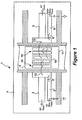
- Figure 1 is a top view of a schematic illustrating a physical layout and bond wire connections of an amplifier section of a broadband amplifier of one embodiment of the invention.
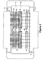
- Figure 2 is a top view of an illustrative LDMOS RF power transistor device embodiment of the invention.
- Figure 3 is a schematic circuit diagram of the exemplary LDMOS RF power transistor device shown in Figure 2.
- Figure 4 is a graph illustrating first and second harmonic frequencies for one embodiment of the invention.
- the present invention generally relates to the field of radio frequency (RF) power transistor devices and, more specifically, to internally matched RF power transistors.
- RF radio frequency
- FIG. 1 illustrates an amplifier section 1 according to one aspect of the invention.
- the amplifier section 1 has a printed circuit board (PCB) 7 and a power transistor pedestal 11.
- the PCB 7 has as RF power input (not shown) for receiving a RF input signal and a RF power output (not shown) for outputting an amplified RF output signal.
- the pedestal 11 has a power transistor 4 attached thereto.
- the power transistor 4 amplifies a phase component signal of the RF input signal to thereby boost the power level from the RF power input to the RF power output as is known in the art.
- the pedestal 11 provides support for the circuit components of the power transistor 4; provides a high electrical conductivity for carrying common currents; and provides high thermal conductivity for cooling.
- the pedestal 11 may be made of copper or a copper alloy with properties optimized for thermal conductivity and electrical conductivity at the operating frequencies of the amplifier section 1.
- the pedestal 11 may be made of any material with similar electrical and thermal properties known to persons of skill.
- the power transistor 4 has field effect transistors having an input (gate), output (drain) and common element (source) terminal formed on a semiconductor die attached to the pedestal 11.
- the transistors are laterally diffused metal oxide semiconductor (LDMOS) transistors, with the source terminal formed on a bottom side of the die and directly attached to the pedestal 11.
- LDMOS laterally diffused metal oxide semiconductor
- the PCB 7 may be a multi-layer module, such as taught in U.S. Pat. No. 6,099,677 to Logothetis et al., incorporated herein by reference.
- Figure 1 illustrates a top view of the physical layout and bond wire connections of the amplifier section 1 of the RF power transistor 4 of the present invention.
- the amplifier section 1 includes an input matching network 2, a gate bias network 3, a power transistor 4, an output matching network 5, and a drain bias network 6. While the illustrated amplifier section 1 is implemented with six amplifier sections, alternate embodiments may be implemented with two or more amplifier sections in accordance with the inventive aspects taught and described herein.
- the input matching network 2 receives RF power in the form of a component input signal from a corresponding output of a splitter, designated as "RF FEED,” to stimulate the gate of a transistor device 10 in the power transistor 4.
- the gate bias network 3 receives a dc bias voltage from an input bias source, designated as "GATE BIAS FEED,” which is used to set the operating point for the transistor device 10.
- the power transistor 4 receives a power RF input component signal from the input matching network 2 and it receives the dc bias from the gate bias network 3.
- the power transistor 4 produces a high power RF output component signal that drives the output matching network 5.
- a combiner, designated as “RF DRIVE” receives the high power RF output component signal from the output matching network 5.
- the source of power, designated as "DRAIN BIAS FEED,” for the high power output component signal is supplied from the drain bias network 6.
- the power transistor 4 has a RF power transistor device 10, in a common source configuration, which is coupled to a pedestal 11.
- the transistor device 10 is a semiconductor having an electrode formed thereon, wherein the electrode has a plurality of interdigitated transistors each having input and output terminals.
- the power transistor 4 has an input 12, an output 13, a gate tuning network 14, and a drain tuning network 15.
- the power transistor input 12 receives RF input power from the input matching network 2 to stimulate the power transistor 4.
- RF output power developed by the power transistor 4 is delivered to the output matching network 5 at the power transistor output 13.
- a bias input 8 transmits a signal from the gate bias network 3 to the input matching network 2.
- a bias output 9 transmits a signal from the output matching network 5 to the drain bias network 6.
- the bond wires used to connect the power transistor 4 to external nodes on the PCB 7, and to interconnect the components of the power transistor 4 located on the pedestal 11, have self-inductance that cannot be neglected at typical frequencies of operation.
- Several impedance transformations and tuning networks effectively couple RF power coming from the RF FEED to the gate of the transistor device 10.
- Similar impedance transformations and tuning networks also effectively couple RF power coming from the drain of the transistor device 10 to the RF DRIVE.
- a gate tuning network 14 compensates for the bond wire inductors and the input capacitance associated with the gate of the transistor device 10 and a drain tuning network 15 compensates for the bond wire inductors and capacitance associated with the drain of the transistor device 10.
- each conduction path may be formed with one or more bond wires. Selecting the number of bond wires applied in parallel, and the length of the bond wires, allows the inductance of the conduction path to be controlled and adjusted to convenient values.
- Figure 2 illustrates the invention using a plurality of bond wires for the input 12 and output 13.
- the broadband RF signal amplifier may have a plurality of power transistor devices 10 attached to a surface of the pedestal 11.
- the signal amplifier may also have an RF input path that has a splitter configured to split a RF input signal into a plurality of component input signals.
- the splitter, the input matching network 2 and the gate bias network 3 may be at least partially implemented in a printed circuit board.
- the signal amplifier may also have an RF output path having a combiner configured to combine component output signals received at the transistor outputs into a RF output signal.
- the combiner, output matching network 5 and drain bias network 6 may be at least partially implemented in a printed circuit board.
- the signal amplifier has RF input and RF output paths 12 and 13 with respective input and output reference ground shelves implemented in a printed circuit board.
- the pedestal 11 and printed circuit board may be arranged such that the input and output reference ground shelves are adjacent the pedestal surface.
- a top view is illustrated of an embodiment of a LDMOS RF power transistor 10 of the present invention.
- the power transistor 4 is positioned between an input lead 2 and an output lead 5 via the input (14 and associated bond wire inductances) and output (15 and associated bond wire inductances).
- the input and output matching networks 2 and 5 are attached to, but electrically isolated from, a conductor 16 by a ceramic substrate 17.
- a pair of transistor devices (semiconductor dies) 10 are attached to a conductor (ground) 16.
- the transistor devices 10 may be attached by an ultrasonic scrubbing and/or thermal heating process.
- Each transistor device 10 has a plurality of interdigitated electrodes, wherein each electrode has an input (gate) terminal and an output (drain) terminal.
- the gate tuning network 14 includes a "T-network.”
- the T-network transforms the impedance "looking" into the transistor input terminal at the fundamental frequency into a low impedance suitable for matching to the transistor device.
- Input matching of the transistor device 10 with the T-network is performed with an input matching capacitor 19.
- the input matching capacitor 19 is located through the conductor 16 near the input matching network 2.
- the input matching capacitor 19 has a first set of terminals 20 coupled to the input matching network 2 by a first set of input bonded wires 21.
- the first set of input bonded wires 21 are bonded at one end to the input matching network 2 and at the other end to the first set of terminals 20 of the input matching capacitor 19.
- the input matching capacitor 19 has a second terminal (not shown) coupled to the conductor (ground) 16.
- a second set of input bonded wires 22 couple the first set of terminals 20 of the input matching capacitor 19 to the respective input terminals of the interdigitated electrodes of the transistor devices 10.
- the second set of input bonded wires 22 is bonded at one end to the to the first set of terminals 20 and at the other end to the respective interdigitated electrode input terminals of the transistor devices 10.
- Input matching of the transistor device 10 is thereby performed by selection of the desired capacitance value of input matching capacitor 19 and the inductance of the first and second sets of input bonded wires 21 and 22.
- An embodiment of the invention with a drain tuning network 15 includes an double-shunt network and a series inductance.
- the series inductance is the result of a first set of output bonded wires 23 connecting the drain of the interdigitated electrode output terminals of the transistor device 10 to the output matching network 5.
- the double-shunt network includes a second set of output bonded wires 24 coupled to a first output matching capacitor 26.
- the first output matching capacitor 26 has a second terminal (not shown) coupled to the conductor (ground) 16.
- the second set of output bonded wires 24 is also coupled to the interdigitated electrode drain terminals of the transistor device 10.
- the double-shunt network also includes a third set of output bonded wires 25 coupled to a second output matching capacitor 27.
- the second output matching capacitor 27 has a second terminal (not shown) coupled to the conductor (ground) 16.
- the third set of output bonded wires 25 is also coupled to the first output matching capacitor 26.
- the values of the first output matching capacitor 26 and the second output matching capacitor 27 are frequency sensitive and are important for the harmonic termination aspect to work.
- the first output matching capacitor 26 may provide a high impedance at a frequency ( f ) and a low impedance at 2 f.
- the second output matching capacitor 27 may provide a low impedance (DC block) at f.
- the power transistor 10 illustrated may be implemented with nominal component values, the skilled practitioner will appreciate that the values of components 19 through 27 may be adjusted in order to achieve tuning for optimal performance from the power transistor 10.
- an embodiment of the present invention has a drain tuning network that includes a double-shunt network.
- the second loop allows 900 MHz devices to be built with enough total inductance to allow for a shunt match at the die plane. This method shortens the drain wires by 1/2 their normal length.
- the double-shunt network of the present invention also provides a second harmonic termination at the die plane. Referring to Figure 4, a graph is shown that illustrates the first and second harmonic frequencies that are produced with the double-shunt network. A first harmonic (900 MHz) is matched by the second set of output bonded wires 24, the third set of output bonded wires 25, and the second output matching capacitor 27 (see Figure 3).
- a second harmonic (2 GHz - may need to adjust small cap value) is matched by the second set of output bonded wires 24 and the first output matching capacitor 26 (see Figure 3).
- a second harmonic termination is added at the die plane (bond loop from die using small cap as a block).
- the double loop tuning allows any dissipated power in the tuning network to be shared between the 2 loops. This effectively doubles the allowable RF dissipation.
Landscapes
- Engineering & Computer Science (AREA)
- Power Engineering (AREA)
- Amplifiers (AREA)
- Microwave Amplifiers (AREA)
Abstract
Description
- The present invention generally relates to the field of radio frequency (RF) power transistor devices and, more specifically, to internally mached RF power transistors.
BACKGROUND - RF power transistor devices are generally known for use as signal amplifiers in wireless communication applications. As demand for wireless communication applications has increased, the operating frequency for wireless networks has also increased. Operating frequencies are now well into the gigahertz range.
- Natural variables in individual transistor elements have made mass production of RF power transistors problematic. Transistor devices naturally vary as to input capacitance, gain and phase shift. Particular transistor devices are preliminarily characterized over a range of expected operating frequencies and voltages. Further devices are then made using like materials in an attempt to make these devices operate within the characterized ranges. Due to the variations in transistors and various other elements over identical operating frequencies and voltages, however, the ability to successfully tune transistor devices on a large scale manufacturing basis is limited.
- RF power transistor devices generally have a plurality of electrodes formed on a silicon die, each electrode having a plurality of interdigitated transistors. The individual transistors of each electrode are connected to respective common input (gate) and output (drain) leads for each electrode. As is known, the die is generally attached by a eutectic die attach process atop a metallic (source) substrate. The substrate is mounted to a metal flange, which serves as both a heat sink and a ground reference. The input (gate) and output (drain) lead frames are attached to the sides of the flange. The lead frames are electrically isolated from the metal (source) substrate and are coupled to the electrode input and output terminals, respectively, on the silicon die by multiple wires (i.e., bonded to the respective terminals and lead frames).
- At high operating frequencies, it is particularly important that the input and output electrode terminals be impedance matched to the desired operating frequency ranges. In lower frequency (i.e.:<1GHz) high power applications, the required inductances of shunt matching elements can cause the wires to be to long and few to handle the operating power. In some cases previous methodologies to solve this have lead to solutions with excessive cross talk between the input and output networks, causing instabilities.
- Examples of RF power transistor devices available in the prior art are illustrated in
U.S. Patent No. 6,177,834 andU.S. Patent No. 6,614,308 , incorporated herein by reference.
SUMMARY - The present invention generally relates to the field of RF power transistor devices and, more specifically, to RF power transistors with an internal output match with a second harmonic termination at the die plane.
- According to one aspect of the invention, there is provided a power transistor, having: a semiconductor having an electrode formed thereon, wherein the electrode comprises at least one transistor comprising input and output terminals, wherein the output terminals of the semiconductor are coupled to an output matching network by a first plurality of output conductors carrying an output inductance; a first output blocking capacitor comprising a first terminal coupled to the output terminals of the semiconductor by a second plurality of output conductors carrying an output inductance and a second terminal coupled to the ground; and a second output blocking capacitor comprising a first terminal coupled to the first terminal of the first output blocking capacitor by a third plurality of output conductors carrying an output inductance and a second terminal coupled to the ground.
- Another aspect of the invention provides a broadband radio frequency (RF) signal amplifier, having: a power transistor attached to a surface of a pedestal having a reference ground, wherein the power transistor comprises at least one transistor device that is electrically connected to an RF input and an RF output, a bias input and a bias output, wherein the at least one transistor device comprises a gate tuning network and a double-shunt drain tuning network; a RF input path electrically connected to the at least one transistor device, an input matching network configured to couple the input signal to the transistor input at an input impedance, and a gate bias network configured to bias the transistor input to an input operating point; and a RF output path electrically connected to the transistor output, an output matching network configured to couple the respective component output signal to the transistor output at an output impedance, and a drain bias network configured to bias the transistor output to an output operating point.
- According to a further aspect of the invention, there is provided a power transistor, having: a semiconductor having an electrode formed thereon, wherein the electrode comprises a plurality of interdigitated transistors each having input and output terminals; a first output blocking capacitor having a first terminal electrically coupled to the output terminals of the interdigitated transistors of the semiconductor and a second terminal electrically coupled to ground; and a second output blocking capacitor having a first terminal electrically coupled to the first terminal of the first output blocking capacitor and a second terminal electrically coupled to ground.
- Still another aspect of the invention provides a method for amplifying signals, the method having the following steps: forming a power transistor on a semiconductor, wherein the power transistor comprises a plurality of interdigitated transistors; shunting an output signal from the plurality of interdigitated transistors; and double-shunting an output signal from the plurality of interdigitated transistors, wherein the shunting and double-shunting generates first and second harmonic terminations at a die plane of the power transistor.
- The objects, features, and advantages of the present invention will be readily apparent to those skilled in the art upon a reading of the description of the preferred embodiments that follows.
- The present invention is better understood by reading the following description of non-limiting embodiments with reference to the attached drawings wherein like parts of each of the several figures are identified by the same referenced characters, and which are briefly described as follows.
- Figure 1 is a top view of a schematic illustrating a physical layout and bond wire connections of an amplifier section of a broadband amplifier of one embodiment of the invention.
- Figure 2 is a top view of an illustrative LDMOS RF power transistor device embodiment of the invention.
- Figure 3 is a schematic circuit diagram of the exemplary LDMOS RF power transistor device shown in Figure 2.
- Figure 4 is a graph illustrating first and second harmonic frequencies for one embodiment of the invention.
- It is to be noted, however, that the appended drawings illustrate only a few aspects of certain embodiments of this invention and are therefore not limiting of its scope, as the invention encompasses equally effective additional or equivalent embodiments.
DETAILED DESCRIPTION - The present invention generally relates to the field of radio frequency (RF) power transistor devices and, more specifically, to internally matched RF power transistors.
- Figure 1 illustrates an amplifier section 1 according to one aspect of the invention. The amplifier section 1 has a printed circuit board (PCB) 7 and a
power transistor pedestal 11. ThePCB 7 has as RF power input (not shown) for receiving a RF input signal and a RF power output (not shown) for outputting an amplified RF output signal. Thepedestal 11 has apower transistor 4 attached thereto. Thepower transistor 4 amplifies a phase component signal of the RF input signal to thereby boost the power level from the RF power input to the RF power output as is known in the art. Thepedestal 11 provides support for the circuit components of thepower transistor 4; provides a high electrical conductivity for carrying common currents; and provides high thermal conductivity for cooling. Thepedestal 11 may be made of copper or a copper alloy with properties optimized for thermal conductivity and electrical conductivity at the operating frequencies of the amplifier section 1. Thepedestal 11 may be made of any material with similar electrical and thermal properties known to persons of skill. - The
power transistor 4 has field effect transistors having an input (gate), output (drain) and common element (source) terminal formed on a semiconductor die attached to thepedestal 11. In one embodiment, the transistors are laterally diffused metal oxide semiconductor (LDMOS) transistors, with the source terminal formed on a bottom side of the die and directly attached to thepedestal 11. The PCB 7 may be a multi-layer module, such as taught inU.S. Pat. No. 6,099,677 to Logothetis et al., incorporated herein by reference. - Figure 1 illustrates a top view of the physical layout and bond wire connections of the amplifier section 1 of the
RF power transistor 4 of the present invention. The amplifier section 1 includes aninput matching network 2, agate bias network 3, apower transistor 4, anoutput matching network 5, and adrain bias network 6. While the illustrated amplifier section 1 is implemented with six amplifier sections, alternate embodiments may be implemented with two or more amplifier sections in accordance with the inventive aspects taught and described herein. - In the amplifier section 1, the
input matching network 2 receives RF power in the form of a component input signal from a corresponding output of a splitter, designated as "RF FEED," to stimulate the gate of atransistor device 10 in thepower transistor 4. Thegate bias network 3 receives a dc bias voltage from an input bias source, designated as "GATE BIAS FEED," which is used to set the operating point for thetransistor device 10. Thepower transistor 4 receives a power RF input component signal from theinput matching network 2 and it receives the dc bias from thegate bias network 3. Thepower transistor 4 produces a high power RF output component signal that drives theoutput matching network 5. A combiner, designated as "RF DRIVE," receives the high power RF output component signal from theoutput matching network 5. The source of power, designated as "DRAIN BIAS FEED," for the high power output component signal is supplied from thedrain bias network 6. - The
power transistor 4 has a RFpower transistor device 10, in a common source configuration, which is coupled to apedestal 11. Thetransistor device 10 is a semiconductor having an electrode formed thereon, wherein the electrode has a plurality of interdigitated transistors each having input and output terminals. Thepower transistor 4 has aninput 12, anoutput 13, agate tuning network 14, and adrain tuning network 15. Thepower transistor input 12 receives RF input power from the input matchingnetwork 2 to stimulate thepower transistor 4. RF output power developed by thepower transistor 4 is delivered to theoutput matching network 5 at thepower transistor output 13. Abias input 8 transmits a signal from thegate bias network 3 to theinput matching network 2. Abias output 9 transmits a signal from the output matchingnetwork 5 to thedrain bias network 6. - The bond wires used to connect the
power transistor 4 to external nodes on thePCB 7, and to interconnect the components of thepower transistor 4 located on thepedestal 11, have self-inductance that cannot be neglected at typical frequencies of operation. Several impedance transformations and tuning networks effectively couple RF power coming from the RF FEED to the gate of thetransistor device 10. Similar impedance transformations and tuning networks also effectively couple RF power coming from the drain of thetransistor device 10 to the RF DRIVE. Agate tuning network 14 compensates for the bond wire inductors and the input capacitance associated with the gate of thetransistor device 10 and adrain tuning network 15 compensates for the bond wire inductors and capacitance associated with the drain of thetransistor device 10. - Although the
input 12 andoutput 13 are depicted as single conductors of minimum length, a skilled practitioner will appreciate that each conduction path may be formed with one or more bond wires. Selecting the number of bond wires applied in parallel, and the length of the bond wires, allows the inductance of the conduction path to be controlled and adjusted to convenient values. Figure 2 illustrates the invention using a plurality of bond wires for theinput 12 andoutput 13. - According to one embodiment of the invention, the broadband RF signal amplifier may have a plurality of
power transistor devices 10 attached to a surface of thepedestal 11. The signal amplifier may also have an RF input path that has a splitter configured to split a RF input signal into a plurality of component input signals. The splitter, theinput matching network 2 and thegate bias network 3 may be at least partially implemented in a printed circuit board. The signal amplifier may also have an RF output path having a combiner configured to combine component output signals received at the transistor outputs into a RF output signal. The combiner,output matching network 5 and drainbias network 6 may be at least partially implemented in a printed circuit board. In further embodiments, the signal amplifier has RF input andRF output paths pedestal 11 and printed circuit board may be arranged such that the input and output reference ground shelves are adjacent the pedestal surface. - Referring to Figure 2, a top view is illustrated of an embodiment of a LDMOS
RF power transistor 10 of the present invention. Thepower transistor 4 is positioned between aninput lead 2 and anoutput lead 5 via the input (14 and associated bond wire inductances) and output (15 and associated bond wire inductances). In one embodiment of the invention, the input andoutput matching networks conductor 16 by aceramic substrate 17. A pair of transistor devices (semiconductor dies) 10 are attached to a conductor (ground) 16. Thetransistor devices 10 may be attached by an ultrasonic scrubbing and/or thermal heating process. Eachtransistor device 10 has a plurality of interdigitated electrodes, wherein each electrode has an input (gate) terminal and an output (drain) terminal. - The
gate tuning network 14 includes a "T-network." In one embodiment of the invention, the T-network transforms the impedance "looking" into the transistor input terminal at the fundamental frequency into a low impedance suitable for matching to the transistor device. Input matching of thetransistor device 10 with the T-network is performed with aninput matching capacitor 19. Theinput matching capacitor 19 is located through theconductor 16 near theinput matching network 2. Theinput matching capacitor 19 has a first set ofterminals 20 coupled to theinput matching network 2 by a first set of input bondedwires 21. The first set of input bondedwires 21 are bonded at one end to theinput matching network 2 and at the other end to the first set ofterminals 20 of theinput matching capacitor 19. Theinput matching capacitor 19 has a second terminal (not shown) coupled to the conductor (ground) 16. A second set of input bondedwires 22 couple the first set ofterminals 20 of theinput matching capacitor 19 to the respective input terminals of the interdigitated electrodes of thetransistor devices 10. In particular, the second set of input bondedwires 22 is bonded at one end to the to the first set ofterminals 20 and at the other end to the respective interdigitated electrode input terminals of thetransistor devices 10. Input matching of thetransistor device 10 is thereby performed by selection of the desired capacitance value ofinput matching capacitor 19 and the inductance of the first and second sets of input bondedwires - An embodiment of the invention with a
drain tuning network 15 includes an double-shunt network and a series inductance. The series inductance is the result of a first set of output bondedwires 23 connecting the drain of the interdigitated electrode output terminals of thetransistor device 10 to theoutput matching network 5. The double-shunt network includes a second set of output bondedwires 24 coupled to a firstoutput matching capacitor 26. The firstoutput matching capacitor 26 has a second terminal (not shown) coupled to the conductor (ground) 16. The second set of output bondedwires 24 is also coupled to the interdigitated electrode drain terminals of thetransistor device 10. The double-shunt network also includes a third set of output bondedwires 25 coupled to a secondoutput matching capacitor 27. The secondoutput matching capacitor 27 has a second terminal (not shown) coupled to the conductor (ground) 16. The third set of output bondedwires 25 is also coupled to the firstoutput matching capacitor 26. In some embodiments of the invention, the values of the firstoutput matching capacitor 26 and the secondoutput matching capacitor 27 are frequency sensitive and are important for the harmonic termination aspect to work. The firstoutput matching capacitor 26 may provide a high impedance at a frequency (f) and a low impedance at 2f. The secondoutput matching capacitor 27 may provide a low impedance (DC block) at f. - Although the
power transistor 10 illustrated may be implemented with nominal component values, the skilled practitioner will appreciate that the values ofcomponents 19 through 27 may be adjusted in order to achieve tuning for optimal performance from thepower transistor 10. - As noted above, an embodiment of the present invention has a drain tuning network that includes a double-shunt network. The second loop allows 900 MHz devices to be built with enough total inductance to allow for a shunt match at the die plane. This method shortens the drain wires by 1/2 their normal length. The double-shunt network of the present invention also provides a second harmonic termination at the die plane. Referring to Figure 4, a graph is shown that illustrates the first and second harmonic frequencies that are produced with the double-shunt network. A first harmonic (900 MHz) is matched by the second set of output bonded
wires 24, the third set of output bondedwires 25, and the second output matching capacitor 27 (see Figure 3). A second harmonic (2 GHz - may need to adjust small cap value) is matched by the second set of output bondedwires 24 and the first output matching capacitor 26 (see Figure 3). Thus, according to a further embodiment of the invention, a second harmonic termination is added at the die plane (bond loop from die using small cap as a block). At operating frequencies the double loop tuning allows any dissipated power in the tuning network to be shared between the 2 loops. This effectively doubles the allowable RF dissipation. - Therefore, the present invention is well adapted to carry out the objects and attain the ends and advantages mentioned as well as those that are inherent therein. While numerous changes may be made by those skilled in the art, such changes are encompassed within the spirit of this invention as defined by the appended claims.
Claims (24)
- An output match transistor, comprising:a semiconductor having an electrode formed thereon, wherein the electrode comprises at least one transistor comprising input and output terminals, wherein the output terminals of the semiconductor are coupled to an output matching network by a first plurality of output conductors carrying an output inductance;a first output blocking capacitor comprising a first terminal coupled to the output terminals of the semiconductor by a second plurality of output conductors carrying an output inductance and a second terminal coupled to the ground; anda second output blocking capacitor comprising a first terminal coupled to the first terminal of the first ouput blocking capacitor by a third plurality of output conductors carrying an output inductance and a second terminal coupled to the ground.
- An output match transistor as claimed in claim 1, wherein the semiconductor is a LDMOS transistor.
- An output match transistor as claimed in claim 1, wherein the first output blocking capacitor is positioned between the electrode and the output matching network.
- An output match transistor as claimed in claim 1, wherein the second output blocking capacitor is positioned between the electrode and the output matching network.
- An output match transistor as claimed in claim 1, further comprising an input matching capacitor comprising a first terminal coupled to an input matching network by a first plurality of input conductors carrying an input inductance and a second terminal coupled to a ground, wherein the first terminal is also coupled to the input terminals of the semiconductor by a second plurality of input conductors carrying an input inductance.
- An output match transistor as claimed in claim 5, wherein the input matching capacitor is positioned between the input matching network and the electrode.
- A broadband radio frequency (RF) signal amplifier, comprising:a power transistor attached to a surface of a pedestal comprising a reference ground, wherein the power transistor comprises at least one transistor device that is electrically connected to an RF input and an RF output, a bias input and a bias output, wherein the at least one transistor device comprises a gate tuning network and a double-shunt drain tuning network;a RF input path electrically connected to the at least one transistor device, an input matching network configured to couple the input signal to the transistor input at an input inductance, and a gate bias network configured to bias the transistor input to an input operating point; anda RF output path electrically connected to the transistor output, an output matching network configured to couple the respective component output signal to the transistor output at an output inductance, and a drain bias network configured to bias the transistor output to an output operating point.
- A broadband RF signal amplifier as claimed in claim 7, wherein the double-shunt drain tuning network comprises:a first output blocking capacitor comprising a first terminal coupled to the output terminals of the at least one transistor device by a first plurality of output conductors carrying an output inductance and a second terminal coupled to the reference ground; anda second output blocking capacitor comprising a first terminal coupled to the first terminal of the first ouput blocking capacitor by a second plurality of output conductors carrying an output inductance and a second terminal coupled to the reference ground.
- A broadband RF signal amplifier as claimed in claim 7, wherein a plurality of power transistors are attached to a surface of a pedestal.
- A broadband RF signal amplifier as claimed in claim 7, wherein the RF input path comprises a splitter configured to split a RF input signal into a plurality of component input signals and wherein the splitter, input matching network and gate bias network are at least partially implemented in a printed circuit board.
- A broadband RF signal amplifier as claimed in claim 7, wherein the RF output path comprises a combiner configured to combine component output signals received at the transistor outputs into a RF output signal, and wherein the combiner, output matching networks and drain bias networks at least partially are implemented in a printed circuit board.
- A broadband RF signal amplifier as claimed in claim 7, wherein the RF input and RF output paths comprise respective input and output reference ground shelves implemented in a printed circuit board, and the pedestal and printed circuit board are arranged such that the input and output reference ground shelves are adjacent the pedestal surface.
- A power transistor, comprising:a semiconductor having an electrode formed thereon, wherein the electrode comprises at least one transistor comprising input and output terminals;a first output blocking capacitor comprising a first terminal electrically coupled to the output terminals of the electrode of the semiconductor and a second terminal electrically coupled to ground; anda second output blocking capacitor comprising a first terminal electrically coupled to the first terminal of the first ouput blocking capacitor and a second terminal electrically coupled to ground.
- A power transistor as claimed in claim 13, wherein the first output blocking capacitor is positioned between the electrode and the second output blocking capacitor.
- A power transistor as claimed in claim 13, wherein the first terminal of the first output blocking capacitor is electrically coupled to the output terminals of the electrode by a plurality of conductors carrying an output inductance.
- A power transistor as claimed in claim 13, wherein the first terminal of the second output blocking capacitor is electrically coupled to the first terminal of the first output blocking capacitor by a plurality of conductors carrying an output inductance.
- A method for amplifying signals, the method comprising:forming a power transistor on a semiconductor, wherein the power transistor comprises a plurality of interdigitated transistors;shunting an output signal from the plurality of interdigitated transistors; anddouble-shunting an output signal from the plurality of interdigitated transistors, wherein the shunting and double-shunting generates first and second harmonic terminations at a die plane of the power transistor.
- A method for amplifying signals as claimed in claim 17, wherein the shunting comprises eletrically connecting a first output blocking capacitor to at least one of the plurality of interdigitated transistors.
- A method for amplifying signals as claimed in claim 18, wherein the double-shunting comprises electrically coupling a second output blocking capacitor to the first ouput blocking capacitor.
- A method for amplifying signals as claimed in claim 17, further comprising matching an input signal from an input matching network with a matching capacitor electrically connected to the input matching network.
- A power transistor, comprising:a semiconductor having an electrode formed thereon, wherein the electrode comprises at least one transistor comprising input and output terminals;a first means for blocking output power electrically coupled to the output terminals of the electrode of the semiconductor and electrically coupled to ground; anda second means for blocking output power electrically coupled to the first means for blocking output power and electrically coupled to ground.
- A power transistor as claimed in claim 21, wherein the first means for blocking output power is positioned between the electrode and the second means for blocking output power.
- A power transistor as claimed in claim 21, wherein the first and second means for blocking output power generate first and second harmonic terminations at a die plane of the power transistor.
- A power transistor as claimed in claim 21, further comprising a means for matching input power electrically connected to an input matching network.
Applications Claiming Priority (1)
| Application Number | Priority Date | Filing Date | Title |
|---|---|---|---|
| US11/189,615 US7372334B2 (en) | 2005-07-26 | 2005-07-26 | Output match transistor |
Publications (3)
| Publication Number | Publication Date |
|---|---|
| EP1750298A2 true EP1750298A2 (en) | 2007-02-07 |
| EP1750298A3 EP1750298A3 (en) | 2007-05-09 |
| EP1750298B1 EP1750298B1 (en) | 2012-01-18 |
Family
ID=37414387
Family Applications (1)
| Application Number | Title | Priority Date | Filing Date |
|---|---|---|---|
| EP06015435A Active EP1750298B1 (en) | 2005-07-26 | 2006-07-25 | RF power transistor with impedance matched output electrode |
Country Status (4)
| Country | Link |
|---|---|
| US (1) | US7372334B2 (en) |
| EP (1) | EP1750298B1 (en) |
| KR (1) | KR100797086B1 (en) |
| CN (1) | CN1976023B (en) |
Cited By (7)
| Publication number | Priority date | Publication date | Assignee | Title |
|---|---|---|---|---|
| EP2162914A2 (en) * | 2007-06-22 | 2010-03-17 | Cree, Inc. | Rf power transistor packages with internal harmonic frequency reduction and methods of forming rf power transistor packages with internal harmonic frequency reduction |
| EP2388815A1 (en) * | 2010-05-10 | 2011-11-23 | Nxp B.V. | A transistor package |
| EP2802075A1 (en) * | 2013-05-07 | 2014-11-12 | Nxp B.V. | Dual-band semiconductor RF amplifier device |
| EP3113360A4 (en) * | 2014-03-21 | 2017-03-08 | Huawei Technologies Co., Ltd. | Power amplification circuit and transmitter |
| EP3154193A1 (en) * | 2015-10-08 | 2017-04-12 | MACOM Technology Solutions Holdings, Inc. | Tuned semiconductor amplifier |
| US11158575B2 (en) | 2018-06-05 | 2021-10-26 | Macom Technology Solutions Holdings, Inc. | Parasitic capacitance reduction in GaN-on-silicon devices |
| US11437972B2 (en) | 2016-04-15 | 2022-09-06 | Macom Technology Solutions Holdings, Inc. | Ultra-broad bandwidth matching technique |
Families Citing this family (47)
| Publication number | Priority date | Publication date | Assignee | Title |
|---|---|---|---|---|
| GB2411062B (en) * | 2004-02-11 | 2007-11-28 | Nujira Ltd | Resonance suppression for power amplifier output network |
| US7961470B2 (en) * | 2006-07-19 | 2011-06-14 | Infineon Technologies Ag | Power amplifier |
| US20080231373A1 (en) * | 2007-03-20 | 2008-09-25 | Hafizur Rahman | Output Circuit |
| US9741673B2 (en) * | 2007-06-22 | 2017-08-22 | Cree, Inc. | RF transistor packages with high frequency stabilization features and methods of forming RF transistor packages with high frequency stabilization features |
| EP2164170A1 (en) * | 2008-09-15 | 2010-03-17 | Forschungsverbund Berlin E.V. | Self-adjusting gate bias network for field effect transistors |
| JP5631607B2 (en) * | 2009-08-21 | 2014-11-26 | 株式会社東芝 | High frequency circuit having multi-chip module structure |
| CN101726698B (en) * | 2009-12-25 | 2012-05-09 | 北京铁路信号有限公司 | Method and device for pairing triodes |
| US8659359B2 (en) | 2010-04-22 | 2014-02-25 | Freescale Semiconductor, Inc. | RF power transistor circuit |
| US7990223B1 (en) * | 2010-05-31 | 2011-08-02 | Kabushiki Kaisha Toshiba | High frequency module and operating method of the same |
| US20110309872A1 (en) | 2010-06-17 | 2011-12-22 | Cynthia Blair | Voltage Spike Protection for Power DMOS Devices |
| EP2458730B8 (en) | 2010-11-29 | 2015-08-05 | Nxp B.V. | Radiofrequency amplifier |
| EP2463905B1 (en) * | 2010-12-10 | 2014-10-01 | Nxp B.V. | Packaged RF transistor with special supply voltage leads |
| US8299856B2 (en) * | 2010-12-20 | 2012-10-30 | Infineon Technologies Ag | Power transistor output match network with high Q RF path and low Q low frequency path |
| US8963645B1 (en) | 2011-04-08 | 2015-02-24 | Lockheed Martin Corporation | Integrated-circuit amplifier with low temperature rise |
| US8466747B1 (en) * | 2011-04-08 | 2013-06-18 | Lockheed Martin Corporation | Integrated-circuit amplifier with low temperature rise |
| US8983406B2 (en) * | 2011-07-08 | 2015-03-17 | Skyworks Solutions, Inc. | Signal path termination |
| US9679869B2 (en) | 2011-09-02 | 2017-06-13 | Skyworks Solutions, Inc. | Transmission line for high performance radio frequency applications |
| WO2013067031A2 (en) | 2011-11-04 | 2013-05-10 | Skyworks Solutions, Inc. | Apparatus and methods for power amplifiers |
| US9876478B2 (en) | 2011-11-04 | 2018-01-23 | Skyworks Solutions, Inc. | Apparatus and methods for wide local area network power amplifiers |
| CN103988424B (en) | 2011-11-11 | 2017-03-08 | 天工方案公司 | Flip Chip Linear Power Amplifier with High Power Added Efficiency |
| KR101584042B1 (en) | 2012-06-14 | 2016-01-08 | 스카이워크스 솔루션즈, 인코포레이티드 | Power amplifier modules including related systems, devices, and methods |
| CN104396141B (en) * | 2012-06-29 | 2018-04-10 | 克里公司 | The radio frequency crystals tube device of encapsulation |
| US8964427B2 (en) | 2012-06-29 | 2015-02-24 | Rockwell Automation Technologies, Inc. | Adaptive online filter for DC offset elimination |
| US9281283B2 (en) | 2012-09-12 | 2016-03-08 | Freescale Semiconductor, Inc. | Semiconductor devices with impedance matching-circuits |
| US9373577B2 (en) * | 2013-05-21 | 2016-06-21 | Infineon Technologies Ag | Hybrid semiconductor package |
| US9419568B2 (en) | 2013-06-03 | 2016-08-16 | Skyworks Solutions, Inc. | Circuits and methods related to power amplifier efficiency based on multi-harmonic approximation |
| EP2830089B1 (en) * | 2013-07-25 | 2017-07-12 | Ampleon Netherlands B.V. | RF power device |
| EP2879174B1 (en) * | 2013-11-29 | 2021-09-08 | Ampleon Netherlands B.V. | Packaged RF power transistor device having next to each other ground leads and a video lead for connecting decoupling capacitors, RF power amplifier |
| US9438184B2 (en) | 2014-06-27 | 2016-09-06 | Freescale Semiconductor, Inc. | Integrated passive device assemblies for RF amplifiers, and methods of manufacture thereof |
| CN104218029A (en) * | 2014-08-27 | 2014-12-17 | 昆山华太电子技术有限公司 | Internal matching structure for power transistor |
| US10432152B2 (en) | 2015-05-22 | 2019-10-01 | Nxp Usa, Inc. | RF amplifier output circuit device with integrated current path, and methods of manufacture thereof |
| CN106470014B (en) * | 2015-08-17 | 2019-10-18 | 恩智浦美国有限公司 | The output impedance matching networks of circuit are prevented with harmonic wave |
| US9692363B2 (en) | 2015-10-21 | 2017-06-27 | Nxp Usa, Inc. | RF power transistors with video bandwidth circuits, and methods of manufacture thereof |
| US9571044B1 (en) | 2015-10-21 | 2017-02-14 | Nxp Usa, Inc. | RF power transistors with impedance matching circuits, and methods of manufacture thereof |
| CN109417364A (en) * | 2016-07-01 | 2019-03-01 | 三菱电机株式会社 | Amplifier |
| NL2017349B1 (en) * | 2016-08-23 | 2018-03-06 | Ampleon Netherlands Bv | Packaged RF power amplifier having a high power density |
| US9979361B1 (en) * | 2016-12-27 | 2018-05-22 | Nxp Usa, Inc. | Input circuits for RF amplifier devices, and methods of manufacture thereof |
| CN106959389B (en) * | 2017-03-17 | 2019-04-05 | 成都海威华芯科技有限公司 | A kind of frequency-division section load balance factor test method |
| JP2019041311A (en) * | 2017-08-28 | 2019-03-14 | 株式会社村田製作所 | Power amplifier circuit |
| NL2020069B1 (en) * | 2017-12-12 | 2019-06-21 | Ampleon Netherlands Bv | Packaged RF power amplifier |
| US10742178B2 (en) * | 2018-05-18 | 2020-08-11 | Nxp Usa, Inc. | Broadband power transistor devices and amplifiers and methods of manufacture thereof |
| IT201800010793A1 (en) * | 2018-12-04 | 2020-06-04 | St Microelectronics Srl | Corresponding detection circuit, device and method |
| US11082016B2 (en) | 2019-05-15 | 2021-08-03 | Nxp Usa, Inc. | Amplifier devices with reflection absorption |
| US11012035B2 (en) | 2019-05-15 | 2021-05-18 | Nxp Usa, Inc. | Amplifier devices with input transient termination |
| CN110856339B (en) * | 2019-11-22 | 2021-02-09 | 普联技术有限公司 | Planar circuit for signal cross transmission |
| US12159845B2 (en) * | 2022-02-16 | 2024-12-03 | Nxp Usa, Inc. | Transistor with integrated passive components |
| KR102830332B1 (en) * | 2022-12-09 | 2025-07-08 | 한국전자통신연구원 | Semiconductor package |
Citations (3)
| Publication number | Priority date | Publication date | Assignee | Title |
|---|---|---|---|---|
| US6099677A (en) | 1998-02-13 | 2000-08-08 | Merrimac Industries, Inc. | Method of making microwave, multifunction modules using fluoropolymer composite substrates |
| US6177834B1 (en) | 1998-12-02 | 2001-01-23 | Ericsson, Inc. | Output matched LDMOS power transistor device |
| US6614308B2 (en) | 2001-10-22 | 2003-09-02 | Infineon Technologies Ag | Multi-stage, high frequency, high power signal amplifier |
Family Cites Families (10)
| Publication number | Priority date | Publication date | Assignee | Title |
|---|---|---|---|---|
| US4580114A (en) | 1984-09-14 | 1986-04-01 | Rca Corporation | Active element microwave power coupler |
| JPH0653761A (en) * | 1992-08-03 | 1994-02-25 | Fujitsu Ltd | High frequency amplifier |
| US5535438A (en) | 1994-05-10 | 1996-07-09 | Panasonic Technologies, Inc. | Phase linear class E amplifier for a satellite communication terminal which communicates with a low earth orbiting satellite |
| JP2003521127A (en) | 2000-01-28 | 2003-07-08 | エリクソン インコーポレイテッド | Multiple earth signal path LDMOS power package |
| US6466094B2 (en) | 2001-01-10 | 2002-10-15 | Ericsson Inc. | Gain and bandwidth enhancement for RF power amplifier package |
| EP1490907A1 (en) * | 2002-03-21 | 2004-12-29 | Koninklijke Philips Electronics N.V. | Power amplifier device |
| US6822321B2 (en) | 2002-09-30 | 2004-11-23 | Cree Microwave, Inc. | Packaged RF power transistor having RF bypassing/output matching network |
| US6734728B1 (en) | 2002-12-19 | 2004-05-11 | Infineon Technologies North America Corp. | RF power transistor with internal bias feed |
| US7158386B2 (en) * | 2003-05-08 | 2007-01-02 | Powerwave Technologies, Inc. | Balanced radio frequency power amplifier with temperature compensation |
| KR100544958B1 (en) * | 2003-12-10 | 2006-01-24 | 한국전자통신연구원 | Adjustable Band Low Noise Amplifier |
-
2005
- 2005-07-26 US US11/189,615 patent/US7372334B2/en not_active Expired - Lifetime
-
2006
- 2006-07-25 EP EP06015435A patent/EP1750298B1/en active Active
- 2006-07-25 CN CN2006101363991A patent/CN1976023B/en active Active
- 2006-07-26 KR KR1020060070284A patent/KR100797086B1/en active Active
Patent Citations (3)
| Publication number | Priority date | Publication date | Assignee | Title |
|---|---|---|---|---|
| US6099677A (en) | 1998-02-13 | 2000-08-08 | Merrimac Industries, Inc. | Method of making microwave, multifunction modules using fluoropolymer composite substrates |
| US6177834B1 (en) | 1998-12-02 | 2001-01-23 | Ericsson, Inc. | Output matched LDMOS power transistor device |
| US6614308B2 (en) | 2001-10-22 | 2003-09-02 | Infineon Technologies Ag | Multi-stage, high frequency, high power signal amplifier |
Cited By (16)
| Publication number | Priority date | Publication date | Assignee | Title |
|---|---|---|---|---|
| EP2162914A2 (en) * | 2007-06-22 | 2010-03-17 | Cree, Inc. | Rf power transistor packages with internal harmonic frequency reduction and methods of forming rf power transistor packages with internal harmonic frequency reduction |
| EP2388815A1 (en) * | 2010-05-10 | 2011-11-23 | Nxp B.V. | A transistor package |
| EP2802075A1 (en) * | 2013-05-07 | 2014-11-12 | Nxp B.V. | Dual-band semiconductor RF amplifier device |
| US9450545B2 (en) | 2013-05-07 | 2016-09-20 | Ampleon Netherlands B.V. | Dual-band semiconductor RF amplifier device |
| US9866181B2 (en) | 2014-03-21 | 2018-01-09 | Huawei Technologies Co., Ltd. | Power amplification circuit and transmitter |
| EP3113360A4 (en) * | 2014-03-21 | 2017-03-08 | Huawei Technologies Co., Ltd. | Power amplification circuit and transmitter |
| EP3154193A1 (en) * | 2015-10-08 | 2017-04-12 | MACOM Technology Solutions Holdings, Inc. | Tuned semiconductor amplifier |
| US9722032B2 (en) | 2015-10-08 | 2017-08-01 | Macom Technology Solutions Holdings, Inc. | Tuned semiconductor amplifier |
| US9806159B2 (en) | 2015-10-08 | 2017-10-31 | Macom Technology Solutions Holdings, Inc. | Tuned semiconductor amplifier |
| US10204992B2 (en) | 2015-10-08 | 2019-02-12 | Macom Technology Solutions Holdings, Inc. | Tuned semiconductor amplifier |
| EP3742607A1 (en) * | 2015-10-08 | 2020-11-25 | MACOM Technology Solutions Holdings, Inc. | Tuned semiconductor amplifier |
| US11437972B2 (en) | 2016-04-15 | 2022-09-06 | Macom Technology Solutions Holdings, Inc. | Ultra-broad bandwidth matching technique |
| US11689175B2 (en) | 2016-04-15 | 2023-06-27 | Macom Technology Solutions Holdings, Inc. | Ultra-broad bandwidth matching technique |
| US11158575B2 (en) | 2018-06-05 | 2021-10-26 | Macom Technology Solutions Holdings, Inc. | Parasitic capacitance reduction in GaN-on-silicon devices |
| US11929364B2 (en) | 2018-06-05 | 2024-03-12 | Macom Technology Solutions Holdings, Inc. | Parasitic capacitance reduction in GaN devices |
| US12266523B2 (en) | 2018-06-05 | 2025-04-01 | Macom Technology Solutions Holdings, Inc. | Parasitic capacitance reduction in GaN-on-silicon devices |
Also Published As
| Publication number | Publication date |
|---|---|
| US20070024374A1 (en) | 2007-02-01 |
| KR20070014076A (en) | 2007-01-31 |
| EP1750298B1 (en) | 2012-01-18 |
| KR100797086B1 (en) | 2008-01-22 |
| CN1976023A (en) | 2007-06-06 |
| EP1750298A3 (en) | 2007-05-09 |
| CN1976023B (en) | 2011-03-09 |
| US7372334B2 (en) | 2008-05-13 |
Similar Documents
| Publication | Publication Date | Title |
|---|---|---|
| EP1750298B1 (en) | RF power transistor with impedance matched output electrode | |
| US6177834B1 (en) | Output matched LDMOS power transistor device | |
| CN100459121C (en) | Internally Biased RF Power Transistors | |
| US6614308B2 (en) | Multi-stage, high frequency, high power signal amplifier | |
| US6046641A (en) | Parallel HV MOSFET high power stable amplifier | |
| CN110504922A (en) | Broadband power transistor unit and amplifier and its manufacturing method | |
| CN110504923A (en) | Transistor unit and amplifier with harmonic termination circuit and its manufacturing method | |
| TW201842729A (en) | Improved efficiency of symmetric DOHERTY power amplifiers | |
| WO2002056462A2 (en) | Gain and bandwidth enhancement for rf power amplifier package | |
| CN118156230A (en) | Power amplifier module | |
| US7432778B2 (en) | Arrangement and method impedance matching | |
| JP2010021961A (en) | amplifier | |
| JP4990903B2 (en) | Apparatus comprising an element having an electrode coupled to a connection | |
| US20250105804A1 (en) | Amplify device and semiconductor device | |
| CN119382644A (en) | Radio frequency power amplifier device and manufacturing method thereof | |
| JP2006332136A (en) | High frequency semiconductor device | |
| JP2005051062A (en) | Semiconductor device | |
| HK1064208B (en) | Arrangement and method for impedance matching | |
| JPH0851327A (en) | High frequency amplifier |
Legal Events
| Date | Code | Title | Description |
|---|---|---|---|
| PUAI | Public reference made under article 153(3) epc to a published international application that has entered the european phase |
Free format text: ORIGINAL CODE: 0009012 |
|
| AK | Designated contracting states |
Kind code of ref document: A2 Designated state(s): AT BE BG CH CY CZ DE DK EE ES FI FR GB GR HU IE IS IT LI LT LU LV MC NL PL PT RO SE SI SK TR |
|
| AX | Request for extension of the european patent |
Extension state: AL BA HR MK YU |
|
| RIC1 | Information provided on ipc code assigned before grant |
Ipc: H01L 23/66 20060101ALI20070116BHEP Ipc: H01L 23/50 20060101ALI20070116BHEP Ipc: H01L 21/66 20060101AFI20061123BHEP Ipc: H03F 1/56 20060101ALI20070116BHEP |
|
| PUAL | Search report despatched |
Free format text: ORIGINAL CODE: 0009013 |
|
| AK | Designated contracting states |
Kind code of ref document: A3 Designated state(s): AT BE BG CH CY CZ DE DK EE ES FI FR GB GR HU IE IS IT LI LT LU LV MC NL PL PT RO SE SI SK TR |
|
| AX | Request for extension of the european patent |
Extension state: AL BA HR MK YU |
|
| 17P | Request for examination filed |
Effective date: 20070530 |
|
| 17Q | First examination report despatched |
Effective date: 20070702 |
|
| AKX | Designation fees paid |
Designated state(s): DE |
|
| RAP1 | Party data changed (applicant data changed or rights of an application transferred) |
Owner name: INFINEON TECHNOLOGIES AG |
|
| GRAP | Despatch of communication of intention to grant a patent |
Free format text: ORIGINAL CODE: EPIDOSNIGR1 |
|
| GRAS | Grant fee paid |
Free format text: ORIGINAL CODE: EPIDOSNIGR3 |
|
| GRAA | (expected) grant |
Free format text: ORIGINAL CODE: 0009210 |
|
| AK | Designated contracting states |
Kind code of ref document: B1 Designated state(s): DE |
|
| REG | Reference to a national code |
Ref country code: DE Ref legal event code: R096 Ref document number: 602006027119 Country of ref document: DE Effective date: 20120315 |
|
| PLBE | No opposition filed within time limit |
Free format text: ORIGINAL CODE: 0009261 |
|
| STAA | Information on the status of an ep patent application or granted ep patent |
Free format text: STATUS: NO OPPOSITION FILED WITHIN TIME LIMIT |
|
| 26N | No opposition filed |
Effective date: 20121019 |
|
| REG | Reference to a national code |
Ref country code: DE Ref legal event code: R097 Ref document number: 602006027119 Country of ref document: DE Effective date: 20121019 |
|
| REG | Reference to a national code |
Ref country code: DE Ref legal event code: R081 Ref document number: 602006027119 Country of ref document: DE Owner name: WOLFSPEED, INC., DURHAM, US Free format text: FORMER OWNER: INFINEON TECHNOLOGIES AG, 85579 NEUBIBERG, DE Ref country code: DE Ref legal event code: R081 Ref document number: 602006027119 Country of ref document: DE Owner name: CREE, INC., DURHAM, US Free format text: FORMER OWNER: INFINEON TECHNOLOGIES AG, 85579 NEUBIBERG, DE |
|
| REG | Reference to a national code |
Ref country code: DE Ref legal event code: R081 Ref document number: 602006027119 Country of ref document: DE Owner name: WOLFSPEED, INC., DURHAM, US Free format text: FORMER OWNER: CREE, INC., DURHAM, NC, US Ref country code: DE Ref legal event code: R081 Ref document number: 602006027119 Country of ref document: DE Owner name: MACOM TECHNOLOGY SOLUTIONS HOLDINGS, INC., LOW, US Free format text: FORMER OWNER: CREE, INC., DURHAM, NC, US |
|
| P01 | Opt-out of the competence of the unified patent court (upc) registered |
Effective date: 20230609 |
|
| PGFP | Annual fee paid to national office [announced via postgrant information from national office to epo] |
Ref country code: DE Payment date: 20250728 Year of fee payment: 20 |
|
| REG | Reference to a national code |
Ref country code: DE Ref legal event code: R079 Ref document number: 602006027119 Country of ref document: DE Free format text: PREVIOUS MAIN CLASS: H01L0021660000 Ipc: H10P0074000000 |
|
| REG | Reference to a national code |
Ref country code: DE Ref legal event code: R081 Ref document number: 602006027119 Country of ref document: DE Owner name: MACOM TECHNOLOGY SOLUTIONS HOLDINGS, INC., LOW, US Free format text: FORMER OWNER: WOLFSPEED, INC., DURHAM, NC, US |